UBS Axcera LL50ATC 50-Watt, 1.6 GHz DVB-H Transmitter User Manual LL50ATC operators manual
UBS-Axcera 50-Watt, 1.6 GHz DVB-H Transmitter LL50ATC operators manual
Contents
- 1. Pro Televsion Modulator Manual
- 2. LL50ATC User Manual
LL50ATC User Manual

INSTRUCTION MANUAL
(Preliminary)
INNOVATOR LX SERIES
1.67 GHz 50W DVB-H TRANSMITTER
AXCERA, LLC
103 FREEDOM DRIVE P.O. BOX 525 LAWRENCE, PA 15055-0525 USA
(724) 873-8100 • FAX (724) 873-8105
www.axcera.com • info@axcera.com

1.67 GHz 50 Watt Single Output Transmitter Chapter 1, Introduction
LL50ATC, Rev. 0 1-1
Chapter 1
Introduction
1.1 Manual Overview
This manual provides descriptions of the
transmitter and associated equipment
along with the set up and operating
procedures. It is important that you
read all of the instructions, especially
the safety information in this chapter,
before you begin operating the unit.
This instruction manual is divided into
five chapters and supporting appendices.
Chapter 1, Introduction, contains
information on the assembly numbering
system used in the manual, safety,
contact information, return procedures,
and warranties. Chapter 2, System
Description, includes overview of entire
transmitter system. Chapter 3, Circuit
Descriptions, contains circuit level
descriptions for boards and board level
components in the transmitter. Chapter
4, Transmitter Tuning Procedure,
provides information on adjusting the
system for optimal operation. Appendix
A contains system specifications.
Appendix B contains Site Drawings.
Appendix C contains a list of Modules
and Site ID. Appendix D Site
Acceptance Document.
1.2 Assembly Designators
Axcera has assigned assembly numbers,
Ax designations such as A1, where
x=1,2,3…etc, to all assemblies, modules,
and boards in the system.
These designations are referenced in the
text of this manual and shown on the
drawings provided in the appendices.
The cables that connect between the
boards within a tray or assembly and
that connect between the trays, racks
and cabinets are labeled using Brady
markers.
Figure 1-1 is an example of a Brady
marked cable. There may be as few as
two or as many as four Markers on any
one cable. These Brady markers are
read starting furthest from the
connector. If there are four Brady
Markers, this marker is the transmitter
number such as transmitter 1 or
Transmitter 2. The next or the furthest
Brady Marker is the rack or cabinet
number on an interconnect cable or the
board number within a tray. The next
number on an interconnect cable is the
Tray location or number. The Brady
marker closest to the connector is the
Jack or Connector number on an
interconnect cable or the jack or
connector number on the board within a
tray.
Figure 1-1 Brady Marker Identification Drawing

1.67 GHz 50 Watt Single Output Transmitter Chapter 1, Introduction
LL50ATC, Rev. 0 1-2
1.3 Safety
The 1.67 GHz transmitter systems
manufactured by Axcera are designed to
be easy to use and repair while providing
protection from electrical and mechanical
hazards. Please review the following
warnings and familiarize yourself with the
operation and servicing procedures
before working on the transmitter
system.
Read All safety Instructions – All of
the safety instructions should be read
and understood before operating this
equipment.
Retain Manuals – The manuals for the
transmitter should be retained at the
transmitter site for future reference.
Axcera provides two sets of manuals for
this purpose; one set can be left at the
office while one set can be kept at the
site.
Heed all Notes, Warnings, and
Cautions – All of the notes, warnings,
and cautions listed in this safety section
and throughout the manual must be
followed.
Follow Operating Instructions – All of
the operating and use instructions for the
transmitter should be followed.
Cleaning – Unplug or otherwise
disconnect all power from the equipment
before cleaning. Do not use liquid or
aerosol cleaners. Use a damp cloth for
cleaning.
Ventilation – Openings in the cabinet
and module front panels are provided for
ventilation. To ensure the reliable
operation of the driver/transmitter, and
to protect the unit from overheating,
these openings must not be blocked.
Servicing – Do not attempt to service
this product yourself until becoming
familiar with the equipment. If in doubt,
refer all servicing questions to qualified
Axcera service personnel.
Replacement Parts – When
replacement parts are used, be sure that
the parts have the same functional and
performance characteristics as the
original part. Unauthorized substitutions
may result in fire, electric shock, or other
hazards. Please contact the Axcera
Technical Service Department if you have
any questions regarding service or
replacement parts.
1.4 Contact Information
The Axcera Field Service Department can
be contacted by phone at (724) 873-
8100 or by fax at (724) 873-8105.
Before calling Axcera, please be prepared
to supply the Axcera technician with
answers to the following questions. This
will save time and help ensure the most
direct resolution to the problem.
1. What are the Customers’ Name and
call letters?
2. What are the model number and
type of transmitter?
3. How long has the transmitter been
on the air? (Approximately when was
the transmitter installed.)
4. What are the symptoms being
exhibited by the transmitter? Include
the current control/power supply
LCD readings and the status of LEDs
on the front panels of the modules.
If possible, include the control/power
supply LCD readings before the
problem occurred.
1.5 Material Return Procedure
To insure the efficient handling of
equipment or components that have been
returned for repair, Axcera requests that
each returned item be accompanied by a
Material Return Authorization Number
(MRA#).
The MRA# can be obtained from any
Axcera Field Service Engineer by
contacting the Axcera Field Service
Department at (724) 873-8100 or by fax
at (724) 873-8105. This procedure
applies to all items sent to the Field

1.67 GHz 50 Watt Single Output Transmitter Chapter 1, Introduction
LL50ATC, Rev. 0 1-3
Service Department regardless of
whether the item was originally
manufactured by Axcera.
When equipment is sent to the field on
loan, an MRA# is included with the unit.
The MRA# is intended to be used when
the unit is returned to Axcera. In
addition, all shipping material should be
retained for the return of the unit to
Axcera.
Replacement assemblies are also sent
with an MRA# to allow for the proper
routing of the exchanged hardware.
Failure to close out this type of MRA# will
normally result in the customer being
invoiced for the value of the loaner item
or the exchanged assembly.
When shipping an item to Axcera, please
include the MRA# on the packing list and
on the shipping container. The packing
slip should also include contact
information and a brief description of why
the unit is being returned.
Please forward all MRA items to:
AXCERA, LLC
103 Freedom Drive
P.O. Box 525
Lawrence, PA 15055-0525 USA
For more information concerning this
procedure, call the Axcera Field Service
Department @ (724) 873-8100.
Axcera can also be contacted through e-
mail at info@axcera.com and on the
Web at www.axcera.com.
1.6 Limited One Year Warranty for
Axcera Products
Axcera warrants each new product that
it has manufactured and sold against
defects in material and workmanship
under normal use and service for a
period of one (1) year from the date of
shipment from Axcera's plant, when
operated in accordance with Axcera's
operating instructions. This warranty
shall not apply to tubes, fuses,
batteries, bulbs or LEDs.
Warranties are valid only when and if
(a) Axcera receives prompt written
notice of breach within the period of
warranty, (b) the defective product is
properly packed and returned by the
buyer (transportation and insurance
prepaid), and (c) Axcera determines, in
its sole judgment, that the product is
defective and not subject to any misuse,
neglect, improper installation,
negligence, accident, or (unless
authorized in writing by Axcera) repair
or alteration. Axcera's exclusive liability
for any personal and/or property
damage (including direct, consequential,
or incidental) caused by the breach of
any or all warranties, shall be limited to
the following: (a) repairing or replacing
(in Axcera's sole discretion) any
defective parts free of charge (F.O.B.
Axcera’s plant) and/or (b) crediting (in
Axcera's sole discretion) all or a portion
of the purchase price to the buyer.
Equipment furnished by Axcera, but not
bearing its trade name, shall bear no
warranties other than the special hours-
of-use or other warranties extended by
or enforceable against the manufacturer
at the time of delivery to the buyer.
NO WARRANTIES, WHETHER
STATUTORY, EXPRESSED, OR
IMPLIED, AND NO WARRANTIES OF
MERCHANTABILITY, FITNESS FOR
ANY PARTICULAR PURPOSE, OR
FREEDOM FROM INFRINGEMENT,
OR THE LIKE, OTHER THAN AS
SPECIFIED IN PATENT LIABILITY
ARTICLES, AND IN THIS ARTICLE,
SHALL APPLY TO THE EQUIPMENT
FURNISHED HEREUNDER.

1.67 GHz 50 Watt Single Output Transmitter Chapter 1, Introduction
LL50DATC, Rev. 0 1-4
F WARNING!!!
× HIGH VOLTAGE Ø
DO NOT ATTEMPT TO REPAIR OR TROUBLESHOOT THIS EQUIPMENT UNLESS
YOU ARE FAMILIAR WITH ITS OPERATION AND EXPERIENCED IN
SERVICING HIGH VOLTAGE EQUIPMENT. LETHAL VOLTAGES ARE PRESENT
WHEN POWER IS APPLIED TO THIS SYSTEM. IF POSSIBLE, TURN OFF
POWER BEFORE MAKING ADJUSTMENTS TO THE SYSTEM.
« RADIO FREQUENCY RADIATION HAZARD «
MICROWAVE TRANSMITTERS GENERATE HAZARDOUS RF RADIATION THAT
CAN CAUSE SEVERE INJURY INCLUDING CATARACTS, WHICH CAN RESULT
IN BLINDNESS. SOME CARDIAC PACEMAKERS MAY BE AFFECTED BY THE RF
ENERGY EMITTED BY MICROWAVE TRANSMITTERS. NEVER OPERATE THE
TRANSMITTER SYSTEM WITHOUT A PROPERLY MATCHED RF ENERGY
ABSORBING LOAD ATTACHED. KEEP PERSONNEL AWAY FROM OPEN
WAVEGUIDES AND ANTENNAS. NEVER LOOK INTO AN OPEN WAVEGUIDE
OR ANTENNA. MONITOR ALL PARTS OF THE RF SYSTEM FOR RADIATION
LEAKAGE AT REGULAR INTERVALS.

1.67 GHz 50 Watt Single Output Transmitter Chapter 1, Introduction
LL50DATC, Rev. 0 1-5
EMERGENCY FIRST AID INSTRUCTIONS
Personnel engaged in the installation, operation, or maintenance of this equipment are urged to become
familiar with the following rules both in theory and practice. It is the duty of all operating personnel to be
prepared to give adequate Emergency First Aid and thereby prevent avoidable loss of life.
RESCUE BREATHING
1. Find out if the person is
breathing.
You must find out if the person
has stopped breathing. If you
think he is not breathing, place
him flat on his back. Put your ear
close to his mouth and look at his
chest. If he is breathing you can
feel the air on your cheek. You
can see his chest move up and
down. If you do not feel the air
or see the chest move, he is not
breathing.
2. If he is not breathing, open
the airway by tilting his head
backwards.
Lift up his neck with one hand
and push down on his forehead
with the other. This opens the
airway. Sometimes doing this will
let the person breathe again by
himself.
3. If he is still not breathing,
begin rescue breathing.
-Keep his head tilted backward.
Pinch nose shut.
-Put your mouth tightly over his
mouth.
-Blow into his mouth once every
five seconds
-DO NOT STOP rescue breathing
until help arrives.
LOOSEN CLOTHING - KEEP
WARM
Do this when the victim is
breathing by himself or help is
available. Keep him as quiet as
possible and from becoming
chilled. Otherwise treat him for
shock.
BURNS
SKIN REDDENED: Apply ice cold water to burned
area to prevent burn from going deeper into skin
tissue. Cover area with a clean sheet or cloth to
keep away air. Consult a physician.
SKIN BLISTERED OR FLESH CHARRED: Apply
ice cold water to burned area to prevent burn from
going deeper into skin tissue.
Cover area with clean sheet or cloth to keep away
air. Treat victim for shock and take to hospital.
EXTENSIVE BURN - SKIN BROKEN: Cover area
with clean sheet or cloth to keep away air. Treat
victim for shock and take to hospital.

1.67 GHz 50 Watt Single Output Transmitter Chapter 1, Introduction
LL50ATC, Rev. 0 1-6
dBm, dBw, dBmV, dBµV, & VOLTAGE
EXPRESSED IN WATTS
50 Ohm System
WATTS PREFIX dBm dBw dBmV dBµV VOLTAGE
1,000,000,000,000 1 TERAWATT +150 +120
100,000,000,000 100 GIGAWATTS +140 +110
10,000,000,000 10 GIGAWATTS +130 +100
1,000,000,000 1 GIGAWATT +120 + 99
100,000,000 100 MEGAWATTS +110 + 80
10,000,000 10 MEGAWATTS +100 + 70
1,000,000
1 MEGAWATT + 90 + 60
100,000
100 KILOWATTS + 80 + 50
10,000
10 KILOWATTS + 70 + 40
1,000
1 KILOWATT + 60 + 30
100
100 WATTS + 50 + 20
50
50 WATTS + 47 + 17
20
20 WATTS + 43 + 13
10
10 WATTS + 40 + 10
1
1 WATT + 30 0 + 77 +137 7.07V
0.1
100 MILLIWATTS + 20 - 10 + 67 +127 2.24V
0.01
10 MILLIWATTS + 10 - 20 + 57 +117 0.707V
0.001
1 MILLIWATT 0 - 30 + 47 +107 224mV
0.0001
100 MICROWATTS - 10 - 40
0.00001
10 MICROWATTS - 20 - 50
0.000001
1 MICROWATT - 30 - 60
0.0000001 100 NANOWATTS - 40 - 70
0.00000001 10 NANOWATTS - 50 - 80
0.000000001 1 NANOWATT - 60 - 90
0.0000000001 100 PICOWATTS - 70 -100
0.00000000001 10 PICOWATTS - 80 -110
0.000000000001 1 PICOWATT - 90 -120
TEMPERATURE CONVERSION
°F = 32 + [(9/5) °C]
°C = [(5/9) (°F - 32)]

1.67 GHz 50 Watt Single Output Transmitter Chapter 1, Introduction
LL50ATC, Rev. 0 1-7
USEFUL CONVERSION FACTORS
To Convert From To Multiply By
mile (US statute) kilometer (km) 1.609347
inch (in) millimeter (mm) 25.4
inch (in) centimeter (cm) 2.54
inch (in) meter (m) 0.0254
foot (ft) meter (m) 0.3048
yard (yd) meter (m) 0.9144
mile per hour (mph) kilometer per hour(km/hr) 1.60934
mile per hour (mph) meter per second (m/s) 0.44704
pound (lb) kilogram (kg) 0.4535924
gallon (gal) liter 3.7854118
U.S. liquid
(One U.S. gallon equals 0.8327 Canadian gallon)
fluid ounce (fl oz) milliliters (ml) 29.57353
British Thermal Unit watt (W) 0.2930711
per hour (Btu/hr)
horsepower (hp) watt (W) 746
NOMENCLATURE OF FREQUENCY BANDS
Frequency Range Designation
3 to 30 kHz VLF - Very Low Frequency
30 to 300 kHz LF - Low Frequency
300 to 3000 kHz MF - Medium Frequency
3 to 30 MHz HF - High Frequency
30 to 300 MHz VHF - Very High Frequency
300 to 3000 MHz UHF - Ultrahigh Frequency
3 to 30 GHz SHF - Superhigh Frequency
30 to 300 GHz EHF - Extremely High Frequency
LETTER DESIGNATIONS FOR UPPER FREQUENCY
BANDS
Letter Freq. Band
L 1 – 2 GHz
S 2 - 4 GHz
C 4 - 8 GHz
X 8 - 12 GHz
Ku 12 - 18 GHz
K 18 - 27 GHz
Ka 27 - 40 GHz
MM 40 - 100 GHz

1.67 GHz 50 Watt Single Output Transmitter Chapter 1, Introduction
LL50ATC, Rev. 0 1-8
ABBREVIATIONS/ACRONYMS
AC Alternating Current
AFC Automatic Frequency Control
ALC Automatic Level Control
AM Amplitude Modulation
AGC Automatic Gain Control
ASI Asynchronous Serial Interface
AWG American Wire Gauge
BER Bit Error Rate
BW Bandwidth
COFDM Orthogonal Frequency
Division Multiplexing
DC Direct Current
D/A Digital to Analog
dB Decibel
dBm Decibel referenced to 1 milliwatt
dBmV Decibel referenced to 1 millivolt
dBw Decibel referenced to 1 watt
FEC Forward Error Correction
FM Frequency Modulation
GSM Global System for Mobile
Communications
GPS Global Positioning System
Hz Hertz
ICPM Incidental Carrier Phase Modulation
I/P Input
IF Intermediate Frequency
LED Light Emitting Diode
LNB Low Noise Block converter
LSB Lower Sideband
MPEG Motion Pictures Expert Group
O/P Output
PLL Phase Locked Loop
PCB Printed Circuit Board
SFN Single Frequency Network
QAM Quadrature Amplitude Modulation

1.67 GHz 50 Watt Single Output Transmitter Chapter 1, Introduction
LL50ATC, Rev. 0 1-9
RETURN LOSS VS. VSWR
1.001 1.01 1.1 2.0
VSWR
0
-10
-20
-30
-40
-
50
-60
-
70
R
E
T
U
R
N
L
O
S
S
dB
1.67 GHz 50 Watt Single Output Transmitter Chapter 2, System Description
LL50ATC, Rev. 0 2-1
Chapter 2
System Description
System Overview
The LX Series Innovator digital
transmitters are complete 1.67 GHz
modular television transmitters that
operate at a nominal output power of 50
to 400 watts digital. These systems can
be either single output or dual output
transmitters. The transmitter is divided
into two major assemblies, the
Exciter/Driver Chassis Assembly and the
Power Amplifier Chassis Assembly as
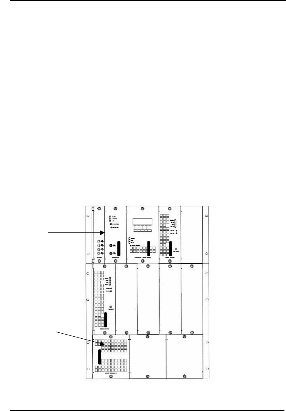
shown in Figure 2-1.
The LL50ATC transmitter operates at a
nominal output power of 50 watts digital.
Typically with a 36 MHz COFDM
(orthogonal frequency division
multiplexing) IF input the transmitter
produces an RF on channel 1.67 MHz
output.
The model number scheme for a
Innovator LX Series digital transmitter is
as follows (where ### = power in
watts):
LL####ATC - Low power, L-Band, ###
Single Output, A-Line, Transmitter,
COFDM
(Example):
LL50ATC is a 50-Watt Single Output
Digital 1.67 GHz Transmitter using the
Orthogonal Frequency Division
Multiplexing modulation scheme.
The modules and assemblies that make
up the Exciter/driver chassis assembly
are shown in Figure 2-2 and listed in
Table 2-1.
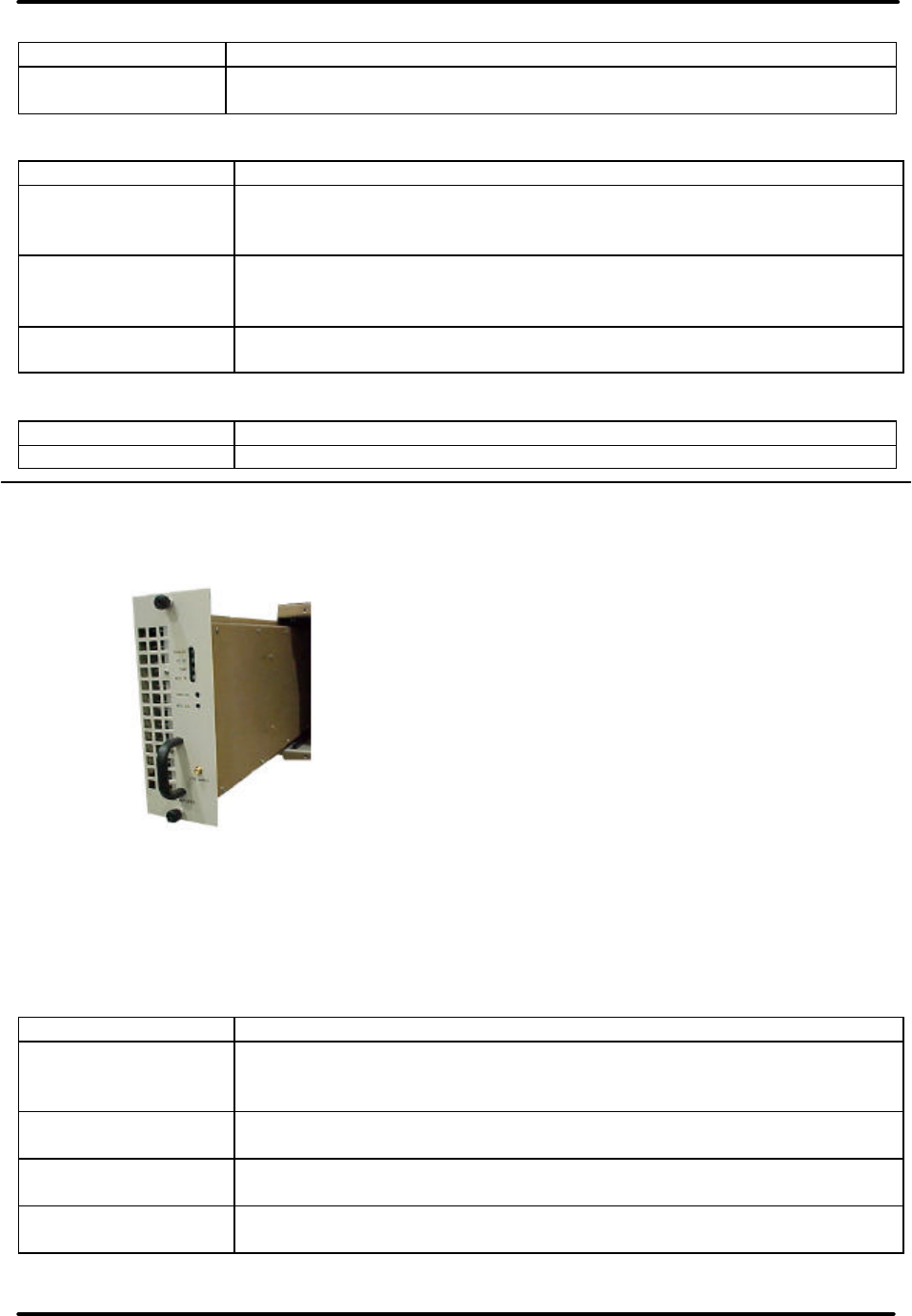
Figure 2-1: LL50ATC Front View
Single
Exciter/Driver
Chassis
Assembly
LL50
ATC Power
Amplifier
Chassis
Assembly
1.67 GHz 50 Watt Single Output Transmitter Chapter 2, System Description
LL50ATC, Rev. 0 2-2
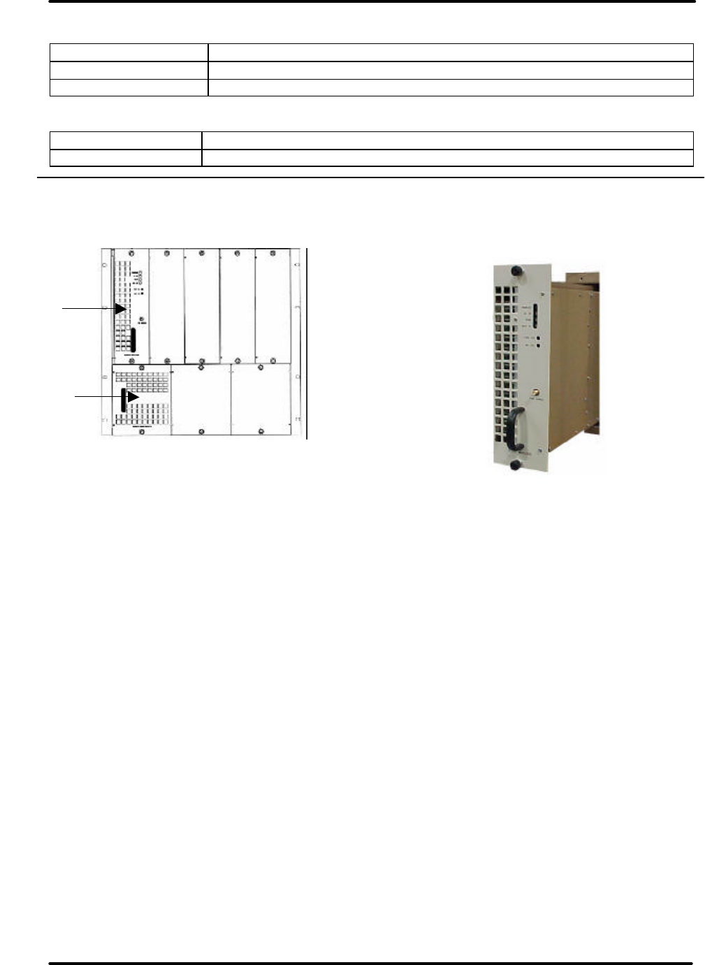
Figure 2-2: Exciter/Driver Chassis, Single, 1.67 GHz, Front View
Table 2-1: Exciter/Driver, 1.67 GHz, Modules and Assemblies
ASSEMBLY DESIGNATOR TRAY/ASSEMBLY NAME PART NUMBER
Exciter Amplifier Chassis
Assembly, Single, 1.67 GHz 1305021 (220 VAC)
A1 Metering Module 1304976
A2 Upconverter Module, Single 1305061
A4 Control/Power Supply Module 1305035 (220 VAC)
A6 5 Watt Driver Amplifier Module 1304844
A11 Backplane Board, 1.67 GHz 1304891
2.1 Exciter Amplifier Chassis
Assembly, Single, 1.67 GHz, 220 VAC
(1305021); Appendix B
The chassis assembly provides the area
in which the Modules are mounted. The
Metering and the Upconverter Modules
slide into the assembly and plug directly
into the backplane board. The driver
power amplifier module and the power
supply section of the Control &
Monitoring/Power Supply Module also
slide into the assembly but do not plug
directly into the backplane board. The
backplane board provides module to
module interconnection as well as
interconnection to remote command and
control connectors. Refer to the chassis
interconnect drawing (1305023) and the
backplane board schematic drawing
(1304893), located in Appendix B, for the
exciter amplifier chassis assembly
connections.
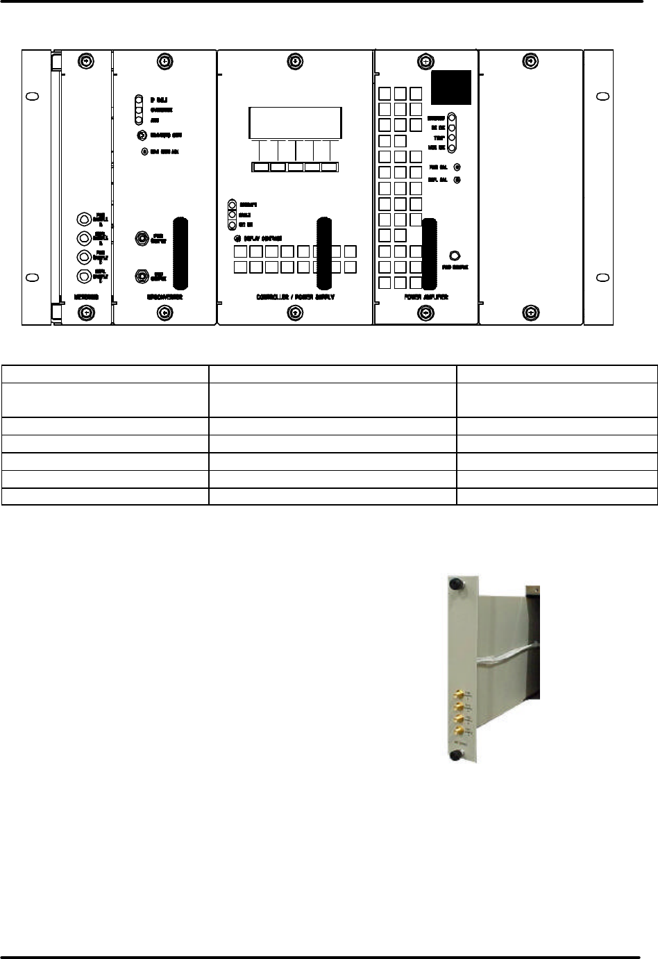
2.1.1 (A1) Metering Assembly, 1.67
GHz (1304976; Appendix B)
The (A1) Metering Assembly contains the
Metering Board, 1.67 GHz (1304922).
This assembly has circuitry that is used
to measure the average power of up to
four RF inputs. Each RF input is split on
the Metering Board, with some of the
signal being applied to an average
power detector, and the rest of the
A2
A4
A6
A1
1.67 GHz 50 Watt Single Output Transmitter Chapter 2, System Description
LL50ATC, Rev. 0 2-3
signal sent to the front panel sample to
allow the operator to monitor the RF
signal with his own test equipment. The
output of each detector is sent to the
transmitter's system control via the
Backplane board into which the
assembly plugs.
Table 2-2. Metering Assembly Front Panel Samples
SMA CONNECTOR DESCRIPTION
FWD SAMPLE A Sample of A Output Power
REFL SMAPLE A Sample of A Reflected Power
FWD SAMPLE B Sample of B Output Power
REFL SMAPLE B Sample of B Reflected Power
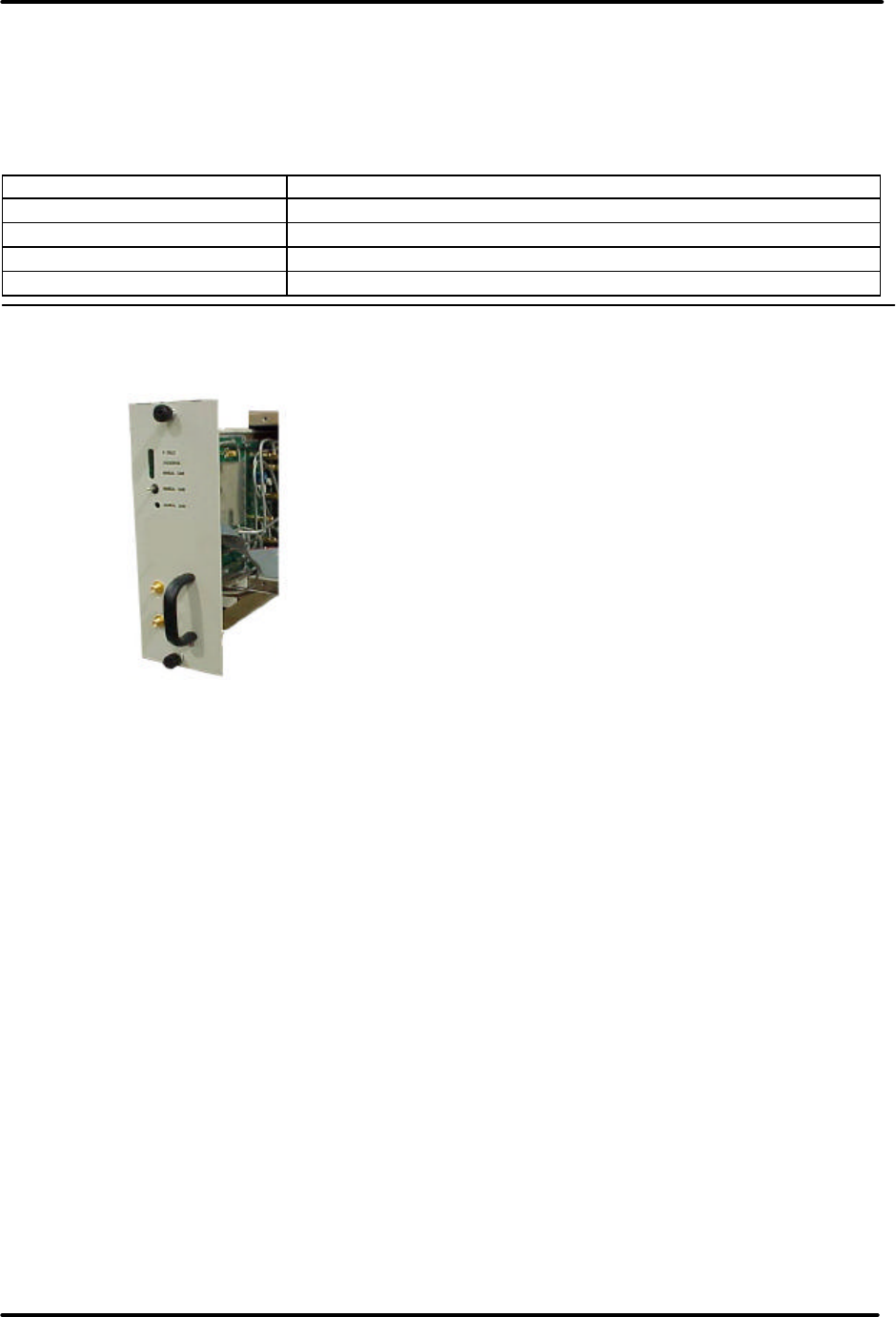
2.1.2 (A2) Upconverter Module
Assembly (1305061; Appendix B)
The Upconverter Module Assembly
contains an Upconverter Control board
(1304780), an LO Generator board
(1304940) and either one or two
Upconverter boards (1304929).
This assembly converts either one or
two separate 36 MHz IF signals to either
one or two RF outputs at a frequency of
1670-1675 MHz.
The description below is for one half of
the upconverter assembly. The IF and
upconverter paths can be duplicated to
provide two outputs when needed. The
second IF path is always present, but
not used in single output upconverters.
A second Upconverter board is added for
dual output transmitters.
An IF Signal centered at 36 MHz at a
level of 0 dBm average is applied to the
Upconverter Control board. A sample is
applied to a peak detector, which checks
for the presence of an IF input. If the
input is not present, an alarm is
generated and displayed on the
module's front panel, and is also noted
by the microcontroller on the
Upconverter control board. The IF
signal is then applied to a pin diode
attenuator, which is used to hold the
output level of the transmitter constant.
The signal then is applied to the
Upconverter board, and converted to RF
via a double balanced mixer. The
resulting RF output signal is filtered,
then amplified, and is sent back to the
Upconverter Control board, which routes
it to the back of the tray. There is also a
second output -20dB from the main
output that is sent to the front panel as
a sample.
The local oscillator consists of a Crystal
oscillator running at 1/15 of the final LO
frequency of 1708.5 MHz. The oscillator
drives a X5 multiplier, is filtered, and
then is sent to a final X3 multiplier
circuit. A sample of the output signal is
applied to a PLL circuit, which locks the
LO signal to a 10 MHz reference
generated by the Upconverter Control
Board. An alarm is generated if the PLL
unlocks that is sent to a microcontroller
on the Upconverter Control Board. There
are two outputs that are sent to the two
upconverter control boards, and a third
output used as a front panel LO sample.
The LO generator board also contains all
the front panel alarms and controls. In
addition to the Input Fault indicator
mentioned above, there is also an
indicator that shows the status of the
Overdrive detection circuit, and another
1.67 GHz 50 Watt Single Output Transmitter Chapter 2, System Description
LL50ATC, Rev. 0 2-4
indicator that shows the status of the
AGC circuit.
The AGC circuit is located on the
upconverter control board, and attempts
to adjust the gain of the IF pin
attenuator to hold a constant output
power. The circuit also looks at the
output power of the driver, and will limit
how far the pin attenuator can adjust if
the output power of the driver gets to
high. When it does so, the Overdrive
indicator switches from green to Red.
The status of the AGC circuit is
controlled by a front panel switch, which
can bypass the AGC and operate the pin
attenuator with a fixed bias instead of
with the AGC circuit. The indicator is
normally green when the AGC circuit is
enabled, and switches to Amber if the
AGC switch is in manual.
Table 2-3. Upconverter Front Panel Switch
SWITCH FUNCTION
MAN/AUTO AGC
(Left Manual, Right AGC) Controls AGC function. Switched to left bypasses AGC.
Table 2-4. Upconverter Front Panel Status Indicators
LED FUNCTION
Input Fault
(Red) When lit it indicates that the input is missing or the level is below
the preset value.
AGC Overdrive
(Red) When lit it indicates that the AGC is cutting back due to too much
drive to the driver module.
AGC Fault
(Red) When lit it indicates that the AGC is out of range.
Table 2-5. Upconverter Front Panel Control Adjustments
POTENTIOMETERS DESCRIPTION
MAN GAIN ADJ Adjusts the gain of the upconverter and transmitter when in the
Manual AGC position.
Table 2-6. Upconverter Front Panel Samples
SMA CONNECTOR DESCRIPTION
FWD SAMPLE Sample of the RF Output of the Upconverter
OSC SAMPLE Sample of the LO signal in the Upconverter as generated on the LO
Generator Board.
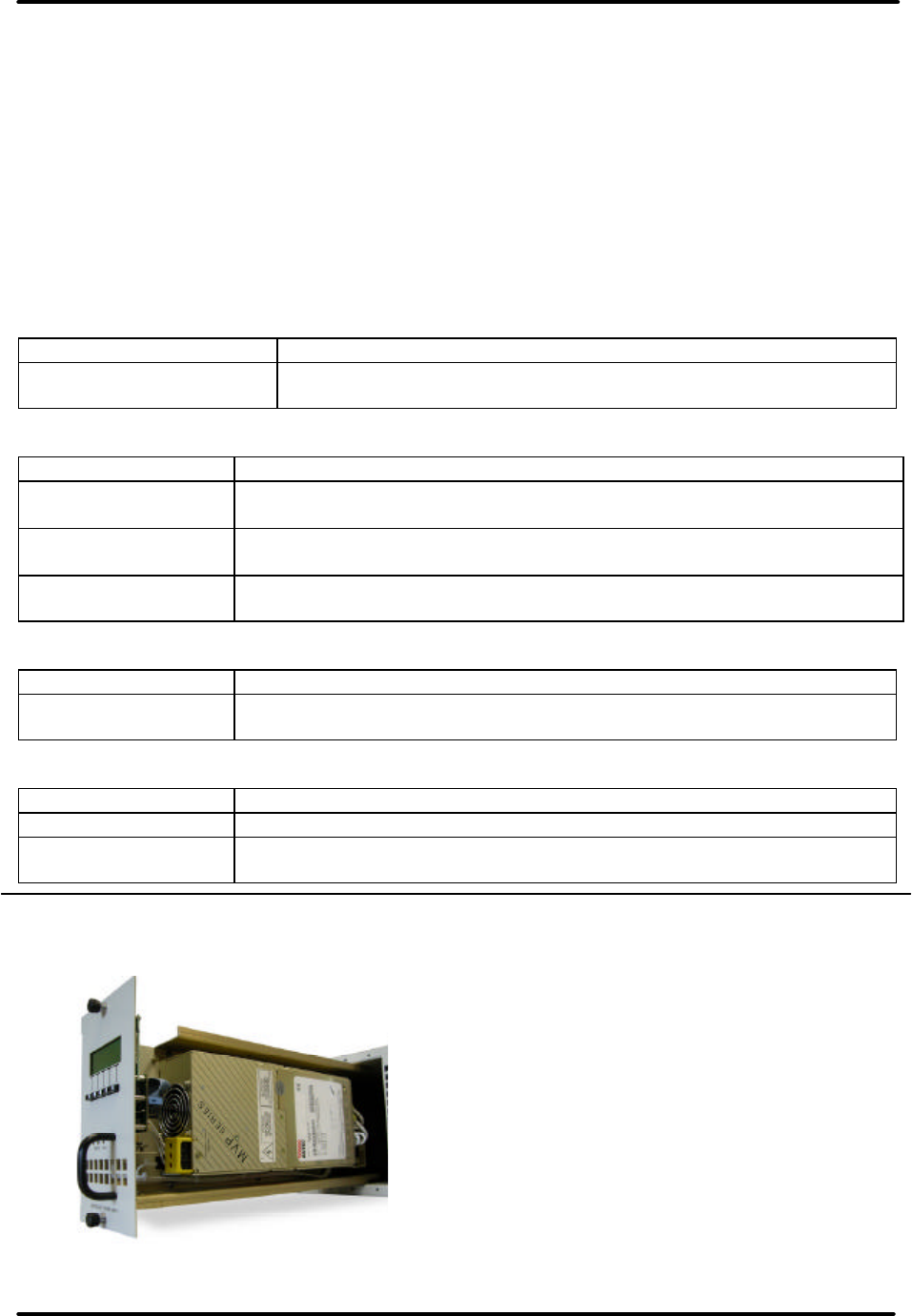
2.1.3 (A4) Control/Power Supply
Module Assembly, 220 VAC
(1305035; Appendix B)
The Control & Monitoring/Power Supply
Assembly is made up of a Control Board
(1302021), a Power Protection Board
(1302837) and a Switch Board (1527-
1406). The Assembly also contains a
switching power supply that provides ±12
VDC to the rest of the modules in the
chassis and +28 VDC to the Power
Amplifier module.
The Assembly provides all transmitter
control and monitoring functions. The
Front panel LCD allows monitoring of
system parameters, including forward
and reflected power, transistor currents,
module temperatures and power supply
voltages.
1.67 GHz 50 Watt Single Output Transmitter Chapter 2, System Description
LL50ATC, Rev. 0 2-5
Table 2-7. Controller/Power Supply Display
DISPLAY FUNCTION
LCD A 4 x 20 display providing a four-line readout of the internal
functions, external inputs, and status.
Table 2-8. Controller/Power Supply Status Indicator
LED FUNCTION
OPERATE
(green)
When lit it indicates that the transmitter is in the Operate Mode. If
transmitter is Muted the Operate LED will stay lit, the transmitter
will remain in Operate, until the input signal is returned.
FAULT
(red or green)
Red indicates that a problem has occurred in the transmitter. The
transmitter will be Muted or placed in Standby until the problem is
corrected.
DC OK
(red or green) Green indicates that the switchable fuse protected DC outputs that
connect to the modules in the transmitter are OK.
Table 2-9. Controller/Power Supply Control Adjustments
POTENTIOMETERS DESCRIPTION
DISPLAY CONTRAST Adjusts the contrast of the display for desired viewing of screen.
2.1.4 (A6) 5 Watt Driver Power
Amplifier Assembly (1304844;
Appendix B)
The 5 Watt Driver PA assembly consists
of an amplifier control board (1304774)
and a two stage 40 Watt Driver board
(1304865). The assembly amplifies the
output from the upconverter assembly
to a power level of 1 to 5W average
power.
The amplifier has two stages of gain,
both of them using LDMOS transistors
operating from a +28V supply. The
amplifier control board monitors the
driver PA assemblies output and
reflected power, temperature, and the
current drawn from the two devices.
A sample of the output signal is routed
to the front panel for monitoring
purposes. There are also two controls
on the front panel used to calibrate the
metering of the forward and reflected
power of the driver assembly.
Table 2-10. 5 Watt Driver Power Amplifier Status Indicators
LED FUNCTION
ENABLED
(Green)
When lit Green, it indicates that the PA is in the Operate Mode. If a
Mute occurs, the PA will remain Enabled, until the input signal is
returned.
DC OK
(Green) When lit Green, it indicates that the fuse protected DC inputs to the
PA module are OK.
TEMP
(Green) When lit Green, it indicates that the temperature of the heatsink
assembly in the module is below 78°C.
MOD OK
(Green) When lit Green, it indicates that the PA Module is operating and has
no faults.
1.67 GHz 50 Watt Single Output Transmitter Chapter 2, System Description
LL50ATC, Rev. 0 2-6
Table 2-11. 5 Watt Driver Power Amplifier Status Adjustments
POTENTIOMETERS DESCRIPTION
FORWARD CAL Adjusts the gain of the Forward Power monitoring circuit
RFL CAL Adjusts the gain of the Reflected Power monitoring circuit
Table 2-12. 5 Watt Driver Power Amplifier Status Indicators
DISPLAY FUNCTION
FWD SAMPLE RF sample of the amplified signal being sent out the module on J25.
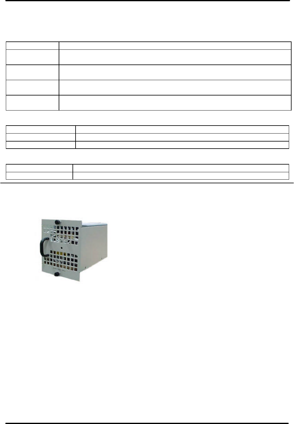
2.2 Power Amplifier Chassis
Assembly, LL50ATC (1305863;
Appendix B)
The power amplifier chassis assembly in
the LX Series contains a modular
television amplifier that slides into the
assembly that produces approximately
50-Watts Digital output. There is also
needed an external Power Supply Module
Assembly, which also slides into the
Power Amplifier Chassis Assembly, under
the PA Module.
The RF output of the exciter/driver at the
“N” connector J8 connects to the (A3)
power amplifier chassis assembly at the
“N” connector J201. Data and control
information for the system is fed through
the system serial cable. The system
serial cable connects from J34 on the
exciter/driver assembly to J232 on the
Power Amplifier Assembly that connects
to (A4) the External Amplifier Signal
Board (1303344).
The RF input at J201 is connected to
J111 on the power amplifier module. The
output of the power amplifier at J112
connects to the RF output jack J203 of
the power amplifier chassis assembly.
2.2.1 (A3) Power Amplifier Module
Assembly, 100 Watt, 1/67 GHz
(1304502; Appendix B)
The 100W amplifier assembly consists of
an amplifier module control board
(1304774), a single stage driver board
(1304616), a phase/gain board
(1305026) and a Quad Stage board
(1304607). The assembly amplifies the
output from the upconverter assembly
to a power level of 1 to 5 Watts average
power.
The amplifier has two stages of gain,
both of them LDMOS transistors
operating from a +28V supply. The
output stage consists of four LDMOS
devices operating in parallel, combined
with quadrate hybrids. The amplifier
control board monitors the assemblies’
output and reflected power,
temperature, and the current drawn
from the driver, and each pair of output
devices.
A sample of the output signal is routed
to the front panel for monitoring
purposes.
100 Watt
PA
Assembly
Power
Supply
Assembly
1.67 GHz 50 Watt Single Output Transmitter Chapter 2, System Description
LL50ATC, Rev. 0 2-7
There are also two controls on the front
panel used to calibrate the metering of the forward and reflected power of the
PA assembly.
Table 2-13. Power Amplifier Status Indicators
LED FUNCTION
ENABLED
(Green) When lit Green, it indicates that the PA is in the Operate Mode. If a Mute
occurs, the PA will remain Enabled, until the input signal is returned.
DC OK
(Green) When lit Green, it indicates that the fuse protected DC inputs to the PA
module are OK.
TEMP
(Green) When lit Green, it indicates that the temperature of the heatsink
assembly in the module is below 78°C.
MOD OK
(Green) When lit Green, it indicates that the PA Module is operating and has no
faults.
Table 2-14. Power Amplifier Control Adjustments
POTENTIOMETERS DESCRIPTION
RFL CAL Adjusts the gain of the Reflected Power monitoring circuit
FORWARD CAL Adjusts the gain of the Forward Power monitoring circuit
Table 2-15. Power Amplifier Sample
DISPLAY FUNCTION
FWD SAMPLE RF sample of the amplified signal being sent out the module on J25.
2.1.4 Power Supply Module
Assembly, 1 kW
(1305174; Appendix B)
The Power Supply Module Assembly is
made up of a +28V/2000W Switching
Power Supply and a ±12V/40W Switching
Power Supply.
The power supply module provides the
+28 VDC and the +12 VDC and -12 VDC
to the power amplifier module assembly.
2.1.5 RF Output Assemblies
The 36 MHz COFDM Modulated IF from
the PROTV modulator connects to the
rear of the exciter/driver chassis
assembly at J24, the RF input jack. The
driver power amplifier RF output jack is
at the “N” connector J25, PA RF Output.
The RF output of the driver PA module is
connected directly to the input of the
power amplifier assembly. The PA
assembly amplifies the RF signal to
approximately 100W. The output is
connected to a coupler assembly, which
provides forward and reflected samples
of the transmitters DTV output signal,
before it is filtered for testing purposes.
The output of the coupler is connected
to a Myat 1.67 GHz 8 Section Bandpass
Filter. The filter is tuned to a 5 MHz
bandwidth around 1.6725 MHz center
frequency.
The filtered signal is next connected to a
low pass filter and output coupler
assembly. The output coupler assembly
provides a forward and a reflected
power sample to the Metering Board,
mounted in the exciter/driver assembly
cabinet, for metering and test purposes.
The RF output of the transmitter is at
the “N” connector output jack of the low
pass filter output coupler assembly.

1.67 GHz 50 Watt Single Output Transmitter Chapter 2, System Description
LL50ATC, Rev. 0 2-8
2.2 Control and Status
The control and status readings of the
exciter/driver chassis assembly are
found by operating the front panel
display screen on the front of the
assembly.
2.2.1 Front Panel Display Screens
A 4 x 20 display located on the front of
the Control & Monitoring/Power Supply
Module is used in the LX Series
transmitter for control of the operation
and display of the operating parameters
of the transmitter.
2.3 System Operation
When the transmitter is in operate, as set
by the menu screen located on the
Control & Monitoring Module, the
following occurs. The +28 VDC stage of
the Power Supply in the Control &
Monitoring Module is enabled, the
operate indicator on the front panel is lit
and the DC OK on the front panel should
also be green. The enable and DC OK
indicators on the driver PA Module will
also be green.
When the transmitter is in standby. The
+28 VDC stage of the Power Supply in
the Control & Monitoring Module is
disabled, the operate indicator on the
front panel will be extinguished and the
DC OK on the front panel should remain
green. The enable indicator on the driver
PA Module is also extinguished.
If the transmitter does not switch to
Operate when the operate menu is
switched to Operate, check that all faults
are cleared and that the remote control
terminal block stand-by signal is not
active.
2.3.1 Principles of Operation
Operating Modes
This transmitter is either operating or in
standby mode. The sections below
discuss the characteristics of each of
these modes.
Operate Mode
Operate mode is the normal mode for
the transmitter when it is providing RF
power output. To provide RF power to
the output, the transmitter will not be in
mute. Mute is a special case of the
operate mode where the +28 VDC
section of the power supply is enabled
but there is no RF output power from
the transmitter.
Operate Mode with Mute Condition
The transmitter will remain in the
operate mode but will be placed in mute
when the following fault conditions
exists in the transmitter.
• Upconverter is unlocked
• Upconverter module is not present
Entering Operate Mode
Entering the operate mode can be
initiated a few different ways by the
transmitter control board. A list of the
actions that cause the operate mode to
be entered is given below:
• A low on the Remote Transmitter
Operate line.
• User selects "OPR" using switches
and menus of the front panel.
• Receipt of an “Operate CMD” over
the serial interface.
There are several fault or interlock
conditions that may exist in the
transmitter that will prevent the
transmitter from entering the operate
mode. These conditions are:
• Power Amplifier heat sink
temperature greater than 78°C.
• Transmitter is Muted due to
conditions listed above.

1.67 GHz 50 Watt Single Output Transmitter Chapter 2, System Description
LL50ATC, Rev. 0 2-9
• Power Amplifier Interlock is high
indicating that the amplifier is not
installed.
Standby Mode
The standby mode in the transmitter
indicates that the output amplifier of the
transmitter is disabled.
Entering Standby Mode
Similar to the operate mode, the
standby mode is entered using various
means. These are:
• A low on the Remote Transmitter
Stand-By line.
• Depressing the “STB” key on
selected front panel menus.
• Receipt of a “Standby CMD” over the
serial interface.
RF System Interlock
A RF System Interlock signal is provided
through TB30-5. When this signal's
circuit is completed to ground such as
through a wire between TB30-5 and
TB30-15, the transmitter is allowed to
operate. If this circuit is opened, the
transmitter switches to a Mute condition.
This circuit may be completed through
coax relay contacts and reject load
contact closures to assure the RF output
system is available to receive the
transmitter's output RF signal.
2.4 Maintenance
The Innovator LX Series Transmitter is
designed with components that require
little or no periodic maintenance except
for the routine cleaning of the fans and
the front panels of the modules. The
amount of time between cleanings
depends on the conditions within the
transmitter room. While the electronics
have been designed to function even if
covered with dust, a heavy buildup of
dust, dirt, or insects will affect the
cooling of the components. This could
lead to a thermal shutdown or the
premature failure of the affected module.
When the front panels of the modules
become dust covered, the module should
be pulled out and any accumulated
foreign material should be removed.
NOTE: To remove the driver/power
amplifier module, mounted in the
exciter/driver assembly, the input and
output cables must be removed from the
rear of the module and also a 6/32” x ½”
Philips screw, mounted between the two
connectors, needs to be removed before
the module will pull out. After removal of
the screw, which is used to hold the
module in place during shipping, it does
not need to be replaced.
A vacuum cleaner, utilizing a small,
wand-type attachment, is an excellent
way to suction out the dirt. Alcohol and
other cleaning agents should not be used
unless you are certain that the solvents
will not damage components or the silk-
screened markings on the modules and
boards. Water-based cleaners can be
used, but do not saturate the
components. The fans and heatsinks
should be cleaned of all dust or dirt to
permit the free flow of air for cooling
purposes.
It is recommended that the operating
parameters of the driver/transmitter be
recorded from the LEDs on the modules
and the LCD system metering on the
control/monitoring module at least once
a month. It is suggested that this data be
retained in a rugged folder or envelope.
2.5 Customer Remote Connections
The remote monitoring and operation of
the transmitter is provided through jack
TB30 located on the rear of the chassis
assembly. If remote connections are
made to the transmitter, they must be
made through plug TB30 at positions
noted on the transmitter interconnect
drawing and in Table 2-16.
1.67 GHz 50 Watt Single Output Transmitter Chapter 2, System Description
LL50ATC, Rev. 0 2-10
Figure 2-3. Exciter/Driver Chassis Assembly Rear View
Table 2-16: LX Series Chassis Assembly Hard Wired Remote Interface Connections to
TB30 an 18 pos. Terminal Block Located on the Rear of the Assembly
Signal Name Pin
Designations Signal Type/Description
RMT Transmitter
State TB30-1 Discrete Open Collector Output - A low indicates
that the transmitter is in the operate mode.
RMT Transmitter
Interlock TB30-2
Discrete Open Collector Output - A low indicated
the transmitter is OK or completes a interlock daisy
chain. When the transmitter is not faulted, the
interlock circuit is completed.
RMT Transmitter
Interlock Isolated
Return TB30-3
Ground - Configurable ground return which can be
either jumpered directly to ground or it can be the
“source” pin of an FET so that the transmitter
interlock can be daisy chained with other
transmitters. This signal does not directly interface
to the microcontroller.
RMT AUX IO 1 TB30-4
Discrete Open Collector Inputs, Discrete Open
Drain Outputs, or 0 - 5 VDC Analog Input - When
used as an output, this line is pulled to +5 VDC
with a 1.0 kO resistor for logic high and pulled to
ground for a low. A diode allows this line to be
pulled up to 12 VDC. When used as a digital input,
this line considers all values over 2 Volts as high
and those under 1 volt as low. As an analog input,
this line is protected by a 5.1 zener diode.
RMT AUX IO 2 TB30-5 Same as RMT AUX IO 1.
RMT
Transmitter
Operate CMD TB30-7 Discrete Open Collector Input - A pull down to
ground on this line indicates that the transmitter is
to be placed into the operate mode.
RMT
Transmitter
Stand-By CMD TB30-9
Discrete Open Collector Input - A pull down to
ground on this line indicates that the transmitter is
to be placed into the standby mode.
TB30

1.67 GHz 50 Watt Single Output Transmitter Chapter 2, System Description
LL50ATC, Rev. 0 2-11
Signal Name Pin
Designations Signal Type/Description
RMT
RF System
Interlock A TB30-11
When this signal's circuit is completed to ground
such as through a wire between TB30-11 and
TB30-12, the transmitter A is allowed to operate.
If this circuit is opened, transmitter A switches to a
Mute condition.
RMT
RF System
Interlock B
(Used in dual
systems only)
TB30-13
When this signal's circuit is completed to ground
such as through a wire between TB30-13 and
TB30-14, transmitter B is allowed to operate. If
this circuit is opened, transmitter B switches to a
Mute condition.
RMT Ground TB30-6, 8, 10,
12, 14, 16, and
18 Ground pins available through Remote
RMT +12 VDC TB30-15 +12 VDC available through Remote w/ 2 Amp re-
settable fuse
RMT -12 VDC TB30-17 -12 VDC available through Remote w/ 2 Amp re-
settable fuse

1.67 GHz 50 Watt Single Output Transmitter Chapter 3, Circuit Descriptions
LL50ATC, Rev. 0 3-1
Chapter 3
Circuit Descriptions
3.1 (A1) Metering Module Assembly
(1304976; Appendix B)
This assembly has circuitry that is used
to measure the average power of up to
four RF inputs. Each RF input is split on
the Metering Board, with some of the
signal being applied to an average
power detector, and the rest of the
signal sent to the front panel sample to
allow the operator to monitor the RF
signal with his own test equipment. The
output of each detector is sent to the
transmitter's system control via the
Backplane board into which the
assembly plugs.
The Metering Assembly contains the
Metering Board, 1.67 GHz (1304922).
3.1.1 Metering Board (1304922;
Appendix B)
This board has circuitry that is used to
measure the average power of up to
four RF inputs that come in to the board
at the mixed signal connector J1. Each
RF input is split with some of the signal
being applied to one of the average
power detector ICs on the board (U2,
U4, U5, and U7), and the rest of the
signal is sent to the front panel as a
sample to allow the operator to monitor
the RF signal with his own test
equipment. The output of each detector
is sent to the transmitter's system
control via J1 to the Backplane that the
assembly plugs into. Each section has a
calibration pot that is factory set (R5,
R15, R25, R35).
3.2 (A2) Upconverter Module
Assembly, Single Output (1305061;
Appendix B)
This assembly converts the 36 MHz IF
input signal to the RF output at a
frequency of 1670-1675 MHz.
The Upconverter Module Assembly contains
an Upconverter Control board (1304780),
an LO Generator board (1304940) and the
Upconverter board (1304929).
3.2.1 (A1) Upconverter Control Board
(1304780; Appendix B)
An IF Signal centered at 36 MHz at a level
of 0 dBm average is applied to J1-11B of
the Upconverter Control board. A sample
is connected to a peak detector, which
checks for the presence of the IF input. If
the input is not present, an alarm is
generated and displayed on the module's
front panel, and is also noted by
microcontroller U20 on the Upconverter
control board. The IF signal is then
applied to a pin diode attenuator, which is
used to hold the output level of the
transmitter constant.
The AGC circuit is located on the
upconverter control board, and attempts
to adjust the gain of the IF pin attenuator
to hold a constant output power. The
circuit also looks at the output power of
the driver, and will limit how far the pin
attenuator can adjust if the output power
of the driver reaches too high a level.
When it does so, the Overdrive indicator
switches from Green to Red. The status
of the AGC circuit is controlled by a front
panel switch, which can bypass the AGC,
and operate the pin attenuator with a
fixed bias instead of with the AGC circuit.
The indicator is normally Green when the
AGC circuit is enabled, and switches to
Amber if the AGC switch is in manual.
This information is fed back to the
Upconverter control board and used to
control the AGC.
There is a second IF and AGC path for the
B side of the transmitter if it is present.
Its operation is identical to side A just
described.

1.67 GHz 50 Watt Single Output Transmitter Chapter 3, Circuit Descriptions
LL50ATC, Rev. 0 3-1
The board also controls what 10 MHz
reference is used by the PLL circuitry of
the Upconverter. In normal operation
the board uses an external 10 MHz
reference, which enters the board at J1-
5B. Its presence is detected with a peak
detector that controls a relay. If the
external reference is not present, the
board switches over to its internal
reference U2. This reference is not
suitable for use in a transmitter with an
SFN network as the transmitter will no
longer be locked to the GPS, but it does
allow the transmitter to be tested
without requiring a GPS reference.
Microcontroller U20 performs all the
data collection and reporting functions
for the Upconverter. It communicates
via an RS-485 link to the transmitter's
system controller.
3.2.2 (A1) Upconverter Board,
1.67 GHz (1304929; Appendix B)
This board converts a 36 MHz IF input to
a 1672.5 MHz RF output.
The IF input at J2 passes through a
frequency response correction circuit,
consisting of adjustments C8, C9, R6
and R7, which are factory set to
compensate for any response variation
in the upconverter assembly. The signal
is then converted to the final frequency
by a double balanced mixer U4.
The RF output of the mixer amplified by
U5 and filtered by the band pass filter
U7 and amplified by U8 before it is
connected to J7 on the board. A coaxial
cable jumper connects J7 to J4 on the
board. The RF is filtered by a second
band pass filter U13 and amplified by U9
and U10. The output is then sent to the
directional coupler U11 and exits the
board at the RF output jack J5
The coupled output from U11 leaves the
board at the SMA J6, which is accessed
through the front panel of the
Upconverter Assembly, for monitoring
purposes.
3.2.3 (A4) LO Generator Board, Single
Output (1305829; Appendix B)
The local oscillator consists of a Crystal
oscillator consisting of Y1, Q2 and their
associated components running at 1/15 of
the final LO frequency of 1708.5 MHz.
The oscillator drives a X5 multiplier
consisting of CR1, L3, and L6-L8. The
output is filtered and then is sent to a final
X3 multiplier circuit consisting of CR2, C22
and C23. The output is filtered by the
band pass filter U5 and then split by the
splitter U7. A sample of the output signal
is applied to the PLL circuit U11, which
locks the LO signal to a 10 MHz reference
generated by the Upconverter Control
Board. An alarm is generated if the PLL
unlocks that is applied to a microcontroller
on the Upconverter Control Board. In a
dual system, there are two outputs that
are sent to the two upconverter control
boards, and a third output used as a front
panel LO sample. There is only one
upconverter board in a single system
The LO generator board also contains all
of the front panel alarms and controls.
There are LED indicators that show, the
status of the IF input, the status of the
Overdrive detection circuit, and another
indicator that shows the status of the AGC
circuit.
The external AGC circuit is located on the
upconverter control board, and attempts
to adjust the gain of the IF pin attenuator
to hold a constant output power. The
circuit also looks at the output power of
the driver, and will limit how far the pin
attenuator can adjust if the output power
of the driver increases too much. When it
gets too high, the Overdrive indicator
switches from Green to Red. The status
of the AGC circuit is controlled by a front
panel switch, which can bypass the AGC.
When bypassed the pin attenuator is
controlled by a fixed bias instead of with
the AGC circuit. The indicator is normally
Green when the AGC circuit is enabled,
and switches to Amber when the AGC
switch is in manual.

1.67 GHz 50 Watt Single Output Transmitter Chapter 3, Circuit Descriptions
LL50ATC, Rev. 0 3-2
3.3 (A4) Control Monitoring/Power
Supply Module, 220 VAC
(1305035;Appendix B)
The Control Monitoring/Power Supply
Module Assembly contains (A1) a Power
Protection Board (1302837), (A2) a 600
Watt Switching Power Supply, (A3) a
Control Board (1302021), (A4) a Switch
Board (1527-1406) and (A5) a LCD
Display.
AC Input to Exciter/Driver Chassis
Assembly
The AC input to the Exciter/Driver
Chassis Assembly is connected from J12,
part of a fused entry module, located on
the rear of the chassis assembly to J50
on the Control Monitoring/Power Supply
Module. J50-10 is line #1 input, J50-8 is
earth ground and J50-9 is neutral input.
The input AC connects to J1 on the Power
Protection Board where it is fuse
protected and connected back to J50, at
J50-11 AC Line #1 and J50-12 AC Line
#2, for distribution to the cooling Fan.
3.3.1 (A1) Power Protection Board
(1302837; Appendix B)
The input AC connects through J1 to two
10 Amp AC fuses F1 and F2. The AC
line #1 input connects from J1-1 to the
F1 fuse. The AC line #1 input after the
F1 fuse is split with one line connected
back to Jack J1 Pin 4, which becomes
the AC Line #1 to the Fan. The other
line of the split connects to J4. The AC
line #2 input connects from J1-3 to the
F2 fuse. The AC line #2 input after the
F2 fuse is split with one line connected
back to Jack J1 at Pin 5, which becomes
the AC Line #2 to the Fan. The other
line of the split connects to J2. J1-2 is
the earth ground input for the AC and
connects to J3.
Three 150 VAC, for 115 VAC input, or
three 275 VAC, for 230 VAC input, MOVs
are connected to the input AC for
protection. One connects from each AC
line to ground and one connects across
the two lines. VR1 connects from J4 to J2,
VR2 connects from J4 to J3 and VR3
connects from J2 to J3.
3.3.1.1 +12 VDC Circuits
+12 VDC from the Switching Power
Supply Assembly connects to J6 on the
board. The +12 VDC is divided into four
separate circuits each with a 3 amp self
resetting fuse, PS3, PS4, PS5 and PS6.
The polyswitch resettable fuses may open
on a current as low as 2.43 Amps at
50°C, 3 Amps at 25°C or 3.3 Amps at
0°C. They definitely will open when the
current is 4.86 Amps at 50°C, 6 Amps at
25°C or 6.6 Amps at 0°C.
PS3 protects the +12 VDC 2 Amp circuits
for the System Controller, the Amplifier
Controller and the Spare Slot through J62
pins 7, 8, 9 and 10. If this circuit is
operational, the Green LED DS3, mounted
on the board, will be lit.
PS4 protects the +12 VDC 2 Amp circuits
for the Modulator and the IF Processor
through J62 pins 13, 14, 15 and 16. If
this circuit is operational, the Green LED
DS4, mounted on the board, will be lit
PS5 protects the +12 VDC 2 Amp circuits
for the Upconverter through J62 pins 17,
18, 19 and 20. If this circuit is
operational, the Green LED DS5, mounted
on the board, will be lit
PS6 protects the +12 VDC 2 Amp circuits
for the Remote through J63 pins 17, 18,
19 and 20. If this circuit is operational,
the Green LED DS6, mounted on the
board, will be lit
3.3.1.2 -12 VDC Circuits
-12 VDC from the Switching Power Supply
Assembly connects to J5 on the board.
The -12 VDC is divided into two separate
circuits each with a 3 amp self-resetting
fuse, PS1 and PS2.

1.67 GHz 50 Watt Single Output Transmitter Chapter 3, Circuit Descriptions
LL50ATC, Rev. 0 3-3
PS1 protects the -12 VDC 2 Amp circuits
for the System through J63 pins 1, 2, 3
and 4. If this circuit is operational, the
Green LED DS1, mounted on the board,
will be lit
PS2 protects the -12 VDC 2 Amp circuits
for the Remote through J62 pins 1, 2, 3
and 4. If this circuit is operational, the
Green LED DS2, mounted on the board,
will be lit
The connections from J62 and J63 of the
Power Protection Board are wired to J62
and J63 on the Control Board.
3.3.2 (A3) Control Board (1302021;
Appendix B)
In this transmitter, control monitoring
functions and front panel operator
interfaces are found on the Control
Board. Front panel operator interfaces
are brought to the control board using a
26-position conductor ribbon cable that
plugs into J60. The control board
controls and monitors the Power Supply
and Power Amplifier module through a
16 position connector J61 and two 20
position connectors J62 & J63.
3.3.2.1 Schematic Page 1
U1 is an 8 bit RISC microcontroller that
is in circuit programmed or programmed
using the serial programming port J4 on
the board. When the microcontroller,
U1, is held in reset, low on pin 20, by
either the programming port or the
external watchdog IC (U2), a FET Q1
inverts the reset signal to a high that
connects to the control lines of U5, an
analog switch. The closed contacts of
U5 connects the serial programming
lines from J4 to U1. LED DS10 will be lit
when programming port J4 is used.
U2 is a watchdog IC used to hold the
microcontroller in reset, if the supply
voltage is less the 4.21 VDC; (1.25 VDC
< Pin 4 (IN) < Pin 2 (Vcc). The
watchdog momentarily resets the
microcontroller, if Pin 6 (ST) is not
clocked every second. A manual reset
switch S1 is provided but should not be
needed.
Diodes DS1 through DS8 are used for
display of auto test results. A test board
is used to execute self-test routines.
When the test board is installed,
Auto_Test_1 is held low and Auto_Test_2
is allowed to float at 5 VDC. This is the
signal to start the auto test routines.
U3 and U4 are used to selectively enable
various input and output ICs found on
pages 2 & 3 of the schematic.
U1 has two serial ports available. In this
application, one port is used to
communicate with transmitter system
components where U1 is the master of a
RS-485 serial bus. The other serial port is
used to provide serial data I/O where U1
is not the master of the data port. A dual
RS-232 port driver IC and a RS-485 Port
driver are also in the second serial data
I/O system. The serial ports are wired
such that serial data input can come
through one of the three serial port
channels. Data output is sent out through
each of the three serial port channels.
Switch SW1, transmitter operation select,
is used to select either transmitter
operation or exciter/driver operation.
When the contacts of SW1 are closed,
transmitter operation is selected and the
power monitoring lines of the transmitter’s
power amplifier are routed to the system
power monitoring lines.
3.3.2.2 Schematic Page 2
U9 is a non-inverting transceiver IC that
provides 2 way asynchronous
communication between data busses. The
IC is used as an input buffer to allow the
microcontroller to monitor various digital
input values.
Digital output latch circuits are used to
control system devices. Remote output
circuits are implemented using open drain
FETs, Q13, Q14, Q16, and Q17, with

1.67 GHz 50 Watt Single Output Transmitter Chapter 3, Circuit Descriptions
LL50ATC, Rev. 0 3-4
greater than 60 Volt drain to source
voltage ratings.
Remote digital inputs are diode
protected, using CR6, CR7, CR8 and CR9
with a 1 kO pull-up resistor, to +5 VDC.
If the remote input voltage is greater
than about 2 Volts or floating, the FET is
turned on and a logic low is applied to
the digital input buffer, U9. If the
remote input voltage is less than the
turn on threshold of the FET (about 2
VDC), a logic high is applied to the
digital input buffer, U9.
Four of the circuits on page two of the
schematic, which include Q2, Q9, Q19
and Q21, are auxiliary I/O connections
wired for future use. They are wired
similar to the remote digital inputs but
include a FET, Q5, Q12, Q20 and Q22,
for digital output operations. To operate
these signals as inputs, the associated
output FET must be turned off. The
FETs are controlled by U10 and U12,
analog input multiplexer ICs.
3.3.2.3 Schematic Page 3
U13, U14, U15, U16, U17 and U18 are 3
state non-inverting transceiver ICs that
provide 2 way asynchronous
communication between data busses.
The ICs are used as input buffers to
allow the microcontroller to monitor
various digital input values. The digital
inputs to the ICs utilize a 10 kO pull-up
resistor. The buffer IC, U18, used for
data transfer to the display is wired for
read and write control.
3.3.2.4 Schematic Page 4
U19 and U20 are digitally controlled
analog switches that provide samples
back to the microprocessor. Each
analog input is expected to be between
0 and 5 VDC. If a signal exceeds 5.1
VDC, a 5.1 Volt zener diode clamps the
signals voltage, to prevent damage to
the IC. Most signals are calibrated at
their source, however two dual serial
potentiometers ICs are used to calibrate
four signals, System Visual/Average
Power, System Aural Power, System
Reflected Power and the Spare AIN 1. For
these four circuits, the input value is
divided in half before it is applied to an
op-amp. The serial potentiometer is used
to adjust the output signal level to
between 80 and 120% of the input signal
level. Serial data, serial clock and serial
pot enables are supplied by the
microprocessor to the dual serial
potentiometer ICs. J62 and J63 are two
20-position connectors that provide the
+12 VDC and –12 VDC power through the
Power Protection Board. The ±12 VDC
generated by the switching power supply
connects to J62 and J63 after being fuse
protected on the Power Protection Board.
3.3.2.5 Schematic Page 5
There are three dual element, red/green,
common cathode LED indicators mounted
on the front panel of the sled assembly;
DC OK, Operate and Fault.
There are three, the fourth is a spare,
identical circuits that drive the front panel
mounted LED indicators. The levels on
the 1, 2, 3 and 4 LED Control Lines, for
both the red and green LEDs, are
generated by the IC U11 as controlled by
the DATABUS from the microprocessor U1.
Each LED controller circuit consists of an
N-Channel MOSFET w/internal diode that
controls the base of an N-P-N transistor in
an emitter follower configuration. The
emitter of the transistor connects the LED.
With the LED control line LOW, the
MOSFET is Off, which causes the base of
the transistor to increase towards +12
VDC, forward biasing the transistor. With
the transistor forward biased, current will
flow from ground through the LED, the
transistor and the current limiting
resistors in the collector to the +12 VDC
source. The effected LED will light.
With the LED control line HIGH, the
MOSFET is On, which causes the base of
the transistor go toward ground potential,

1.67 GHz 50 Watt Single Output Transmitter Chapter 3, Circuit Descriptions
LL50ATC, Rev. 0 3-5
reverse biasing the transistor. With the
transistor reverse biased, no current
through the transistor and LED,
therefore the effected LED will not light.
A third color, amber, can also be
generated by having both transistors
conducting, both control lines LOW. The
amber color is produced because the
current applied to the green element is
slightly greater than the red element.
This occurs because the current limiting
resistors have a smaller value in the
green circuit.
There are four voltage regulators, three
for +5 VDC and one for +7 VDC, which
are used to power the Control Board.
+12 VDC is applied to U25 the +7 VDC
regulator that produces the +7 VDC,
which is applied to the LEDs mounted on
the board. The +7V is also connected to
the input of U26 a precision +5.0 Volt
regulator. The +5.0 VDC regulator
output is used to power the analog
circuits and as the microcontroller
analog reference voltage. Another two
+5 Volt regulator circuits U27, +5V, and
U8, +5 Vserial, are used for most other
board circuits.
3.3.3 (A4) Switch Board (1527-
1406; Appendix B)
The switch board provides five front-
panel momentary contact switches for
user control and interface with the front-
panel LCD menu selections. The
switches, SW1 to SW5, complete the
circuit through connector J1 to
connector J2 that connects to J1 on (A5)
the 20 Character by 4 line LCD Display.
J1 on the switch board is also cabled to
the Control Board. When a switch is
closed, it connects a logic low to the
control board that supplies the
information from the selected source to
the display. By pushing the button
again, a different source is selected.
This occurs for each push button. Refer
to Chapter 3 Section 3.5.3, for more
information on the Display Menu
Screens.
3.3.4 (A2) Switching Power Supply
Assembly
The power supply module contains a
switching power supply, an eight position
terminal block for distributing the DC
voltages, a three position terminal block
to which the AC Input connects. Jack J1
connects to the Control Board and
supplies DC OK, at J1-4 & 3, and AC OK,
at J1-2 & 1, status to the control board. A
Power Supply enable connects from the
control board to the power supply at V1-6
& 7. The power supply is configured for
three output voltages +12V, -12V, at the
8 position terminal block, and a main
output power of +28 VDC at J50 pin A (+)
and J50 pin B (Rtn). The power supply is
power factor corrected to .98 for optimum
efficiency and a decrease in energy
consumption. For safety purposes all
outputs are over voltage and over current
protected. This supply accepts input
voltages from 85 to 264 volts AC, but the
power entry module, for the
exciter/amplifier chassis, must be
switched to the proper input voltage
setting, for the transmitter to operate.
3.4 (A6) 5 Watt Driver Power Amplifier
Module Assembly (1304844; Appendix
B)
The RF from the Upconverter Module
Assembly connects from the Upconverter RF
Output BNC Jack J23, through a cable, to
the PA RF Input BNC Jack J24, located on
the rear of the exciter/amplifier chassis
assembly.
The 5 Watt Driver PA assembly consists of
(A1) a two stage 40 Watt amplifier board
(1304865) and (A5) an amplifier control
board (1304774). The assembly amplifies
the output from the upconverter assembly
3.4.1 (A1) Two Stage 40 Watt
Amplifier Assembly (1304865;
Appendix B)
The RF from J24 is connected to the RF
input jack J15 of (A1) the two stage 40
Watt amplifier assembly.

1.67 GHz 50 Watt Single Output Transmitter Chapter 3, Circuit Descriptions
LL50ATC, Rev. 0 3-6
This board has two stages of gain and is
used to amplify the output of the
upconverter module to a point where it
can drive up to four 130W amplifier
modules.
The driver stage Q2 is a single-ended
LDMOS transistor, operating Class A.
Its’ bias is generated by U4, R64 and
their associated components. CR3
provides temperature compensation for
the bias. The output of Q2 is applied to
the input of the push-pull LDMOS
transistor Q1, which is operating Class
A. Its’ bias is generated by the 5V
regulator Q3, R7 and their associated
components. The bias of Q1 is
temperature compensated by CR1 and
CR2.
The output of Q1 is connected to a
directional coupler used for metering.
The main output is J9 and the coupled
output is J10. The board also generates
the reflected power metering sample for
the module. R62 attenuates the signal
from the reject port of an external
circulator. The reflected sample is at
J12.
3.4.2 (A3) Circulator
The circulator is connected to the output
of the two stage 40W amplifier and
provides protection of the amplifier
devices in the case of problems in the
external circuits. A reflected power
sample at 3 on the circulator is fed back
to the two stage 40W amplifier at J11.
The level is fed through R62 a 20dB
attenuator to J12 on the board that is
cabled to J5 on the amplifier control
board.
3.4.3 (A5) Amplifier Control Board
(1304774; Appendix B)
The amplifier control board provides LED
fault and enable indications on the front
panel of the module and also performs
the following functions: overdrive
cutback, when the drive level reaches the
amount needed to attain 110% output
power; and overtemperature, VSWR, and
overdrive faults. The board provides
connections to the LCD Display in the
control/power supply assembly for
monitoring the % Reflected Power, %
Output Power, and the power supply
voltage.
If the Module OK LED, located on the front
panel, is Red and blinking, a fault is
present. The meaning of the blinking LED
is as follows.
1 Blink: Indicates Amplifier Current
Fault.
2 Blinks: Indicate Temperature Fault.
3 Blinks: Indicate +28V Power Supply
Over Voltage Fault.
4 Blinks: Indicate +28V Power Supply
Under Voltage Fault.
5 Blinks: Indicate Reflected Power Fault.
6 Blinks: Indicate +12V or –12V Power
Supply Fault
3.4.3.1 Schematic Page 1
U4, located upper center of page, is an in
circuit microcontroller. The controller is
operated at the frequency of 3.6864 MHz
using crystal Y1. Programming of this
device is performed through the serial
programming port J2. U4 selects the
desired analog channel of U1 through the
settings of PA0-PA2. The outputs of Port A
must be set and not changed during an
analog input read of channels PA5-PA7.
PA3 of U4 is a processor operating LED
that monitors the ±12 VDC. PA4 is not
used in this configuration. PA5 is the
selected channel of analog switch U1. PA6
is used to monitor the +5V digital supply to
the board. PA7 is connected to an amp
current fault.
U2 is a serial to RS-485 driver IC. U5 is a
watchdog IC used to hold the
microprocessor in reset, if the supply
voltage is less than 4.21 VDC. U5
momentarily resets the microcontroller if
Pin 6 (ST) is not clocked every second. A
manual reset switch is provided but should
not be needed.

1.67 GHz 50 Watt Single Output Transmitter Chapter 3, Circuit Descriptions
LL50ATC, Rev. 0 3-7
In the upper left of Page one, U1 is used
to determine where the amplifier control
board is located. The four inputs come
from the main amp connector and are
used to set the SCADA address of the
controller. Pull-up resistors, R1-R4 set a
default condition of logic high.
U6 below and left of U3 is used to control
four board mounted status LEDs,
ENABLED, DC OK, TEMP and MOD OK all
located on the front panel. A FET is
turned On to shunt current away from
the LED to turn it Off.
U8 below U6 is not used in this
configuration.
3.4.3.2 Schematic Page 2
In the lower right corner are voltage
regulator circuits. U17 should allow for
0.14 amps of power at +7 VDC using its
92 C/W rating if Ta = 60°C max and Tj =
125°C max 0.26 amps can be obtained
from U17 if the mounting pad is 0.5
square inches. The controller will not
need this much current. U18 and U19
are low drop out +5 VDC, voltage
regulators with a tolerance greater than
or equal to 1%. 100mA of current is
available from each device but again the
controller will not need this much
current.
In the upper left section are circuits with
U9 and U11. U11 is used to generate a
regulated voltage that is about 5 volts
less than the +32 VDC supply,
approximately +26.25 VDC. When the
+32 VDC supply is enabled, the circuitry
around U9A is used to provide gate
voltage to Q14 that is 5 volts greater
than the source pin of this FET. The gate
of Q14 can be turned Off by any one of a
few different circuits. These circuits are
wired through Q12 and Q13. These
transistors are not present at this time,
but may be installed to increase the shut-
down time on a detected fault. Without
Q12 and Q13 installed, Q14 is only
turned off by the microcontroller through
Q16.
U10A is used to detect high current in
amplifier #1. At 0.886 VDC the current to
amplifier #1 should be greater than 5
Amps.
U10B and U12A are used to detect a high
current condition in amplifier stages #2
and #3. With a 2.26 VDC reference, high
current shut down should be about 13.1
Amps.
U12B is used to detect high power supply
voltage. U13A is used to indicate that the
power supply voltage is less than 26 VDC.
U25B on Page 3 is used to detect high
reflected power. U13B determines if the
power supply temperature gets too hot.
3.4.3.3 Current monitoring sections of
the board.
The ICs U14, U15 and U16 along with
associated components set up the current
monitoring sections of the board. R67,
R68 and R69 are 0.01O/5W 1% through
hole resistors used for monitoring the
current through several sections of the
amplifier. The voltage developed across
these resistors are amplified for current
monitoring by U14, U15 or U16. These
LT1787HVCS8 precision high side current
sense IC amplifiers accept a maximum
voltage of 60 VDC. The 43.2 kO resistor
from pin 5 to ground sets the gain of the
amplifier to about 17.28. This value is not
set with much accuracy since the
manufacturer internally matches the
resistors of this part but their actual
resistance value is not closely defined. A
trimming resistor is suggested to give a
temperature stability of –200 ppm/C, but
instead the microcontroller will determine
the exact gain of the circuit and use a
correction factor for measurements.
Circuit loading components are located in
the lower portion of each current
monitoring circuit. These components
allow for short duration high current
loading of the supply.
A6 is an external temperature sensor
thermistor, mounted on the amplifier

1.67 GHz 50 Watt Single Output Transmitter Chapter 3, Circuit Descriptions
LL50ATC, Rev. 0 3-8
module's heat sink, which is used to
monitor the temperature of the
heatsink. It connects to J6 pins 1 & 2
on the board and is wired to the
comparator IC U13B. If the
temperature in amplifier #1 increases
above 75°C the output of U13B will go
Low that is used as a temperature fault
output, which generates a Temperature
Fault alert that disables Amplifier #1
3.4.3.4 Schematic Page 3, Forward
and Reflected power detector
sections of the board.
A Forward Power Sample enters the
board at SMA Jack J3 and is split. One
part connects to J4 on the board, the
SMA Forward Power Sample Jack, located
on the front panel of the assembly. The
other part of the split forward power
sample is detected by U26 and the DC
level amplified by U22A and U22B. R201
is a front panel Average Calibration
adjustment pot. The output of U22B at
pin 7 is split with one part connected to
the Average Power sample remote. The
other split output connects through
jumper W3 on J12 to U27B that is part of
the Forward Average Power circuit. The
output of U27B is detected by CR29 and
the output Average Forward power level
connects to U4 Pin 56, shown on page 1
of the schematic, on the board.
A Reflected Power Sample enters the
board at SMA Jack J5 and is detected by
CR31 and the DC level amplified by
U21B. The output of U21B at pin 7 is
connected through the Reflected
Calibration adjustment pot R203 to
U25A. The output is split with one part
connected to U3 Pin 5, shown on page 1
of the schematic. The other part of the
split from U25A connects to the
comparator IC U25B that has a reference
level connected to the other input. If the
reflected level increases above the
reference level a low output is produced
and connected to the Reflected Power
Shutdown circuit at CR14 and CR15,
shown on page 2 of the schematic. The
Reflected Power Fault V connects to Pin
29 of U4, shown on page 1 of the
schematic. A Fault Alert, Low, connects to
pin 25 of U4, shown on page 1 of the
schematic.
This completes the description of the 5
watt driver power amplifier module
assemblies.
3.5 Power Amplifier Module Assembly,
100W (1304502; Appendix B)
(NOTE: There is only one of these
assemblies in a LL50DATC)
The Power Amplifier Module Assembly
contains (A1) a Phase/Gain Board
(1305026), (A2) a Single Stage Amplifier
Pallet, 1.67 GHz (1304616), (A3) a Quad
Stage Amplifier Pallet (1304607) and (A6)
an Amplifier Module Control Board
(1304774) and (A7) a Temperature
Sensor IC.
3.5.1 (A1) Phase/Gain Board
(1305026; Appendix B)
The RF input from the OSP JACK J1 on the
rear of the PA assembly connects to J1 on
the Phase/Gain Board. The phase/gain
board provides the circuits that are used to
normalize the gain and phase of each
amplifier module so that they are all
identical in systems with multiple power
amplifiers.
U1, U2, CR1, CR2 and their associated
components form two pin diode
attenuators isolated between quadrature
hybrids. The diodes provide the gain
normalization, and the hybrids allow this
gain variation to occur without inducing a
poor return loss to the amplifier.
Q3, C9 and C10 form a phase shifter
circuit that normalizes the phase shift
through the entire module.
+12 VDC from an external switching power
supply is applied to J3 on the board and is
used as the reference that is applied to the
phase-control pot. The gain and phase

1.67 GHz 50 Watt Single Output Transmitter Chapter 3, Circuit Descriptions
LL50ATC, Rev. 0 3-9
controlled output connects to the RF
output jack J2 on the board.
3.5.2 (A2) Single Stage Pallet
Assembly, 1.67 GHz (1304616;
Appendix B)
The output of the Phase/Gain Board is
connected to the input J3 of (A2) the
single stage amplifier assembly.
This board has contains a single push-
pull LDMOS RF transistor Q1, which is
operating Class AB. The bias for Q1 is
generated by the 5V regulator Q3, R7
and their associated components. Q1’s
bias is temperature compensated by
CR1 and CR2.
This stage amplifies the signal from the
driver to a level high enough to drive
the quad stage amplifier board that
follows in the signal path.
3.5.3 (A3) Quad Stage Amplifier
Pallet (1304607; Appendix B)
This board consists of four push-pull
LDMOS transistors (Q1-Q4) operating in
parallel to generate a total average
power of 130W COFDM.
Each transistor stage is identical. The
following description uses Q1 as an
example and can be applied to the other
three transistors. The bias is generated
from the 5V regulator U3, which makes
the idle current independent of any
supply voltage variations. Two
temperature sensing diodes CR1 and
CR2 are used to temperature
compensate the bias voltage. As Q1
heats up, the required bias voltage to
maintain a constant idle voltage drops.
As Q1 heats up, CR1 and CR2 heat up as
well, causing the bias voltage to drop.
R7 adjusts the bias voltage to the
transistor. R38 is a current monitoring
resistor used to measure Q1’s Drain
current while the module is being tested.
Each transistor stage is connected to the
other transistors and splitters by
quadrature hybrids. These hybrids
provide isolation between the transistors.
There is an Output coupler on the board's
final RF output used for metering of the
module's output power. This RF output
sample leaves the board at J34. The
reflected power metering sample is also
generated on this board. The 20dB
attenuator R32 provides a termination for
an external circulator, and generates a
sample used for reflected power metering
by an external control board.
3.5.4 (A6) Amplifier Control Board
1304774; Appendix B)
The amplifier control board provides LED
fault and enable indications on the front
panel of the module and also performs the
following functions: overdrive cutback,
when the drive level reaches the amount
needed to attain 110% output power; and
overtemperature, VSWR, and overdrive
faults. The board provides connections to
the LCD Display in the control/power
supply assembly for monitoring the %
Reflected Power, % Output Power, and the
power supply voltage.
If the Module OK LED, located on the front
panel, is Red and blinking, a fault is
present. The meaning of the blinking LED
is as follows.
1 Blink: Indicates Amplifier Current
Fault.
2 Blinks: Indicate Temperature Fault.
3 Blinks: Indicate +28V Power Supply
Over Voltage Fault.
4 Blinks: Indicate +28V Power Supply
Under Voltage Fault.
5 Blinks: Indicate Reflected Power Fault.
6 Blinks: Indicate +12V or –12V Power
Supply Fault
3.5.4.1 Schematic Page 1
U4, located upper center of page, is an in
circuit microcontroller. The controller is
operated at the frequency of 3.6864 MHz
using crystal Y1. Programming of this
device is performed through the serial
programming port J2. U4 selects the

1.67 GHz 50 Watt Single Output Transmitter Chapter 3, Circuit Descriptions
LL50ATC, Rev. 0 3-10
desired analog channel of U1 through the
settings of PA0-PA2. The outputs of Port
A must be set and not changed during an
analog input read of channels PA5-PA7.
PA3 of U4 is a processor operating LED
that monitors the ±12 VDC. PA4 is not
used in this configuration. PA5 is the
selected channel of analog switch U1.
PA6 is used to monitor the +5V digital
supply to the board. PA7 is connected to
an amp current fault.
U2 is a serial to RS-485 driver IC. U5 is
a watchdog IC used to hold the
microprocessor in reset, if the supply
voltage is less than 4.21 VDC. U5
momentarily resets the microcontroller if
Pin 6 (ST) is not clocked every second. A
manual reset switch is provided but
should not be needed.
In the upper left of Page one, U1 is used
to determine where the amplifier control
board is located. The four inputs come
from the main amp connector and are
used to set the SCADA address of the
controller. Pull-up resistors, R1-R4 set a
default condition of logic high.
U6 below and left of U3 is used to control
four board mounted status LEDs,
ENABLED, DC OK, TEMP and MOD OK all
located on the front panel. A FET is
turned On to shunt current away from
the LED to turn it Off.
U8 below U6 is not used in this
configuration.
3.5.4.2 Schematic Page 2
In the lower right corner are voltage
regulator circuits. U17 should allow for
0.14 amps of power at +7 VDC using its
92 C/W rating if Ta = 60°C max and Tj =
125°C max 0.26 amps can be obtained
from U17 if the mounting pad is 0.5
square inches. The controller will not
need this much current. U18 and U19
are low drop out +5 VDC, voltage
regulators with a tolerance greater than
or equal to 1%. 100mA of current is
available from each device but again the
controller will not need this much current.
In the upper left section are circuits with
U9 and U11. U11 is used to generate a
regulated voltage that is about 5 volts less
than the +32 VDC supply, approximately
+26.25 VDC. When the +32 VDC supply is
enabled, the circuitry around U9A is used
to provide gate voltage to Q14 that is 5
volts greater than the source pin of this
FET. The gate of Q14 can be turned Off by
any one of a few different circuits. These
circuits are wired through Q12 and Q13.
These transistors are not present at this
time, but may be installed to increase the
shut-down time on a detected fault.
Without Q12 and Q13 installed, Q14 is only
turned off by the microcontroller through
Q16.
U10A is used to detect high current in
amplifier #1. At 0.886 VDC the current to
amplifier #1 should be greater than 5
Amps.
U10B and U12A are used to detect a high
current condition in amplifier stages #2
and #3. With a 2.26 VDC reference, high
current shut down should be about 13.1
Amps.
U12B is used to detect high power supply
voltage. U13A is used to indicate that the
power supply voltage is less than 26 VDC.
U25B on Page 3 is used to detect high
reflected power. U13B determines if the
power supply temperature gets too hot.
3.5.4.3 Current monitoring sections of
the board.
The ICs U14, U15 and U16 along with
associated components set up the current
monitoring sections of the board. R67,
R68 and R69 are 0.01O/5W 1% through
hole resistors used for monitoring the
current through several sections of the
amplifier. The voltage developed across
these resistors are amplified for current
monitoring by U14, U15 or U16. These
LT1787HVCS8 precision high side current
sense IC amplifiers accept a maximum

1.67 GHz 50 Watt Single Output Transmitter Chapter 3, Circuit Descriptions
LL50ATC, Rev. 0 3-11
voltage of 60 VDC. The 43.2 kO resistor
from pin 5 to ground sets the gain of the
amplifier to about 17.28. This value is
not set with much accuracy since the
manufacturer internally matches the
resistors of this part but their actual
resistance value is not closely defined. A
trimming resistor is suggested to give a
temperature stability of –200 ppm/C, but
instead the microcontroller will determine
the exact gain of the circuit and use a
correction factor for measurements.
Circuit loading components are located in
the lower portion of each current
monitoring circuit. These components
allow for short duration high current
loading of the supply.
A6 is an external temperature sensor
thermistor, mounted on the amplifier
module's heat sink, which is used to
monitor the temperature of the
heatsink. It connects to J6 pins 1 & 2
on the board and is wired to the
comparator IC U13B. If the
temperature in amplifier #1 increases
above 75°C the output of U13B will go
Low that is used as a temperature fault
output, which generates a Temperature
Fault alert that disables Amplifier #1.
3.5.4.4 Schematic Page 3, Forward
and Reflected power detector
sections of the board.
A Forward Power Sample enters the
board at SMA Jack J3 and is split. One
part connects to J4 on the board, the
SMA Forward Power Sample Jack, located
on the front panel of the assembly. The
other part of the split forward power
sample is detected by U26 and the DC
level amplified by U22A and U22B. R201
is a front panel Average Calibration
adjustment pot. The output of U22B at
pin 7 is split with one part connected to
the Average Power sample remote. The
other split output connects through
jumper W3 on J12 to U27B that is part of
the Forward Average Power circuit. The
output of U27B is detected by CR29 and
the output Average Forward power level
connects to U4 Pin 56, shown on page 1 of
the schematic, on the board.
A Reflected Power Sample enters the board
at SMA Jack J5 and is detected by CR31
and the DC level amplified by U21B. The
output of U21B at pin 7 is connected
through the Reflected Calibration
adjustment pot R203 to U25A. The output
is split with one part connected to U3 Pin 5,
shown on page 1 of the schematic. The
other part of the split from U25A connects
to the comparator IC U25B that has a
reference level connected to the other
input. If the reflected level increases
above the reference level a low output is
produced and connected to the Reflected
Power Shutdown circuit at CR14 and CR15,
shown on page 2 of the schematic. The
Reflected Power Fault V connects to Pin 29
of U4, shown on page 1 of the schematic.
A Fault Alert, Low, connects to pin 25 of
U4, shown on page 1 of the schematic.
3.6 Power Supply Assembly (1302863;
Appendix B)
(NOTE: There are only one of these
assemblies in a LL50DATC)
The Power Supply Assembly contains (A1)
a +28V/2000W switching power supply
(1301504) and (A2) a ±12V/40W
switching power supply (1303242). The
+28VDC connects through J1 (+28VDC)
and J2 (RTN) to the rest of the amplifier
assembly. The ±12VDC outputs, the
+28VDC control lines and the 220VAC
connect to the assembly through Jack J3.
Each Power Supply Assembly supplies
voltages to two of the power amplifier
assemblies.
This completes the description of the Power
Amplifier Chassis Assembly, the Power
Amplifier Module Assembly and the Power
Supply Assembly.
3.7 Bandpass and Low Pass Filters
NOTE: There are two identical output
paths of the transmitter system. These

1.67 GHz 50 Watt Single Output Transmitter Chapter 3, Circuit Descriptions
LL50ATC, Rev. 0 3-12
filters are tuned at the factory for
optimum performance and should not be
adjusted.
Each of the bandpass filters,
manufactured by Myat, is a 1.67 GHz 10
Section Bandpass Filter. The filters are
tuned to a 5 MHz bandwidth around
1.6725 MHz.
The Bandpass Filter Assemblies are tuned
to reject unwanted distortion products
generated when the signals are diplexed
and also during the amplification process.
The RF Outputs of the coupler assemblies
are connected to the Bandpass Filters
and then to the low pass filter and
coupler assemblies. Both sets of filters are
tuned to reject unwanted distortion
products generated when the signals are
diplexed and also during the amplification
process. The filtered RF Outputs at the “N”
connector jacks of the low pass
filter/coupler assemblies are cabled to the
Antennas for your System.
This completes the description of the
LL50ATC 1.67 GHz Transmitter.

1.67 GHz 50 Watt Single Output Transmitter Chapter 4, Transmitter Tuning
Procedure
LL50ATC, Rev. 0 4-1
Chapter 4
Transmitter Tuning Procedure
The following connections are made to the transmitter
Table 4-1: Interface Connections, Exciter/Driver Assembly
Port Type Function Ohm
J12 IEC AC Input N/A
J1 SMA RF Output A (from Upconverter) 50
J2 SMA RF Output B (from Upconverter) – N/A 50
J3 SMA Forward A Sample 50
J4 SMA Reflected A Sample 50
J5 SMA Forward B Sample – N/A 50
J6 SMA Reflected B Sample – N/A 50
J7 BNC RF Input A (to Power Amplifier A) 50
J8 N RF Output A (from Power Amplifier A) 50
J10 BNC 10 MHz Reference Input 50
J11 BNC 10 MHz Reference Output 50
J17 BNC RF Input B (to Power Amplifier B) – N/A 50
J18 BNC RF Output B (from Power Amplifier B) – N/A 50
J21 BNC IF Input A 75
J22 BNC IF Input B – N/A 75
TB30 Termination Remote Control & Monitoring
J35 RJ-45 SCADA (Input / Loop-Thru) CAT5
J36 RJ-45 SCADA (Input / Loop-Thru) CAT5
J37 RJ-45 System RS-485 Serial CAT5
Table 4-2: Interface Connections, External Power Amplifier Assembly
Port Type Function Ohm
J220 Circular-3 AC Input #1 N/A
J221 Circular-3 AC Input #2 N/A
J201 N Power Amplifier RF Input A 50
J203 7-16 Power Amplifier RF Output A 50
J200 N Power Amplifier RF Input B – N/A 50
J202 7-16 Power Amplifier RF Output B – N/A 50
J232 RJ-45 System RS-485 Serial Input CAT5
J233 RJ-45 System RS-485 Serial Output CAT5

1.67 GHz 50 Watt Single Output Transmitter Chapter 4, Transmitter Tuning
Procedure
LL50ATC, Rev. 0 4-2
4.1 Tuning Procedure
4.1.1 Setting up Manual Gain
Turn the Manual Gain Pot on the front
panel of the Upconverter full CCW.
Switch the Auto/Manual Gain Switch to
the left (Manual)
Gradually turn the manual gain pot
clockwise while monitoring the output
power on a power meter connected to
the output of the transmitter is 100%.
4.1.2 Power Calibration
Connect a Power meter to the output
sample of the transmitter. Note the
Insertion loss from the output to the
sample port. Enter that offset into the
Power meter's Offset Rel function, and
set the reference frequency to 1670
MHz.
Navigate to the Transmitter Setup
Menu on the System Controller and
enter that menu. Scroll down until the A
Output Power Adjust screen is
reached. Use the Up/down Arrows to
adjust power to desired output power.
Scroll down to the A Output Power Cal
screen. Adjust Power Calibration until
meter reads 100%.
4.1.3 Setting up AGC
Step 1: Navigate to the Transmitter
Setup Menu on the System Controller
and enter that menu. Scroll down until
the A Output Power Adjust screen is
reached. Use the Up/down Arrows to
adjust power to 100%. (Power
Calibration must have been done first)
Step 2: Scroll down further to Inner
Loop A Gain menu is reached. Increase
the Inner Loop Gain while watching the
output power. Keep increasing until the
output power begins to drop. Note the
setting on Inner Loop gain, and reduce
the setting by 10%. Example: The
Inner Loop Gain setting where power
begins to move is 210. Reduce the
setting by 21 to 189.
NOTE: If adjusting the Inner Loop gain
causes the power to rise immediately,
then the AGC has been running on Inner
Loop Gain, not Outer Loop Gain. Go
back to step 1, reduce the power to
50%, then go to step 2 and reduce the
Inner Loop A Gain until the power
stops rising or you have reached 110%,
whichever comes first. If you reach
110%, go to step 1 and reduce power to
50% again. Repeat as many times as
you need to until the Inner Loop does
not affect power. Once the power stops
rising when Inner Loop Gain Continue to
lower the Inner Loop gain further by
20%, then go back to step 1 a final
time. Bring the power back up to 100%
and go to step 2 one final time.
4.1.4 Overdrive
Go to the Transmitter Setup Menu,
and scroll down to the A Output Power
Adjust screen. Turn the Output power
up to 10%. Then scroll down to the A
Overdrive screen and lower the
Overdrive setting until power just starts
to drop. Go back to the A Output
Power Adjust screen and reduce the
power to 100%.
4.1.5 Reflected Power Calibration
Connect a Power meter to the Reflected
sample of the transmitter. Note the
Insertion loss from the output to the
sample port. Enter that offset into the
Power meter's Offset Rel function, and
set the reference frequency to 1670
MHz.
Navigate to the Transmitter Setup
Menu on the System Controller and
enter that menu. Scroll down until the A
Output Power Adjust screen is
reached. Use the Up/down Arrows to
adjust power to 20% of the desired
output power.

1.67 GHz 50 Watt Single Output Transmitter Chapter 4, Transmitter Tuning
Procedure
LL50ATC, Rev. 0 4-3
Swap the forward and reflected power
cables on the transmitter's output
coupler.
Scroll down to the A Output Power Cal
screen. Adjust Power Calibration until
meter reads 20%.
Return cables to their correct position.
Go back to the A Output Power Adjust
screen and return Output power to
100%.
4.1.6 Bandpass Filter Assembly
The Bandpass Filter Assembly is tuned to
reject unwanted distortion products
generated when the signals are diplexed
and also during the amplification process.
The Bandpass Filter is factory tuned to
the proper bandwidth and should not
need tuned. If you think tuning is
needed consult Axcera Field Support
Department before beginning the
adjustment.
Linear and Non-linear Pre-correction
set-up
Refer to the Pro-Television manual for
this procedure.
APPENDIX A
INNOVATOR LX SERIES SPECIFICATIONS
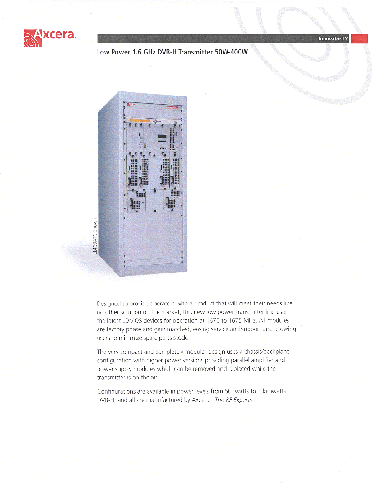
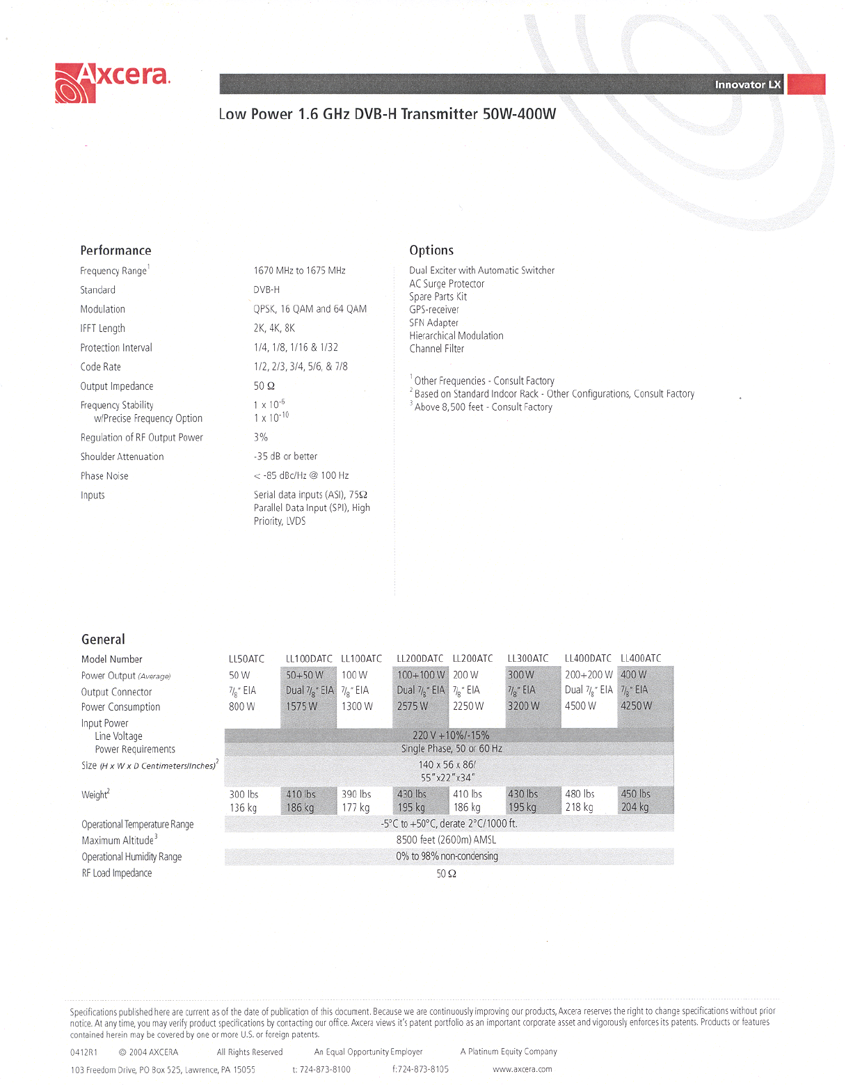
APPENDIX B
DRAWINGS AND PARTS LISTS

1.67 GHz 50 Watt Single Output Transmitter Appendix B, Drawings and Parts Lists
LL50ATC, Rev. 0 B-1
Innovator LX Series 1.67 GHz Digital Transmitter System
Chassis Assembly, 220 VAC Exciter, 1.67 GHz
Interconnect.................................................................................1305023
Backplane Board, 1.67 GHz
Schematic ....................................................................................1304893
Metering Assembly, 1.67 GHz
Interconnect Drawing .....................................................................1304975
Metering Board, 1.67 GHz
Schematic ....................................................................................1304923
Upconverter Assembly, Single Output, 1.67 GHz
Interconnect.................................................................................1305063
Upconverter Control Board, 1.67 GHz
Schematic ....................................................................................1304781
Upconverter Board, 1.67 GHz
Schematic ....................................................................................1304930
L.O. Generator Board, Single Output, 1.67 GHz
Schematic ....................................................................................1304941
Control/Power Supply Assembly, 220 VAC, 1.67 GHz
Interconnect.................................................................................1305037
Switch Board
Schematic .................................................................................1527-3406
Control Board
Schematic ....................................................................................1302023
Power Protection Board
Schematic ....................................................................................1302839
5 Watt Driver Power Amplifier Assembly, 1.67 GHz
Interconnect.................................................................................1305055
Amplifier Module Control Board, 1.67 GHz
Schematic ....................................................................................1304776
Two Stage 40W Amplifier Module, 1.67 GHz
Schematic ....................................................................................1304866

1.67 GHz 50 Watt Single Output Transmitter Appendix B, Drawings and Parts Lists
LL50ATC, Rev. 0 B-2
Chassis Assembly, Power Amplifier, LL200ATC
LL100ATC AC Harness Chassis/Airbox Interconnect...............................1305882
LL100ATC DC Harness, Chassis/Airbox Interconnect..............................1305885
LL100ATC Coax Assembly Chassis/Airbox Interconnect..........................1305883
External Amplifier Signal Board
Schematic ....................................................................................1303346
Power Amplifier Assembly, 100 Watt, 1.67 GHz
(One Power Amplifier Assembly is used in a LL100ATC)
Interconnect.................................................................................1305145
Quad Stage Pallet
Schematic ....................................................................................1304608
Single Stage Pallet, V2, 1.67 GHz
Schematic ....................................................................................1304546
Amplifier Module Control Board, 1.67 GHz
Schematic ....................................................................................1304776
Phase/Gain Board, 1.67 GHz
Schematic ....................................................................................1305027
Power Supply Assembly, 2 kW, 1.67 GHz
(The Power Supply Assembly Supplies Power to the Two
Power Amplifier Assemblies)
Block Diagram................................................................................1303886
Interconnect.................................................................................1303479