UTStarcom Korea Technologies CDMRF102 Dual-Band CDMA Module (CDMA/PCS CDMA) User Manual CDMRF102 user manual
UTStarcom Korea Technologies Ltd. Dual-Band CDMA Module (CDMA/PCS CDMA) CDMRF102 user manual
UserManual.wiki
>
UTStarcom Korea Technologies
>
CDMRF102 User Manual
Users Manual
Navigation menu
Upload a User Manual
Namespaces
Wiki Guide
HTML
PDF
Info
Views
User Manual
Discussion / Help
Navigation
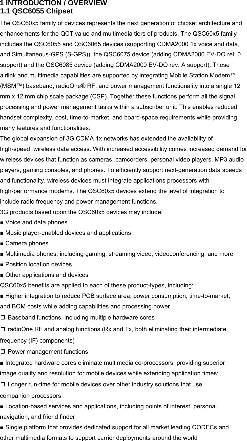
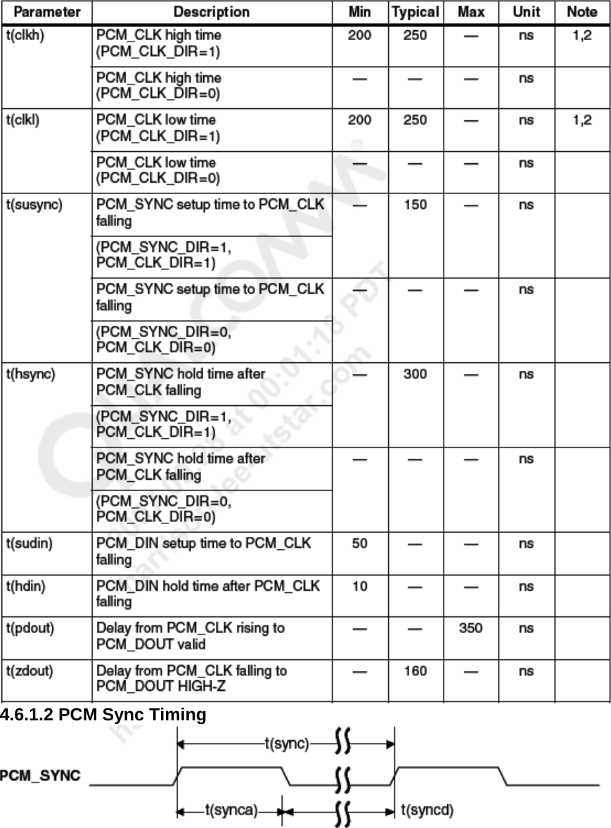
![4.3.2 Standby Current Drain. Band Celluar (ch 384) PCS (ch 600) Slot Mode SLOT1 SLOT2 SLOT1 SLOT2 Current [mA] 3.78 mA 2.63 mA 3.76 mA 2.59 mA 4.3.3 Off current drain. -Under 100uA 4.4 Output Power The phone output power is measured at the end of phone module antenna connector using the RF power meter. The power level of the phone module is controlled by the base station and the range of the power level is varied from Min output power to Max output power that is defined in the table below. Item Specification Min Typical Maximum UnitMax Output Power Power Class II 23 24 26 dBm/1.23MHzMin Output Power -53 -50 dBm/1.23MHz 4.6 Audio Interface 4.6.1 PCM Audio 4.6.1.1 QSC Timing Parameters](https://usermanual.wiki/UTStarcom-Korea-Technologies/CDMRF102/User-Guide-999714-Page-13.png)