UTStarcom Korea Technologies CDMRF102 Dual-Band CDMA Module (CDMA/PCS CDMA) User Manual CDMRF102 user manual
UTStarcom Korea Technologies Ltd. Dual-Band CDMA Module (CDMA/PCS CDMA) CDMRF102 user manual
Users Manual

CDMRF102
TCU Phone Module
Component Technical Specification Manual
Ver. 0.1
Aug. 14. 2008
Table of Contents
CDMRF102..................................................................................................................................................... 1
TCU PHONE MODULE.................................................................................................................................. 1
1 INTRODUCTION / OVERVIEW .................................................................................................................. 6
1.1 QSC 6055 Chipset .............................................................................................................................. 6
1.1.1 QSC 6055 Features........................................................................................................................... 6
1.2 IS- Mobile Standards .......................................................................................................................... 7
1.3 Acronym Definitions........................................................................................................................... 8
1.4 Development Tools for the Phone Module....................................................................................... 8
1.4.1 LT Box...................................................................................................................................... ...……8
2 MECHANICAL DESCRIPTION .................................................................................................................. 9
2.1 Phone Module Mechanical Outline ................................................................................................... 9
2.2 Phone Module I/O Connector ............................................................................................................ 9
2.2.1 I/O Connector Drawing and Supplier Part Number…......................................................................... 9
2.2.2 I/O Connector Electrical Characteristics ….......................................................................................10
2.2.2.1 I/O Connector Pin Assignment ..................................................................................................... 10
3 OPERATING TEMPERATURE AND STORAGE ..................................................................................... 13
3.1 Temperature ...................................................................................................................................... 13
3.1.1 Storage Temperature….................................................................................................................... 13
3.1.2 Operating Temperature…................................................................................................................ 13
4 ELECTRICAL INTERFACE...................................................................................................................... 14
4.1 Design Guidelines ............................................................................................................................ 14
4.1.1 Component Derating…..................................................................................................................... 14
4.1.1.1 Ceramic Capacitors / Parallel Plate Capacitors……….................................................................. 14
4.1.1.2 Electrolytic Capacitors .................................................................................................................. 14
4.1.1.3 Tantalum Capacitors..................................................................................................................... 14
4.1.2 Communication Pins and Unused Pins............................................................................................ 14
4.2 Supply Voltage................................................................................................................................... 14
4.3 Current Draw ....................................................................................................................................... 15
4.4 Output Power ...................................................................................................................................... 16
4.5 Audio Interface.................................................................................................................................... 16
4.5.1 PCM Audio....................................................................................................................................…..16
4.5.1.1 QSC Timing Parameters ..............................................................................................................…16
4.5.1.2 PCM Sync Timing ........................................................................................................................... 16
4.5.1.3 QSC Receive Timing........................................................................................................................17
4.5.1.4 QSC Transmitting Timing................................................................................................................ 17
4.5.2 UART Data Interface.......................................................................................................................... 17
4.5.3 Cellular Antenna Open/Short Sense................................................................................................ ..19
1 INTRODUCTION / OVERVIEW
1.1 QSC6055 Chipset
The QSC60x5 family of devices represents the next generation of chipset architecture and
enhancements for the QCT value and multimedia tiers of products. The QSC60x5 family
includes the QSC6055 and QSC6065 devices (supporting CDMA2000 1x voice and data,
and Simultaneous-GPS (S-GPS)), the QSC6075 device (adding CDMA2000 EV-DO rel. 0
support) and the QSC6085 device (adding CDMA2000 EV-DO rev. A support). These
airlink and multimedia capabilities are supported by integrating Mobile Station Modem™
(MSM™) baseband, radioOne® RF, and power management functionality into a single 12
mm x 12 mm chip scale package (CSP). Together these functions perform all the signal
processing and power management tasks within a subscriber unit. This enables reduced
handset complexity, cost, time-to-market, and board-space requirements while providing
many features and functionalities.
The global expansion of 3G CDMA 1x networks has extended the availability of
high-speed, wireless data access. With increased accessibility comes increased demand for
wireless devices that function as cameras, camcorders, personal video players, MP3 audio
players, gaming consoles, and phones. To efficiently support next-generation data speeds
and functionality, wireless devices must integrate applications processors with
high-performance modems. The QSC60x5 devices extend the level of integration to
include radio frequency and power management functions.
3G products based upon the QSC60x5 devices may include:
■ Voice and data phones
■ Music player-enabled devices and applications
■ Camera phones
■ Multimedia phones, including gaming, streaming video, videoconferencing, and more
■ Position location devices
■ Other applications and devices
QSC60x5 benefits are applied to each of these product-types, including:
■ Higher integration to reduce PCB surface area, power consumption, time-to-market,
and BOM costs while adding capabilities and processing power
❒ Baseband functions, including multiple hardware cores
❒ radioOne RF and analog functions (Rx and Tx, both eliminating their intermediate
frequency (IF) components)
❒ Power management functions
■ Integrated hardware cores eliminate multimedia co-processors, providing superior
image quality and resolution for mobile devices while extending application times:
❒ Longer run-time for mobile devices over other industry solutions that use
companion processors
■ Location-based services and applications, including points of interest, personal
navigation, and friend finder
■ Single platform that provides dedicated support for all market leading CODECs and
other multimedia formats to support carrier deployments around the world
■ DC power reduction using innovative techniques, such as the QUALCOMM
IntelliCeiver™ technology and PA bypassing
1.1.1 QSC6055 Features
■ Modem microprocessor – a low-power, high-performance RISC microprocessor core
running at 192 MHz and featuring the ARM926EJ-S™ CPU and Jazelle™ accelerator
circuit from ARM® Limited.
■ Modem digital signal processor (mDSP) – the low-power, high-performance
QDSP4u8™ targeting 85 MHz.
■ Application digital signal processor (aDSP) – the low-power, high-performance
QDSP4u8™ targeting 115 MHz.
■ 96 MHz bus clock for 16-bit DDR SDRAM and 16/32-bit PSRAM
■ Dual-memory buses separating the high-speed memory subsystem (EBI1) from
low-speed peripherals (EBI2), such as LCD panels
■ 1.8 V memory interface support on EBI1
■ 1.8 V or 2.6 V memory interface support on EBI2
■ Memory types supported:
❒ 16-bit NOR flash (burst mode), including multiplexed address/data types
❒ 8-bit and 16-bit NAND flash and 16-bit OneNAND
❒ 16-bit DDR SDRAM
❒ 16-bit and 32-bit PSRAM requiring multiplexed address/data types
■ Bootup is supported from the following devices:
❒ Burst NOR on EBI1
❒ Any supported NAND memory type on EBI2
■ CDMA2000 1X revisions A and B
■ Enhanced GPS position location
❒ Integrated gpsOne functionality, featuring enhancements by SnapTrack®, Inc., to
enable a wide variety of location-based services and applications, including points
of interest, personal navigation, and friend finder
❒ Simultaneous-GPS (processes GPS on its Rx path while CDMA signals continue
to be processed on a separate Rx path)
❒ 1024x searcher, DFT accelerator, off-chip RAM for measured data storage
■ Two universal asynchronous receiver transmitter (UART) serial ports
1.2 Mobile Standards
Service Provisioning- OTASP ANSI TIA EIA-683
Parameter Administration - OTAPA ANSI TTA ETA-683
Caller ID IS-2000
Call Hold & Call Waiting IS-2000
Three-Way Calling IS-41
E911 Location Determination TIA EIA IS-801
CDMA 1xRTT Packet Data (153 Kbps forward
and reverse)
TIA EIA IS-2000
Mobile IP TIA EIA IS-835-A
Enhanced Variable Rate Codec-B (EVRC-B) 3GPP2 C.S0014.B
Enhanced Variable Rate Codec (EVRC) TIA EIA IS-127
EVRC TTY TDD Extension TTA ETA IS-127-3
SMS (MT,MO) IS-637
1.3 Acronym Definitions
Define all acronyms that will be used in the document
1.4 Development Tools for the Phone Module
1.4.1 LT Box
2 MECHANICAL DESCRIPTION
2.1 Phone Module Mechanical Outline
2.2 Phone Module I/O Connector
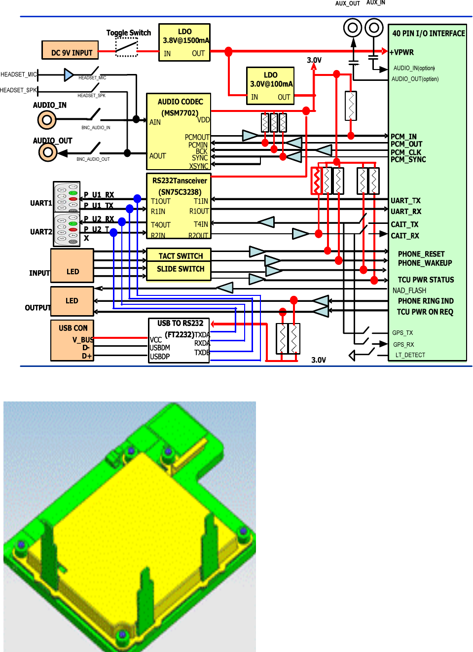
Iriso Part Number: 9827B-40BGFC (connector only) 9827B-40Y912 (tape and reel)

2.2.1 I/O Connector Drawing and Supplier Part Number
This connector is placed on the phone module
2.2.2 I/O Connector Electrical Characteristics
I
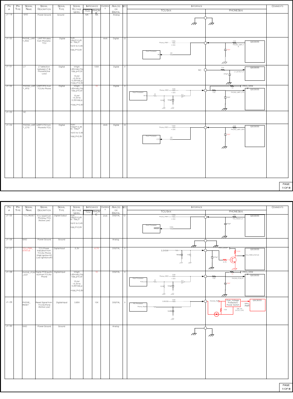
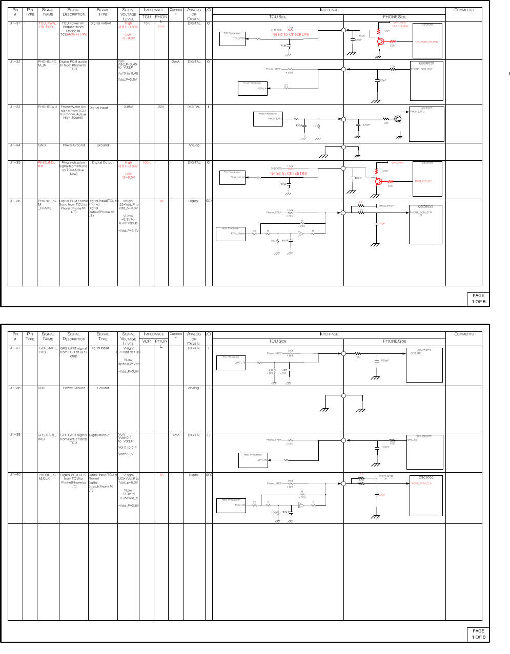
2.2.2.1 I/O Connector Pin Assignment, I/O Interface, and Circuit Diagrams
Phone_PWR Min:
3.61V
Max:
3.99V
Max:
1.5A
I
SIGNAL
DESCRIPTION
SIGNAL
VOLTAGE
LEVEL
IMPEDANCE
TCU PHON
E
CURREN
T
I/O INTERFACE
TCU SIDE PHONE SIDE
SIGNAL
NAME
COMMENTSSIGNAL
TYPE
ANALOG
OR
DIGITAL
DC input. ANALOG
PIN
#
J1-1
PIN
TYPE
J1-2
J1-3
J1-4
J1-5
J1-6
Phone_PWR
Phone_PWR
Phone_PWR
GND
GND
3.8 volts supply
voltage to phone
module
3.8 volts supply
voltage to phone
module
DC input. Min:
3.61V
Max:
3.99V
NA NA
NANA Max:
1.5A
ANALOG I
3.8 volts supply
voltage to phone
module
DC input. Min:
3.61V
Max:
3.99V
NA NA Max:
1.5A
ANALOG I
3.8 volts supply
voltage to phone
module
DC input. Min:
3.61V
Max:
3.99V
NA NA Max:
1.5A
ANALOG I
Over_Voltage
Protection
3.8V QSC6055
VPH_
PWR
4.7
uf
1000pf0.01 f1000pf200 f
3.85V
Switching
Reg
LTC3835
22 H
40m
10
10
15
15
FBATT
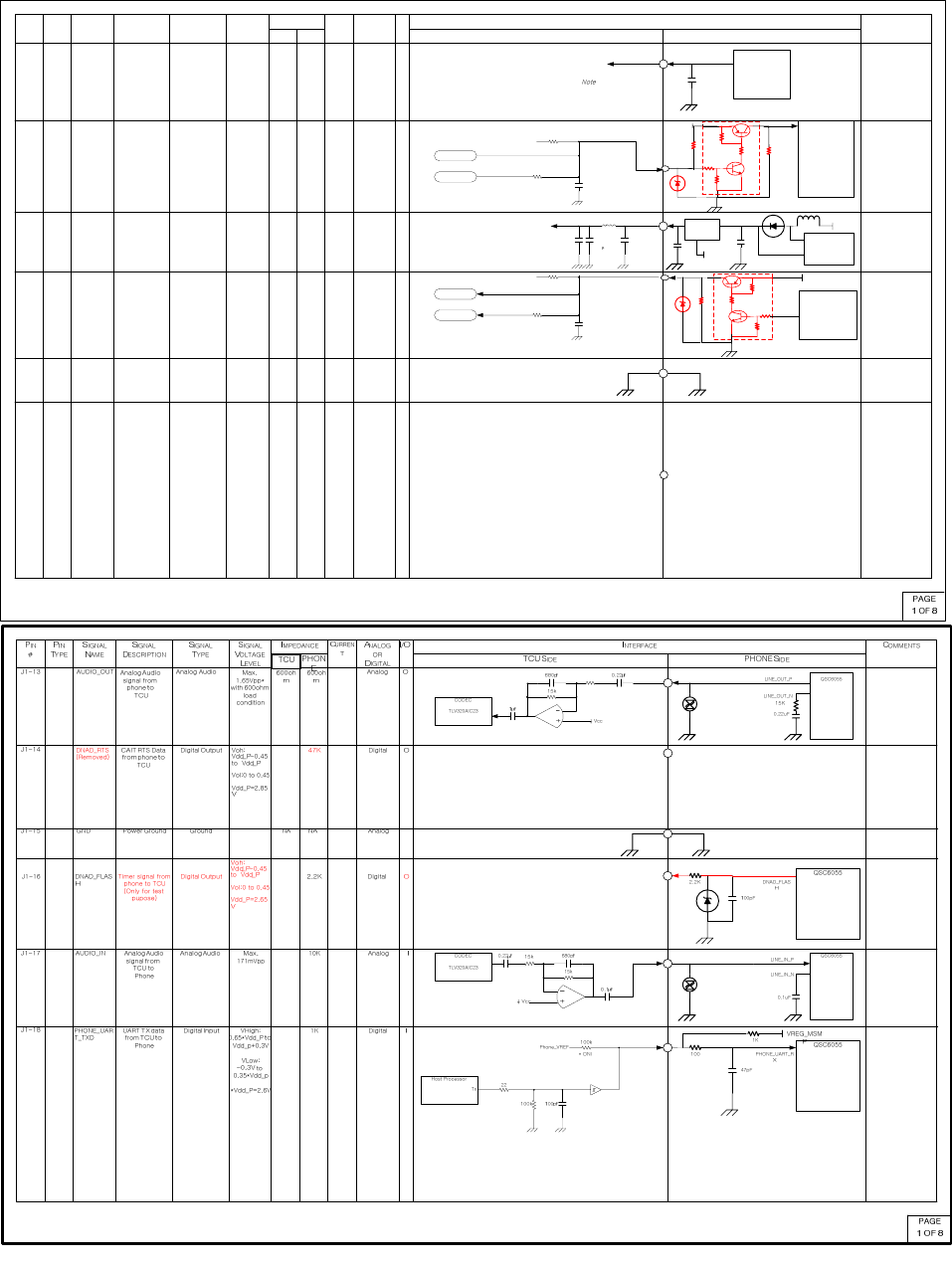
SIGNAL
DESCRIPTION
SIGNAL
VOLTAGE
LEVEL
IMPEDANCE
PHON
E
CURREN
T
I/O INTERFACE
TCU SIDE PHONE SIDE
SIGNAL
NAME
Phone_VRE
F
O
SIGNAL
TYPE
ANALOG
OR
DIGITAL
COMMENTS
DC supply output Analog
PIN
#
PIN
TYPE
J1-7
J1-8
J1-9
J1-10
J1-11
J1-12
DNAD_RX
5VSW_FRO
M_PHONE
DNAD_TX
GND
DNAD_CTS
(Removed)
2.6V +/- 2%
supply output from
NAD to TCU
Min.:2.548V.
Max:2.652V
NA NA
CAIT Receive Data
from TCU to
Phone.
Digital input VHigh:
0.65*Vdd_P to
Vdd_p+0.3V
VLow:
-0.3V to
0.35*Vdd_p
*Vdd_P=2.85V
10K
10mA
Digital I
5V +/- 5%
supply output from
NAD to TCU
DC supply output Min.:4.75V.
Max:5.25V NA NA 70mA Analog O
CAIT transmit
Data
from phone to
TCU
Digital Output Voh:
Vdd_P-0.45
to Vdd_P
Vol:0 to 0.45
Vdd_P=2.85
V
47K Digital O
Power Ground Ground NA NA Analog
CAIT CTS data
from TCU from
Phone
Digital Input VHigh:
0.65*Vdd_P to
Vdd_p+0.3V
VLow:
-0.3V to
0.35*Vdd_p
*Vdd_P=2.85V
10K Digital I
TCU
2.2uF
QSC6055
VREG_MSMP
2.6v
VPH_PW
R
QSC6055
VSW_5V
VREG_5
V
10u
F
Current Limit
Switch(200mA)
5VSW_PWR_E
N
1000pF
2.2uH
2.6V
V4 – A4
V3 – B9
* DNI 1000pF
* DNI
0
: Phone_VREF
is routed to pullups
on RESET, UART,
PCM, lines
0.01 f1000pf1000pf
5V
Phone_VREF 100k
* DNI
V4 – A5
V3 – B10
* DNI 1000pF
* DNI
0
Phone_VREF 100k
* DNI
VREG_2.85V
QSC6055
CAIT_RX
4.7K
c
QSC6055
CAIT_TX
VREG_2.85V
4.7K
2.2K(DNI)
3 OPERATING TEMPERATURE AND STORAGE
3.1 Temperature
3.1.1 Storage Temperature
The phone module shall be capable of being stored at -40C ~ 85C without any damage.
3.1.2 Operating Temperature
The phone module shall operate within specification from -30C – 85C
4 ELECTRICAL INTERFACE
Phone / TCU System Mechanization
4.1 Design Guidelines
4.1.1 Component Derating
4.1.1.1 Ceramic Capacitors / Parallel Plate Capacitors
Ceramic capacitors or parallel plate capacitors on power lines shall be two devices in
series to protect against capacitor shorts.
4.1.1.2 Electrolytic Capacitors
Electrolytic capacitors shall be rated at 2x the maximum voltage for a given circuit.
4.1.1.3 Tantalum Capacitors
Tantalum capacitors shall be rated at 3x the maximum voltage for a given circuit on a
power supply. They shall be rated at 2X for applications on signal lines.
Tantalum capacitors shall not be placed on circuits with currents that exceed a current of
1A or the current shall be limited to 1A.
4.1.2 Communication Pins and Unused Pins
Serial communications signals shall be terminated per manufacturers specifications.
Unused IC pins should be terminated according to manufacturer’s recommendations.
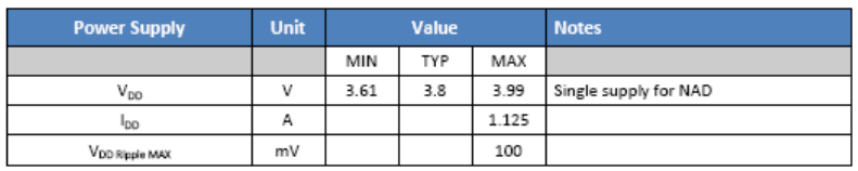
4.2 Supply Voltage
A power supply or supplies with the following characteristics shall power the NAD:
Note: Phone Module should not be damaged by the instantaneous loss of the supply
voltage
4.3 Current Draw
4.3.1 TX Current Drain
<Voice Call>
-. USCellular(Ch.384) Current: 245 mA
-. USPCS(Ch.675) Current : 230 mA
<Data Call>
-. USCellular(Ch.384) Current: 350 mA
-. USPCS(Ch.675) Current: 360 mA
4.3.2 Standby Current Drain.
Band Celluar (ch 384) PCS (ch 600)
Slot Mode SLOT1 SLOT2 SLOT1 SLOT2
Current [mA] 3.78 mA 2.63 mA 3.76 mA 2.59 mA
4.3.3 Off current drain.
-Under 100uA
4.4 Output Power
The phone output power is measured at the end of phone module antenna connector using
the RF power meter. The power level of the phone module is controlled by the base station
and the range of the power level is varied from Min output power to Max output power that is
defined in the table below.
Item Specification Min Typical Maximum Unit
Max Output Power Power Class II 23 24 26 dBm/1.23MHz
Min Output Power -53 -50 dBm/1.23MHz
4.6 Audio Interface
4.6.1 PCM Audio
4.6.1.1 QSC Timing Parameters
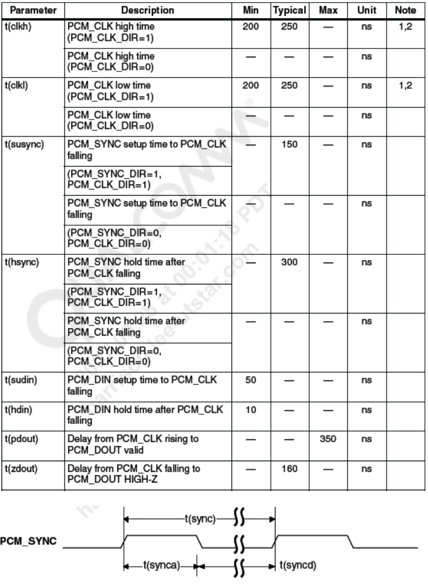
4.6.1.2 PCM Sync Timing
4.6.1.3 QSC Receive Timing
4.6.1.4 MSM Transmitting Timing
4.6.2 UART Data Interface
QSC6055 devices are capable of providing up to two universal asynchronous receiver
transmitter (UART) ports. Each UART communicates with serial data ports that conform
to the RS-232 interface protocol. With a properly written and user-defined download
program, the UART can be used as the handset’s serial data port for test and debug, and
can support additional interface functions such as an external keypad or ringer. If the
handset uses EEPROM or flash memory, then the UART can be used to load and/or
upgrade system software.
UART1 capability is expanded to include a high-speed (Up to 4 Mbps) mode.
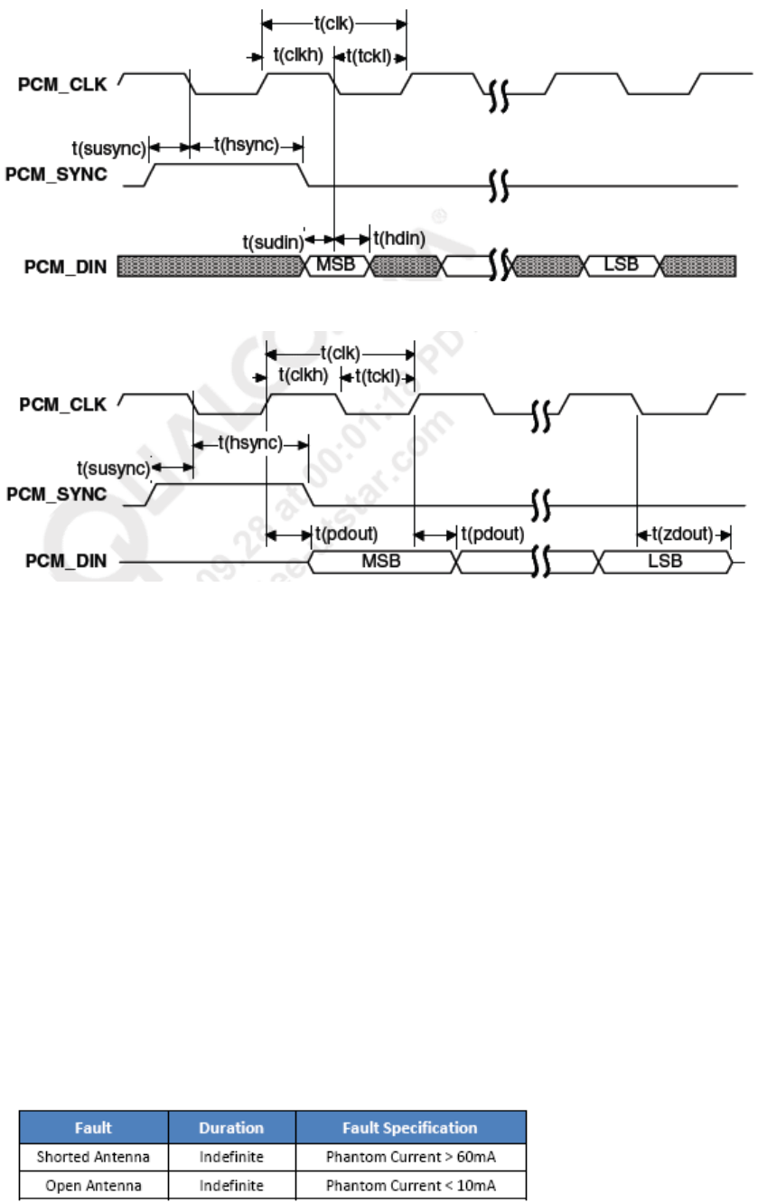
4.6.3 Cellular Antenna Open/Short Sense
The phone module provides the antenna diagnostics function by the antenna detection cir-
cuit. The antenna detection circuit can detect three statuses: GOOD, OPEN and
SHORTED. The detection circuit senses current drain through anttena and sends analog
voltage to QSC. QSC reads analog voltage by its ADC and monitors the antenna status.
<Antenna Input Fault Requirement>
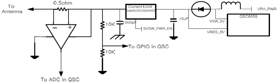
<Antenna Detection Circuit>

Notice
OEM integrators and installers are instructed that the phrase. This device contains
transmitter FCC ID: O6Y-CDMRF102 must be placed on the outside of the host.
Warning: Exposure to Radio Frequency Radiation The radiated output
power of this device is far below the FCC radio frequency exposure
limits. Nevertheless, the device should be used in such a manner that
the potential for human contact during normal operation is minimized.
In order to avoid the possibility of exceeding the FCC radio
frequency exposure limits, human proximity to the antenna should
not be less than 20cm during normal operation. The gain of the
antenna for Cellular band must not exceed-1.5 dBi.
The gain of the antenna for PCS band must not exceed -2.5dBi.