Unigen UGWANBL2 Bluetooth Low Energy Module User Manual
Unigen Corporation Bluetooth Low Energy Module
Unigen >
user manual
Solutions for a Real Time World ANTHIAS BLE Module
User Manual
Re-Tek - xxxx - 1 - 45388 Warm Springs Blvd. Fremont, CA 94539
support@unigen.com TEL: (510) 668.2088 FAX: (510) 661.2788
http://www.unigen.com Customer Comment Line: (800) 826.0808
Copyright Unigen Corporation, 2012
Unigen Corp. Wireless Module Products
ANTHIAS Single Mode Bluetooth Low Energy Radio Module
UGWANBL2SME133A
UGWANBL2SME133U
Issue Date: 22-Feb-12
Revision: 1.1
Solutions for a Real Time World ANTHIAS BLE Module
User Manual
Re-Tek - xxxx - 2 - 45388 Warm Springs Blvd. Fremont, CA 94539
support@unigen.com TEL: (510) 668.2088 FAX: (510) 661.2788
http://www.unigen.com Customer Comment Line: (800) 826.0808
Copyright Unigen Corporation, 2012
Revision History
Rev. No. History Issue Date Remarks
1.1 Preliminary
Release Feb. 22, 2012 Advanced information; Author: Allen B. Cabreros
This document is provided “as is” with no warranties whatsoever, including any warranty of
merchantability, non-infringement, fitness for any particular purpose, or any warranty otherwise
arising out of any proposal, specification or sample.
Unigen Corporation disclaims all liability, including liability for infringement of any proprietary
rights, relating to use of information in this document. No license, expressed or implied, by
estoppel or otherwise, to any intellectual property rights is granted herein.
*Third-party brands, names, and trademarks are the property of their respective owners.

Solutions for a Real Time World ANTHIAS BLE Module
User Manual
Re-Tek - xxxx - 3 - 45388 Warm Springs Blvd. Fremont, CA 94539
support@unigen.com TEL: (510) 668.2088 FAX: (510) 661.2788
http://www.unigen.com Customer Comment Line: (800) 826.0808
Copyright Unigen Corporation, 2012
TABLE OF CONTENTS
LIST OF FIGURES __________________________________________ 4
LIST OF TABLES ___________________________________________ 4
PRODUCT INTRODUCTION ___________________________________ 5
FEATURES AND BENEFITS ____________________________________ 5
APPLICATIONS ____________________________________________ 6
PRODUCT DESCRIPTION _____________________________________ 7
MODULE DETAILS __________________________________________ 7
FUNCTIONAL OVERVIEW ____________________________________ 8
MODULE PAD ASSIGNMENT __________________________________ 10
DEVICE TERMINAL FUNCTIONS _______________________________ 11
ELECTRICAL CHARACTERISTICS _______________________________ 12
Absolute Maximum Ratings ________________________________ 12
Recommended Operating Conditions ________________________ 12
Input/Output Terminal Characteristics _______________________ 13
ESD PROTECTION __________________________________________ 14
RF CHARACTERISTICS ______________________________________ 14
AGENCY CERTIFICATIONS ___________________________________ 15
BLUETOOTH COMPLIANCE ___________________________________ 15
TBDBLUETOOTH SOFTWARE STACK ____________________________ 15
BLUETOOTH SOFTWARE STACK _______________________________ 16
SOFTWARE DEVELOPMENT ___________________________________ 17
MICROCONTROLLER, MEMORY, IO AND BASEBAND LOGIC __________ 18
System Ram ___________________________________________ 18
Internal ROM ___________________________________________ 18
Microcontroller _________________________________________ 19
Programmable I/O Ports, PIO and AIO _______________________ 19
LED Flasher / PWM modules _______________________________ 20
POWER CONTROL, REGULATION AND RESET _____________________ 20
Internal Switch-mode Regulator ____________________________ 20
Internal Low-voltage Linear Regulator _______________________ 20
Reset _________________________________________________ 21
Digital Pad States on Reset ________________________________ 21
SERIAL INTERFACES ________________________________________ 21
Application UART Interface ________________________________ 21
SPI Master Serial Flash Interface ___________________________ 22
Programming and Debug Interface __________________________ 23
POWER CONSUMPTION _____________________________________ 25
EXAMPLE SCHEMATICS ______________________________________ 27
No Serial Flash _________________________________________ 27
External Serial Flash Configuration __________________________ 28
MECHANICAL DRAWINGS ____________________________________ 29

Solutions for a Real Time World ANTHIAS BLE Module
User Manual
Re-Tek - xxxx - 4 - 45388 Warm Springs Blvd. Fremont, CA 94539
support@unigen.com TEL: (510) 668.2088 FAX: (510) 661.2788
http://www.unigen.com Customer Comment Line: (800) 826.0808
Copyright Unigen Corporation, 2012
Dimensions ____________________________________________ 29
LGA Pads and Landing Pattern _____________________________ 30
ORDERING INFORMATION ___________________________________ 31
CONTACT INFORMATION ____________________________________ 31
LIST OF FIGURES
Figure 1: Anthias Module Block Diagram ________________________ Error!
Bookmark not defined.
Figure 2: Anthias Pad Location (Top View) _______________________ 10
Figure 3: Anthias Bluetooth 4.0 Firmware Stack ___________________ 16
Figure 4: Microcontroller, Memory, IO, Baseband Logic Diagram ______ 18
Figure 5: Anthias Internal Regulation Block ______________________ 20
Figure 6: External Serial EEPROM Circuitry _______________________ 22
Figure 7: Idle Connection State _______________________________ 26
Figure 8: Embedded EEPROM Example Schematic _________________ 27
Figure 10: External Serial Flash Example Schematic _______________ 28
Figure 11: ANTHIAS Mechanical Drawing ________________________ 29
Figure 12: Landing Pattern ___________________________________ 30
LIST OF TABLES
TABLE 1: DEVICE TERMINAL FUNCTIONS ________________________ 11
TABLE 2: ABSOLUTE MAXIMUM RATINGS ________________________ 12
TABLE 3: RECOMMENDED OPERATING CONDITIONS _______________ 12
TABLE 4: DIGITAL TERMINAL CHARACTERISTICS _________________ 13
TABLE 5: ANALOG TERMINAL CHARACTERISTICS _________________ 13
TABLE 6: ESD RATINGS ______________________________________ 14
TABLE 7: RF CHARACTERISTICS _______________________________ 14
TABLE 8: WAKE OPTIONS ____________________________________ 19
TABLE 9: DIGITAL PAD STATE ON RESET ________________________ 21
TABLE 10: ANTHIAS UART PARAMETERS ________________________ 22
TABLE 11: ANTHIAS EXTERNAL SERIAL FLASH SIGNALS ____________ 23
TABLE 12: SPI TRANSACTIONS ________________________________ 24
TABLE 13: OPERATING POWER CONSUMPTION FIGURES ___________ 25
TABLE 14: PART NUMBERS ___________________________________ 31

Solutions for a Real Time World ANTHIAS BLE Module
User Manual
Re-Tek - xxxx - 5 - 45388 Warm Springs Blvd. Fremont, CA 94539
support@unigen.com TEL: (510) 668.2088 FAX: (510) 661.2788
http://www.unigen.com Customer Comment Line: (800) 826.0808
Copyright Unigen Corporation, 2012
PRODUCT INTRODUCTION
Anthias is a product from the Unigen BTLE family. Anthias is a single-mode Bluetooth Low Energy
(BLE) module solution. Anthias enables ultra low-power connectivity data transfer for applications
previously limited by the power consumption, size constraints and complexity of other wireless
standards. The Anthias module provides everything required to create a Bluetooth low energy
product with RF, baseband, microcontroller, qualified Bluetooth v4.0 stack and customer
application running on a single module.
FEATURES AND BENEFITS
Bluetooth Low Energy v4.0
Chip antenna or U.FL RF connector configuration
512K programmable EEPROM for BLE profiles and applications
Optional external Serial Flash support
64K of RAM
32KHz clock included with watchdog timer for ultra low power dormant modes
Accessible UART interface to embedded applications
12 Digital I/O pads
3 AIO pads; 10-bit ADC
2 LED pads supporting Pulse Width Modulation (PWM)
~ +7dBm transmit output power
~ -89dBm receiver sensitivity
RSSI monitoring for proximity applications
Size: 22 x 18 x 3 (mm)
25 pad LGA Surface Mount form factor
-20C to +70C temperature range
Power Consumption: 16mA Peak; < 600nA dormant mode
Certifications: TDB

Solutions for a Real Time World ANTHIAS BLE Module
User Manual
Re-Tek - xxxx - 6 - 45388 Warm Springs Blvd. Fremont, CA 94539
support@unigen.com TEL: (510) 668.2088 FAX: (510) 661.2788
http://www.unigen.com Customer Comment Line: (800) 826.0808
Copyright Unigen Corporation, 2012
APPLICATIONS
The Anthias module is an important block in building an ecosystem using Bluetooth Low Energy.
Bluetooth Low Energy enables the transfer of simple data sets between compact devices opening
up a completely new class of Bluetooth applications such as watches, TV remote controls, medical
sensors and fitness trainers. Bluetooth Low Energy takes less time to make a connection than
conventional Bluetooth wireless technology and can consume approximately 1/20th of the power
of Bluetooth Basic Rate. Anthias supports profiles for sensors, watches, HIDs and time
synchronization.
Security & Proximity
Key Tags/FOBS
Proximity Sensors/Monitoring
Medical, Health, Sport & Fitness
Blood Pressure Monitors
Wearable Heart Rate Monitors
Weight Scales
Pedometers
Medical Sensors
Medical Telemetry
Glucose Meters
Emergency Callers
Medical Identification/Asset Tracking
Medical Equipment Control
Fitness Machines
Speed Sensors
Human Interface Devices & Industrial Control
Remote Control
Mouse
Game Controller
Industrial Control & Smart Energy
Remote On/Off Switch
Thermostats
Smart Appliances
Kiosks
Smart Bar Code Scanner/Readers

Solutions for a Real Time World ANTHIAS BLE Module
User Manual
Re-Tek - xxxx - 7 - 45388 Warm Springs Blvd. Fremont, CA 94539
support@unigen.com TEL: (510) 668.2088 FAX: (510) 661.2788
http://www.unigen.com Customer Comment Line: (800) 826.0808
Copyright Unigen Corporation, 2012
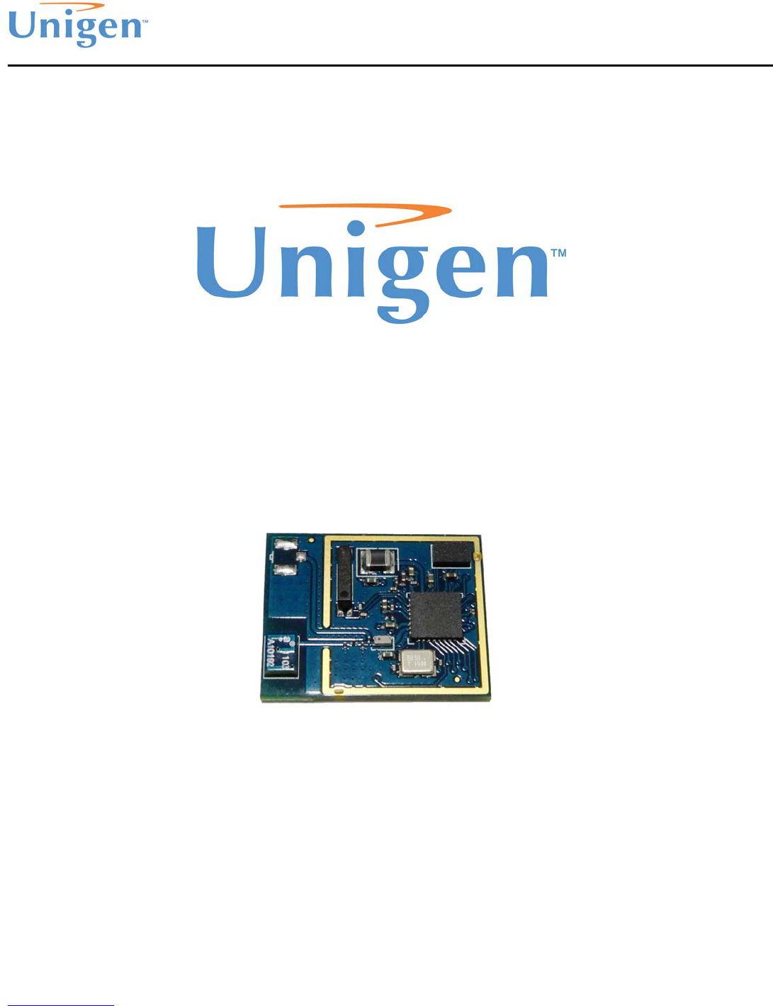
PRODUCT DESCRIPTION
The Anthias module is a complete Bluetooth Low Energy module solution. Anthias includes the
Bluetooth Low Energy radio transceiver, 32 kHz slow clock for ultra low power modes, internal
microcontroller for BLE applications software and profiles. Anthias is based on Cambridge Silicon
Radios CSR1000™ chipset. The module is capable of supporting embedded applications along
with ATT, GATT, SMP, L2CAP and GAP BLE stack component. The module is a separate PCB with
contained RF design in a 22mm x 18mm x 3mm compact design. The RF output can be either
through an on-board chip antenna or taken to an external antenna via a U.FL mini-coaxial
connector.
MODULE DETAILS
Bluetooth Low Energy Radio
+7dBm with power level control from
integrated 6-bit DAC over a dynamic range
>30dB.
-89dBm receiver sensitivity with integrated
channel filters, digital demodulator for improved
sensitivity and co-channel rejection and fast AGC
for enhanced dynamic range.
Baseband and Software
Hardware MAC for all packet types enables
packet handling without involving the MCU.
Auxiliary Features
Power management features with software
shutdown and hardware wake-up
Internal 32KHz clock for dormant modes
Power-on-reset cell detects low supply voltage
Physical Interfaces
SPI master interface
SPI Programming and debug interface
I²C
Digital PIOs
Analog IOs
Bluetooth Stack
Bluetooth v4.0 specification protocol
stack runs on integrated MCU.
Slave operation (master operation
possible later with firmware update)
Includes Encryption
GAP profile
L2CAP
Security Manager
Attribute Protocol and Profile
Bluetooth Low Energy profile support
Package
Size: 22 x 18 x 3 (mm)
25 pad LGA Surface Mount

Solutions for a Real Time World ANTHIAS BLE Module
User Manual
Re-Tek - xxxx - 8 - 45388 Warm Springs Blvd. Fremont, CA 94539
support@unigen.com TEL: (510) 668.2088 FAX: (510) 661.2788
http://www.unigen.com Customer Comment Line: (800) 826.0808
Copyright Unigen Corporation, 2012
FUNCTIONAL OVERVIEW
The Anthias is a complete Radio Transceiver Module with operating in the license free ISM
(Industrial Scientific and Medical) 2.4GHz band. Anthias is equipped with a crystal oscillator, band
pass filter, EEPROM for application code and chip antenna. Anthias incorporates Cambridge Silicon
Radio’s CSR1000™ chipset that is fully compliant to the Bluetooth v4.0 specifications.
The module has a RISC microcontroller that embeds the Bluetooth v4.0 stack and is able to run
application code to become a complete embedded stand alone solution. 64KB of integrated RAM
supports the RISC microcontroller and is shared between the ring buffers which are used to hold
data for each active connection and the general-purpose memory required by the Bluetooth stack.
The microcontroller interrupt controller and event timer executes the Bluetooth software stack,
control the BLE radio and external interfaces. A 16-bit RISC microcontroller is used for low power
consumption and efficient use of memory.

Solutions for a Real Time World ANTHIAS BLE Module
User Manual
Re-Tek - xxxx - 9 - 45388 Warm Springs Blvd. Fremont, CA 94539
support@unigen.com TEL: (510) 668.2088 FAX: (510) 661.2788
http://www.unigen.com Customer Comment Line: (800) 826.0808
Copyright Unigen Corporation, 2012
Anthias also supports programmable I/O ports, PIO and AIO. These ports can be accessed by the
RISC microcontroller and application code. A SPI interface is used for programming and
debugging of develop application code executed on the module. A UART interface is also available
that is shared with the PIO pads. An external I²C/Serial Flash interface is an available
configuration option for products to utilize an external serial flash and have a lower cost module.
The Anthias RF output can either be through an on-board chip antenna or it can be routed to an
external antenna through a mini-coaxial U.FL RF connector. The RF out is matched to 50 Ohms.
An RF shield is provided to prevent RF coupling back into the circuitry and to comply with modular
regulatory guidelines by such organizations such as the FCC.

Solutions for a Real Time World ANTHIAS BLE Module
User Manual
Re-Tek - xxxx - 10 - 45388 Warm Springs Blvd. Fremont, CA 94539
support@unigen.com TEL: (510) 668.2088 FAX: (510) 661.2788
http://www.unigen.com Customer Comment Line: (800) 826.0808
Copyright Unigen Corporation, 2012
MODULE PAD ASSIGNMENT
Figure 2: Anthias Pad Location (Top View)

Solutions for a Real Time World ANTHIAS BLE Module
User Manual
Re-Tek - xxxx - 11 - 45388 Warm Springs Blvd. Fremont, CA 94539
support@unigen.com TEL: (510) 668.2088 FAX: (510) 661.2788
http://www.unigen.com Customer Comment Line: (800) 826.0808
Copyright Unigen Corporation, 2012
DEVICE TERMINAL FUNCTIONS
Table 1: Device Terminal Functions
PAD Pad Type Label Description
1,2,25 - GND Module Ground
3,17 - NC Not Connected
4
Bidirectional analog
AIO_2
Analogue programmable I/O line
5 AIO_1
6 AIO_0
7
Bidirectional with
Programmable strength internal
pullup/down
PIO_0 / UART_TX Programmable I/O line or UART TX.
8 PIO_1 / UART_RX Programmable I/O line or UART RX.
9 PIO_3 / SF_DIN Programmable I/O line or SPI serial
flash data (SF_DIN) input
10 PIO_4 / SF_CS# Programmable I/O line or SPI serial
flash chip select (SF_CS#)
11 PIO_5 / SPI_CLK Programmable I/O line or
DEBUG_CLK selected by SPI_PIO#
12 PIO_6 / SPI_CS# Programmable I/O line or
DEBUG_CS# selected by SPI_PIO#
13 PIO_7 / SPI_MOSI Programmable I/O line or
DEBUG_MOSI selected by PI_PIO#
14 PIO_8 / SPI_MISO Programmable I/O line or
DEBUG_MISO selected by SPI_PIO#
15 PIO_9 Programmable I/O line
16 PIO_10 Programmable I/O line
18 Bidirectional Programmable
strength internal pullup/down PIO_11 Programmable I/O line.
19 Input strong internal pull-down SPI_PIO#_SEL Selects SPI debug on PIO[8:5]
20 Bidirectional, tristate, weak
internal pull-up I2C_SDA / SF_DOUT SPI serial flash data output; SF_DOUT
21 Input with weak internal pull-up I2C_SCL / SF_CLK SPI serial flash clock output; SF_CLK
22
Bidirectional with
programmable strength internal
pullup/down
PIO_2 /
I2C_SF_VDD
Programmable I/O line or I²C Serial
Flash power supply
23 - VDD_BAT 3V Power from supply or battery input
24
Input has no internal pull-up or
pull-down, use external
pulldown.
WAKE Input to wake the module from
hibernate
Solutions for a Real Time World ANTHIAS BLE Module
User Manual
Re-Tek - xxxx - 12 - 45388 Warm Springs Blvd. Fremont, CA 94539
support@unigen.com TEL: (510) 668.2088 FAX: (510) 661.2788
http://www.unigen.com Customer Comment Line: (800) 826.0808
Copyright Unigen Corporation, 2012
ELECTRICAL CHARACTERISTICS
Absolute Maximum Ratings
Table 2: Absolute Maximum Ratings
Definition Min Max Unit
VDD_BAT 1.8 3.6 V
Storage Temperature -40 +85 °C
These are stress ratings only. Exposure to stresses beyond these maximum ratings may
cause permanent damage to, or affect the reliability of this module. Avoid using the module
outside the recommended operating conditions defined below. This module is ESD sensitive
and should be handled and/or used in accordance with proper ESD mitigation.
Recommended Operating Conditions
Table 3: Recommended Operating Conditions
Description Value
Min Typ Max Unit
VDD_BAT 1.8 3.0 3.6 Vdc
Operating Temp.
Range 0 25 70 °C
Regulator Used.
In order to leverage the FCC/IC modular approval, the host system/system integrator must use the
XC6204B302MR (Mfg: Torex: 3.0V fixed regulator SOT23-5 package) regulator.
Solutions for a Real Time World ANTHIAS BLE Module
User Manual
Re-Tek - xxxx - 13 - 45388 Warm Springs Blvd. Fremont, CA 94539
support@unigen.com TEL: (510) 668.2088 FAX: (510) 661.2788
http://www.unigen.com Customer Comment Line: (800) 826.0808
Copyright Unigen Corporation, 2012
Input/Output Terminal Characteristics
Digital Terminals
Table 4: Digital Terminal Characteristics
Input Voltage Levels Min Typ Max Unit
VIL input logic level low -0.4 - 0.4 V
VIH input logic level high 0.7 x VDD_BATT - VDD + 0.4 V
Tr /Tf - - 25 ns
Output Voltage Levels Min Typ Max Unit
VOL input logic level low - 0.4 V
VOH input logic level high 0.75 x VDD_BATT - V
Tr /Tf - - 5 ns
Input and Tristate Currents Min Typ Max Unit
With strong pull-up -150 -40 -10 µA
I²C with strong-pull -250 - - µA
With strong pull-down 10 40 150 µA
With weak pull-up -5.0 -1.0 -0.33 µA
With weak pull-down 0.33 1.0 5.0 µA
Ci input capacitance 1.0 - 5.0 pF
AIO
Table 5: Analog Terminal Characteristics
Input Voltage Levels Min Typ Max Unit
Input voltage 0 - 1.3 V
Solutions for a Real Time World ANTHIAS BLE Module
User Manual
Re-Tek - xxxx - 14 - 45388 Warm Springs Blvd. Fremont, CA 94539
support@unigen.com TEL: (510) 668.2088 FAX: (510) 661.2788
http://www.unigen.com Customer Comment Line: (800) 826.0808
Copyright Unigen Corporation, 2012
ESD PROTECTION
Apply ESD static handling precautions during manufacturing. The table below shows the ESD
handling maximum ratings.
Table 6: ESD Ratings
Conditions Class Max Rating
Human Body Model Contact Discharge per JEDEC EIA/JESD22-A114 2 2000V (all pads)
Machine Model Contact Discharge per JEDEC EIA/JESD22-A115 200V 200V (all pads)
Charged Device Model Contact Discharge per JEDEC EIA/JESD22-C101 III 500V (all pads)
RF CHARACTERISTICS
Table 7: RF Characteristics
Parameter Specifications Units
RF output power + 7 dBm
Receiver sensitivity - 89 dBm

Solutions for a Real Time World ANTHIAS BLE Module
User Manual
Re-Tek - xxxx - 15 - 45388 Warm Springs Blvd. Fremont, CA 94539
support@unigen.com TEL: (510) 668.2088 FAX: (510) 661.2788
http://www.unigen.com Customer Comment Line: (800) 826.0808
Copyright Unigen Corporation, 2012
AGENCY CERTIFICATIONS
TBD
BLUETOOTH COMPLIANCE
TBD
Solutions for a Real Time World ANTHIAS BLE Module
User Manual
Re-Tek - xxxx - 16 - 45388 Warm Springs Blvd. Fremont, CA 94539
support@unigen.com TEL: (510) 668.2088 FAX: (510) 661.2788
http://www.unigen.com Customer Comment Line: (800) 826.0808
Copyright Unigen Corporation, 2012
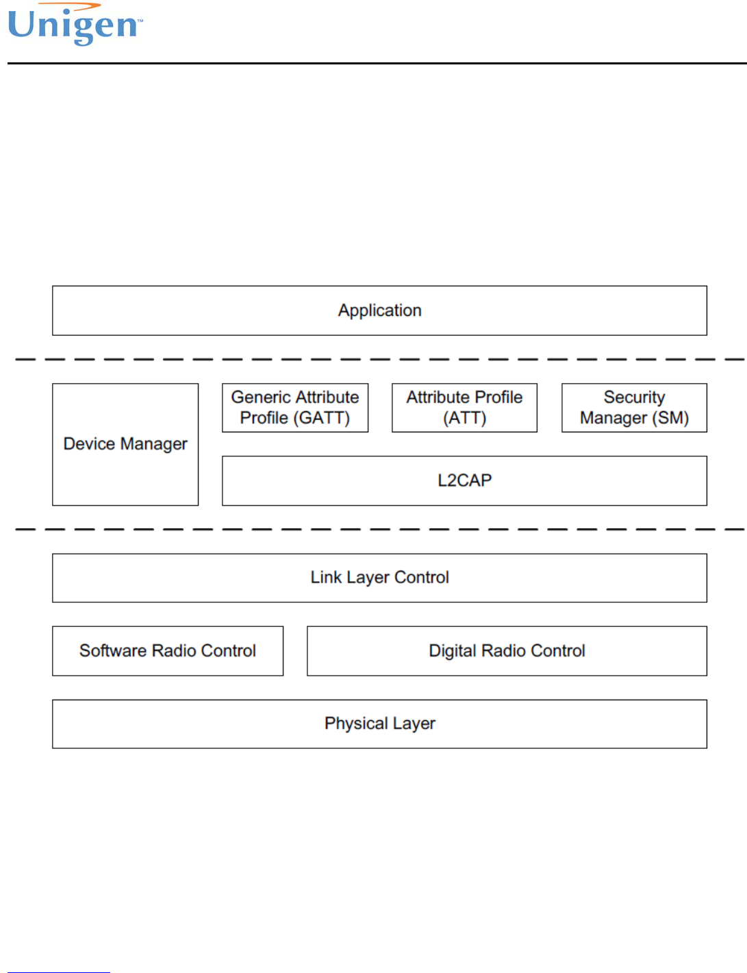
BLUETOOTH SOFTWARE STACK
The Anthias module is supplied with Bluetooth v4.0 specification compliant stack firmware which
runs on the internal RISC microcontroller. The figure below shows that the Anthias software
architecture allows Bluetooth processing and the application program to run on the internal RISC
microcontroller.
Figure 3: Anthias Bluetooth 4.0 Firmware Stack

Solutions for a Real Time World ANTHIAS BLE Module
User Manual
Re-Tek - xxxx - 17 - 45388 Warm Springs Blvd. Fremont, CA 94539
support@unigen.com TEL: (510) 668.2088 FAX: (510) 661.2788
http://www.unigen.com Customer Comment Line: (800) 826.0808
Copyright Unigen Corporation, 2012
SOFTWARE DEVELOPMENT
The Anthias uses Cambridge Silicon Radio’s CSR1000™ chipset. The RISC microcontroller is
capable of running applications to access the BTLE v4.0 software stack, serial interfaces and IOs.
Software development is through CSR’s µEnergy Integrated Development Environment (xIDE)
supplied with CSR’s μEnergy™ Software Development Kits (SDKs). The SDK is available from
either CSR or Unigen for purchase. The SDK allows the module to be utilized specifically for the
end application and product.
The xIDE allows software engineers to build and configure the application projects provided with
application specific SDKs or to independently develop applications to run on CSR’s μEnergy™ ICs
or Anthias. It supports the development and debugging of applications written in ANSI C language.
Code is written in the text editor and when complete, built and compiled along with the μEnergy™
firmware supplied as part of the SDK. When compiled the resultant machine code can be
downloaded to and run on Anthias.
The code can then be debugged on-module using the facilities in xIDE. Applications can be
developed from the reference application code provided, using the example code and library
functions supplied, to adapt and add functionality. The application source code provided
implements various Bluetooth Low Energy Profiles. These Profiles can be used as part of the
user’s own applications. Using profile code and example applications as a starting point for
development, greatly reduces the effort required to produce working Bluetooth Low Energy
applications that correctly implement the required Bluetooth Low Energy Profiles
To obtain the SDK please contact Unigen for more details.
Note:
The supplied profile code usually supports all the mandatory features and most but
not all optional features of a particular profile. See the individual SDK Release Note
for details.

Solutions for a Real Time World ANTHIAS BLE Module
User Manual
Re-Tek - xxxx - 18 - 45388 Warm Springs Blvd. Fremont, CA 94539
support@unigen.com TEL: (510) 668.2088 FAX: (510) 661.2788
http://www.unigen.com Customer Comment Line: (800) 826.0808
Copyright Unigen Corporation, 2012
MICROCONTROLLER, MEMORY, IO AND BASEBAND LOGIC
Figure 4: Microcontroller, Memory, IO, Baseband Logic Diagram
System Ram
64KB of integrated RAM supports the RISC microcontroller and is shared between the ring buffers
used to hold data for each active connection and the general-purpose memory required by the
Bluetooth stack.
Internal ROM
CSR1000™ QFN has 64KB of internal ROM. This memory is provided for system firmware
implementation. If the internal ROM holds valid program code, on boot-up, this is copied into the
program RAM.
Solutions for a Real Time World ANTHIAS BLE Module
User Manual
Re-Tek - xxxx - 19 - 45388 Warm Springs Blvd. Fremont, CA 94539
support@unigen.com TEL: (510) 668.2088 FAX: (510) 661.2788
http://www.unigen.com Customer Comment Line: (800) 826.0808
Copyright Unigen Corporation, 2012
Microcontroller
The microcontroller, interrupt controller and event timer execute the Bluetooth Low Energy
software stack and control the BLE radio and external interfaces. A 16-bit RISC microcontroller is
used for low power consumption and efficient use of memory.
Programmable I/O Ports, PIO and AIO
12 lines of programmable bidirectional I/O are provided. They are all powered from the Anthias
internal regulating circuitry. PIO lines are software-configurable as weak pull-up, weak pull-down,
strong pull-up or strong pull-down.
Note:
At reset all PIO lines are inputs with internal weak pull-downs.
Any of the PIO lines can be configured as interrupt request lines or to wake the module from
deep sleep mode. Table below lists the options for waking the module from the sleep modes.
Table 8: Wake Options
Sleep Mode Wake-up Options
Dormant Can only be woken by the WAKE pad.
Hibernate Can only be woken by the WAKE pad or by the watchdog timer.
Deep Sleep Can be woken by any PIO configured to wake the module.
The Anthias module supports alternative functions on the PIO lines:
SPI Interface
UART
LED Flasher / PWM modules
Note: Unigen cannot guarantee that all the PIO assignments remain as described.
Implementation of the PIO lines is firmware build specific. For more information,
see relevant software release note.
Anthias has 3 general purpose analog interface pads, AIO[2:0] .
Solutions for a Real Time World ANTHIAS BLE Module
User Manual
Re-Tek - xxxx - 20 - 45388 Warm Springs Blvd. Fremont, CA 94539
support@unigen.com TEL: (510) 668.2088 FAX: (510) 661.2788
http://www.unigen.com Customer Comment Line: (800) 826.0808
Copyright Unigen Corporation, 2012
LED Flasher / PWM modules
Anthias contains a LED flasher / PWM modules that work in sleep modes. These functions are
controlled by the on-chip firmware.
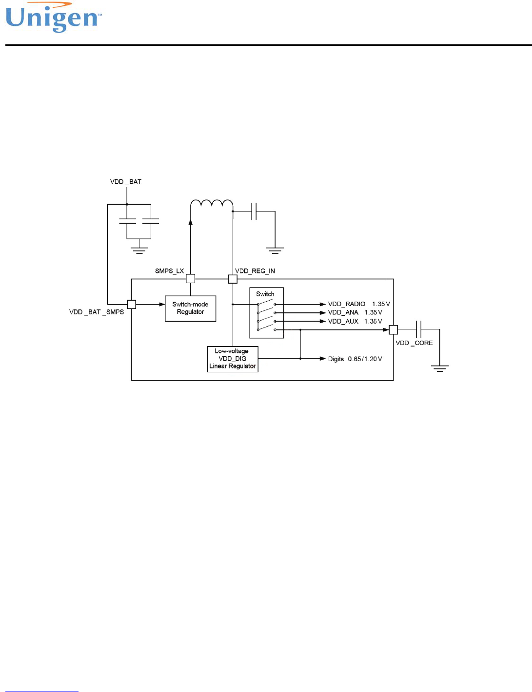
POWER CONTROL, REGULATION AND RESET
Figure 5: Anthias Internal Regulation Block
Internal Switch-mode Regulator
Anthias has an internal switch mode regulator that generates the main rail from the battery
(VDD_BAT). The main rail supplies the lower regulated voltage to a further internal digital linear
regulator and also to the analog sections of the Anthias module. The switch mode regulator
generates typically an internal 1.35V.
Internal Low-voltage Linear Regulator
The integrated low-voltage VDD_DIG linear regulator powers the Anthias digital circuits. The input
voltage range is 0.65V to 1.35V. It can supply programmable voltages of 0.65V to 1.20V to the
digital area of the Anthias module. The maximum output current for this regulator is 30mA.
Important Note:
These regulators are for internal Unigen use only. See example circuit diagram
for Unigen recommended circuit connection.
Solutions for a Real Time World ANTHIAS BLE Module
User Manual
Re-Tek - xxxx - 21 - 45388 Warm Springs Blvd. Fremont, CA 94539
support@unigen.com TEL: (510) 668.2088 FAX: (510) 661.2788
http://www.unigen.com Customer Comment Line: (800) 826.0808
Copyright Unigen Corporation, 2012
Reset
Anthias is reset by software-configured watchdog timer.
Digital Pad States on Reset
Table 9: Digital Pad State on Reset
Pad Name / Group On Reset
I2C_SDA Strong PU
I2C_SCL Strong PU
PIO[11:0] Weak PD
SERIAL INTERFACES
Application UART Interface
The Anthias UART interface provides a simple mechanism for communicating with other serial
devices using the RS232 protocol.
2 signals implement the UART function, UART_TX and UART_RX. When Anthias is connected to
another digital device, UART_RX and UART_TX transfer data between the 2 devices.
UART configuration parameters, e.g. baud rate and data format, are set using ANTHIAS
application code firmware.
When selected in firmware PIO[0] is assigned to a UART_TX output and PIO[1] is assigned to a
UART_RX input, see the module pad assignment and description for more details.
The UART CTS and UART RTS signals can be assigned to any PIO pad by the on-chip firmware.
Note: To communicate with the UART at its maximum data rate using a standard PC, the PC
requires an accelerated serial port adapter card.
Solutions for a Real Time World ANTHIAS BLE Module
User Manual
Re-Tek - xxxx - 22 - 45388 Warm Springs Blvd. Fremont, CA 94539
support@unigen.com TEL: (510) 668.2088 FAX: (510) 661.2788
http://www.unigen.com Customer Comment Line: (800) 826.0808
Copyright Unigen Corporation, 2012
The table below shows the possible UART settings for the ANTHIAS module.
Table 10: Anthias UART Parameters
Parameter Possible Values
Baud Rate Minimum 1200 baud (≤2% Error)
9600 baud (≤1% Error)
Maximum 2Mbaud (≤1% Error)
Flow Control CTS/RTS
Parity None, Odd or Even
Number of stop bits 1 or 2
Bits per byte 8
Note: The maximum baud rate during Deep Sleep is 9600 baud.
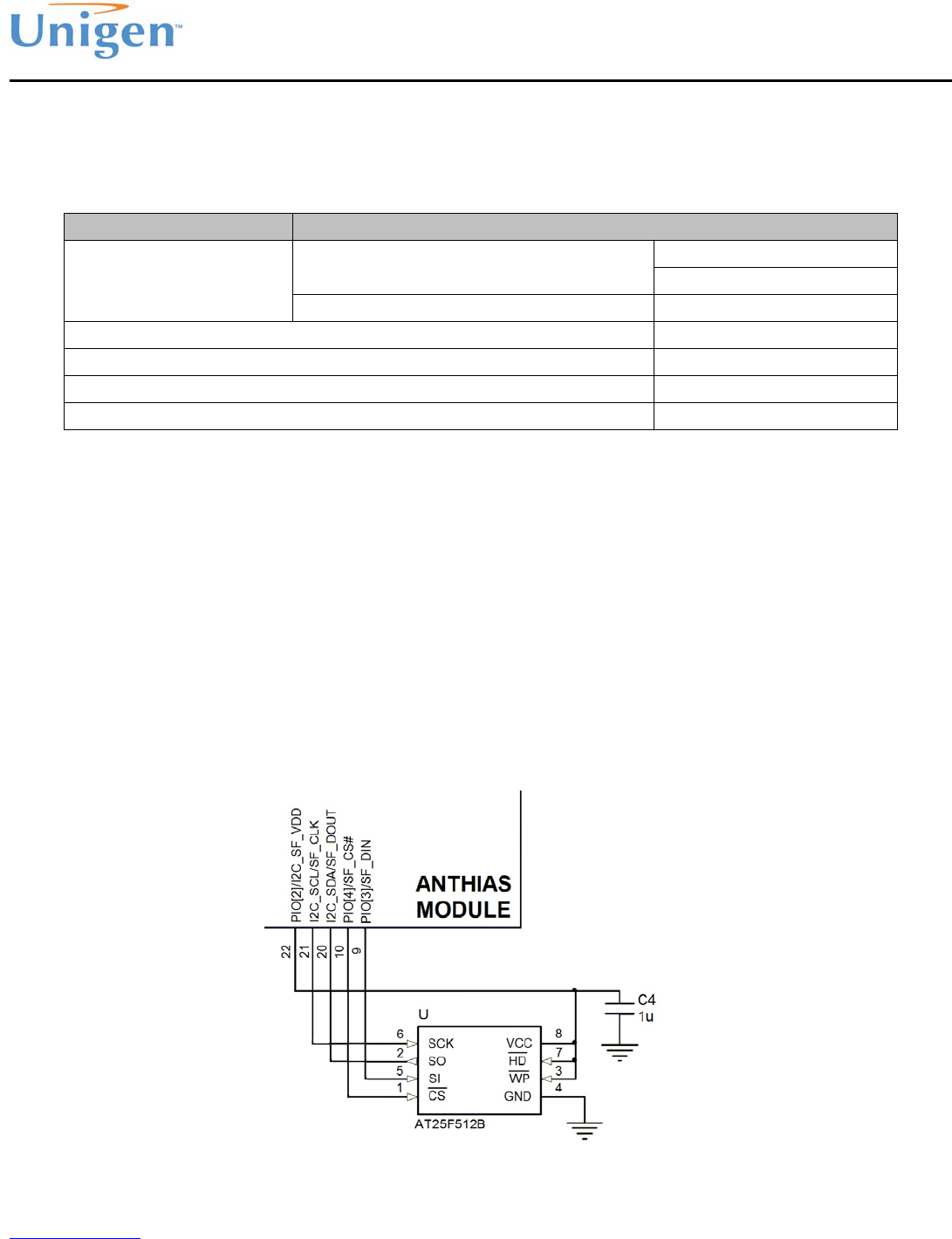
SPI Master Serial Flash Interface
The SPI Serial Flash Interface is only available if Anthias is ordered and configured without the
internal EEPROM option on the module. The SPI master memory interface in the Anthias module
is overlaid on the internal I²C EEPROM interface and uses 3 other specific PIOs for the additional
signaling. See the table on the next page for more details.
PIO[2] is used to power the Serial Flash upon boot up to read the contents and load into RAM.
After loading the contents, PIO[2] is de-asserted to shut down the Serial Flash for power savings.
Figure 6: External Serial EEPROM Circuitry
Solutions for a Real Time World ANTHIAS BLE Module
User Manual
Re-Tek - xxxx - 23 - 45388 Warm Springs Blvd. Fremont, CA 94539
support@unigen.com TEL: (510) 668.2088 FAX: (510) 661.2788
http://www.unigen.com Customer Comment Line: (800) 826.0808
Copyright Unigen Corporation, 2012
The table below shows the corresponding external Serial Flash signals when the external serial
Flash option of the Anthias module is used to store the application code.
Table 11: Anthias External Serial Flash Signals
SPI Serial Flash
Interface Pad Label Description
FLASH_VDD 22 PIO_2 / I2C_SF_VDD Programmable I/O line or I²C Serial
Flash power supply
SF_DIN 9 PIO_3 / SF_DIN Programmable I/O line or SPI serial
flash data (SF_DIN) input
SF_CS# 10 PIO_4 / SF_CS# Programmable I/O line or SPI serial
flash chip select (SF_CS#)
SF_CLK 21 I2C_SCL / SF_CLK SPI serial flash clock output (SF_CLK).
SF_DOUT 20 I2C_SDA / SF_DOUT SPI serial flash data output (SF_DOUT).
Programming and Debug Interface
Important Note:
The Anthias module debug SPI interface is available in SPI slave mode to enable an external
microcontroller to program and control the module, generally via libraries or tools supplied by
CSR/Unigen. The protocol of this interface is proprietary. The 4 SPI debug lines directly support
this function.
The SPI programs, configures and debugs the Anthias module. It is required for firmware upgrade
or debug. Ensure the 4 SPI signals are brought out to either test points or a header. If firmware
upgrading is required in the field then this interface needs to be accessible externally.
Take SPI_PIO#_SEL high to enable the SPI debug feature on PIO[8:5].
Anthias uses a 16-bit data and 16-bit address programming and debug interface. Transactions
occur when the internal processor is running or is stopped.
Data is written or read one word at a time, or the auto-increment feature is available for block
access.
Solutions for a Real Time World ANTHIAS BLE Module
User Manual
Re-Tek - xxxx - 24 - 45388 Warm Springs Blvd. Fremont, CA 94539
support@unigen.com TEL: (510) 668.2088 FAX: (510) 661.2788
http://www.unigen.com Customer Comment Line: (800) 826.0808
Copyright Unigen Corporation, 2012
Instruction Cycle
The ANTHIS module is the slave and receives commands on DEBUG_MOSI and outputs data on
DEBUG_MISO.
The table below shows the instruction cycle for a SPI transaction.
Table 12: SPI Transactions
1 Reset the SPI interface Hold DEBUG_CS# high for 2
DEBUG_CLK cycles
2 Write the command word Take DEBUG_CS# low and clock in the
8-bit command
3 Write the address Clock in the 16-bit address word
4 Write or read data words Clock in or out 16-bit data word(s)
5 Termination Take DEBUG_CS# high
With the exception of reset, DEBUG_CS# must be held low during the transaction. Data on
DEBUG_MOSI is clocked into the Anthias on the rising edge of the clock line DEBUG_CLK. When
reading, Anthias replies to the master on DEBUG_MISO with the data changing on the falling edge
of the DEBUG_CLK. The master provides the clock on DEBUG_CLK. The transaction is terminated
by taking DEBUG_CS# high.
The auto increment operation on the Anthias cuts down on the overhead of sending a command
word and the address of a register for each read or write, especially when large amounts of data
are to be transferred. The auto increment offers increased data transfer efficiency on the Anthias
module. To invoke auto increment, DEBUG_CS# is kept low, which auto increments the address,
while providing an extra 16 clock cycles for each extra word written or read.
Multi-slave Operation
Do not connect the Anthias module in a multi-slave arrangement by simple parallel connection of
slave MISO lines. When Anthias is deselected (DEBUG_CS# = 1), the DEBUG_MISO line does not
float. Instead, Anthias outputs 0 if the processor is running or 1 if it is stopped.

Solutions for a Real Time World ANTHIAS BLE Module
User Manual
Re-Tek - xxxx - 25 - 45388 Warm Springs Blvd. Fremont, CA 94539
support@unigen.com TEL: (510) 668.2088 FAX: (510) 661.2788
http://www.unigen.com Customer Comment Line: (800) 826.0808
Copyright Unigen Corporation, 2012
POWER CONSUMPTION
Table 13: Operating Power Consumption Figures
Operation Mode Description Current at 3V
Dormant
All functions are shutdown. To wake up toggle the
WAKE pad. <600nA
Hibernate
Software Enabled mode with only 32khz internal
clock and timer running. <1.5uA
Deep Sleep Software Enabled mode retaining all states <5uA
Idle
Software Enabled mode; MCU idle, all circuits on,
no BTLE connection ~1mA
TX/RX radio active Peak Transmit/Receive Radio On ~16mA (peak)
Idle Connection
Slave
Connected to remote BTLE radio, 1.28s period, no
slave latency, 150ppm clocks ~13uA avg.
Connected to remote BTLE radio, 0.5s period, no
slave latency, 150ppm clocks ~18.5uA avg.
Connected to remote BTLE radio, 0.25s period, no
slave latency, 150ppm clocks ~27uA avg.
Advertising Mode 200ms, 3 channels, connectable, 20 bytes payload ~93uA avg.
500ms, 3 channels, connectable, 20 bytes payload ~49uA avg.
Note: Measurements are from the battery.
Solutions for a Real Time World ANTHIAS BLE Module
User Manual
Re-Tek - xxxx - 26 - 45388 Warm Springs Blvd. Fremont, CA 94539
support@unigen.com TEL: (510) 668.2088 FAX: (510) 661.2788
http://www.unigen.com Customer Comment Line: (800) 826.0808
Copyright Unigen Corporation, 2012
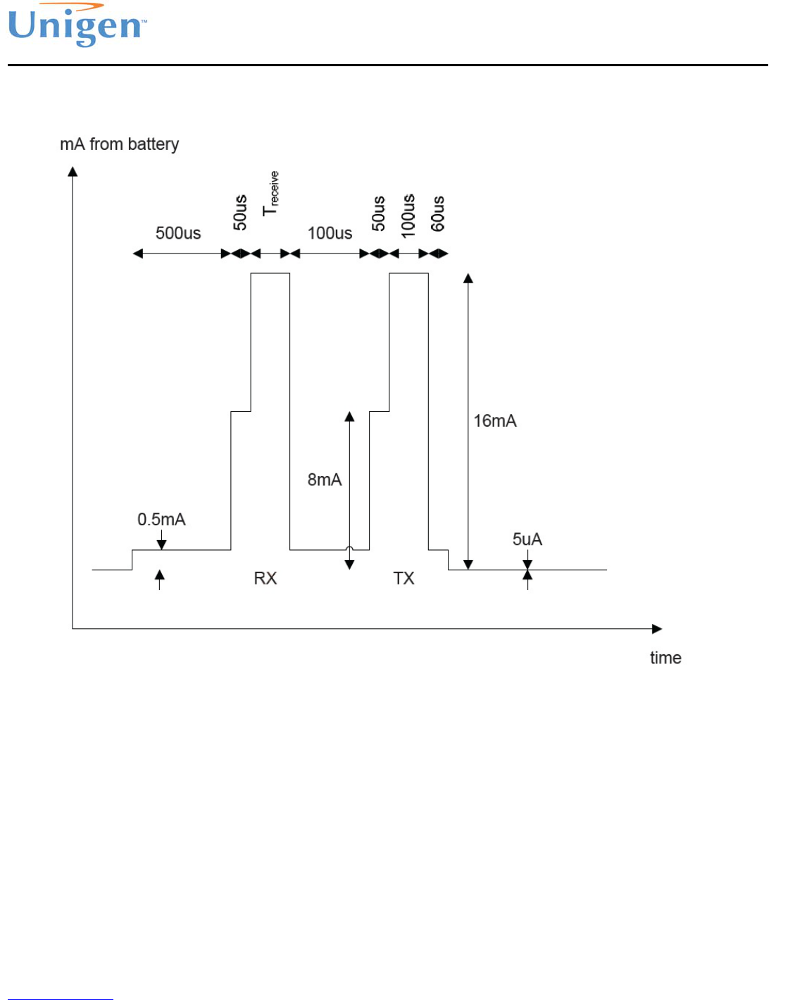
Idle Connection State as Slave
Figure 7: Idle Connection State
Treceive = 80us + (Jitter Allowance) + (Windows Widening)
Jitter Allowance = 16us
Window Widening = (Connection Interval * (Slave latency+1))*(Slave Clock Accuracy + Master
Clock Accuracy)/1e6
Radio on/off time is as important
as peak currents. Sleep clock
accuracy is vital due to window
widening between radios on/off
states.
Solutions for a Real Time World ANTHIAS BLE Module
User Manual
Re-Tek - xxxx - 27 - 45388 Warm Springs Blvd. Fremont, CA 94539
support@unigen.com TEL: (510) 668.2088 FAX: (510) 661.2788
http://www.unigen.com Customer Comment Line: (800) 826.0808
Copyright Unigen Corporation, 2012
EXAMPLE SCHEMATICS
No Serial Flash
Figure 8: Embedded EEPROM Example Schematic
Solutions for a Real Time World ANTHIAS BLE Module
User Manual
Re-Tek - xxxx - 28 - 45388 Warm Springs Blvd. Fremont, CA 94539
support@unigen.com TEL: (510) 668.2088 FAX: (510) 661.2788
http://www.unigen.com Customer Comment Line: (800) 826.0808
Copyright Unigen Corporation, 2012
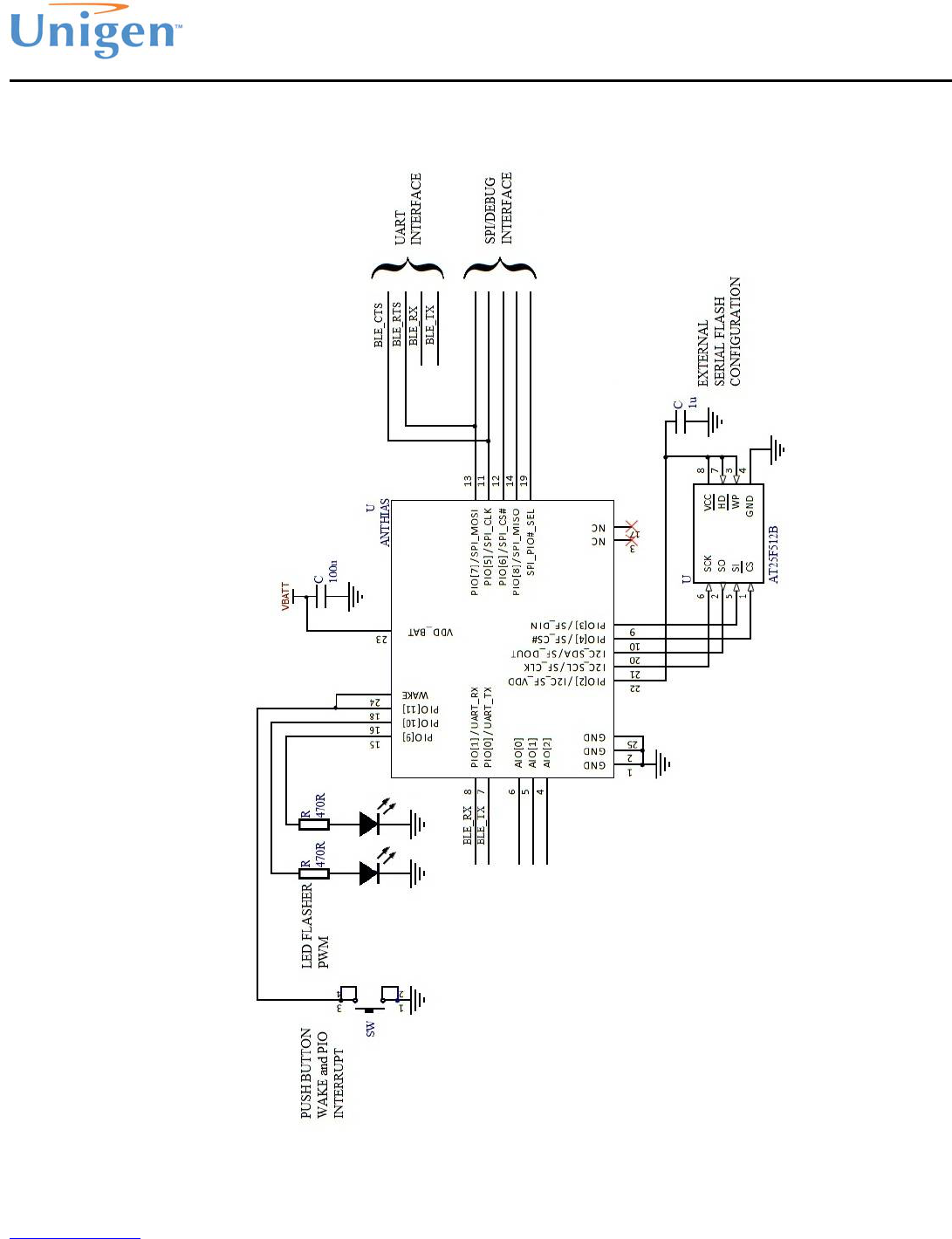
External Serial Flash Configuration
Figure 10: External Serial Flash Example Schematic
Solutions for a Real Time World ANTHIAS BLE Module
User Manual
Re-Tek - xxxx - 29 - 45388 Warm Springs Blvd. Fremont, CA 94539
support@unigen.com TEL: (510) 668.2088 FAX: (510) 661.2788
http://www.unigen.com Customer Comment Line: (800) 826.0808
Copyright Unigen Corporation, 2012
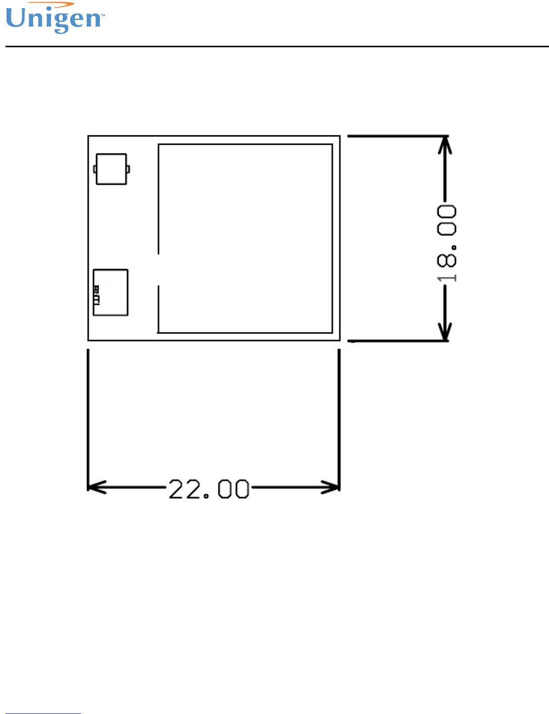
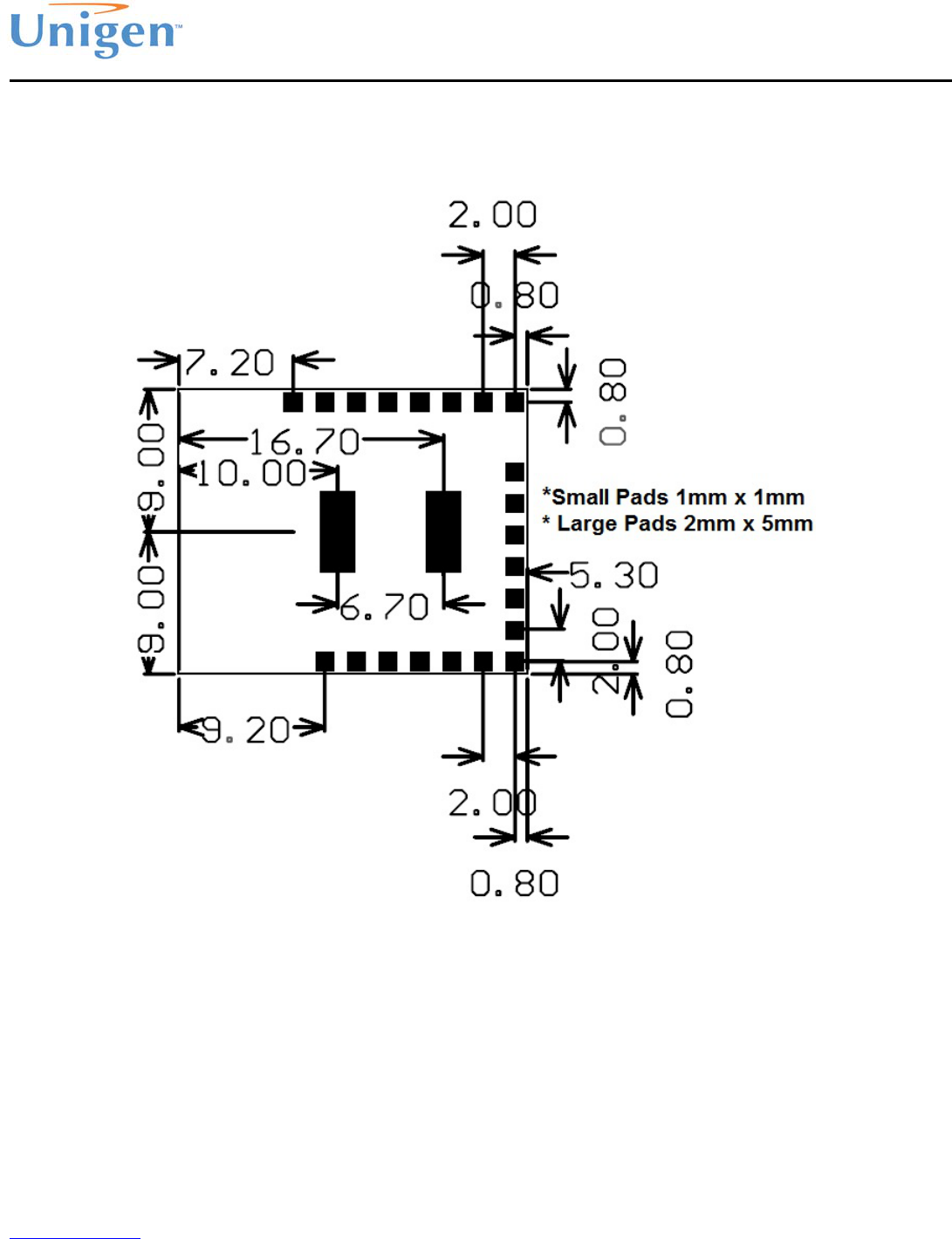
MECHANICAL DRAWINGS
Dimensions
Figure 11: ANTHIAS Mechanical Drawing
Solutions for a Real Time World ANTHIAS BLE Module
User Manual
Re-Tek - xxxx - 30 - 45388 Warm Springs Blvd. Fremont, CA 94539
support@unigen.com TEL: (510) 668.2088 FAX: (510) 661.2788
http://www.unigen.com Customer Comment Line: (800) 826.0808
Copyright Unigen Corporation, 2012
LGA Pads and Landing Pattern
Figure 12: Landing Pattern
Solutions for a Real Time World ANTHIAS BLE Module
User Manual
Re-Tek - xxxx - 31 - 45388 Warm Springs Blvd. Fremont, CA 94539
support@unigen.com TEL: (510) 668.2088 FAX: (510) 661.2788
http://www.unigen.com Customer Comment Line: (800) 826.0808
Copyright Unigen Corporation, 2012
ORDERING INFORMATION
Table 14: Part Numbers
Part Number Description
UGWANBL2SME133A Embedded EEPROM, Chip Antenna
UGWANBL2SME133U Embedded EEPROM, RF mini-coaxial connector
UGWANBL2SM0033A.EXT No EEPROM, Chip Antenna
UGWANBL2SM0033U.EXT No EEPROM, RF mini-coaxial connector
CONTACT INFORMATION
CORPORATE HEADQUARTERS
Unigen Corporation
45388 Warm Springs Boulevard
Fremont, CA 94539
Telephone: 1 (510) 688-2088
Fax: 1 (510) 668-2788
Email: Support@unigen.com
Web: www.unigen.com
Toll Free:1 (800) 826-0808

Solutions for a Real Time World ANTHIAS BLE Module
User Manual
Re-Tek - xxxx - 32 - 45388 Warm Springs Blvd. Fremont, CA 94539
support@unigen.com TEL: (510) 668.2088 FAX: (510) 661.2788
http://www.unigen.com Customer Comment Line: (800) 826.0808
Copyright Unigen Corporation, 2012
RF Radiation Hazard Warning (RSS-102, FCC)
“To ensure compliance with FCC and Industry Canada RF exposure requirements, this device must be
installed in a location where the antennas of the device will have a minimum distance of at least 20
cm from all persons. Using higher gain antennas and types of antennas not certified for use with this
product is not allowed. The device shall not be co-located with another transmitter.”
French – “Installez l'appareil en veillant à conserver une distance d'au moins 20 cm entre les
éléments rayonnants et les personnes. Cet avertissement de sécurité est conforme aux limites
d'exposition définies par la norme CNR-102 at relative aux fréquences radio.”
Antenna Limitations (RSS-GEN)
Per RSS-GEN, section 7.1.2 – “Under Industry Canada regulations, this radio transmitter may only
operate using an antenna of type and maximum (or lesser) gain approved for the transmitter by
Industry Canada. To reduce potential radio interference to other users, the antenna type and its gain
should be so chosen that the equivalent isotropically radiated power (e.i.r.p.) is not more than that
necessary for successful communication.”
French – “Conformément à la réglementation d'Industrie Canada, le présent émetteur radio peut
fonctionner avec une antenne d'un type et d'un gain maximal (ou inférieur) approuvé pour l'émetteur
par Industrie Canada. Dans le but de réduire les risques de brouillage radioélectrique à l'intention des
autres utilisateurs, il faut choisir le type d'antenne et son gain de sorte que la puissance isotrope
rayonnée équivalente (p.i.r.e.) ne dépasse pas l'intensité nécessaire à l'établissement d'une
communication satisfaisante.”
Per RSS-GEN, section 7.1.2 (detachable antennas)– “This radio transmitter has been approved by
Industry Canada to operate with the antenna types listed below with the maximum permissible gain
and required antenna impedance for each antenna type indicated. Antenna types not included in this
list, having a gain greater than the maximum gain indicated for that type, are strictly prohibited for
use with this device.”
Fench – “Le présent émetteur radio a été approuvé par Industrie Canada pour fonctionner avec les
types d'antenne énumérés ci-dessous et ayant un gain admissible maximal et l'impédance requise
pour chaque type d'antenne. Les types d'antenne non inclus dans cette liste, ou dont le gain est
supérieur au gain maximal indiqué, sont strictement interdits pour l'exploitation de l'émetteur”.

Solutions for a Real Time World ANTHIAS BLE Module
User Manual
Re-Tek - xxxx - 33 - 45388 Warm Springs Blvd. Fremont, CA 94539
support@unigen.com TEL: (510) 668.2088 FAX: (510) 661.2788
http://www.unigen.com Customer Comment Line: (800) 826.0808
Copyright Unigen Corporation, 2012
General Two Part Statement (RSS-Gen, section 7.1.3):
This device complies with Industry Canada licence-exempt RSS standard(s). Operation is subject to
the following two conditions: (1) this device may not cause interference, and (2) this device must
accept any interference, including interference that may cause undesired operation of the device.
Le présent appareil est conforme aux CNR d'Industrie Canada applicables aux appareils radio
exempts de licence. L'exploitation est autorisée aux deux conditions suivantes : (1) l'appareil ne doit
pas produire de brouillage, et (2) l'utilisateur de l'appareil doit accepter tout brouillage radioélectrique
subi, même si le brouillage est susceptible d'en compromettre le fonctionnement.
Two Part Statement (FCC, 15.19) – If not on the label, then it must be in the user’s
manual
This device complies with Part 15 of the FCC Rules. Operation is subject to the following two
conditions: (1) This device may not cause harmful interference, and (2) this device must accept any
interference received, including interference that may cause undesired operation.
Non-modification statement (FCC, 15.21) –
User’s manual shall caution the user the changes or modifications not expressly approved by
<<Company>> could void the user’s authority to operate the equipment.
Modular Requirements -
The manual for the module must instruct the integrator how to properly label the end product and
what statements must be in the user’s manual.
Label for host product:
“Contains FCC ID: R8KUGWANBL2”
“Contains IC: 5125A-UGWANBL2”