Unigen UGWC821R NEMO BLUETOOTH RADIO MODULE User Manual NEMO2 Design Guidelines
Unigen Corporation NEMO BLUETOOTH RADIO MODULE NEMO2 Design Guidelines
Unigen >
Contents
- 1. user manual
- 2. user manual design guidelines
user manual design guidelines

Solutions for a Real Time World NEMO2 Design Guidelines
Applicationnote
Unigen Corp. Wireless Module Products
NEMO Bluetooth Radio Modules
UGWC821RSMA133
Design Guidelines Application Note
Issue Date: April 3rd, 2012
Revision: 1.0

Solutions for a Real Time World NEMO2 Design Guidelines
Applicationnote
CONTENTS
Contents........................................................................................................................................................2
ListofFigures................................................................................................................................................4
ListofTables.................................................................................................................................................5
Scope.............................................................................................................................................................6
FCCTransmitterModularApprovalIntroduction.........................................................................................6
Class2PermissiveChanges...........................................................................................................................7
NEMO2ModuleGeneralDescription...........................................................................................................7
CSRBlueCore6ROMTransceiverIC.............................................................................................................8
FunctionalBlockDiagrams............................................................................................................................9
Nemo2LGAFormFactor.............................................................................................................................12
LGAPadsandAssignments.....................................................................................................................12
Nemo2ReferenceEvaluationBoard...........................................................................................................14
Nemo2EvaluationBoardBOM...............................................................................................................16
PCBLayout..............................................................................................................................................17
ComponentLayout..................................................................................................................................17
TopLayer(Layer1)..................................................................................................................................18
GroundLayer(Layer2)...........................................................................................................................18
VDDLayer(Layer3).................................................................................................................................19
BottomLayer(Layer4)............................................................................................................................20
PCBStack,Materials,Drill&Notes.........................................................................................................21
NEMO2DesignIntegrationRules...............................................................................................................22
IntendedUse...........................................................................................................................................22

Solutions for a Real Time World NEMO2 Design Guidelines
Applicationnote
Antenna&ExternalRFPath....................................................................................................................24
MicrostripTransmissionLineSpecification............................................................................................25
MicrostripPCBBoardDetails:.................................................................................................................26
MicrostripGroundReference.................................................................................................................26
RFShielding.............................................................................................................................................29
SupportContact......................................................................................................................................31

Solutions for a Real Time World NEMO2 Design Guidelines
Applicationnote
LIST OF FIGURES
Figure1:Nemo2BasicBlockDiagram..........................................................................................................9
Figure2:CSRBlueCore6ChipsetBlockDiagram........................................................................................10
Figure3:NEMO2ElaborateBlockDiagram................................................................................................11
Figure4:NEMO2LGAPads.........................................................................................................................12
Figure5:NEMO2Evaluationboard............................................................................................................14
Figure6:NEMO2EvaluationBoardComponentLayout.............................................................................17
Figure7:NEMO2EvaluationBoardTopLayer1.........................................................................................18
Figure8:NEMO2EvaluationBoardGroundLayer2...................................................................................18
Figure9:NEMO2PowerPlaneLayer3.......................................................................................................19
Figure10:NEMO2BottomSignalLayer4...................................................................................................20
Figure11:NEMO2EvaluationBoardPCBStackUp....................................................................................21
Figure12:NEMO2EvaluationBoardDrillChart.........................................................................................22
Figure13:NEMO2BluetoothSoftwareStackArchitecture........................................................................23
Figure14:NEMO2MicrostripDimensionDetails.......................................................................................25
Figure15:NEMO2EvaluationMicrostripPCBStackUPDetails.................................................................26
Figure16:NEMO2MicrostripGroundReference.......................................................................................27
Figure17:NEMO2GroundingTechnique,GroundStitchingandAdjacentGroundLayer.........................27
Figure18:GroundingConsiderations.........................................................................................................28
Figure19:NEMO2EvaluationBoardExampleShield.................................................................................29
Figure20:NEMO2EvaluationBoardTopSoldermaskRFShieldOutline...................................................30
Figure21:NEMO2EvaluationBoardRFShieldMicrostripgapspacing.....................................................30

Solutions for a Real Time World NEMO2 Design Guidelines
Applicationnote
LIST OF TABLES
Table1:NEMO2LGAPadDescription........................................................................................................13
Table2:NEMO2EvaluationBoardBOM.....................................................................................................16

Solutions for a Real Time World NEMO2 Design Guidelines
Applicationnote
SCOPE
The purpose of this document is to describe the functionality, operation, specific
design restrictions and guidelines of the NEMO2 module for integration and
regulatory/certification explanation with approved partners. Design integration is
important to comply with FCC/IC regulatory limited module approvals. The NEMO2
evaluation board will be used as an example and reference to modular approvals on
transmission line and antennas.
FCC TRANSMITTER MODULAR APPROVAL INTRODUCTION
A transmitter with a modular or limited modular grant can be installed in different
end-use products (referred to as a host, host product, or host device) by the
grantee or other equipment manufacturer; and the host may not require additional
testing or equipment authorization for the transmitter function provided by that
specific module or limited module.
NEMO2 has received Limited Modular Approval and each OEM will be
required to have Radiated Emissions measured to ensure compliance.
A host product incorporating a certified device cannot take advantage of the pre-
existing certification of the component transmitter module without conformity with
these specific requirements. Modular approvals are for tangible, clearly delineated,
devices that operate when installed within, or attached to, a host in one of the
following four physical configurations:
1. Single-modular transmitter: a complete RF transmission sub-assembly,
designed to be incorporated into another device, that must demonstrate
compliance with FCC rules and policies independent of any host;
2. Limited single-modular transmitter: a single-modular transmitter that
complies with the Section 15.212(a)(1) modular rules, only when constrained
to specific operating host(s) and/or associated grants condition(s);
3. Split-modular transmitter: a RF transmission system that complies with
the requirements for a single-modular transmitter, that is separated into a
radio front-end section and a control-element section, and can demonstrate
compliance for a range of similar type hosts;

Solutions for a Real Time World NEMO2 Design Guidelines
Applicationnote
4. Limited split-modular transmitter: a split-modular transmitter that
complies with the definition and technical rules for split modules only when
constrained to specific operating host(s), and/or associated grant
condition(s).
A host product is required to comply with all applicable FCC equipment
authorizations regulations, requirements and equipment functions not associated
with the transmitter module portion. For example, compliance must be
demonstrated to regulations for other transmitter components within the host
product; to requirements for unintentional radiators (Part 15B), such as digital
devices, computer peripherals, radio receivers, etc.; and to additional authorization
requirements for the non-transmitter functions on the transmitter module (i.e.,
Verification, or Declaration of Conformity) (e.g., Bluetooth and WiFi transmitter
modules may also contain digital logic functions) as appropriate.
To ensure compliance with all non-transmitter functions the host manufacturer is
responsible for ensuring compliance with the module(s) installed and fully
operational. For example, if a host was previously authorized as an unintentional
radiator under the Declaration of Conformity procedure without a transmitter
certified module and a module is added, the host manufacturer is responsible for
ensuring that the after the module is installed and operational the host continues to
be compliant with the Part 15B unintentional radiator requirements. Since this may
depend on the details of how the module is integrated with the host, the grantee
(the party responsible for the module grant) shall provide guidance to the host
manufacturer for compliance with the Part 15B4 requirements.
CLASS 2 PERMISSIVE CHANGES
NEMO2 is not equipped with a permanently attached antenna or unique antenna
connector. The integrator can choose to use the same antenna, connector and
microstrip transmission line in the end product design. However, any changes to this
RF path will require retesting on the radiated portion and a Class II permissive
change to utilize part of the modular Unigen grant. For more information on Class II
permissive change and processes, please inquire your regulatory TCB.
NEMO2 MODULE GENERAL DESCRIPTION

Solutions for a Real Time World NEMO2 Design Guidelines
Applicationnote
The Nemo2 module is a complete Bluetooth 2.4GHz radio transceiver operating in
the license free ISM (Industrial, Scientific and Medical) band. The Nemo module has
CSR’s BlueCore 6 ROM Bluetooth solution. The CSR BlueCore 6 ROM is a single-chip
radio and baseband IC for Bluetooth 2.4GHz systems including enhanced data rate
(EDR) to 3Mbps. With the on-chip CSR Bluetooth software stack, it provides a fully
compliant Bluetooth v2.1 + EDR specification system for data and voice
communications. The Nemo2 is a complete separate PCBA module with dimensions
measure 6.5mm x 6.5mm x 1.5mm. A single 3.3V power supply input, single ended
RF output/input, and a low 26 pad count makes the NEMO module easy to interface
with. The module contains on board supply regulation, radio crystal oscillator,
BALUN and bandpass filter.
CSR BLUECORE 6 ROM TRANSCEIVER IC
BlueCore™6-ROM is a single-chip transceiver radio and baseband IC for Bluetooth
2.4 GHz systems. With the on-chip CSR Bluetooth software stack, it provides a fully
compliant Bluetooth system to v2.1 of the specification for data and voice
communications with buffered modulation/data inputs to ensure that the device will
comply with Part 15 requirements with any type of input signal.
The device incorporates auto-calibration and built-in self-test (BIST) routines to
simplify development, type approval and production test. All hardware and device
firmware is fully compliant with the Bluetooth v2.1 +EDR specification (all
mandatory and optional features).
Solutions for a Real Time World NEMO2 Design Guidelines
Applicationnote
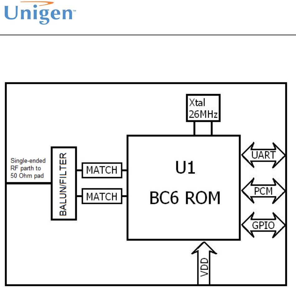
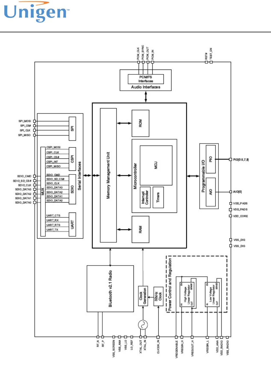
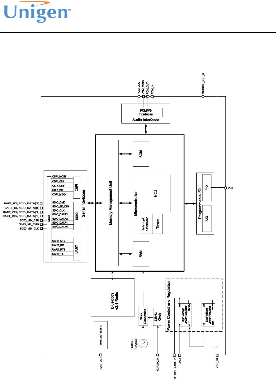
FUNCTIONAL BLOCK DIAGRAMS
Figure1:Nemo2BasicBlockDiagram
Solutions for a Real Time World NEMO2 Design Guidelines
Applicationnote
Figure2:CSRBlueCore6ChipsetBlockDiagram
Solutions for a Real Time World NEMO2 Design Guidelines
Applicationnote
Figure3:NEMO2ElaborateBlockDiagram
Solutions for a Real Time World NEMO2 Design Guidelines
Applicationnote
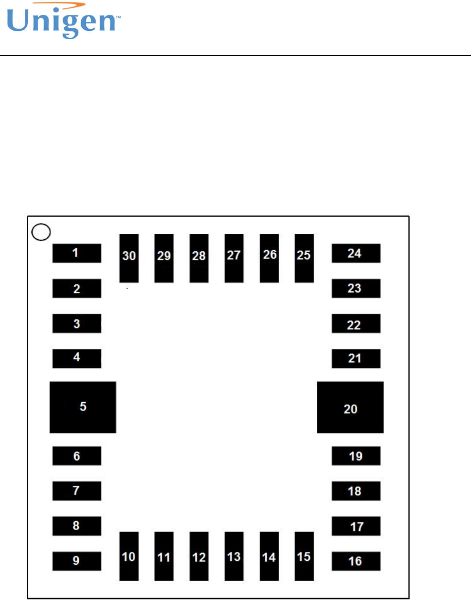
NEMO2 LGA FORM FACTOR
Nemo2 is a 26 pad LGA surface mount LGA module. The 26 pads interfaces the
module to a host and host PCB with power supply, ground, digital UART
communications, regulator enable, PCM audio bus, digital PIOs and single RF output.
LGA Pads and Assignments
Figure4:NEMO2LGAPads
Solutions for a Real Time World NEMO2 Design Guidelines
Applicationnote
Table1:NEMO2LGAPadDescription
Pin Signal Name Type Description
1 CLK32K_IN Input
32.768kHz low power clock
input
2 SDIO_SD_CSB Input SDIO Interface/Enable
3 SDIO_SD_CMD -- SDIO Interface
4 SDIO_SD_CLK -- SDIO Interface
5 GND -- Ground Reference
6 PIO(0) I/O I/O or WiFi- Coex signal
7 PIO(1) I/O I/O or WiFi- Coex signal
8 PIO(4) I/O I/O or WiFi- Coex signal
9 PIO(5) I/O I/O or WiFi- Coex signal
10 PIO(7) I/O I/O
11 GND -- Ground Reference
12 GND -- Ground Reference
13 ANT_OUT -- Antenna Output
14 GND -- Ground Reference
15 GND -- Ground Reference
16 PCM_CLK -- PCM Interface
17 PCM_OUT -- PCM Interface
18 PCM_IN -- PCM Interface
19 PCM_SYNC -- PCM Interface
20 GND -- Ground Reference
21 UART_RX/SDIO_DATA[2] I/O UART/SDIO_DATA Interface
22 UART_RTS/SDIO_DATA[1] I/O UART/SDIO_DATA Interface
23 UARTCTS/SDIO_DATA[3] I/O UART/SDIO_DATA Interface
24 UART_TX/SDIO_DATA[0] I/O UART/SDIO_DATA Interface
25 GND -- Ground Reference
26 BT_REG_CTRL_P PWR Internal Regulator Enable.
27 3V3 PWR PWR Supply
28 3V3 PWR PWR Supply
29 MODULE_RST_N Input Module Reset
30 VDD_RF -- Output of Internal Regulator
Note: Active Low signals are designated with an '_N' suffix, and Active High signals are designated
with an '_P' suffix.
Solutions for a Real Time World NEMO2 Design Guidelines
Applicationnote
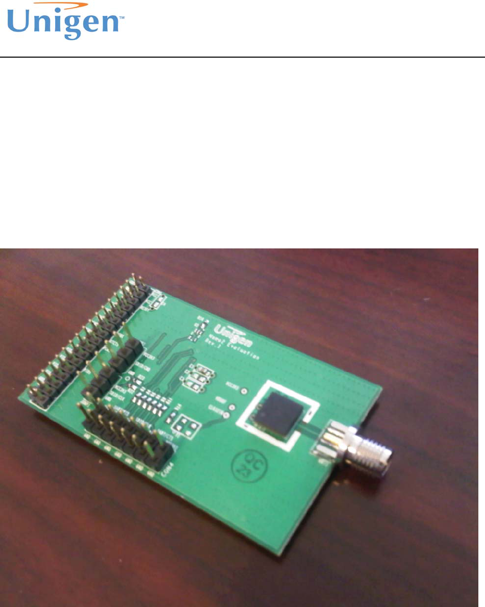
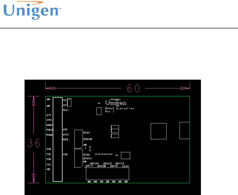
NEMO2 REFERENCE EVALUATION BOARD
The Nemo2 reference evaluation board is used for testing and evaluation of the
Nemo2 product for performance testing, application evaluation, software testing and
RF performance testing. The Nemo2 reference evaluation board was also used for
Bluetooth, FCC, IC and ETSI certification testing. The Nemo2 is a reference example
design and the physical design and rules should be taken into consideration of the
integrator of the Nemo2 module.
Design files are available from Unigen upon request.
Figure5:NEMO2Evaluationboard
Solutions for a Real Time World NEMO2 Design Guidelines
Applicationnote
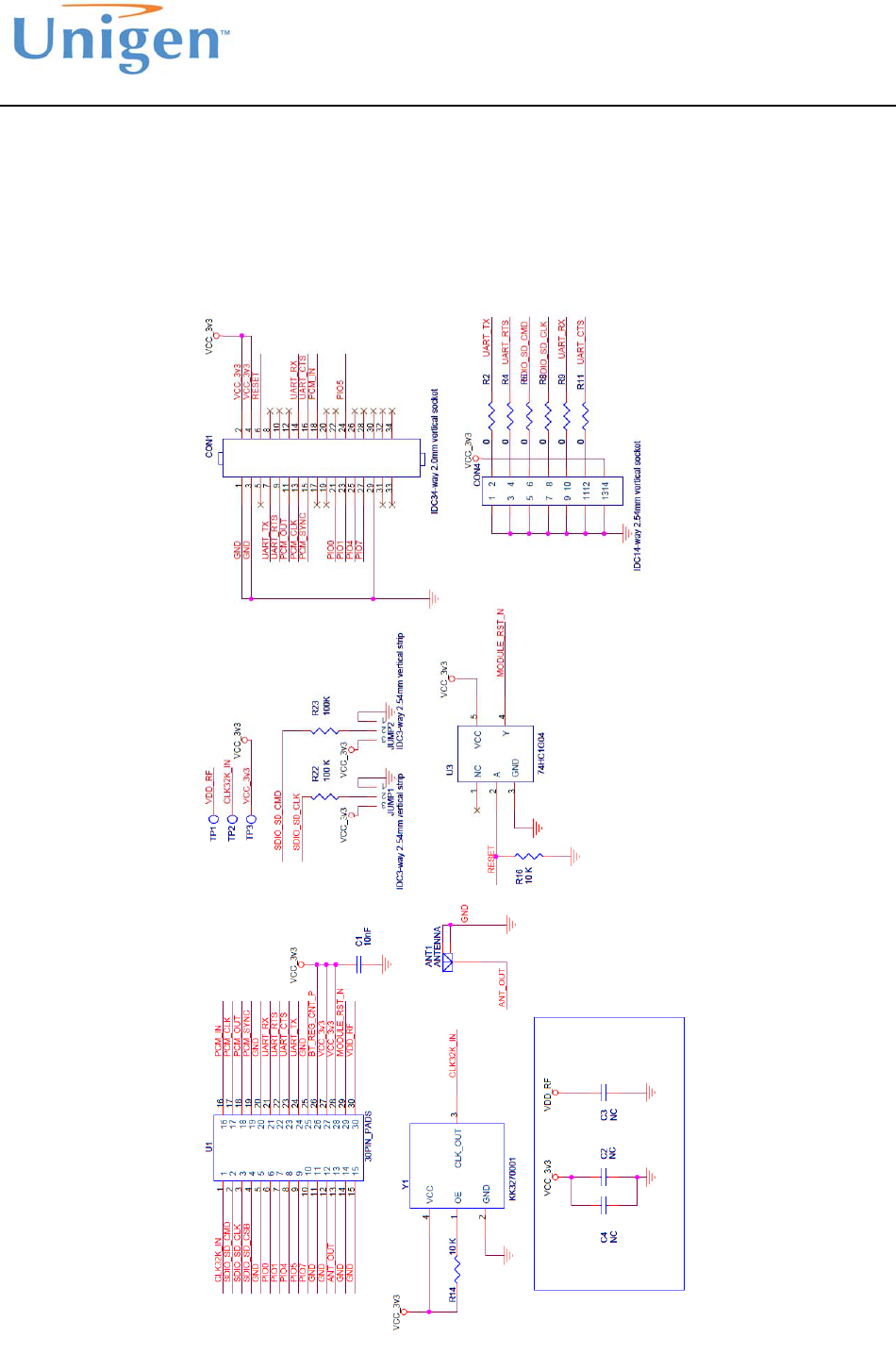
Schematic
Solutions for a Real Time World NEMO2 Design Guidelines
Applicationnote
Nemo2 Evaluation Board BOM
Table2:NEMO2EvaluationBoardBOM
Description Qty
Reference
Designator Part Number(s) Manufacturer (s)
CONN SMA FEMALE EDGE MOUNT
0.031IN THK BD 1.0 ANT1 CONREVSMA003.031
LINX
TECHNOLOGIES
CONN HDR 3POS 2.54MM AU VERT TH 2.0 JUMP1,JUMP2 TSW-103-07-G-S SAMTEC
CONN HDR 7x2 2.54MM VERT THRU-
HOLE 1 CON4 TSW-107-07-G-D SAMTEC
CONN SOCKET 17x2 2MM SQ TAIL TH 1.0 CON1 SQT-117-03-L-D SAMTEC
RES 0 OHM JUMPER 1/16W 0402 6.0 R2,R4,R6,R8,R9,R11
RC0402JR-070RL,
CRCW04020000Z0ED,
WR04X000PTL,
ERJ-2GE0R00X
YAGEO,
VISHAY,
WALSIN,
PANASONIC
RES 100K OHM 1/16W 5% 0402 2.0 R22,R23 ERJ-2GEJ104X PANASONIC
RES 10K OHM 1/16W 5% 0402 2.0 R14,R16 MCR01MZPJ103 ROHM
CAP CER 0.01UF 5% 50V X7R 0603 1.0 C1 0603B103J500CT WALSIN
NEMO2 1.0 U1 UGWC821RSMA133 Unigen
Solutions for a Real Time World NEMO2 Design Guidelines
Applicationnote
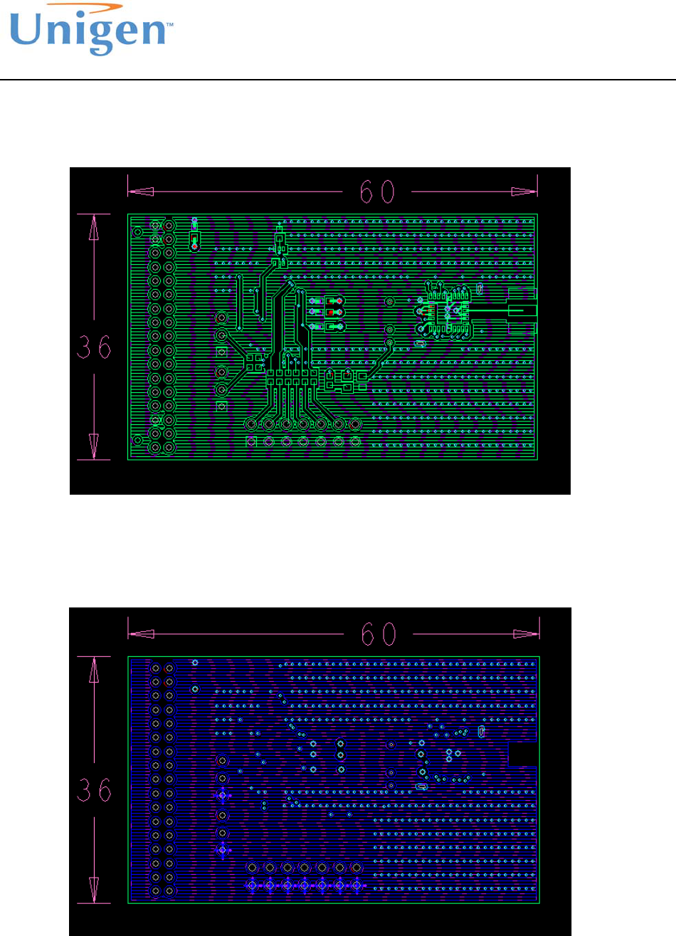
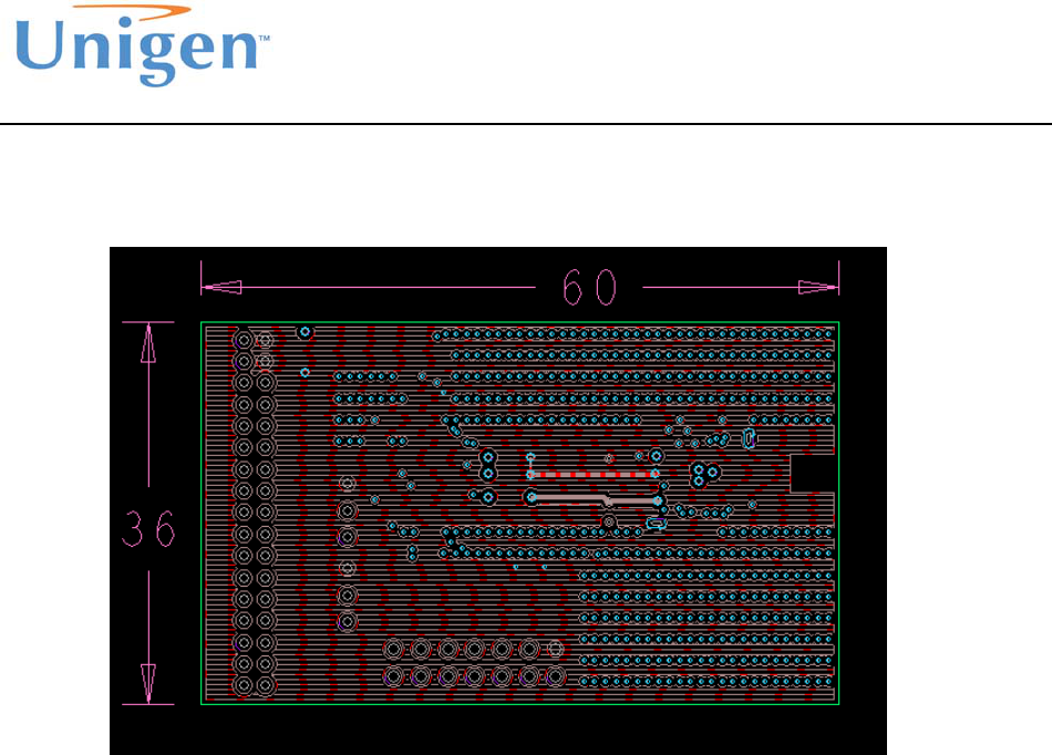
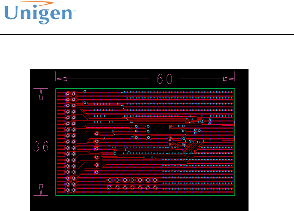
PCB Layout
Component Layout
Figure6:NEMO2EvaluationBoardComponentLayout
Solutions for a Real Time World NEMO2 Design Guidelines
Applicationnote
Top Layer (Layer 1)
Figure7:NEMO2EvaluationBoardTopLayer1
Ground Layer (Layer 2)
Figure8:NEMO2EvaluationBoardGroundLayer2
Solutions for a Real Time World NEMO2 Design Guidelines
Applicationnote
VDD Layer (Layer 3)
Figure9:NEMO2PowerPlaneLayer3
Solutions for a Real Time World NEMO2 Design Guidelines
Applicationnote
Bottom Layer (Layer 4)
Figure10:NEMO2BottomSignalLayer4
Solutions for a Real Time World NEMO2 Design Guidelines
Applicationnote
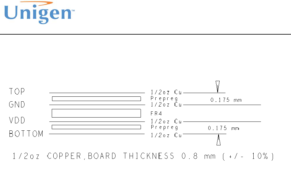
PCB Stack, Materials, Drill & Notes
Figure11:NEMO2EvaluationBoardPCBStackUp
NOTES:
1.) Material:
a. Epoxy glass laminate and prepreg. Type, Standard FR4. Finished external
layer 1 oz copper
b. Finished thickness 0.8 ± 5%mm
2.) Drilling:
a. Diameters in drill table are finished hole sizes, tolerance ± 0.0762mm.
b. Teardrop allowed on entry of via on every trace layer
3.) Final Fabrication:
a. Soldermask primary and secondary side of the board using liquid
photoimagable mask material over bare copper per IPC-SM840. Mask
artworks provided are 1:1. Solder mask color “GREEN”
4.) Copper Finish shall be immersion silver (2 ~ 8 u)
5.) Manufacture board to be in accordance with performance standard IPC-A-
6011/6012 Class 2.
6.) Maximum warp or twist shall not exceed 1%
7.) PCB shall be RoHS and WEE compliance directive 2002/95/EC
8.) Board outline dimension tolerance ± 0.13mm unless otherwise specified.
Solutions for a Real Time World NEMO2 Design Guidelines
Applicationnote
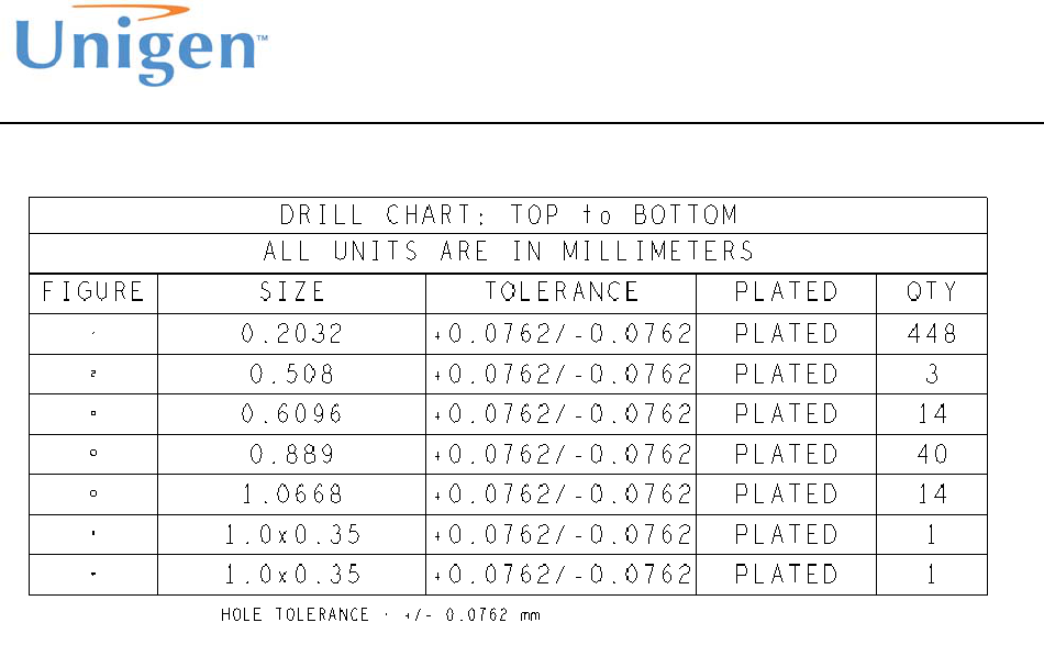
Figure12:NEMO2EvaluationBoardDrillChart
NEMO 2 DESIGN INTEGRATION RULES
Nemo2 meets regulatory modular certifications. The use of Nemo2 and integration is
important and shall be used for its intended purposes. The use of Nemo2 and
integration outside of Unigen’s design rules and use void any certifications with the
module or require permissive change and additional testing to meet certifications.
Intended Use
Application
Nemo2 is intended to be used for Bluetooth applications only. Bluetooth applications
may apply to consumer products, mobile, computing, audio applications, and other
various Bluetooth end user applications. The use of Nemo2 outside of Bluetooth
application is strictly prohibited and all Bluetooth and regulatory certifications will be
voided.
Solutions for a Real Time World NEMO2 Design Guidelines
Applicationnote
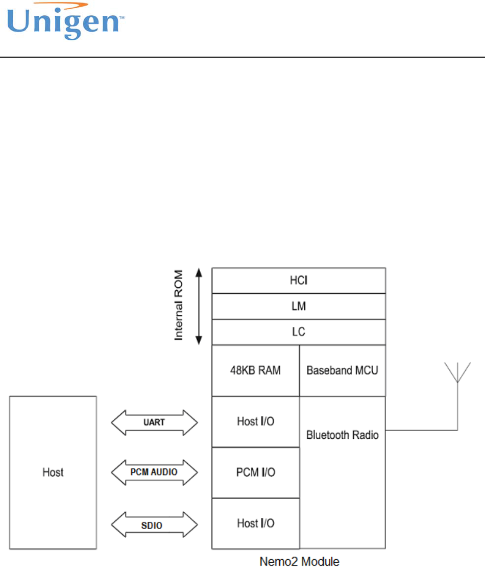
Software and Host
Nemo2 is intended to operate with a host. The host will communicate to the module
via the physical communication interfaces, UART/SDIO, to control the modules RF
operating behavior. The host shall run the Bluetooth Upper software protocol stack
operate Nemo2 in Bluetooth modes only. Nemo2 is not intended to operate without
a host and Bluetooth protocol stack. The Nemo2 software interface is based on the
Bluetooth Host Controller Interface Transport Layer specification (HCI). For more
details on the Bluetooth HCI protocol layer, please see the latest Bluetooth
Specification (3.0+HS), volume 4 and the section pertaining to Host Controller
Interface [Transport Layer]
Figure13:NEMO2BluetoothSoftwareStackArchitecture

Solutions for a Real Time World NEMO2 Design Guidelines
Applicationnote
Antenna & External RF Path
Nemo2 is not shipped with an on board antenna and an antenna is not fixed on the
module. It is the integrators responsibility to handle the design of the antenna design of
their product when using Nemo2.
NEMO2 was tested and qualified with a 2.4GHz, external, reverse SMA, di-pole, one-
quarter wave length antenna connected to a reverse SMA RF connectors and a
microstrip transmission line on the Nemo2 evaluation reference board. Any change of
antenna, RF connector or miscrostip transmission line characteristics used other than
the Nemo2 reference evaluation board may require retesting of radiated portion of the
FCC part 15B specification and will require a Class II permissive change.
NEMO2 has a single ended RF pad on the bottom of the module. The pad impedance is
50 ohms. The integrator must take care on using a microstrip transmission line for the
RF signal out. Extra care is needed on the design of the microstrip and must adhere to
Unigen’s design integration rules. The termination of the path can be a matched
antenna (printed or component) or can terminate to a RF connector (U.FL, GSC, SMA,
etc).
Antenna specifications:
Manufacturer: Pulse
Part Number: W1030
Frequency: 2.4GHz – 2.5GHz
Gain: 2.0dBi
Impedance: 50Ω
VSWR: ≤ 2.0
Polarization: Vertical
Electrical Length: ¼ wave, di-pole
Radiation: Omni
Solutions for a Real Time World NEMO2 Design Guidelines
Applicationnote
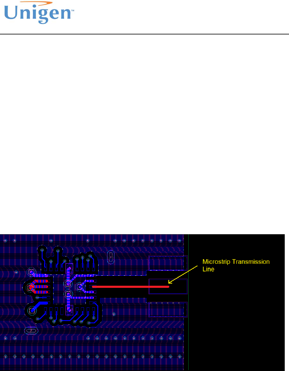
Microstrip Transmission Line Specification
The Nemo2 module requires a Microstrip transmission line on the integrators PCB
motherboard to route the RF path to an antenna or RF connector. The microstrip on
the Nemo2 reference evaluation board was used during testing and certifications.
The integrator shall use the exact Microstrip transmission line on the reference
evaluation board in the integrators product/design. The same Microstrip
transmission line can feed into any RF connector or antenna. However, any change
of antenna, RF connector or miscrostip transmission line characteristics used other
than the Nemo2 reference evaluation board may require retesting of radiated
portion of the FCC part 15B specification and will require a Class II permissive
change. Design files of the Nemo2 reference evaluation board are available in
GERBER format from Unigen.
Microstrip Dimension Details:
Length: 8.20mm
Width: 0.25mm
Impedance: 50 Ohms
Figure14:NEMO2MicrostripDimensionDetails
Solutions for a Real Time World NEMO2 Design Guidelines
Applicationnote
Microstrip PCB Board Details:
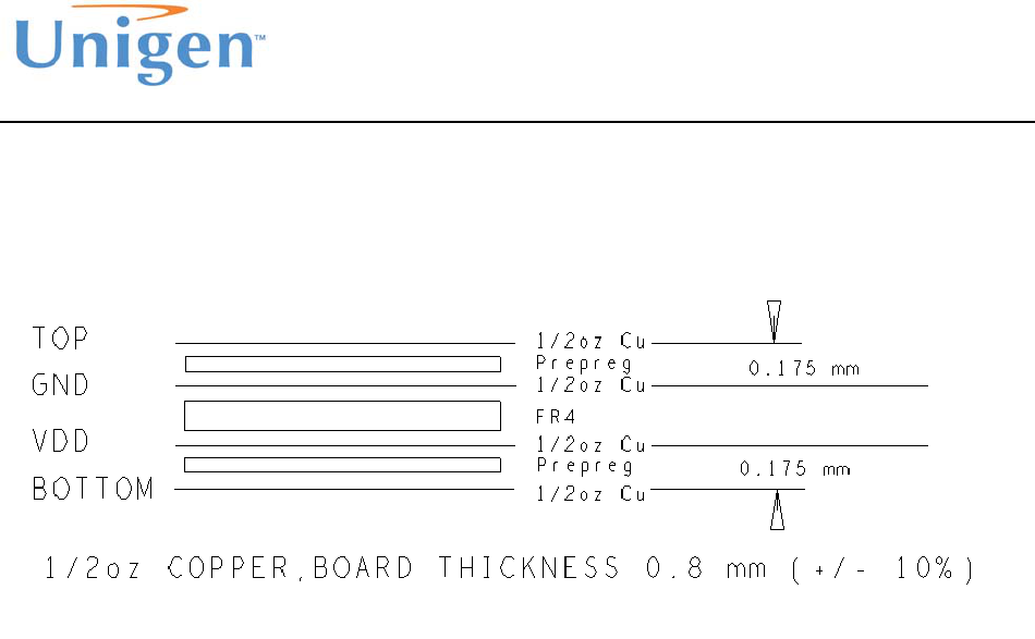
Figure15:NEMO2EvaluationMicrostripPCBStackUPDetails
Microstrip Ground Reference
The Microstrip will have a ground reference on the adjacent inner layer and top
(same) layer as the Microstrip. The Nemo2 reference evaluation board has an
adjacent ground plane inner layer below the Microstrip. The top layer has a ground
reference to the Microstrip as well. The spacing between the top ground references
is crucial and should be at least 3x the width of the Microstrip. The Nemo2
Evaluation board uses 1mm spacing from the Microstrip to the top layer ground
reference.
Solutions for a Real Time World NEMO2 Design Guidelines
Applicationnote
Figure16:NEMO2MicrostripGroundReference
A grid of through hole vias are used to join the top layer ground to the adjacent
inner layer ground plane. This is known as “stitching”. The integrator should use as
much stitching as possible.
Figure17:NEMO2GroundingTechnique,GroundStitchingandAdjacentGroundLayer
Solutions for a Real Time World NEMO2 Design Guidelines
Applicationnote
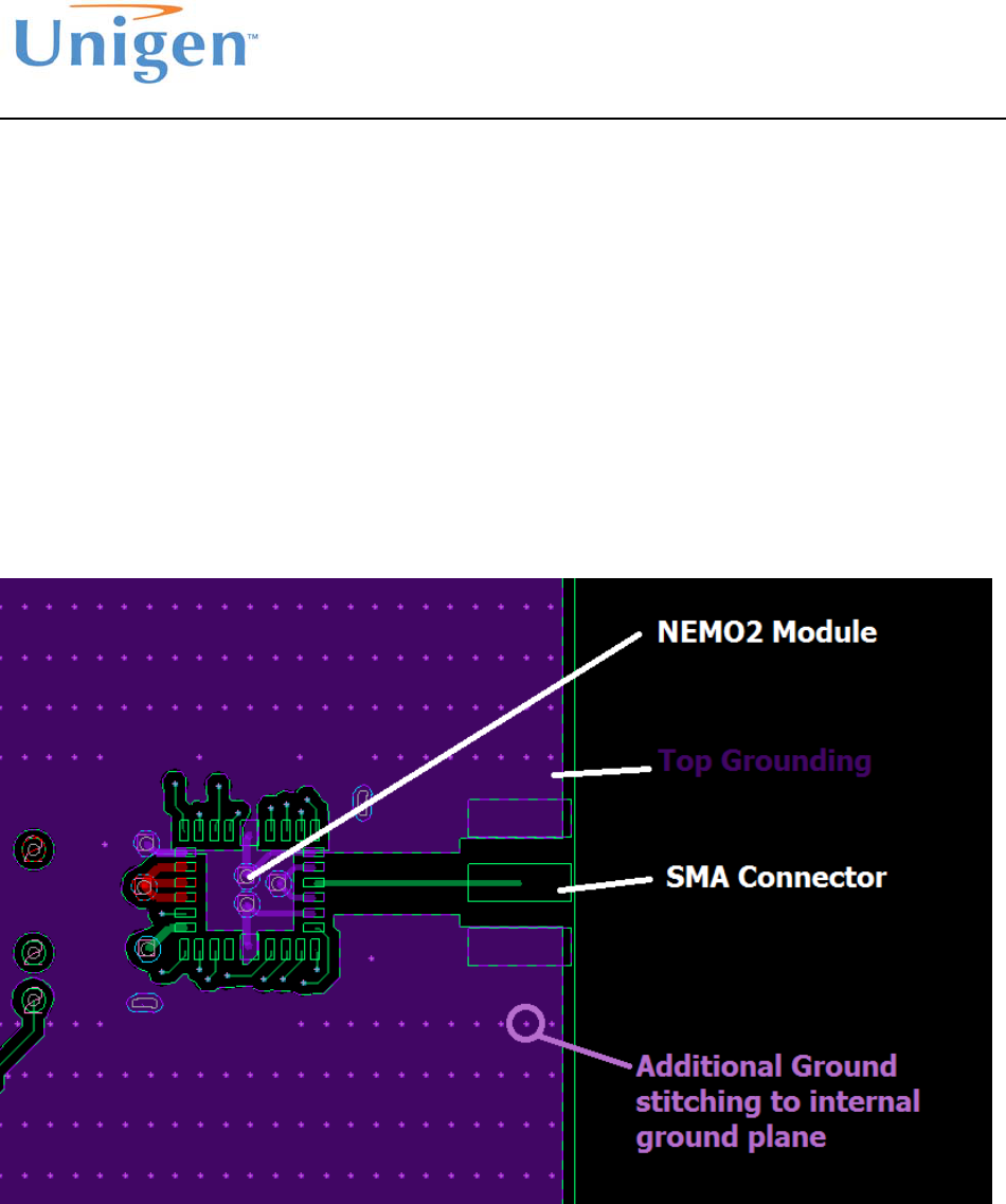
External grounding
External grounding and care is the integrators responsibility with the Nemo2 module for
functionality and RF integration with an antenna or antenna connector. A solid ground
reference is needed in particular to the Rf signal path to the terminating component
such as an antenna or antenna connector.
The Nemo2 evaluation board with a SMA connector and the SMA di-pole antenna took
great consideration of the RF path and its reference to ground. See below on the
layout of the top layer where the RF path resides and ground fill as a reference to the
RF signal.
Figure18:GroundingConsiderations
Solutions for a Real Time World NEMO2 Design Guidelines
Applicationnote
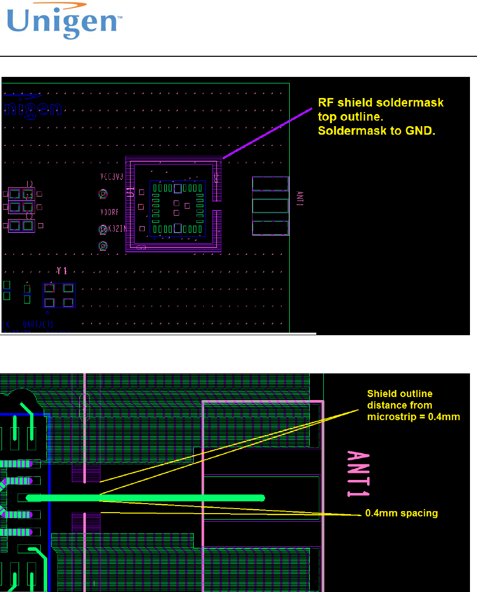
RF Shielding
The NEMO2 module is not shipped with an RF shield. In order to comply with
modular approvals, the integrator must shield the circuitry around the NEMO2
module on the integrators board. The shield must be grounded and shall have an
opening for the microstrip transmission line.
NEMO2 has received Limited Modular Approval due to the absence of a
shield and each OEM will be required to have Radiated Emissions
measured to ensure compliance.
There is an outline on the NEMO2 evaluation board for a metal shield. Below are
dimensions of the shield for the NEMO2 evaluation board. The shield is keyed for
placement with the PCB and shield outline also reflecting the keyed holes. The
details are provided in the NEMO2 evaluation board GERBERS. The gap spacing with
the microstrip is also illustrated below.
Figure19:NEMO2EvaluationBoardExampleShield
Solutions for a Real Time World NEMO2 Design Guidelines
Applicationnote
Figure20:NEMO2EvaluationBoardTopSoldermaskRFShieldOutline
Figure21:NEMO2EvaluationBoardRFShieldMicrostripgapspacing

Solutions for a Real Time World NEMO2 Design Guidelines
Applicationnote
Support Contact
ForanyinquiriesonthedesignandsupportofNemo2,pleasecontactsales@unigen.com
EndofDocument