Universal Scientific MESSI-V LTE Module User Manual UNA
Universal Scientific Industrial Co., Ltd. LTE Module UNA
Contents
- 1. User manual
- 2. User Manual
- 3. Manual compliance statement
User Manual
1/13 Rev1.2
MESSI-V M2 I/O APPLICATION
4G LTE Module
(NGFF type)
Doc. Title
MESSI-V M2 I/O APPLICATION
Originator
David Tsui
Concurrence
Achau Lee
Approved by
Version
Date
2013/08/08
2/13 Rev1.2
Revision History
Rev
Draft/Changes
Date
1.0
First version released (DVT phase)
2013/01/10
3/13 Rev1.2
Introduction:
MESSI-V M2 is an advanced and compact NGFF board / module which supports
LTE category 3 (CAT-3) throughputs. MESSI-V M2 supports for UART, USB2.0,
USIM and antenna interface. The details of I/O interfaces are described in the
sections as followings:
UART Interface
USB2.0 Interface
USIM Interface
Power Input
JTAG & Reset
GPIO
Antenna Interface
Others
4/13 Rev1.2
1. UART Interface
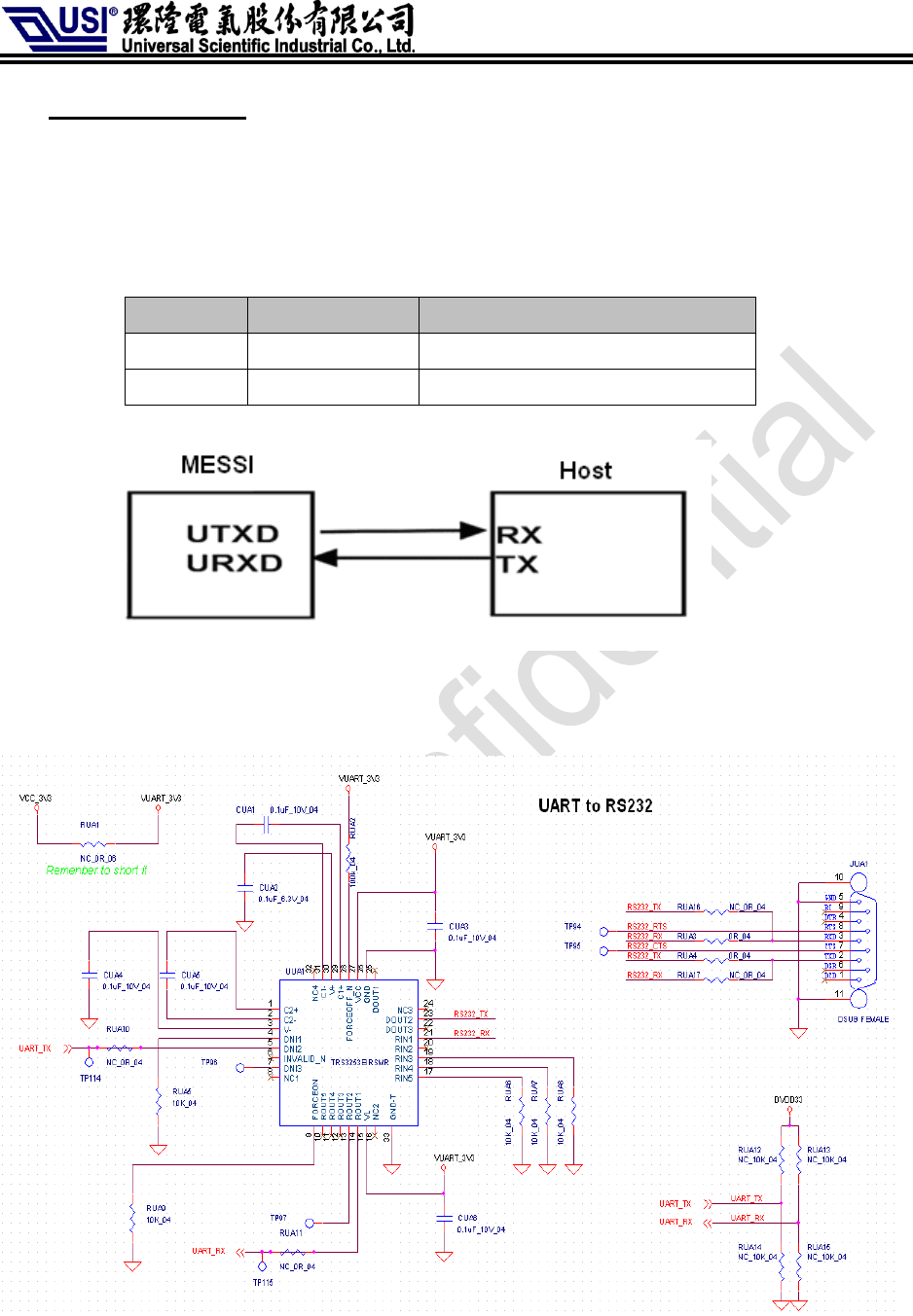
MESSI-V M2 board supports one UART port for debugging and downloading. The baud
rate speed is up to 115200bps. Signal level is 3.3V. If MESSI-V M2 module goes
through standard RS-232 interface to connect with PC, It is recommended to use TI
TRS3253EIRSMR for best baud rate to catch log file and download boot loader setting.
Pin NO.
Pin name
Description
62
UART_RX
UART receive input
64
UART_TX
UART transmit output
Figure1-1: UART block diagram.
Figure1-2: RS-232 connection
5/13 Rev1.2
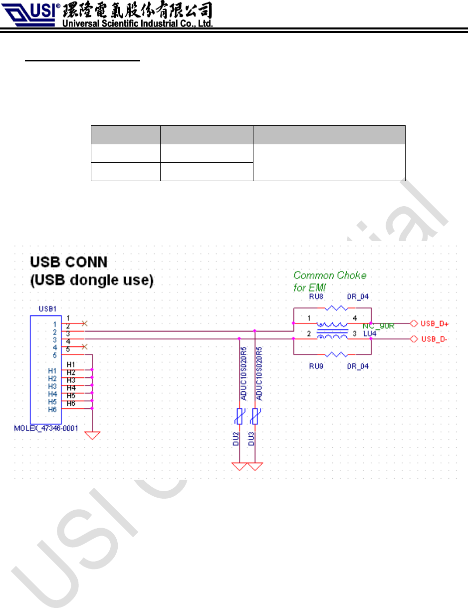
2. USB 2.0 Interface
The USB interface is compliant with Version 2.0 of the USB standard for high speed
operation. The reference circuit is showing in Figure2-1as following.
Pin NO.
Pin name
Description
7
USB_D+
Universal Serial BUS
9
USB_D-
Figure2-1: USB connection
6/13 Rev1.2
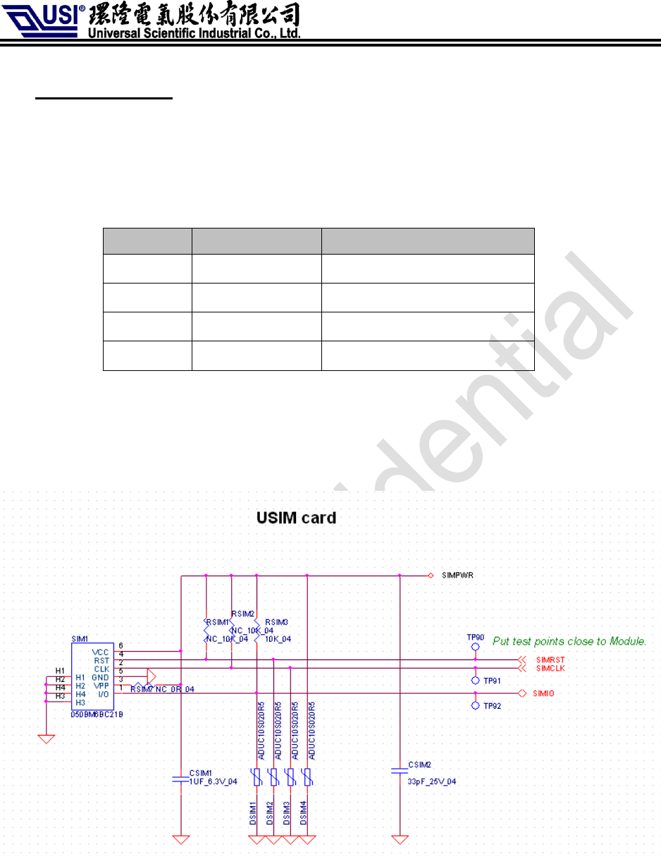
3. USIM interface
The USIM pins provide the connections necessary to interface to a USIM socket located
on the host device. Voltage levels over this interface comply with 3GPP standards.
MSEEI module outputs a SIMPWR power rail 1.8V and 3V.
Pin NO.
Pin name
Description
36
SIMPWR
1.8V/3V output to SIM card.
34
SIMIO
SIM data IO
32
SIMCLK
SIM clock
30
SIMRST
SIM reset
The reference circuit is showing in Figure3-1as following.
Figure3-1: USIM card connection
7/13 Rev1.2
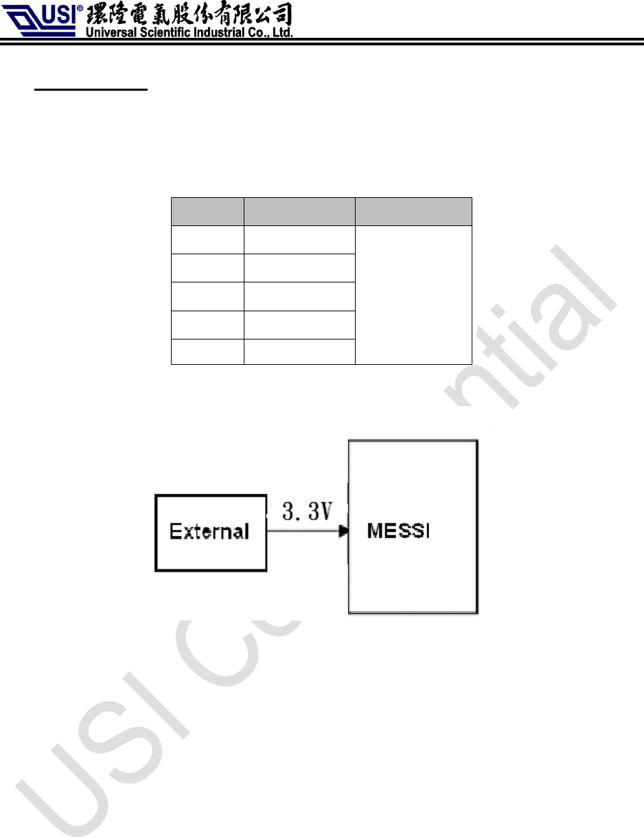
4. Power Input
MESSI-V M2 power input pin is VBAT. The power input range is from 3.4V to 5V with
USB, external power or Battery. Figure 4-1 shows external power source to MESSI
module.
Pin NO.
Pin name
Description
2
3.3V
Power input
4
3.3V
70
3.3V
72
3.3V
74
3.3V
Figure4-1: External power for MESSI-V M2 board.
8/13 Rev1.2
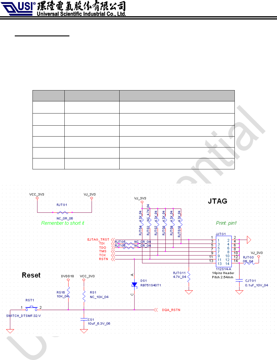
5. JTAG & Reset
Emulation JTAG is used to debug and run SW on embedded MIPS processors.
MESSI has a single Reset input (RSTN). This signal should be connected and driven by
the power management unit or the host application processor, depending on the usage
scenario.
Pin NO.
Pin name
Description
42
TCK
Clock
43
TMS
Test Mode
47
TDI
Input Data
49
TDO
Output Data
53
EJTAG_TRST
EJTAG Reset
67
TRST
MESSI Reset Input(1.8V)
Figure 6-1: JTAG connection
9/13 Rev1.2
6. GPIOs
MESSI-V M2 has various software-controlled general purpose IO (GPIO) pins which are
listed below. The user can use these GPIOs for any general purpose their design calls for.
If the GPIO is not in use, it is recommended to leave the pin as floating.
Pin NO.
Pin name
Description
8
GPIO4
3.3V General Purpose I/O
35
GPIO20
1.8V General Purpose I/O
31
GPIO19
1.8V General Purpose I/O
29
GPIO18
1.8V General Purpose I/O
20
GPIO11
1.8V General Purpose I/O
22
GPIO10
1.8V General Purpose I/O
24
GPIO9
1.8V General Purpose I/O
26
GPIO8
1.8V General Purpose I/O
28
GPIO12
1.8V General Purpose I/O
40
GPIO13
1.8V General Purpose I/O
42
GPIO14
1.8V General Purpose I/O
44
GPIO15
1.8V General Purpose I/O
46
GPIO16
1.8V General Purpose I/O
10/13 Rev1.2
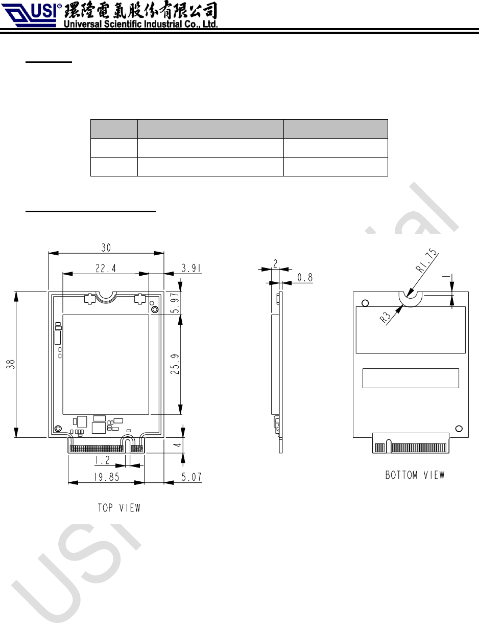
7. Antenna Interface
MESSI-V M2 support MIMO antenna. The reference RF cable SPEC is down below.
Pin NO.
Pin name
Description
ANT 1
RXTX
RF Transmission and RF receive chain
ANT 2
RXONLY
RF receive chain
Figure 8-1: MIMO antenna connection
11/13 Rev1.2
8. Others
The following Pins are reserved for future update. The user can leave these pin as
floating.
Pin NO.
Pin name
Description
23
PMU SLEEP/PWR_REQ
Reserved
66
SCR_DTCT
Reserved
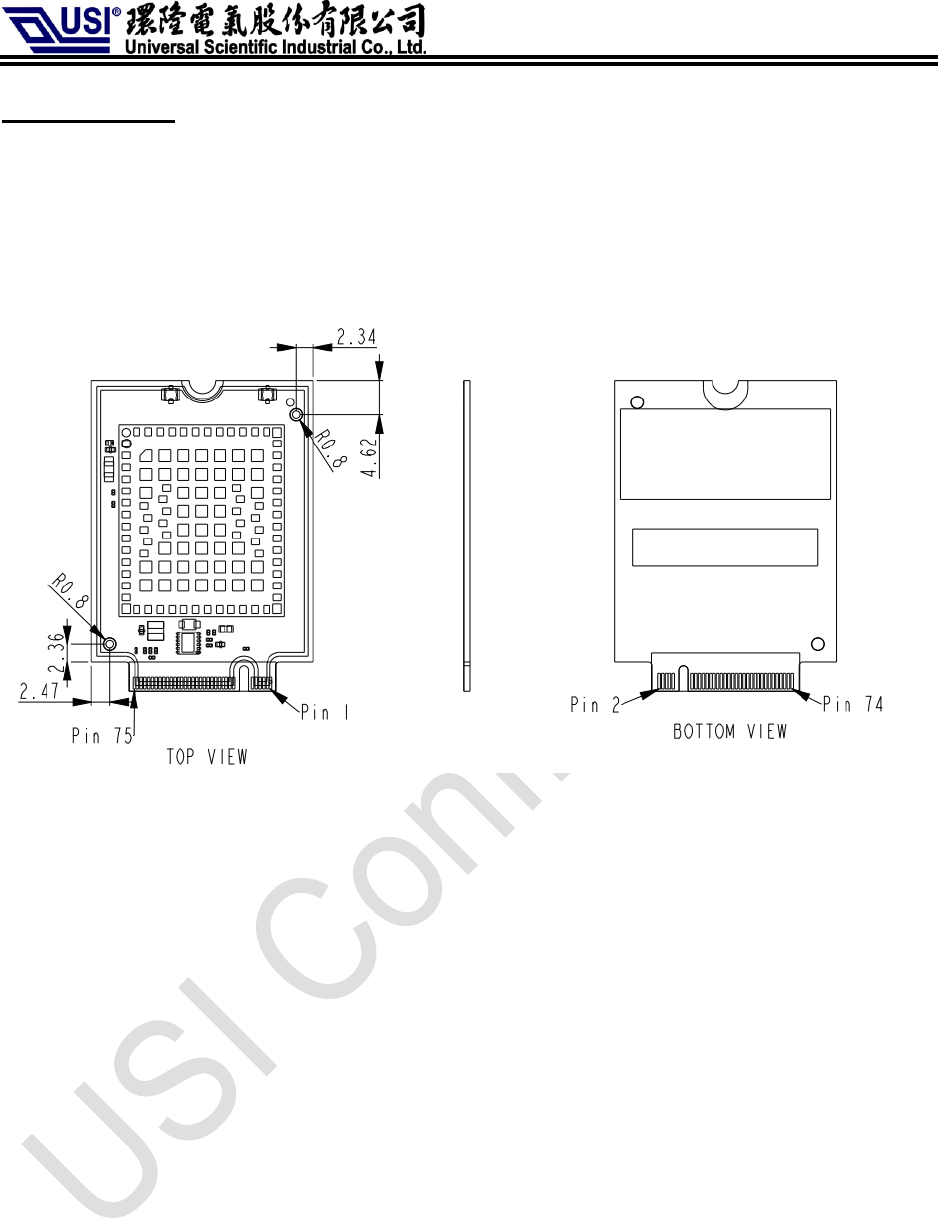
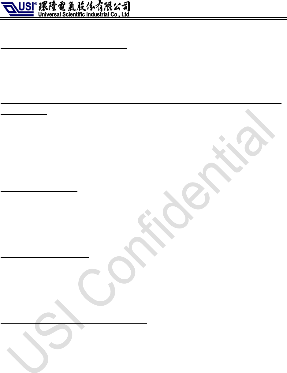
9. Mechanical Outline
Figure9-1: Messi-V M2 Mechanical

12/13 Rev1.2
Federal Communication Commission Interference Statement
This device complies with Part 15 of the FCC Rules. Operation is subject to the following
two conditions: (1) This device may not cause harmful interference, and (2) this device
must accept any interference received, including interference that may cause undesired
operation.
This equipment has been tested and found to comply with the limits for a Class B digital
device, pursuant to Part 15 of the FCC Rules. These limits are designed to provide
reasonable protection against harmful interference in a residential installation. This
equipment generates, uses and can radiate radio frequency energy and, if not installed
and used in accordance with the instructions, may cause harmful interference to radio
communications. However, there is no guarantee that interference will not occur in a
particular installation. If this equipment does cause harmful interference to radio or
television reception, which can be determined by turning the equipment off and on, the
user is encouraged to try to correct the interference by one of the following measures:
- Reorient or relocate the receiving antenna.
- Increase the separation between the equipment and receiver.
- Connect the equipment into an outlet on a circuit different from that
to which the receiver is connected.
- Consult the dealer or an experienced radio/TV technician for help.
FCC Caution: Any changes or modifications not expressly approved by the party
responsible for compliance could void the user's authority to operate this equipment.
This transmitter must not be co-located or operating in conjunction with any other
antenna or transmitter.
13/13 Rev1.2
Radiation Exposure Statement:
This equipment complies with FCC radiation exposure limits set forth for an uncontrolled
environment. This equipment should be installed and operated with minimum distance
20cm between the radiator & your body.
This device is intended only for OEM integrators under the following
conditions:
1) The antenna must be installed such that 20 cm is maintained between the antenna
and users, and
2) The transmitter module may not be co-located with any other transmitter or
antenna.
IMPORTANT NOTE: In the event that these conditions can not be met (for example
certain laptop configurations or co-location with another transmitter), then the FCC
authorization is no longer considered valid and the FCC ID can not be used on the final
product. In these circumstances, the OEM integrator will be responsible for re-evaluating
the end product (including the transmitter) and obtaining a separate FCC authorization.
End Product Labeling
This transmitter module is authorized only for use in device where the antenna may be
installed such that 20 cm may be maintained between the antenna and users. The final
end product must be labeled in a visible area with the following: “Contains FCC ID:
IXMMESSI-V”. The grantee's FCC ID can be used only when all FCC compliance
requirements are met.
Manual Information To the End User
The OEM integrator has to be aware not to provide information to the end user regarding
how to install or remove this RF module in the user’s manual of the end product which
integrates this module.
The end user manual shall include all required regulatory information/warning as show in
this manual.