Universal Scientific WM-BB-AG-01 801.11b + Bluetooth Module User Manual WM BB AG 01 2 4 2004 02 23
Universal Scientific Industrial Co., Ltd. 801.11b + Bluetooth Module WM BB AG 01 2 4 2004 02 23
Users Manual Revision 2
Federal Communication Commission Interference Statement
This equipment has been tested and found to comply with the limits for a Class B digital device,
pursuant to Part 15 of the FCC Rules. These limits are designed to provide reasonable
protection against harmful interference in a residential installation. This equipment generates,
uses and can radiate radio frequency energy and, if not installed and used in accordance with
the instructions, may cause harmful interference to radio communications. However, there is no
guarantee that interference will not occur in a particular installation. If this equipment does cause
harmful interference to radio or television reception, which can be determined by turning the
equipment off and on, the user is encouraged to try to correct the interference by one of the
following measures:
- Reorient or relocate the receiving antenna.
- Increase the separation between the equipment and receiver.
- Connect the equipment into an outlet on a circuit different from that to which the receiver is
connected.
- Consult the dealer or an experienced radio/TV technician for help.
FCC Caution: To assure continued compliance, (example - use only shielded interface cables
when connecting to computer or peripheral devices) any changes or modifications not expressly
approved by the party responsible for compliance could void the user's authority to operate this
equipment.
This device complies with Part 15 of the FCC Rules. Operation is subject to the following two
conditions: (1) This device may not cause harmful interference, and (2) this device must accept
any interference received, including interference that may cause undesired operation.
This device is intended only for OEM Integrators. The OEM integrator should be
aware of the following important issues.
Labeling of the End Product
The end product integrate this module has to be clearly identified on the label that this
end product contain an FCC approved RF module. The format of such statement
could containTx FCC ID: IXMWM-BB-AG-01 or similar.
Integration Note
a) This module is authorized under limited module approval specified to mobile host
equipment. So, the antenna must be installed such that 20cm is maintained
between the antenna and users.
b) The transmitter module may not be co-located with any other transmitter or
antenna.
As long as the 2 conditions above are met, further transmitter testing will not be
required. However, the OEM integrator is still responsible for testing their
end-product for any additional compliance requirements required with this module
installed (for example, digital device emission, PC peripheral requirements, etc.)
IMPORTANT NOTE:
In the event that these conditions can not be met (for example certain laptop
configurations, general purpose PCMCIA or similar cards, or co-location with another
transmitter), then the FCC authorization is no longer considered valid and the FCC ID
can not be used on the final product (including the transmitter) and obtaining a
separate FCC authorization.
could be " Contains Transmitter with FCC ID: IXMWM-BB-AG-01" or similar.
All rights are reserved by USI. No part of this technical document can be reproduced in any form without permission of USI.
1
Features
l Small size suitable for low volume
system integration.
l Low power consumption, extend
battery life.
l 2.412 – 2.484 GHz frequency band.
l Support hardware signaling
l Easy for integration into mobile and
handheld device with flexible system
configuration and antenna design.
Data Sheet
Feb. 2004, Rev 2.4
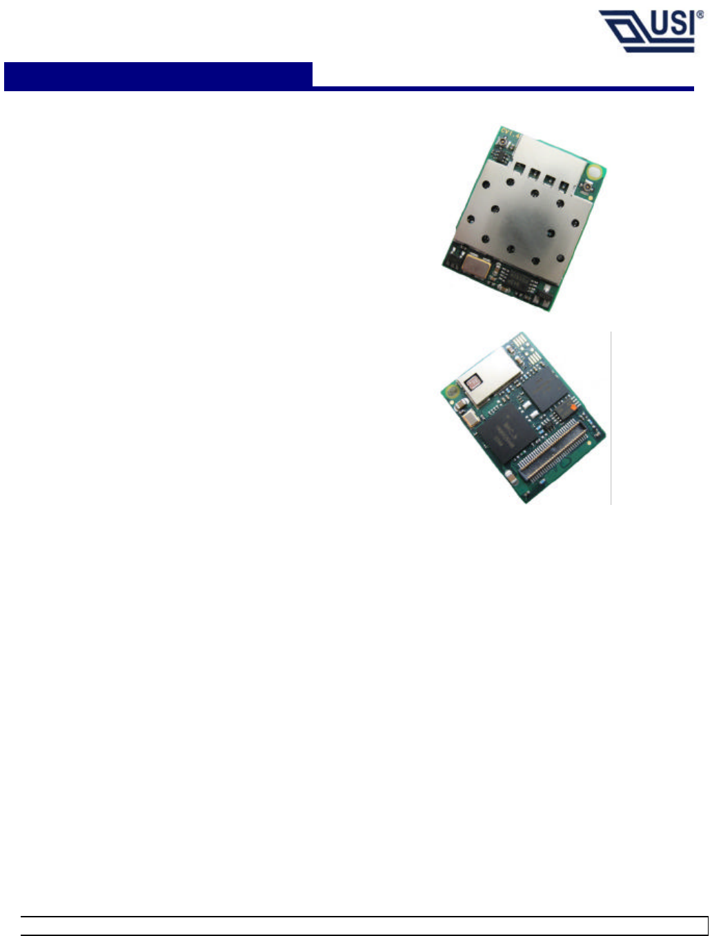
802.11b+Bluetooth COMBO SiP Module
WM
-
BB
-
AG
-
01
Introduction
The USI 802.11 Wireless SiP module WM-BB-AG-
01 which refers as “COMBO SiP module” is a full
small size module that provides full function of
802.11b and Bluetooth class 2 on a 22*29 mm tiny
module via 60 pins board to board connector.
This multi- functionality and board to board physical
interface provide system users the maximum
flexibility including system feature and system
integration.
WM-BB-AG-01 is approved as one of USI
embedded Wi-Fi module product lines. There are
two product variants of WM-BB-AG-01 by de-
populating either 802.11b or Bluetooth to be a
single module which provided better cost-
feature on
system with single design-in effort.
The small size design (22*29*3.5 mm), low power
consumption (Tx 330 mA) and excellent radio
performance make it the best solution which is
suitable for OEM customers who require embedded
802.11b Wi-Fi plus Bluetooth features, such as,
wireless PDA, barcode scanner, mini-printer, VoIP
phone etc.
For the hardware features, Agere 802.11 chipset
solution is adopted for 802.11b, and CSR BlueCore
02-ROM for Bluetooth. Two antenna connectors
provide antenna connectivity for each function.
In additional to the classic radio design, physical
signaling between Bluetooth and 802.11b functional
block provides the best performance when
Bluetooth and 802.11b function at the same time.
For the software and driver development, USI
provides extensive technical document and
reference software code for system integration.
Hardware evaluation kit and development utility will
be released base on listed OS and processors to
OEM customers under agreement for development.
www.usi.com.tw
802.11 b + Bluetooth COMBO SiP Module v 2.4
All rights are reserved by USI. No part of this technical document can be reproduced in any form without permission of USI.
2
OEM Deliverables
• WM-BB-AG-01 with packing
•
Test Platform includes application (PDA ), software utilities which support
customers for integration, performance tests, and homologation.
Temperature and Humidity .
Operating Temperature 0° to 60° Celsius
Non Operating Temperature -10° to 70° Celsius
Humidity Range 20% to 90%( Non-condensing, relative)
Voltage and Current
Power supply for the WM-BB-AG-01 will be provided by the host via the board to board
connector.
Voltage
Operating Voltage 3.3 Volt (Typ.), Max 3.6V, Min 3.15V
Voltage Ripple +/- 2%(Max value not exceeding operating voltage)
Current (Typical)
Continuous Transmit 340 mA (Both 802.11 and BT in transmit mode)
Continuous Receive 230 mA (Both 802.11 and BT in receive mode)
Sleep Mode 16 mA (Both 802.11 and BT in sleep mode)
Wireless Specification
The WM-BB-AG-01 complies with the following features and standards;
Features Description
WLAN Standards IEEE 802 Part 11b (802.11b)
Bluetooth BluetoothTM 1.1
Antenna Connector Two antenna connectors support 802.11b and BT one for each.
Coexistence Hardware signaling
Frequency Band 2.402– 2.484 GHz
LED Specification
The WM-BB-AG-01 have 2 LED’s (output) via 60 pins connector for feedback to the user on
the current WLAN and Bluetooth activity state with individual LED. The signaling will reflect
status / activity as described in the table below. The signal is provided via the board to board
connector with the following pin assignment.
802.11 b + Bluetooth COMBO SiP Module v 2.4
All rights are reserved by USI. No part of this technical document can be reproduced in any form without permission of USI.
3
Pin No Pin description Function description
42 WLAN_LED Link Activity of Wireless LAN
55 BT_LED Link Activity of Bluetooth
The LED code and related status of the wireless module are listed below:
WLAN_LED
BT_LED Cycle Time
Radio on and no activity (when
device is in scan mode) Blinking Blinking LED on time: 200ms
LED off time: 2000ms
Radio on and activity in each radio Blinking Blinking LED on time: 100ms
LED off time: 400ms
Radio off Off Off
802.11b Radio Specification
The radio specification is compliant with the SPEC of 802.11b.
Features Description
Frequency Band 2.412 – 2.484 GHz (2.4 GHz ISM Band)
Number of Selectable Channels 14 channels
Modulation DSSS (Direct Sequence Spread Spectrum),
DBPSK, DQPSK, CCK
Supported Rates 1,2, 5.5 and 11 Mbps
Maximum Receive Level - 10 dBm (with PER < 8%)
Output Power 13.5 dBm +-1.0 dB
Antenna Connector One Hirose W.FL –R –SMT(10) RF connector
802.11b Radio Characteristics
Receive Sensitivity Data Rates
- 82 dBm 11 Mbps
- 85 dBm 5.5 Mbps
- 88 dBm 2.0 Mbps
- 91 dBm 1.0 Mbps
* Under normal operation at room temperature.

802.11 b + Bluetooth COMBO SiP Module v 2.4
All rights are reserved by USI. No part of this technical document can be reproduced in any form without permission of USI.
4
Bluetooth Radio Specification
The Radio specification is compliant with the Bluetooth v1.1 class 2 specification
Features Description
Frequency Band 2.402 – 2.484 GHz
Number of Channels 79 channels
Modulation FHSS (Frequency Hopping Spread Spectrum)
Antenna Connector One Hirose W.FL –R –SMT(10) RF connector
Bluetooth Radio Characteristics
Features Description
Maximum Receive Level 0 dBm(Min) , 3dBm (typical)
Output Power 3 dBm (typical) , 6 dbm (Max)
Sensitivity -81 dbm @ 0.1% BER @ 25 ° Celsius ( Typical )
Compatibility and Interoperability
Wi-Fi Logo
Wi-Fi certification is limited and dependent on the capability and application of the host system.
WHQL Compliance
N/A
BQB Compliance
WM-BB-AG-01 is verified and proved BQB certificated.
802.11 b + Bluetooth COMBO SiP Module v 2.4
All rights are reserved by USI. No part of this technical document can be reproduced in any form without permission of USI.
5
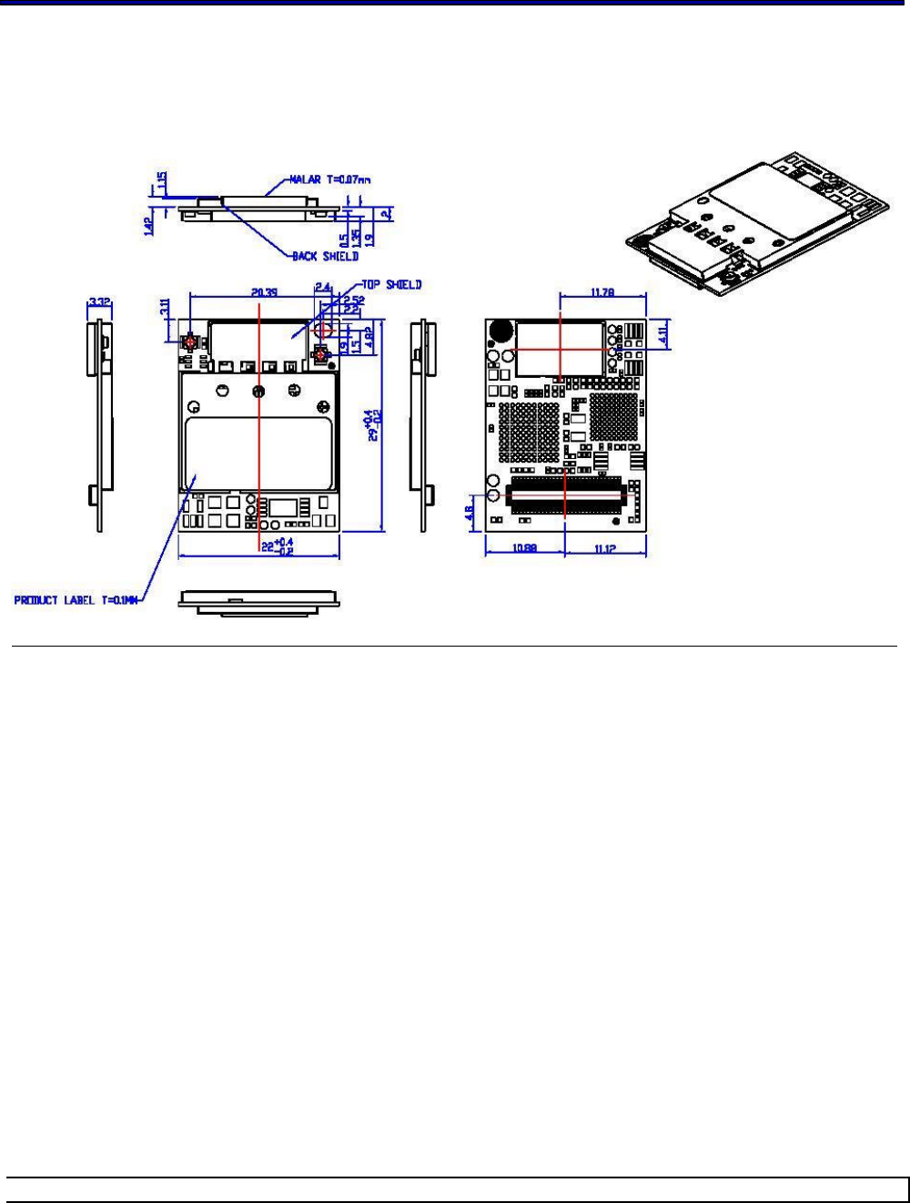
Mechanical Dimensions
Dimensions: 22 mm x 29 mm x 3.5 mm (excluding RF cable assembly)
Shock and Vibration
The WM-BB-AG-01 has been developed for incorporated into other devices. No shock and
vibration tests for this module has been performed.
Configuration
Users don’t need to configure it. The CIS and MAC Address and Bluetooth ID address will be
loaded during production of the WM-BB-AG-01 (RTS).
Security
WEP 64/128 bits.
802.11 b + Bluetooth COMBO SiP Module v 2.4
All rights are reserved by USI. No part of this technical document can be reproduced in any form without permission of USI.
6
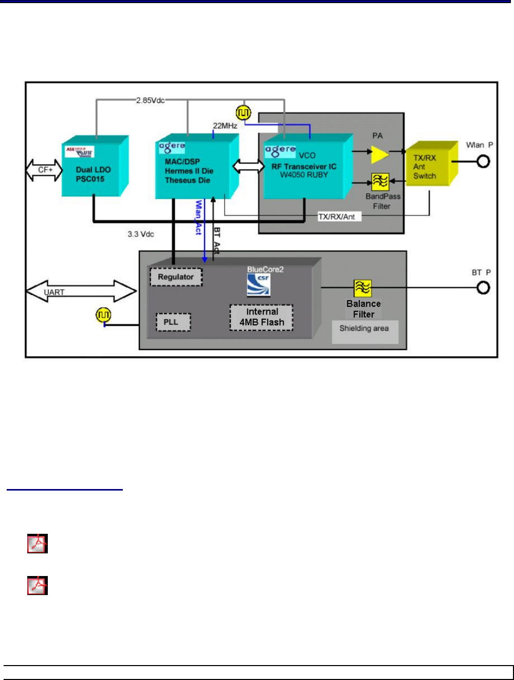
Functional Block Diagram
A simplified block diagram of the WM-BB-AG-01 is depicted in the picture below.
Host Interface
The host interface will be compatible with CompactFlash (PCMCIA) standard, 16 bit I/O bus.
Signals which are not used won’t be routed to the physical interface (connector). The host
interface of SiP Combo is compliant with UART interface.
For the connector, high reliability connectors will be used.
On Board connector
Molex SD53794-0608 [Socket, 60 pins, with positioning protection, stack height which is
able to support 1.5 mm.
sd537941.pdf
sd537942.pdf

802.11 b + Bluetooth COMBO SiP Module v 2.4
All rights are reserved by USI. No part of this technical document can be reproduced in any form without permission of USI.
7
Host System:
Molex SD54037-0607 [Header, 60 pins, with positioning protection, stack height 1.5mm]
sd540371.pdf
Pin Definition
[ …] means optional function of the pin.
PD : Signal pull down internally in the chip by 20K ohm register while initialization.
PU : Signal pull up internally in the chip by 20K ohm register while initialization.
WPD: Signal pull down internally in the chip by 1Mohm register during initialization
WPU: Signal pull up internally in the chip by 1Mohm register during initialization
5VT: 5 Volt tolerance pin
xxx_B : Signal pins end with _B are “active Low”
Pin
Number
Definition
Draft Description Type
WM-BB-
AG-01
CF+ interface
1 GND GND GND
2 D03 HD3 Data Input/Output line constitute a bi-directional
bus. HD[15:0] are used to access the MODULE
MAC Host Interface register
O, PD, 5VT, 4mA
Databus
3 D04 HD4 Data Input/Output line constitute a bi-directional
bus. HD[15:0] are used to access the MODULE
MAC Host Interface register
O, PD, 5VT, 4mA
Databus
4 D05 HD5 Data Input/Output line constitute a bi-directional
bus. HD[15:0] are used to access the MODULE
MAC Host Interface register
IO, PD, 5VT, 4mA
Databus
5 D06 HD6 Data Input/Output line constitute a bi-directional
bus. HD[15:0] are used to access the MODULE
MAC Host Interface register
IO, PD, 5VT, 4mA
6 D07 HD7 Data Input/Output line constitute a bi-directional
bus. HD[15:0] are used to access the MODULE
MAC Host Interface register
IO, PD, 5VT, 4mA
7 -CE_1 HCE1_B Card Enable1 is driven by the host system and is
used as select strobe in both I/O and memory
mode. Enables even numbered address bytes.
Input, PU, 5VT
8 A10 A10 ADDRESS BUS lines driven by the host system
which enables addressing of 0.5K address range
within HERMES II. The pin is open in B2B module.
N/A
9 -OE HOE_B OUTPUT ENABLE is driven by the host during a
memory Read Access. Input, PU,5VT
10 A09 HA9 ADDRESS BUS lines driven by the host system
which enables addressing of 0.5K address range
within HERMES II. This address range is mainly
used for accessing the CIS in Memory Mode. Signal
HA0 is not used in word access mode.
Input, PD,5VT

802.11 b + Bluetooth COMBO SiP Module v 2.4
All rights are reserved by USI. No part of this technical document can be reproduced in any form without permission of USI.
8
11 A08 HA8 ADDRESS BUS lines driven by the host system
which enables addressing of 0.5K address range
within HERMES II. This address range is mainly
used for accessing the CIS in Memory Mode. Signal
HA0 is not used in word access mode.
Input, PD,5VT
12 A07 HA7 ADDRESS BUS lines driven by the host system
which enables addressing of 0.5K address range
within HERMES II. This address range is mainly
used for accessing the CIS in Memory Mode. Signal
HA0 is not used in word access mode.
Input, PD,5VT
13 VCC VCC_WLAN Power, 3.3V_WLAN Input
14 A06 HA6 ADDRESS BUS lines driven by the host system
which enables addressing of 0.5K address range
within HERMES II. This address range is mainly
used for accessing the CIS in Memory Mode. Signal
HA0 is not used in word access mode.
Input, PD, 5VT
15 A05 HA5 ADDRESS BUS lines driven by the host system
which enables addressing of 0.5K address range
within HERMES II. This address range is mainly
used for accessing the CIS in Memory Mode. Signal
HA0 is not used in word access mode.
Input, PD, 5VT
16 A04 HA4 ADDRESS BUS lines driven by the host system
which enables addressing of 0.5K address range
within HERMES II. This address range is mainly
used for accessing the CIS in Memory Mode. Signal
HA0 is not used in word access mode.
Input, PD, 5VT
17 A03 HA3 ADDRESS BUS lines driven by the host system
which enables addressing of 0.5K address range
within HERMES II . This address range is mainly
used for accessing the CIS in Memory Mode. Signal
HA0 is not used in word access mode.
Input, PD, 5VT
18 A02 HA2 ADDRESS BUS lines driven by the host system
which enables addressing of 0.5K address range
within HERMES II. This address range is mainly
used for accessing the CIS in Memory Mode. Signal
HA0 is not used in word access mode.
Input, PD, 5VT
19 A01 HA1 ADDRESS BUS lines driven by the host system
which enables addressing of 0.5K address range
within HERMES II. This address range is mainly
used for accessing the CIS in Memory Mode. Signal
HA0 is not used in word access mode.
Input, PD, 5VT
20 A00 HA0 ADDRESS BUS lines driven by the host system
which enables addressing of 0.5K address range
within HERMES II. This address range is mainly
used for accessing the CIS in Memory Mode. Signal
HA0 is not used in word access mode.
Input, PD, 5VT
21 D00 HD0 Data Input/Output line constitute a bi-directional
bus. HD[15:0] are used to access the MODULE
MAC Host Interface register
IO, PD, 5VT, 4mA
22 D01 HD1 Data Input/Output line constitute a bi-directional
bus. HD[15:0] are used to access the MODULE
MAC Host Interface register
IO, PD, 5VT, 4mA
23 D02 HD2
Data Input/Output line constitute a bi
-
directional
bus. HD[15:0] are used to access the MODULE
IO, PD, 5VT, 4mA

802.11 b + Bluetooth COMBO SiP Module v 2.4
All rights are reserved by USI. No part of this technical document can be reproduced in any form without permission of USI.
9
bus. HD[15:0] are used to access the MODULE
MAC Host Interface register
24 -IOIS16 HIOIS16_B Control signal to enable engineer testing mode Out, 6mA,5V T
25 -CD2 CD2 Normal operation, this pin is functionally for card
detection. Out, 6mA, 5VT.
26 N/A TXD_B UART CMOS output data line Output,WPU, 1µ
A
27 N/A RTS_B UART CMOS output signal, request to sent Output ,WPU, 1µ
A
28 N/A N/ A NA No connection
29 N/A VCC_WLAN Power_WLAN Input
30 GND GND
31 GND GND
32 D10 HD10 Data Input/Output line constitute a bi-directional
bus. HD[15:0] are used to access the MODULE
MAC Host Interface register
IO, PD, 5VT, 4mA
33 D09 HD9 Data Inp ut/Output line constitute a bi-directional
bus. HD[15:0] are used to access the MODULE
MAC Host Interface register
IO, PD, 5VT, 4mA
34 D08 HD8 Data Input/Output line constitute a bi-directional
bus. HD[15:0] are used to access the MODULE
MAC Host Interface register
IO, PD, 5VT, 4mA
35 -STSCHG HSTSCHG_B
STATUS CHANGE indication to the host. This
signal gets active when one of the bits in the PRR
or CSR registers are set
Output, 4mA
36 -SPKR N/A N/A No connection
37 -REG HREG_B ATTRIBUTE MEMORY SELECT is driven by the
host system and is used to access the Attribute
Memory
Input, PU, 5VT
38 -INPACK HINPACK_B INPUT ACKNOWLEDGE is driven by HERMES II.
Is asserted when the device is selected and the
device is responding to an I/O Read command.
Output, 2mA
39 -WAIT HWAIT_B HWAIT_B is driven by HERMES II and allows for
extending the memory or I/O cycle Output, 4mA
40 RESET HRESET Used to asynchronously reset the complete Module
Input, PU,5VT
41 -VS2 VS2_B Voltage sense signal Output , 5VT 4mA
42 N/A WLAN_LED_B
WLAN LED control signal, driven the LED
indicating the link status of WLAN Output, 4mA
43 N/A N/A Reserved pin No connection
44 IREQ
IREQ_B INTERRUPT REQUEST to the host. In Memory
mode this pin signifies RDY/BSY_typically used
during card initialization immediately after reset or
power on. Indicates to the host that the device is
not able to transfer data
Output, 4mA
45 -WE HWE_B WRITE ENABLE is driven by the host during a
memory Write Access Input, PU,5VT
46 -IOWR HIOWR_B
I/O Write Strobe is
driven by the host and is
asserted when the host wants to write to an on-
chip
I/O register
Input, PU,5VT
802.11 b + Bluetooth COMBO SiP Module v 2.4
All rights are reserved by USI. No part of this technical document can be reproduced in any form without permission of USI.
10
I/O register
47 -IORD HIORD_B I/O Read Strobe is driven by the host and is
asserted when the host wants to read from an on-
chip I/O register
Input, PU,5VT
48 -VS1 RF control RF CONTROL is driven by the host system and is
used to enable and disable the RF circuit block Output , 5VT
49 -CE2 HCE2_B CARD ENABLE2 is driven by the host system and
is used as select strobe in both I/O and memory
mode. Enables odd numbered address bytes
Input, PU,5VT
50 D15 HD15 Data Input/Output line constitute a bi-directional
bus. HD[15:0] are used to access the MODULE
MAC Host Interface register
IO, PD, 5VT, 4mA
51 D14 HD14 Data Input/Output line constitute a bi-directional
bus. HD[15:0] are used to access the MODULE
MAC Host Interface register
IO, PD, 5VT, 4mA
52 D13 HD13 Data Input/Output line constitute a bi-directional
bus. HD[15:0] are used to access the MODULE
MAC Host Interface register
IO, PD, 5VT, 4mA
53 D12 HD12 Data Input/Output line constitute a bi-directional
bus. HD[15:0] are used to access the MODULE
MAC Host Interface register
IO, PD, 5VT, 4mA
54 D11 HD11 Data Input/Output line constitute a bi-directional
bus. HD[15:0] are used to access the MODULE
MAC Host Interface register
IO, PD, 5VT, 4mA
55 N/A BT_LED_B BT LED control signal which drive the LED to
indicate the activity of Bluetooth Output 4mA
56 N/A RXD_B UART data line CMOS input signal Input, WPD, 1µA
57 N/A CTS_B UART clear to sent COMS input signal Input, WPD, 1µA
58 N/A N/A N/A N/A
59 VCC VCC_BT Power 3.3V_BT Input
60 GND GND
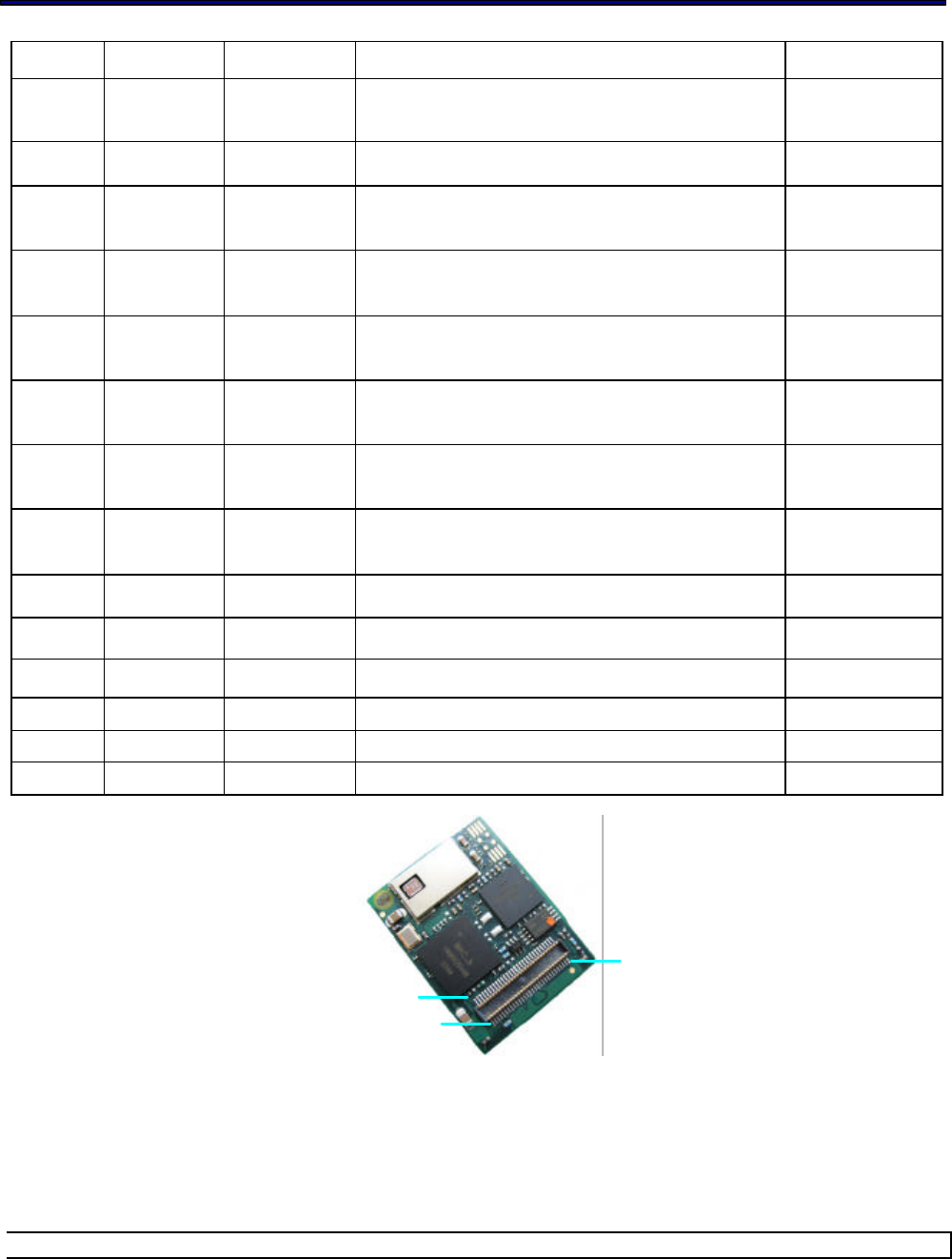
FIG 1: PIN 1 ASSIGNMENT AND INDICATION DRAWING
Pin 1
Pin 59
Pin 60

802.11 b + Bluetooth COMBO SiP Module v 2.4
All rights are reserved by USI. No part of this technical document can be reproduced in any form without permission of USI.
11
Antenna Interface
No antenna diversity supported on the 802.11b , neither BT on this COMBO Wireless
The output impedance of the cable is 50 Ohms.
Antenna Connector: Hirose W.FL-R-SMT (10)
Operating System Compatibility
Drivers are supported for the following OS:
• Windows CE 3.0/.NET
• Windows 98SE/2000/XP
Reliability
The WM-BB-AG-01 will guarantee a MTBF of 100,000 hours based on an ambient
temperature and workload of 2,920 hours. The workload is based on a unit working for 8 hours
per day, 365 days per year.
802.11 b + Bluetooth COMBO SiP Module v 2.4
All rights are reserved by USI. No part of this technical document can be reproduced in any form without permission of USI.
12
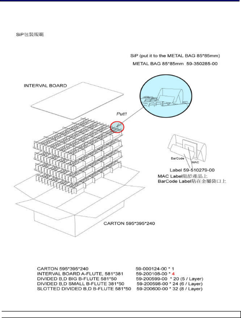
Packaging Design

802.11 b + Bluetooth COMBO SiP Module v 2.4
All rights are reserved by USI. No part of this technical document can be reproduced in any form without permission of USI.
13
For Additional information, please contact the following:
Universal Scientific Industrial Co., Ltd.
Headquarters
141, Lane 351, Taiping Road, Sec. 1, Tsao-Tuen , Taiwan,
Http://www.usi.com.tw
Tel: + 886-49-2350876, 2325876
Fax: +886-49-3439561, 2337360, 2351093
E-mail:usi@ms.usi.com.tw