VALEO Telematik und Akustik PNADB GSM/GPRS/UMTS/HSDPA/HSUPA Module with GPS and GLONASS User Manual
Peiker acustic GmbH & Co. KG GSM/GPRS/UMTS/HSDPA/HSUPA Module with GPS and GLONASS
User manual

________________________________________________________________________________________________________________________________________ Site 1
peiker acustic GmbH & Co. KG, Max-Planck-Straße 28-32, D-61381 Friedrichsdorf, Amtsgericht Bad Homburg HRA 1897
phG: peiker Verwaltungs GmbH, Vorsitzender der Geschäftsführung: Andreas Peiker, Geschäftsführer: Reinhard Kromer-von Baerle, Amtsgericht Bad Homburg HRB 1369
Vorsitzender des Aufsichtsrates: Dr. Helmut Rothenberger Ein Unternehmen der peiker Firmengruppe
NAD6200 Network Access Device
Datasheet, Rev. 1.3
september, 2013
PEIKER acustic Confidential and Proprietary
________________________________________________________________________________________________________________________________________ Site 2
peiker acustic GmbH & Co. KG, Max-Planck-Straße 28-32, D-61381 Friedrichsdorf, Amtsgericht Bad Homburg HRA 1897
phG: peiker Verwaltungs GmbH, Vorsitzender der Geschäftsführung: Andreas Peiker, Geschäftsführer: Reinhard Kromer-von Baerle, Amtsgericht Bad Homburg HRB 1369
Vorsitzender des Aufsichtsrates: Dr. Helmut Rothenberger Ein Unternehmen der peiker Firmengruppe
Revision History
Revision
Date
Chapter
Comment
1.0
13.5.2013
all
Release
1.1
17.7.2013
10
Insert chapter 10.2 Warning Statements
1.2
28.8.2013
10
Insert RF Exposure Warning and Notice
1.3
2.9.2013
10
Insert OEM responsibility to the FCC rules and regulations

________________________________________________________________________________________________________________________________________ Site 3
peiker acustic GmbH & Co. KG, Max-Planck-Straße 28-32, D-61381 Friedrichsdorf, Amtsgericht Bad Homburg HRA 1897
phG: peiker Verwaltungs GmbH, Vorsitzender der Geschäftsführung: Andreas Peiker, Geschäftsführer: Reinhard Kromer-von Baerle, Amtsgericht Bad Homburg HRB 1369
Vorsitzender des Aufsichtsrates: Dr. Helmut Rothenberger Ein Unternehmen der peiker Firmengruppe
Index of contents
Abstract .................................................................................................................................. 9
1. Introduction ................................................................................................................... 10
1.1. Scope ............................................................................................................................. 10
1.2. References ...................................................................................................................... 10
1.3. Audience ......................................................................................................................... 10
1.4. Contact information, support ............................................................................................ 10
2. Overview of the NAD6200 – Module .............................................................................. 11
2.1. Key features .................................................................................................................... 11
2.2. Product variants and Approvals ......................................................................................... 13
3. Overview HW – Part ....................................................................................................... 14
3.1. Block – Diagram .............................................................................................................. 14
3.2. Pin description of the board to board connector ................................................................. 15
3.3. HW – Features ................................................................................................................ 17
3.3.1. W-WAN connectivity .................................................................................................. 17
3.3.1.1. GSM/EDGE ......................................................................................................... 17
3.3.1.2. UMTS/WCDMA ................................................................................................... 17
3.3.1.3. GNSS ................................................................................................................. 18
3.3.2. Detailed Pin description ............................................................................................. 18
3.3.2.1. Power Supply ..................................................................................................... 18
3.3.2.2. KPD_Power ........................................................................................................ 19
3.3.2.3. RES_IN .............................................................................................................. 19
3.3.2.4. VREG_MSME ...................................................................................................... 20
3.3.2.5. SIM Card ........................................................................................................... 20
3.3.2.6. USB ................................................................................................................... 21
3.3.2.7. GPIOs ................................................................................................................ 22
3.3.2.8. UART ................................................................................................................. 24
3.3.2.9. I²C .................................................................................................................... 24
3.3.2.10. I²S ................................................................................................................... 25
3.3.2.11. GPS Pins ........................................................................................................... 26
3.3.3. Antenna ................................................................................................................... 26
3.3.3.1. Antenna connector ............................................................................................. 26

________________________________________________________________________________________________________________________________________ Site 4
peiker acustic GmbH & Co. KG, Max-Planck-Straße 28-32, D-61381 Friedrichsdorf, Amtsgericht Bad Homburg HRA 1897
phG: peiker Verwaltungs GmbH, Vorsitzender der Geschäftsführung: Andreas Peiker, Geschäftsführer: Reinhard Kromer-von Baerle, Amtsgericht Bad Homburg HRB 1369
Vorsitzender des Aufsichtsrates: Dr. Helmut Rothenberger Ein Unternehmen der peiker Firmengruppe
3.3.3.2. Antenna Switching .............................................................................................. 27
3.3.3.3. Antenna diagnostics ............................................................................................ 28
3.3.4. Chipset MDM6200 + PM8028 ..................................................................................... 28
3.3.4.1. PM8028 ............................................................................................................. 28
3.3.4.2. MDM6200 .......................................................................................................... 28
3.3.5. Memory .................................................................................................................... 29
4. Application software ...................................................................................................... 30
5. Antenna characteristics ................................................................................................. 31
5.1. Electrical characteristics for the Antenna ............................................................................ 31
5.2. Electrical characteristics for the Bands ............................................................................... 31
5.2.1. Frequencies .............................................................................................................. 31
5.2.2. Power Consumption, Call ........................................................................................... 32
6. Environmental Specification .......................................................................................... 34
6.1. General information ......................................................................................................... 34
6.2. Temperature Range ......................................................................................................... 34
7. Mechanical Specification ................................................................................................ 35
8. Safety Recommendations according to EN60950-1 ....................................................... 36
9. Evaluation Kit ................................................................................................................. 37
10. Appendix ........................................................................................................................ 39
10.1. AT Command list .......................................................................................................... 39
10.2. Warning Statements ..................................................................................................... 40

________________________________________________________________________________________________________________________________________ Site 5
peiker acustic GmbH & Co. KG, Max-Planck-Straße 28-32, D-61381 Friedrichsdorf, Amtsgericht Bad Homburg HRA 1897
phG: peiker Verwaltungs GmbH, Vorsitzender der Geschäftsführung: Andreas Peiker, Geschäftsführer: Reinhard Kromer-von Baerle, Amtsgericht Bad Homburg HRB 1369
Vorsitzender des Aufsichtsrates: Dr. Helmut Rothenberger Ein Unternehmen der peiker Firmengruppe
Index of figures
Figure 1: Block diagram of NAD6200 module ....................................................................... 14
Figure 2: board to board pin connector ................................................................................ 16
Figure 3: Mating connector .................................................................................................. 16
Figure 4: Pin description of GSBIs ........................................................................................ 23
Figure 5: Antenna connectors .............................................................................................. 26
Figure 6: FAKRA HF Single connector ................................................................................... 27
Figure 7: FAKRA HF Dual connector ..................................................................................... 27
Figure 8: Mechanical dimensions of the NAD6200 module ................................................... 35
Figure 9: Mechanical dimensions of the NAD6200 module (top view) ................................. 35
Figure 10: Evaluation Kit for NAD6200 module .................................................................... 37

________________________________________________________________________________________________________________________________________ Site 6
peiker acustic GmbH & Co. KG, Max-Planck-Straße 28-32, D-61381 Friedrichsdorf, Amtsgericht Bad Homburg HRA 1897
phG: peiker Verwaltungs GmbH, Vorsitzender der Geschäftsführung: Andreas Peiker, Geschäftsführer: Reinhard Kromer-von Baerle, Amtsgericht Bad Homburg HRB 1369
Vorsitzender des Aufsichtsrates: Dr. Helmut Rothenberger Ein Unternehmen der peiker Firmengruppe
Index of tables
Table 1: References .............................................................................................................. 10
Table 2: Key features of NAD6200 - Module ......................................................................... 11
Table 3: Product variants ..................................................................................................... 13
Table 4: Pin description of the board to board connector .................................................... 15
Table 5: Features of the GPS ................................................................................................ 18
Table 6: Characteristics of GLONASS .................................................................................... 18
Table 7: nominal values of the NAD6200 - module .............................................................. 19
Table 8: Electrical characteristics of KPD_Power ................................................................. 19
Table 9: Electrical characteristics of RES_IN ........................................................................ 20
Table 10: Electrical characteristics of VREG_MSME.............................................................. 20
Table 11: Electrical characteristics of SIM Interface ............................................................ 21
Table 12: Electrical characteristics of USB Interface ............................................................ 21
Table 13: Electrical characteristics of GPIOs ........................................................................ 23
Table 14: Definition of High - and Low - Level for digital inputs and outputs ...................... 24
Table 15: Electrical characteristics of UART Interfaces ........................................................ 24
Table 16: Electrical characteristics of I²C ............................................................................ 25
Table 17: Electrical characteristics of I²S ............................................................................. 25
Table 18: Electrical characteristics of GPS Pins .................................................................... 26
Table 19: switch combinations ............................................................................................. 27
Table 20: Frequencies of supported WCDMA Bands for uplink ............................................. 31
Table 21: Frequencies of supported WCDMA Bands for downlink ........................................ 31
Table 22: Frequencies of supported GSM Bands (Uplink) ..................................................... 31
Table 23: Frequencies of supported GSM Bands (Downlink) ................................................ 31
Table 24: Power Consumption @ TA = +25°C, VPH_PWR = 3.8 V, P = 23 dBm ................... 32
Table 25: Power Consumption @ TA = +25°C, VPH_PWR = 3.8 V, P = 10 dBm ................... 32
Table 26: Power Consumption @ TA = +25°C, VPH_PWR = 3.8 V, P = 0 dBm ..................... 32
Table 27: Power Consumption @ TA = +25°C, VPH_PWR = 3.8 V, Single Slot .................... 32
Table 28: Idle current for GSM and WCDMA ......................................................................... 32
Table 29: Operating temperature range ............................................................................... 34
Table 30: AT Command list with description ........................................................................ 39

________________________________________________________________________________________________________________________________________ Site 7
peiker acustic GmbH & Co. KG, Max-Planck-Straße 28-32, D-61381 Friedrichsdorf, Amtsgericht Bad Homburg HRA 1897
phG: peiker Verwaltungs GmbH, Vorsitzender der Geschäftsführung: Andreas Peiker, Geschäftsführer: Reinhard Kromer-von Baerle, Amtsgericht Bad Homburg HRB 1369
Vorsitzender des Aufsichtsrates: Dr. Helmut Rothenberger Ein Unternehmen der peiker Firmengruppe
Index of abbreviations
3 GPP 3rd Generation Partnership Project
ADC Analog – Digital – Converter
DAC Digital – Analog - Converter
eCall Emergency Call
Gb Gigabit
GLONASS Global Satellite navigation system
GNSS Global Navigation Satellite System
GPIO General Purpose Input Output
GPRS General Packet Radio Service
GSBI General Serial Bus Interface
GSM Global System for Mobile Communications
HSDPA High Speed Downlink Packet Access
HSIC High Speed Inter – chip Interface
HSPA High Speed Packet Access
HSUPA High Speed Uplink Packet Access
HW Hardware
IC Integrated Circuit
I²C Inter –Integrated Circuit
I²S Inter-IC Sound Interface
LDO Low Drop-Out
Mbit/s Megabit per second
MPP Multi Purpose PIN
NAD6200 Network Access Device
QCT Qualcomm technology
PCM Pulse Code Modulation
PCB Printed Circuit Board
RF Radio Frequency
SDIO SD Input / Output

________________________________________________________________________________________________________________________________________ Site 8
peiker acustic GmbH & Co. KG, Max-Planck-Straße 28-32, D-61381 Friedrichsdorf, Amtsgericht Bad Homburg HRA 1897
phG: peiker Verwaltungs GmbH, Vorsitzender der Geschäftsführung: Andreas Peiker, Geschäftsführer: Reinhard Kromer-von Baerle, Amtsgericht Bad Homburg HRB 1369
Vorsitzender des Aufsichtsrates: Dr. Helmut Rothenberger Ein Unternehmen der peiker Firmengruppe
SMPS Switched Mode Power Supply
SPDIF Sony / Philips Digital Interface
SPI Serial Peripheral Interface
SIM Subscriber Identity Module
SSBI Single – wired Serial Bus Interface
SW Software
UART Universal Asynchronous Receiver Transmitter
UIM User Interface Module
UMTS Universal Mobile Telecommunications System
USB Universal Serial Bus
WCDMA Wideband Code Division Multiple Access
W-WAN Wireless Wide Area Network

________________________________________________________________________________________________________________________________________ Site 9
peiker acustic GmbH & Co. KG, Max-Planck-Straße 28-32, D-61381 Friedrichsdorf, Amtsgericht Bad Homburg HRA 1897
phG: peiker Verwaltungs GmbH, Vorsitzender der Geschäftsführung: Andreas Peiker, Geschäftsführer: Reinhard Kromer-von Baerle, Amtsgericht Bad Homburg HRB 1369
Vorsitzender des Aufsichtsrates: Dr. Helmut Rothenberger Ein Unternehmen der peiker Firmengruppe
Abstract
Peiker NAD 6200
- Network Access Device
- ERA – GLONASS / eCall enabled
Automotive Grade by Design
- 10 – Layer design for best possible EMC and RF characteristics
- At the PA – Area and the Antenna Connector – Area is nothing assembled on bottom side
- Components integrated for antennas diagnostics
- Temperature sensors included for temperature management of some parameters
Automotive Grade by Application
A 500 MHz clocked ARM11 application processor is part of the MDM6200 chipset:
- It contains all mandatory application software for ERA-GLONASS / eCall support
- The complete emergency call procedure as specified in ETSI standards and the EGTS protocol
are implemented
- Enables different license models for different UMTS data rates
Automotive Grade Characteristics
- Enhanced lifetime of the device (till 2020)
- GPS / GLONASS receiver and LNA integrated
- Operational temperature range -40°C to +85°C
- Shock resistance up to 200g
________________________________________________________________________________________________________________________________________ Site 10
peiker acustic GmbH & Co. KG, Max-Planck-Straße 28-32, D-61381 Friedrichsdorf, Amtsgericht Bad Homburg HRA 1897
phG: peiker Verwaltungs GmbH, Vorsitzender der Geschäftsführung: Andreas Peiker, Geschäftsführer: Reinhard Kromer-von Baerle, Amtsgericht Bad Homburg HRB 1369
Vorsitzender des Aufsichtsrates: Dr. Helmut Rothenberger Ein Unternehmen der peiker Firmengruppe
1. Introduction
1.1. Scope
This document gives an overview about electrical, functional and mechanical details of the peiker
NAD6200 module based on the Qualcomm chipset MDM6200 and PM 8028.
1.2. References
Table 1: References
Ref.
Name
Comment
Revision
Date
1
ASP-162345-02
(samtec)
Board to board connector 40-pole
2
CLP-120-02-F-D-A-K-TR
(samtec)
Mating connector
3
4369.SMBA.1H10.009
(IMS Connector Systems
GmbH)
FAKRA HF dual connector
d
10.09.2007
4
4408.SMBA.1H10.009
(IMS Connector Systems
GmbH)
FAKRA HF single connector
b
30.01.2008
1.3. Audience
Information how integrate the NAD6200 module in other applications.
1.4. Contact information, support
Peiker acustic GmbH & Co. KG
Max-Planck-Street 32
D – 61381 Friedrichsdorf
Web page: http:// www.peiker.de
E-Mail: info@peiker.de

________________________________________________________________________________________________________________________________________ Site 11
peiker acustic GmbH & Co. KG, Max-Planck-Straße 28-32, D-61381 Friedrichsdorf, Amtsgericht Bad Homburg HRA 1897
phG: peiker Verwaltungs GmbH, Vorsitzender der Geschäftsführung: Andreas Peiker, Geschäftsführer: Reinhard Kromer-von Baerle, Amtsgericht Bad Homburg HRB 1369
Vorsitzender des Aufsichtsrates: Dr. Helmut Rothenberger Ein Unternehmen der peiker Firmengruppe
2. Overview of the NAD6200 – Module
This chapter gives a general overview of approvals, functionality and product variants of the NAD6200
module.
2.1. Key features
Table 2: Key features of NAD6200 - Module
Feature
Processors
Application Processor: ARM1136 + L2 cache at 480 MHz
Modem DSP: QDSP4000 processor at 147.5 MHz
Application DSP: QDSP4000 processor at 162 MHz
Memory
512 Mb 16 bit DDR SDRAM
1 Gb NAND flash
GSM,GMSK,EDGE
GSM850,900 Class 4 (2W)
GSM1800, 1900 Class 1 (1W)
EDGE850, EDGE900 Class E2 (0.5W)
EDGE1800, EDGE1900 Class E2 (0.4W)
GPRS/EDGE Multi slot class 12
DTM Multi slot class 11
WCDMA, HSDPA,
HSUPA
BC1, 2, 5, 6, 8 Class 3 (0.25W)
HSDPA CAT 10 (14.4Mbps)
HSUPA CAT 6 (5.76Mbps)
GNSS
GPS
Glonass
Antenna
functions/interface
Connector for one main antenna
Connector for one backup antenna
Optional connector for one GPS antenna
Antenna diagnostics
Interfaces
USB2.0 HS
UIM
SPI
I²C
UART
Digital Audio1
Data
Communication
CSD analog (V.32/V.34) and digital (V110) with 2.4/4.8/9.6/14.4 kbit/s
Packet switched data
PPP-Stack
SMS:
- Point-to-Point MT and MO
- Text and PDU mode (“binary-SMS”)
- transmission of SMS alternatively over CSD and GPRS
- Support of MO/MT SMS parallel to circuit switched (voice/data)
- Packet switched data connections
Software
Firmware and application software independently updatable.
Power supply
Single power supply 3.8 V
1 I²S
________________________________________________________________________________________________________________________________________ Site 12
peiker acustic GmbH & Co. KG, Max-Planck-Straße 28-32, D-61381 Friedrichsdorf, Amtsgericht Bad Homburg HRA 1897
phG: peiker Verwaltungs GmbH, Vorsitzender der Geschäftsführung: Andreas Peiker, Geschäftsführer: Reinhard Kromer-von Baerle, Amtsgericht Bad Homburg HRB 1369
Vorsitzender des Aufsichtsrates: Dr. Helmut Rothenberger Ein Unternehmen der peiker Firmengruppe
Thermal functions
Operating Temperature: -40 °C to +85 °C2
Additional
operations
DTMF after dialing
DTMF configurable
Multiple PDP contexts
Echo Cancellation / Noise suppression VDA Class 2a fulfilled
Speech codecs:
- Half rate EFR
- Full rate FR
- Enhanced Full rate EFR
- Adaptive Multi – Rate AMR
2: Automotive ambience fulfilled

________________________________________________________________________________________________________________________________________ Site 13
peiker acustic GmbH & Co. KG, Max-Planck-Straße 28-32, D-61381 Friedrichsdorf, Amtsgericht Bad Homburg HRA 1897
phG: peiker Verwaltungs GmbH, Vorsitzender der Geschäftsführung: Andreas Peiker, Geschäftsführer: Reinhard Kromer-von Baerle, Amtsgericht Bad Homburg HRB 1369
Vorsitzender des Aufsichtsrates: Dr. Helmut Rothenberger Ein Unternehmen der peiker Firmengruppe
2.2. Product variants and Approvals
Table 3: Product variants
Variant
GSM –
Quad Band
Band 1
Band 2
Band 5
Band 63
Band 8
GPS &
Glonass
GCF4
PTCRB5
MNO
Approval
Country
Approval
EU6
X
X
X
Yes
n/a
Vodafone
R&TTE
NA7
X
X
X
n/a
Yes
AT&T
Rogers (in
progress)
FCC
FCC
China
X
X
Yes
n/a
China
Unicom
SRRC, CCC,
NAL
APAC8
X
X
X
X
X
??
n/a
Vodafone
In progress
EU6 +
GNSS
X
X
X
X
Yes
n/a
Vodafone
R&TTE
NA7 +
GNSS
X
X
X
X
n/a
Yes
AT&T
Rogers (in
progress)
FCC
FCC
China +
GNSS
X
X
X
Yes
n/a
China
Unicom
SRRC, CCC,
NAL
APAC8 +
GNSS
X
X
X
X
X
X
??
n/a
Vodafone
In progress
3 : It is a part of Band 5.
4 : Weblink to the Webpage of GCF: http://www.globalcertificationforum.org/
5 : Weblink to the Webpage of PTCRB: http://www.ptcrb.org/
6 : Germany, Benelux, Italy, Spain, France, Austria, Denmark, Czech Republic
7 : USA, Canada
8 : Japan, Singapore
________________________________________________________________________________________________________________________________________ Site 14
peiker acustic GmbH & Co. KG, Max-Planck-Straße 28-32, D-61381 Friedrichsdorf, Amtsgericht Bad Homburg HRA 1897
phG: peiker Verwaltungs GmbH, Vorsitzender der Geschäftsführung: Andreas Peiker, Geschäftsführer: Reinhard Kromer-von Baerle, Amtsgericht Bad Homburg HRB 1369
Vorsitzender des Aufsichtsrates: Dr. Helmut Rothenberger Ein Unternehmen der peiker Firmengruppe
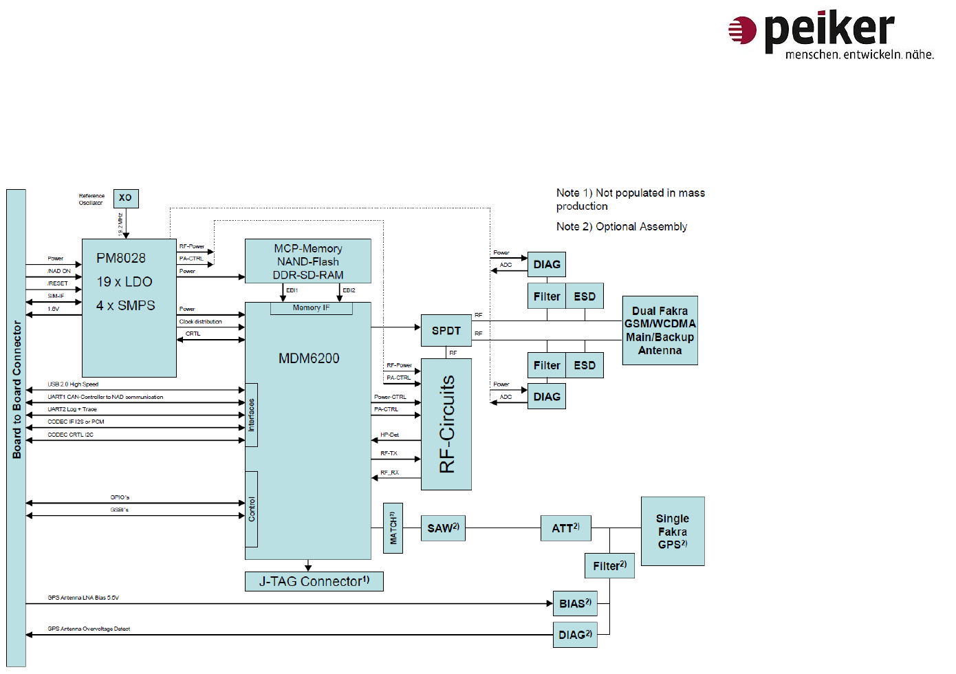
3. Overview HW – Part
3.1. Block – Diagram
Figure 1: Block diagram of NAD6200 module

________________________________________________________________________________________________________________________________________ Site 15
peiker acustic GmbH & Co. KG, Max-Planck-Straße 28-32, D-61381 Friedrichsdorf, Amtsgericht Bad Homburg HRA 1897
phG: peiker Verwaltungs GmbH, Vorsitzender der Geschäftsführung: Andreas Peiker, Geschäftsführer: Reinhard Kromer-von Baerle, Amtsgericht Bad Homburg HRB 1369
Vorsitzender des Aufsichtsrates: Dr. Helmut Rothenberger Ein Unternehmen der peiker Firmengruppe
3.2. Pin description of the board to board connector
The following table describes the pin out of the board to board connector of the NAD6200 Module. For
detailed information about the electrical characteristics of every Pin see chapter 3.3.2 Detailed Pin
description.
Table 4: Pin description of the board to board connector
PIN
Signal
Direction
related to
NAD6200
Comment
1
VPH_PWR
Input Power
Main Power
2
GND
Input Power
Power GND
3
VPH_PWR
Input Power
Main Power
4
GND
Input Power
Power GND
5
VPH_PWR
Input Power
Main Power
6
GND
Input Power
Power GND
7
KPD_POWER
IN / active low
NAD6200 switch on input
8
VREG_MSME
Output Power
Output power
9
USIM_RST
Output
SIM – Card reset
10
USIM_CLK
Output
SIM – Card clock
11
VREG_USIM
Output Power
Output power to SIM – Card
12
USIM_DATA
IN/OUT
SIM – Card data
13
GPIO_73
I/O
GPIO
14
GPIO_69
I/O
GPIO
15
GPIO_32_GSBI_1_0
Output
4 - Pin – UART – Ready for receive 1
16
RES_IN
IN
Force a reset, shut down the PMIC
17
GPIO_35_GSBI_1_3
Output
4 - Pin - UART - TX 1
18
GPIO_33_GSBI_1_1
Input
4 - Pin - UART - clear to send 1
19
GPIO_30_GSBI_0_2
Input
2 - Pin - UART - RX 2
20
GPIO_34_GSBI_1_2
Input
4 - Pin - UART - RX 1
21
GPIO_47_GSBI_4_3
Output
I²S - Master Clock
22
GPIO_31_GSBI_0_3
Output
2 - Pin - UART - TX 2
23
USB_DP
IN/OUT
High – Speed USB Device for
communication
24
USB_VBUS
Input Power
High – Speed USB Device for
communication
25
USB_DM
IN/OUT
High – Speed USB Device for
communication
26
GND_USB
Power
High – Speed USB Device for
communication
27
GPIO_38_GSBI_2_2
Output
I²S - Master Clock
28
GPIO_37_GSBI_2_1
Output
I²S - word select
29
GPIO_36_GSBI_2_0
Output
I²S - clock
30
GPIO_39_GSBI_2_3
Input
I²S - data input
31
GPIO_42_GSBI_3_2
Input
2 – Pin – UART – RX 3
32
GPIO_43_GSBI_3_3
Output
2 – Pin – UART – TX 3
33
GPIO_40_GSBI_3_0
Output
I²C – seriel clock
34
GPIO_41_GSBI_3_1
IN/OUT
I²C – serial data
________________________________________________________________________________________________________________________________________ Site 16
peiker acustic GmbH & Co. KG, Max-Planck-Straße 28-32, D-61381 Friedrichsdorf, Amtsgericht Bad Homburg HRA 1897
phG: peiker Verwaltungs GmbH, Vorsitzender der Geschäftsführung: Andreas Peiker, Geschäftsführer: Reinhard Kromer-von Baerle, Amtsgericht Bad Homburg HRB 1369
Vorsitzender des Aufsichtsrates: Dr. Helmut Rothenberger Ein Unternehmen der peiker Firmengruppe
35
GPIO_17
Output
NAD-WAKEUP
36
GPIO_14
Output
Codec Reset
37
GPIO_46_GSBI_4_2
Output
I²S – data output
38
GPIO_9
Input
NAD-UPDATE
39
GPS_ANT_OVERVOLT
OUT / active
low
Detection of GPS – Antenna short
against + 12 V
40
EXT_5V5
Input Power
Power for inside GPS – Antenna LNA
Information about the pin connector and mating connector:
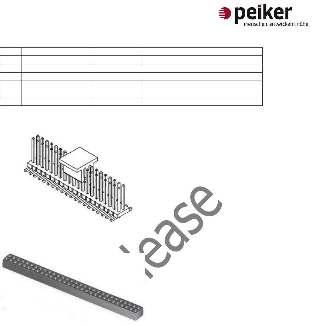
Figure 2: board to board pin connector
Figure 3: Mating connector
For detailed information about board to board pin connector see reference 1 and for mating connector
see reference 2. Both are in the Table 1: References.
________________________________________________________________________________________________________________________________________ Site 17
peiker acustic GmbH & Co. KG, Max-Planck-Straße 28-32, D-61381 Friedrichsdorf, Amtsgericht Bad Homburg HRA 1897
phG: peiker Verwaltungs GmbH, Vorsitzender der Geschäftsführung: Andreas Peiker, Geschäftsführer: Reinhard Kromer-von Baerle, Amtsgericht Bad Homburg HRB 1369
Vorsitzender des Aufsichtsrates: Dr. Helmut Rothenberger Ein Unternehmen der peiker Firmengruppe
3.3. HW – Features
3.3.1. W-WAN connectivity
3.3.1.1. GSM/EDGE
- EGSM850,900 Class 4 (2W)
- GSM1800, 1900 Class 1 (1W)
- EDGE850, EDGE900 Class E2 (0.5W)
- EDGE1800, EDGE1900 Class E2 (0.4W)
- GPRS/EDGE Multi slot class 12
- DTM Multi slot class 11
3.3.1.2. UMTS/WCDMA
UMTS / WCDMA are the 3rd generation of mobile telecommunication standard worldwide. HSPA are only
an extension of UMTS / WCDMA.
- WCDMA up to 384 kb/s at uplink/downlink
- UMTS to GSM handover for both voice and data
- HSPA:
HSDPA: Downlink with at least 14.4. Mbit/s
HSUPA: Uplink with at least 5.7 Mbit/s
Three different license configurations are realizable for Peiker NAD6200:
- UMTS Standard with Downlink Rate 384 kBit/s as license option (LDR)
- UMTS HSDPA with Downlink Rate 3.6 MBit/s as license option
- UMTS HSDPA+ with Downlink Rate 14.4 MBit/s as license option
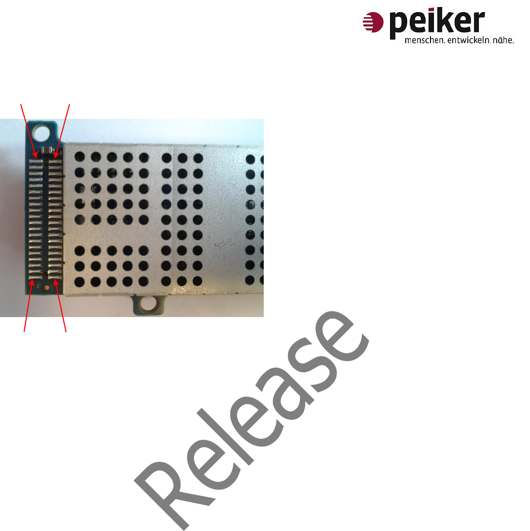
PIN 2
PIN 1
PIN 40
PIN 39
________________________________________________________________________________________________________________________________________ Site 18
peiker acustic GmbH & Co. KG, Max-Planck-Straße 28-32, D-61381 Friedrichsdorf, Amtsgericht Bad Homburg HRA 1897
phG: peiker Verwaltungs GmbH, Vorsitzender der Geschäftsführung: Andreas Peiker, Geschäftsführer: Reinhard Kromer-von Baerle, Amtsgericht Bad Homburg HRB 1369
Vorsitzender des Aufsichtsrates: Dr. Helmut Rothenberger Ein Unternehmen der peiker Firmengruppe
3.3.1.3. GNSS
GNSS is used for detection of the position and navigation. In the moment two systems are exist the
American version GPS and the Russian version GLONASS.
The NAD6200 support GPS and GLONASS.
The MDM GNSS RF receiver performance is adequate to ensure compliance to the applicable standards.
3.3.1.3.1. GPS
Table 5: Features of the GPS
Feature
Value
Comment
Acquisition sensitivity – MSA
Asynchronous A-GPS
-158 dBm
Cold – start sensitivity
-145 dBm
Tracking sensitivity
Standalone or MSB
-161 dBm
Accuracy in open sky
<2m CEP-50
Open sky, 1 Hz tracking
Standalone time to first fix
(super hot/warm/cold/weak signal)
1s / 29s / 32s / 50s
3.3.1.3.2. GLONASS
Table 6: Characteristics of GLONASS
Feature
Value
comment
Tracking sensitivity 98%
-155.3 dBm
-155.3 dBm
Probability of detection (Pdet) = 0.98
Probability of false alarm (Pfa) = 1e-3
Tracking sensitivity 98 %
normalized to 2.5 dB NF
-158.2 dBm
-158.8 dBm
Predicted Mission mode
tracking sensitivity normalized
to 2.5 dB NF, Pdet = 50%
-160.3 dBm
-160.9 dBm
3.3.2. Detailed Pin description
3.3.2.1. Power Supply
The NAD6200 Module has 3 Pins (PIN 1, PIN 3 and PIN 5) for the Main Power Supply Voltage
(VPH_PWR) and 3 Pins (PIN 2, PIN 4, PIN 6) for the Power Ground (GND).
3.3.2.1.1. Absolute maximum values
Voltage supply 3.4….4.2 V
Current supply 2.5 A @ peak
Temperature range -40°C…+85°C
________________________________________________________________________________________________________________________________________ Site 19
peiker acustic GmbH & Co. KG, Max-Planck-Straße 28-32, D-61381 Friedrichsdorf, Amtsgericht Bad Homburg HRA 1897
phG: peiker Verwaltungs GmbH, Vorsitzender der Geschäftsführung: Andreas Peiker, Geschäftsführer: Reinhard Kromer-von Baerle, Amtsgericht Bad Homburg HRB 1369
Vorsitzender des Aufsichtsrates: Dr. Helmut Rothenberger Ein Unternehmen der peiker Firmengruppe
3.3.2.1.2. Nominal values
Table 7: nominal values of the NAD6200 - module
Parameter
Min
Typ
Max
Unit
Voltage supply
3.7
3.8
3.9
V
Current supply
2.5
A
Voltage drop @ GSM
power burst (33 dBm)
for an external voltage
regulator
100
mV
3.3.2.2. KPD_Power
3.3.2.2.1. Description
This signal is used to switch on the NAD6200 module.
After the main power VPH_Power (3.8V) is applied to the NAD6200 module, the module will not start
automatically. To start the power regulators of the module KPD_Power must be pulled against ground
for at least 60 ms.
KPD_POWER input has an internal weak pull up against VPH_Power. Due to this fact it is recommended
to pull the input against GND using an open drain or open collector circuit.
Because of EMC constraints it might be necessary to add an additional stronger pull up against the
VPH_Power.
It is also possible to connect the KPD_Power input directly to Ground. In this case the module will start
up immediately after VPH_Power turned on.
3.3.2.2.2. Electrical characteristics
Table 8: Electrical characteristics of KPD_Power
PIN
Parameter
Comment
7
KPD_POWER
Pull down with
open Collector
3.3.2.3. RES_IN
3.3.2.3.1. Description
The reset input can be used either to switch off the module or to reset the module. In case that the
module is already powered on and the KPD_Power is in pull up state this signal must be driven against
ground for 250 ms to switch off the module. The module will remain switched off until the reset signal is
released to pull up state and until there is no new KPD_Power on sequence.
In case of that the KPD_Power pin is connected directly to ground the internal regulators of the module
will also switch off, but only for a few ms and then a new power on sequence starts automatically.
RES_IN input has an internal weak pull up against VREG_MSME (1.8V). Due to this fact it is
recommended to pull the input against GND using an open drain or open collector circuit.
Because of EMC constraints it might be necessary to add an additional stronger pull up against the
VREG_MSME (1.8V).
________________________________________________________________________________________________________________________________________ Site 20
peiker acustic GmbH & Co. KG, Max-Planck-Straße 28-32, D-61381 Friedrichsdorf, Amtsgericht Bad Homburg HRA 1897
phG: peiker Verwaltungs GmbH, Vorsitzender der Geschäftsführung: Andreas Peiker, Geschäftsführer: Reinhard Kromer-von Baerle, Amtsgericht Bad Homburg HRB 1369
Vorsitzender des Aufsichtsrates: Dr. Helmut Rothenberger Ein Unternehmen der peiker Firmengruppe
3.3.2.3.2. Electrical characteristics
Table 9: Electrical characteristics of RES_IN
PIN
Parameter
Comment
16
RES_IN
Pull down with
open Collector
3.3.2.4. VREG_MSME
3.3.2.4.1. Description
VREG_MSME is provided by an internal regulator of the NAD6200 module. VREG_MSME can be used to
source interface circuits like level shifters which are connected to the interfaces or GPIOs of the
NAD6200 module.
The current drawn on VREG_MSME shall not exceed 30 mA. When using VREG_MSME it is
recommended to decouple the signal with a combination of 1 µF and 22 pF directly at the board to
board connector.
3.3.2.4.2. Electrical characteristics
Table 10: Electrical characteristics of VREG_MSME
PIN
Parameter
Min
Max
Unit
Comment
8
VREG_MSME
1.8
V
30
mA
3.3.2.5. SIM Card
3.3.2.5.1. Description
The SIM interface of the NAD6200 module is compatible to 1.8 V and 3 V SIM Cards. Necessary voltage
and level shifting is handled by NAD6200 module automatically. The SIM interface consists of the
following signals:
- VREG_USIM: SIM Supply Voltage
- USIM_CLK: SIM clock signal
- USIM_DATA: SIM data signal
- USIM_RESET: SIM reset signal
- GPIO69: SIM Present Signal9
The data speed on the SIM interface is up to 4 Mbit. Hardware designer should take care of the length
and routing of the SIM interface to prevent potential problems.
9 : Software doesn´t support this feature at the moment.

________________________________________________________________________________________________________________________________________ Site 21
peiker acustic GmbH & Co. KG, Max-Planck-Straße 28-32, D-61381 Friedrichsdorf, Amtsgericht Bad Homburg HRA 1897
phG: peiker Verwaltungs GmbH, Vorsitzender der Geschäftsführung: Andreas Peiker, Geschäftsführer: Reinhard Kromer-von Baerle, Amtsgericht Bad Homburg HRB 1369
Vorsitzender des Aufsichtsrates: Dr. Helmut Rothenberger Ein Unternehmen der peiker Firmengruppe
3.3.2.5.2. Electrical characteristics
Table 11: Electrical characteristics of SIM Interface
PIN
Parameter
Min
Max
Unit
Comments
11
VREG_USIM
2.85 /
1.8
V
150
mA
10
USIM_CLK
2.85
/1.8
V
12
USIM_DATA
2.85
/1.8
V
Pull up 22 kΩ
against VREG_USIM
is required
9
USIM_RESET
2.85
/1.8
V
14
SIM Present Signal
– GPIO69
1.8
V
Is not supported yet
3.3.2.6. USB
3.3.2.6.1. Description
The NAD6200 module has one USB 2.0 high speed compliant interface with built-in PHY.
The USB Interface consists of 4 signals:
- USB_DP: USB Data Plus signal
- USB_DM: USB Data Minus signal
- USB_VBUS: USB Voltage Supply
- USB_GND: USB Ground
The NAD6200 module is configured as USB – Device on the NAD6200 PCB.
This Interface supports the following data rates:
- At low – speed: 1.5 Mbit/s
- At full – speed: 12 Mbit/s
- At high – speed: 480 Mbit/s
3.3.2.6.2. Electrical characteristics
Table 12: Electrical characteristics of USB Interface
PIN
Parameter
Min
Max
Unit
Comment
23
USB_DP
3.3
V
25
USB_DM
3.3
V
24
USB_VBUS
2
5.25
V
It is impossible to supply the module
with USB_VBUS only.
5
mA
26
USB_GND
If there is a requirement that the system must power the USB_VBUS while the module is not switched
on, it is strictly recommended to limit the USB_VBUS current to the module by a serial resistor of 22 KΩ.

________________________________________________________________________________________________________________________________________ Site 22
peiker acustic GmbH & Co. KG, Max-Planck-Straße 28-32, D-61381 Friedrichsdorf, Amtsgericht Bad Homburg HRA 1897
phG: peiker Verwaltungs GmbH, Vorsitzender der Geschäftsführung: Andreas Peiker, Geschäftsführer: Reinhard Kromer-von Baerle, Amtsgericht Bad Homburg HRB 1369
Vorsitzender des Aufsichtsrates: Dr. Helmut Rothenberger Ein Unternehmen der peiker Firmengruppe
The Pin USB_VBUS must be supply a Minimum voltage about 2 V with the serial resistor.
3.3.2.7. GPIOs
3.3.2.7.1. Description
There are 21 GPIOs on the board to board connector of the NAD6200 module. Most of them are part of
5 GSBIs and are used for different interfaces (see Table 4 and the following chapters).
For dissenting configurations of the GPIOs/GSBIs please contact Peiker acustics GmbH & Co.KG
GPIOs and GSBIs share the same output pins and may not available when used as GSBI configuration.
The following GPIOs are not belonging to a GSBI bundle:
GPIO 9, 14, 69, 17, 73
The following GPIOs are belonging to a GSBI bundle:
GPIO 30, 31, 32, 33, 34, 35, 36, 37, 38, 39, 40, 41, 42, 43, 46, 47
Available signals on GSBI bundles at the board to board connector:
- GSBI0: GSBI0_2, GSBI0_3 (GPIO_30, 31)
- GSBI1: GSBI1_0, GSBI1_1, GSBI1_2, GSBI1_3 (GPIO_32, 33, 34, 35)
- GSBI2: GSBI2_0, GSBI2_1, GSBI2_2, GSBI2_3 (GPIO_36, 37, 38, 39)
- GSBI3: GSBI3_0, GSBI3_1, GSBI3_2, GSBI3_3 (GPIO_40, 41, 42, 43)
- GSBI4: GSBI4_2, GSBI4_3 (GPIO_46, 47)
________________________________________________________________________________________________________________________________________ Site 23
peiker acustic GmbH & Co. KG, Max-Planck-Straße 28-32, D-61381 Friedrichsdorf, Amtsgericht Bad Homburg HRA 1897
phG: peiker Verwaltungs GmbH, Vorsitzender der Geschäftsführung: Andreas Peiker, Geschäftsführer: Reinhard Kromer-von Baerle, Amtsgericht Bad Homburg HRB 1369
Vorsitzender des Aufsichtsrates: Dr. Helmut Rothenberger Ein Unternehmen der peiker Firmengruppe
For the standard configuration of the GSBIs see the following Figure 4.
Figure 4: Pin description of GSBIs
For other configuration of the GSBIs please contact Peiker acustics GmbH & Co.KG.
3.3.2.7.2. Electrical characteristics
Table 13: Electrical characteristics of GPIOs
PIN
Parameter
Min
Max
Unit
Comment
13
GPIO_73
1.8
V
14
GPIO_69 -
SIM Present Signal
1.8
V
Not implemented yet.
Pull down 1 kΩ against
Ground
35
GPIO_17 –
NAD-WAKEUP
1.8
V
36
GPIO_14 –
Codec reset
1.8
V
________________________________________________________________________________________________________________________________________ Site 24
peiker acustic GmbH & Co. KG, Max-Planck-Straße 28-32, D-61381 Friedrichsdorf, Amtsgericht Bad Homburg HRA 1897
phG: peiker Verwaltungs GmbH, Vorsitzender der Geschäftsführung: Andreas Peiker, Geschäftsführer: Reinhard Kromer-von Baerle, Amtsgericht Bad Homburg HRB 1369
Vorsitzender des Aufsichtsrates: Dr. Helmut Rothenberger Ein Unternehmen der peiker Firmengruppe
38
GPIO_9 –
NAD-UPDATE
1.8
V
Pull up 10 kΩ against
1.8 V
The following table is valid for all GPIOs and digital inputs and outputs.
Table 14: Definition of High - and Low - Level for digital inputs and outputs
Parameter
Min
Typ
Max
Unit
VIH
High-level input
voltage
0.65*1.8
1.8+0.3
V
VIL
Low-level input
voltage
-0.3
0.35*1.8
V
VSHYS
Hysteresis voltage
100
mV
VOH
High-level output
voltage
1.8-0.45
1.8
V
VOL
Low-level output
voltage
0
0.45
V
3.3.2.8. UART
3.3.2.8.1. Description
The GPIOs 30, 31 and 42, 43 are configured as a 2 – Pin - UART and the GSBI1 are configured as a 4 –
Pin - UART. It is used for the following applications:
- The UART 1 is used for the communication between the NAD6200 module and a CAN Controller
- The UART 2 is used for log and trace
- The UART 3 is used for test and debug of the NAD6200 module
3.3.2.8.2. Electrical characteristics
Table 15: Electrical characteristics of UART Interfaces
PIN
Parameter
Min
Max
Unit
19
UART – RX2
1.8
V
22
UART – TX2
1.8
V
31
UART – RX3
1.8
V
32
UART – TX3
1.8
V
15
UART – RFR1
1.8
V
17
UART – TX1
1.8
V
18
UART – CTS1
1.8
V
20
UART – RX1
1.8
V
3.3.2.9. I²C
3.3.2.9.1. Description
The I²C – Interface is used for the communication between the CODEC and NAD6200 Module.

________________________________________________________________________________________________________________________________________ Site 25
peiker acustic GmbH & Co. KG, Max-Planck-Straße 28-32, D-61381 Friedrichsdorf, Amtsgericht Bad Homburg HRA 1897
phG: peiker Verwaltungs GmbH, Vorsitzender der Geschäftsführung: Andreas Peiker, Geschäftsführer: Reinhard Kromer-von Baerle, Amtsgericht Bad Homburg HRB 1369
Vorsitzender des Aufsichtsrates: Dr. Helmut Rothenberger Ein Unternehmen der peiker Firmengruppe
3.3.2.9.2. Electrical characteristics
Table 16: Electrical characteristics of I²C
PIN
Parameter
Min
Max
Unit
33
Seriel clock
1.8
V
34
Seriel data
1.8
V
3.3.2.10. I²S
3.3.2.10.1. Description
The I²S interface is used to transfer serial digital audio to/from an external stereo DAC/ADC. This
interface is a 3 – wire interface:
- Serial clock
- Word select
- Serial data
I²S supports all the Tx/Rx slave/master modes:
- Transmitter – master
- Transmitter – slave
- Receiver – master
- Receiver – slave
Master or slave is determined by the device driving the serial clock and word select. The transmitter
sends data to the receiver.
Bidirectional I²S support is supported by configuring two of the five GSBI ports as I²S; one GSBI as
transmitter and the second GSBI as receiver. Two options are possible:
- Option 1: MDM as master (transmitter or receiver) and slave (transmitter or receiver); external
device as slave. The MDM transmitter and receiver cannot both be the master at the same time as
there will be data contention.
- Option 2: Both MDM transmitter and receiver are slave; external device as master.
At the standard configuration the NAD6200 module is master and the Codec slave. For other
configuration please contact Peiker acustics GmbH & Co.KG.
3.3.2.10.2. Electrical characteristics
Table 17: Electrical characteristics of I²S
PIN
Parameter
Min
Max
Unit
27 /
21
Master Clock
1.8
V
28
Word Select
1.8
V
29
Clock
1.8
V
30
Data input
1.8
V
37
Data output
1.8
V
36
GPIO_14 – codec
reset
1.8
V
________________________________________________________________________________________________________________________________________ Site 26
peiker acustic GmbH & Co. KG, Max-Planck-Straße 28-32, D-61381 Friedrichsdorf, Amtsgericht Bad Homburg HRA 1897
phG: peiker Verwaltungs GmbH, Vorsitzender der Geschäftsführung: Andreas Peiker, Geschäftsführer: Reinhard Kromer-von Baerle, Amtsgericht Bad Homburg HRB 1369
Vorsitzender des Aufsichtsrates: Dr. Helmut Rothenberger Ein Unternehmen der peiker Firmengruppe
3.3.2.11. GPS Pins
3.3.2.11.1. Description
The PIN GPS_ANT_OVERVOLT and EXT_5V5 are reserved for use of the internal GPS of the NAD6200
module.
The PINs should be grounded when not used in the design.
3.3.2.11.2. Electrical characteristics
Table 18: Electrical characteristics of GPS Pins
PIN
Parameter
Min
Max
Unit
Comment
39
GPS_ANT_OVERVOLT
-
-
-
Open Collector, Pull up 47 kΩ
against 3.3 V
40
EXT_5V5
5.5
V
100
mA
3.3.3. Antenna
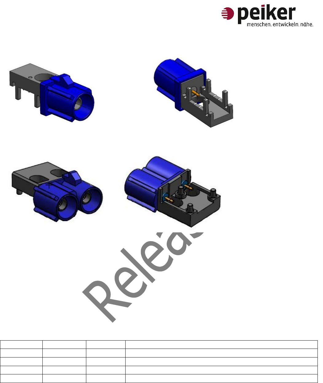
3.3.3.1. Antenna connector
The NAD6200 - module can be equipped with three antenna connectors. One connector is for the main
antenna, second connector is for the backup antenna and third connector is for the GNSS antenna. See
the following Figure 5: Antenna connectors.
SPDT
Figure 5: Antenna connectors
Main antenna
connector
Backup antenna
connector
Prepared GNSS
antenna connector
optional
________________________________________________________________________________________________________________________________________ Site 27
peiker acustic GmbH & Co. KG, Max-Planck-Straße 28-32, D-61381 Friedrichsdorf, Amtsgericht Bad Homburg HRA 1897
phG: peiker Verwaltungs GmbH, Vorsitzender der Geschäftsführung: Andreas Peiker, Geschäftsführer: Reinhard Kromer-von Baerle, Amtsgericht Bad Homburg HRB 1369
Vorsitzender des Aufsichtsrates: Dr. Helmut Rothenberger Ein Unternehmen der peiker Firmengruppe
Figure 6: FAKRA HF Single connector
Figure 7: FAKRA HF Dual connector
For detailed information see the datasheet of those connectors. The device numbers of connectors see
the reference 3 and 4 at the Table 1: References.
3.3.3.2. Antenna Switching
For switching between main and backup antenna a RF – switch SPDT is soldered on the PCB of the
NAD6200 – module. The switch is controlled by two GPIO´s. The following Table 19 shows 4 switch
combinations.
Table 19: switch combinations
GPIO_55
GPIO_56
Antenna
Comment
Low
Low
None
Whole transmission power would be reflected
Low
Hi
Main
Outside antenna connector
Hi
Low
Backup
Inside antenna connector
Hi
Hi
Both
Mismatching
The switching between different states must be synchronized with QCT software, because it is not
allowed to switch between main and backup antenna during the GSM transmission pulse.
The state GPIO_55 = Hi and GPIO_56 = Hi is not allowed and have to avoid via software.
At the moment the main antenna is switched on by default. The main antenna is mapped to SMB
connector close to outer dimension of the NAD6200 – module.

________________________________________________________________________________________________________________________________________ Site 28
peiker acustic GmbH & Co. KG, Max-Planck-Straße 28-32, D-61381 Friedrichsdorf, Amtsgericht Bad Homburg HRA 1897
phG: peiker Verwaltungs GmbH, Vorsitzender der Geschäftsführung: Andreas Peiker, Geschäftsführer: Reinhard Kromer-von Baerle, Amtsgericht Bad Homburg HRB 1369
Vorsitzender des Aufsichtsrates: Dr. Helmut Rothenberger Ein Unternehmen der peiker Firmengruppe
3.3.3.3. Antenna diagnostics
The diagnostic is supported for the main and backup antenna. The following states have to diagnose:
a) Antenna connected
b) No antenna connected
c) Antenna has a short-circuit against ground
d) Antenna has a short-cicuit against +Ubatt
The hardware is implemented for the diagnostic for both antenna on the PCB of the NAD6200 – module.
This hardware is connected to the PM8028. Main antenna is connected to MPP_08 and backup antenna
is connected to MPP_07.
The following expected voltage level is see at the ADC input with an external resistor R = 10 kOhm:
(ADCref = 2.2 V)
For a) about 850 mV
For b) about 1150 mV
For c) about 390 mV
For d) about 1900 mV
3.3.4. Chipset MDM6200 + PM8028
The NAD Module included a Chipset from Qualcomm. This Chipset consist of the power manager
PM8028 and mobile data modem MDM6200.
3.3.4.1. PM8028
The PMIC monitors and controls the power sources, detecting which sources are applied and verifying
that they are within acceptable operational limits. Thermal conditions of the integrated pass transistor
and its total current are monitored and reported to a state machine that coordinates PM operations.
Other input power management circuits provide VDD or VBAT voltage regulation, current monitoring and
over – current protection, VDD collapse protection, under – voltage lockout protection, and automated
recovery from sudden momentary power loss (SMPL).
On – chip voltage regulators generate 24 programmable output voltages using a combination of four
switched – mode power supplies, 19 low – dropout linear regulators.
3.3.4.2. MDM6200
The MDM6200 is a mobile data modem IC. They have the following functions:
-
Baseband functions:
Processors
Memory support
Connectivity
Air interfaces
Internal BB functions
Interfaces with other functions

________________________________________________________________________________________________________________________________________ Site 29
peiker acustic GmbH & Co. KG, Max-Planck-Straße 28-32, D-61381 Friedrichsdorf, Amtsgericht Bad Homburg HRA 1897
phG: peiker Verwaltungs GmbH, Vorsitzender der Geschäftsführung: Andreas Peiker, Geschäftsführer: Reinhard Kromer-von Baerle, Amtsgericht Bad Homburg HRB 1369
Vorsitzender des Aufsichtsrates: Dr. Helmut Rothenberger Ein Unternehmen der peiker Firmengruppe
General – purpose I/Os
-
RF functions:
RF transmitter (including supporting analog and LO circuits)
RF receiver (including supporting analog and LO circuits)
3.3.5. Memory
The NAD6200 – module has one 1 Gb NAND Flash + 512 Mb Mobile DDR SDRAM memory.
For more detailed information about the memory device see the datasheet of K521H12ACI-B050.

________________________________________________________________________________________________________________________________________ Site 30
peiker acustic GmbH & Co. KG, Max-Planck-Straße 28-32, D-61381 Friedrichsdorf, Amtsgericht Bad Homburg HRA 1897
phG: peiker Verwaltungs GmbH, Vorsitzender der Geschäftsführung: Andreas Peiker, Geschäftsführer: Reinhard Kromer-von Baerle, Amtsgericht Bad Homburg HRB 1369
Vorsitzender des Aufsichtsrates: Dr. Helmut Rothenberger Ein Unternehmen der peiker Firmengruppe
4. Application software
Tbd

________________________________________________________________________________________________________________________________________ Site 31
peiker acustic GmbH & Co. KG, Max-Planck-Straße 28-32, D-61381 Friedrichsdorf, Amtsgericht Bad Homburg HRA 1897
phG: peiker Verwaltungs GmbH, Vorsitzender der Geschäftsführung: Andreas Peiker, Geschäftsführer: Reinhard Kromer-von Baerle, Amtsgericht Bad Homburg HRB 1369
Vorsitzender des Aufsichtsrates: Dr. Helmut Rothenberger Ein Unternehmen der peiker Firmengruppe
5. Antenna characteristics
5.1. Electrical characteristics for the Antenna
The end user is responsible to take care of the fulfillment of the “over the air performance” (OTA) of his
end product.
OTA performance will be influenced mainly by the RF routing from the module to the antenna and
antenna choice. If external switches or splitters are necessary signal attenuation and degradation has to
be considered.
Regulatory requirements will give details on measurements and the corresponding limits.
As an example 3GPP requirements are found in TS34.114 (user equipment/mobile station Over The Air
antenna performance; Conformance testing).
5.2. Electrical characteristics for the Bands
5.2.1. Frequencies
Table 20: Frequencies of supported WCDMA Bands for uplink
Band
Min
Typ
Max
Unit
WCDMA BC1
1920
-
1980
MHz
WCDMA BC2
1850
-
1910
MHz
WCDMA BC5
824
-
849
MHz
WCDMA BC8
880
-
915
MHz
Table 21: Frequencies of supported WCDMA Bands for downlink
Band
Min
Typ
Max
Unit
WCDMA BC1
2110
-
2170
MHz
WCDMA BC2
1930
-
1990
MHz
WCDMA BC5
869
-
894
MHz
WCDMA BC8
925
-
960
MHz
Table 22: Frequencies of supported GSM Bands (Uplink)
Band
Min
Typ
Max
Unit
GSM 850
824
-
849
MHz
GSM 900
876
-
915
MHz
GSM 1800
1710
-
1785
MHz
GSM 1900
1850
-
1910
MHz
Table 23: Frequencies of supported GSM Bands (Downlink)
Band
Min
Typ
Max
Unit
GSM 850
869
-
894
MHz
GSM 900
921
-
960
MHz
GSM 1800
1805
-
1880
MHz
GSM 1900
1930
-
1990
MHz

________________________________________________________________________________________________________________________________________ Site 32
peiker acustic GmbH & Co. KG, Max-Planck-Straße 28-32, D-61381 Friedrichsdorf, Amtsgericht Bad Homburg HRA 1897
phG: peiker Verwaltungs GmbH, Vorsitzender der Geschäftsführung: Andreas Peiker, Geschäftsführer: Reinhard Kromer-von Baerle, Amtsgericht Bad Homburg HRB 1369
Vorsitzender des Aufsichtsrates: Dr. Helmut Rothenberger Ein Unternehmen der peiker Firmengruppe
5.2.2. Power Consumption, Call
Table 24: Power Consumption @ TA = +25°C, VPH_PWR = 3.8 V, P = 23 dBm
Band
Condition
Min
Typ
Max
Unit
WCDMA BC1
REL 99
-
584
-
mA
WCDMA BC2
-
607
-
mA
WCDMA BC5
-
620
-
mA
WCDMA BC8
-
607
-
mA
Table 25: Power Consumption @ TA = +25°C, VPH_PWR = 3.8 V, P = 10 dBm
Band
Condition
Min
Typ
Max
Unit
WCDMA BC1
REL 99
-
192
-
mA
WCDMA BC2
-
196
-
mA
WCDMA BC5
-
184
-
mA
WCDMA BC8
-
297
-
mA
Table 26: Power Consumption @ TA = +25°C, VPH_PWR = 3.8 V, P = 0 dBm
Band
Condition
Min
Typ
Max
Unit
WCDMA BC1
REL 99
-
145
-
mA
WCDMA BC2
-
147
-
mA
WCDMA BC5
-
139
-
mA
WCDMA BC8
-
143
-
mA
Table 27: Power Consumption @ TA = +25°C, VPH_PWR = 3.8 V, Single Slot
Band
Condition
Min
Typ
Max
Unit
GSM 850
PCL = 5,
P = 33 dBm
-
324
-
mA
PCL = 19,
P = 5 dBm
-
117
-
GSM 900
PCL = 5,
P = 33 dBm
-
332
-
mA
PCL = 19
P = 5 dBm
-
118
-
GSM 1800
PCL = 0
P = 30 dBm
-
223
-
mA
PCL = 15
P = 0 dBm
-
117
-
GSM 1900
PCL = 0
P = 30 dBm
-
223
-
mA
PCL = 15
P = 0 dBm
-
117
-
Table 28: Idle current for GSM and WCDMA
Parameter
Condition
Min
Typ
Max
Unit
Idle current
GSM 900,
DRX = 5,
Vdd = 3.8 V
2.7
mA

________________________________________________________________________________________________________________________________________ Site 33
peiker acustic GmbH & Co. KG, Max-Planck-Straße 28-32, D-61381 Friedrichsdorf, Amtsgericht Bad Homburg HRA 1897
phG: peiker Verwaltungs GmbH, Vorsitzender der Geschäftsführung: Andreas Peiker, Geschäftsführer: Reinhard Kromer-von Baerle, Amtsgericht Bad Homburg HRB 1369
Vorsitzender des Aufsichtsrates: Dr. Helmut Rothenberger Ein Unternehmen der peiker Firmengruppe
Idle current
WCDMA BC1,
DRX = 8,
Vdd = 3.8 V
2.2
mA

________________________________________________________________________________________________________________________________________ Site 34
peiker acustic GmbH & Co. KG, Max-Planck-Straße 28-32, D-61381 Friedrichsdorf, Amtsgericht Bad Homburg HRA 1897
phG: peiker Verwaltungs GmbH, Vorsitzender der Geschäftsführung: Andreas Peiker, Geschäftsführer: Reinhard Kromer-von Baerle, Amtsgericht Bad Homburg HRB 1369
Vorsitzender des Aufsichtsrates: Dr. Helmut Rothenberger Ein Unternehmen der peiker Firmengruppe
6. Environmental Specification
6.1. General information
- Storage Temperature -40°C - +85°C
- Handling ESD – human body rating specified with max. 2 KV
6.2. Temperature Range
Table 29: Operating temperature range
Range
Operating temp. range
-30°C … +70°C
3GPP spec. conform
Operating temp. range
-40°C … +85°C 10
Operational
Performance might slightly
deviate from 3GPP spec.
10: Due to temperature specification of the chipset, the temperature of the power manager and the temperature of the modem
chip shall not exceed +85°C.
________________________________________________________________________________________________________________________________________ Site 35
peiker acustic GmbH & Co. KG, Max-Planck-Straße 28-32, D-61381 Friedrichsdorf, Amtsgericht Bad Homburg HRA 1897
phG: peiker Verwaltungs GmbH, Vorsitzender der Geschäftsführung: Andreas Peiker, Geschäftsführer: Reinhard Kromer-von Baerle, Amtsgericht Bad Homburg HRB 1369
Vorsitzender des Aufsichtsrates: Dr. Helmut Rothenberger Ein Unternehmen der peiker Firmengruppe
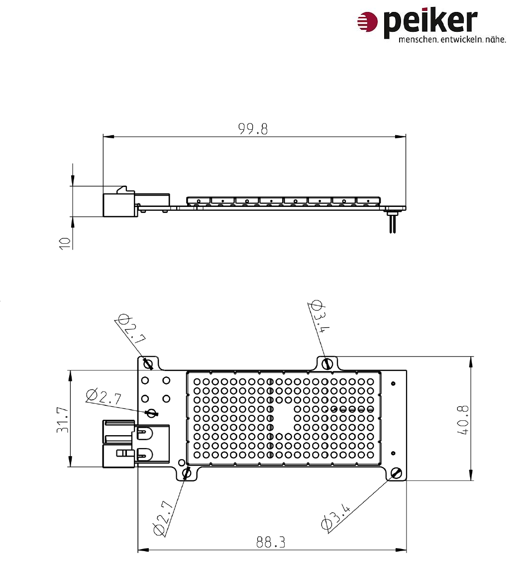
7. Mechanical Specification
Figure 8: Mechanical dimensions of the NAD6200 module
Figure 9: Mechanical dimensions of the NAD6200 module (top view)

________________________________________________________________________________________________________________________________________ Site 36
peiker acustic GmbH & Co. KG, Max-Planck-Straße 28-32, D-61381 Friedrichsdorf, Amtsgericht Bad Homburg HRA 1897
phG: peiker Verwaltungs GmbH, Vorsitzender der Geschäftsführung: Andreas Peiker, Geschäftsführer: Reinhard Kromer-von Baerle, Amtsgericht Bad Homburg HRB 1369
Vorsitzender des Aufsichtsrates: Dr. Helmut Rothenberger Ein Unternehmen der peiker Firmengruppe
8. Safety Recommendations according to EN60950-1
This device must be supplied by a limited power source according to EN 60950-1.
The clearance and creep age distances required by the end product must be withheld when the module
is installed.
The cooling of the end product shall not negatively be influenced by the installation of the module.
________________________________________________________________________________________________________________________________________ Site 37
peiker acustic GmbH & Co. KG, Max-Planck-Straße 28-32, D-61381 Friedrichsdorf, Amtsgericht Bad Homburg HRA 1897
phG: peiker Verwaltungs GmbH, Vorsitzender der Geschäftsführung: Andreas Peiker, Geschäftsführer: Reinhard Kromer-von Baerle, Amtsgericht Bad Homburg HRB 1369
Vorsitzender des Aufsichtsrates: Dr. Helmut Rothenberger Ein Unternehmen der peiker Firmengruppe
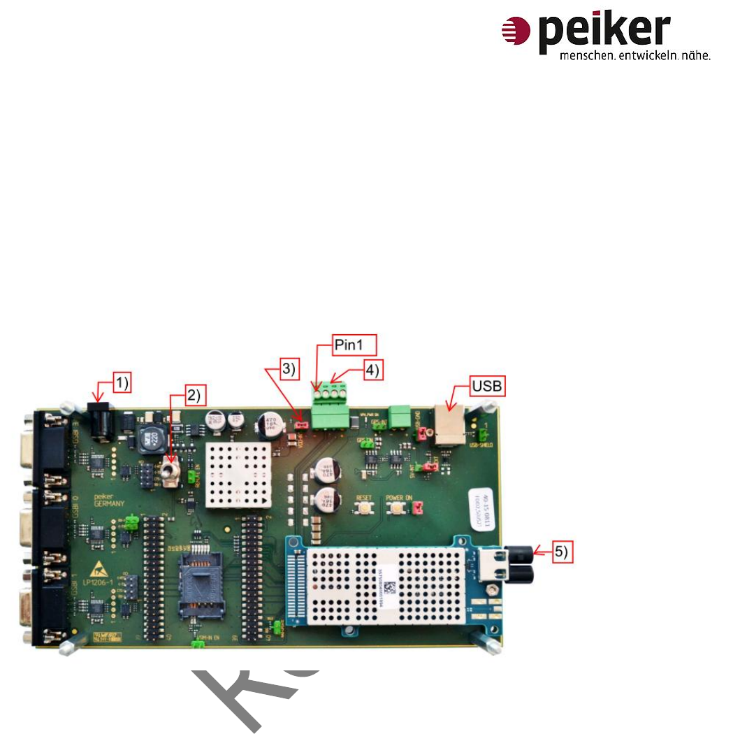
9. Evaluation Kit
For the NAD6200 – module there is an evaluation board available.
They have the following features:
- On beard 12 V DC power Supply or 3.8 V DC direct connected (unbuffered)
- USB 2.0 port type B
- SIM card tray
- 40 pin header connected to the board to board connector of the NAD6200 – module.
- 3 GSBI ports connected to DB9 or pin header.
Figure 10: Evaluation Kit for NAD6200 module
Using the evaluation board with on board 3.8 V regulator:
- Connect between 11 and 14 V DC to power connector 1) by using delivered cable
- Power up on the board with switch 2)
Using the evaluation board with an external power supply:
- Remove Jumper 3)
- Switch 2) to off condition
- Connect external supply between 3.6 and 4.0 V DC to connector 4)
- Connector 4) Pin out: Pin 1: GND
Pin 2: Sense GND
Pin 3: Sense V+
Pin 4: V+
Note: Make sure that the external power supply is not generating spikes or hazards higher
than 4.2 V. NAD6200 module gets damaged when spikes or hazards are above 4.2 V.
RF Connector:

________________________________________________________________________________________________________________________________________ Site 38
peiker acustic GmbH & Co. KG, Max-Planck-Straße 28-32, D-61381 Friedrichsdorf, Amtsgericht Bad Homburg HRA 1897
phG: peiker Verwaltungs GmbH, Vorsitzender der Geschäftsführung: Andreas Peiker, Geschäftsführer: Reinhard Kromer-von Baerle, Amtsgericht Bad Homburg HRB 1369
Vorsitzender des Aufsichtsrates: Dr. Helmut Rothenberger Ein Unternehmen der peiker Firmengruppe
For RF measurements use main antenna connector 5)
AT Command interface:
The module supports standard AT command as listed in the chapter 10.1 AT Command list.
Commands are compliant to: 3GPP TS 27.007
3GPP TS 27.005

________________________________________________________________________________________________________________________________________ Site 39
peiker acustic GmbH & Co. KG, Max-Planck-Straße 28-32, D-61381 Friedrichsdorf, Amtsgericht Bad Homburg HRA 1897
phG: peiker Verwaltungs GmbH, Vorsitzender der Geschäftsführung: Andreas Peiker, Geschäftsführer: Reinhard Kromer-von Baerle, Amtsgericht Bad Homburg HRB 1369
Vorsitzender des Aufsichtsrates: Dr. Helmut Rothenberger Ein Unternehmen der peiker Firmengruppe
10. Appendix
10.1. AT Command list
Table 30: AT Command list with description
Command
Description
Comment
AT+CMGF
Message Format
AT+CSCA
Service Centre Address
AT+CMGS
Send Message
AT+CGMI
Manufacturer Identification
AT+CGMM
Request model identification
AT+CGMR
Request revision identification
AT+CGSN
Request product serial number
AT+CIMI
Request international mobile subscriber
identification
AT+CMOD
Call mode
Only one Parameter is supported by the
device.
AT+CHUP
Hang up call
ATD
Initiate a CS or PS call or supplementary
service
ATA
Answer incoming CS call command
ATH
Hang-up CS call command
AT+CBST
Select bearer service type
AT+CEER
Extended error report
AT+CVHU
Voice hang-up control
AT+CREG
Network registration
AT+COPS
PLMN selection
AT+CLCK
Facility lock
AT+CPWD
Change password
AT+CLIP
Calling line identification presentation
AT+CLIR
Calling line identification restriction
AT+CCWA
Call waiting
AT+CHLD
Call related supplementary services
AT+CUSD
Unstructured supplementary service data
AT+CLCC
List current calls
AT+CPOL
Preferred PLMN list
AT+CPAS
Phone active status
AT+CFUN
Set phone functionality
AT+CPIN
Enter PIN
AT+CSQ
Signal quality
AT+CMER
Mobile termination event reporting
AT+CSIM
Generic SIM access
AT+CRSM
Restricted SIM access
AT+CMEE
Report mobile termination error
AT+CGDCONT
Define PDP context
AT+CGEQREQ
Request 3G quality of service profile
AT-CGATT
PS attach or detach

________________________________________________________________________________________________________________________________________ Site 40
peiker acustic GmbH & Co. KG, Max-Planck-Straße 28-32, D-61381 Friedrichsdorf, Amtsgericht Bad Homburg HRA 1897
phG: peiker Verwaltungs GmbH, Vorsitzender der Geschäftsführung: Andreas Peiker, Geschäftsführer: Reinhard Kromer-von Baerle, Amtsgericht Bad Homburg HRB 1369
Vorsitzender des Aufsichtsrates: Dr. Helmut Rothenberger Ein Unternehmen der peiker Firmengruppe
Command
Description
Comment
AT+CGACT
PDP context activate or deactivate
AT+CGPADDR
Show PDP address
AT+CGSMS
Select service for MO SMS messages
ATE
Character Echo ON/OFF
AT+CSMS
Check Message Service support
AT+CSMP
Set Text Mode Parameters
AT+CSDH
Show Text Mode Parameters
AT+CSCB
Select Cell Broadcast Message Types
AT+CSAS
Save Settings
Only one Parameter is supported by the
device.
AT+CRES
Restore Settings
Only one Parameter is supported by the
device.
AT+CMGL
List messages
AT+CNMA
New message acknowledgement
AT+CMGC
Send Command
AT+CMMS
More Messages to Send
AT+ATV
DCE response format
AT+ATX
Result code selection and call progress
monitoring control
AT+CNMI
New Message Indications to TE
AT+CPMS
Preferred Message Storage
AT+CMGW
Write Message to Memory
AT+CMSS
Send Message from Storage
AT+CMGD
Delete Messages
AT+CNUM
Get MSISDN
AT+CPBS
Select phonebook memory storage
AT+CPBR
Read phonebook entries
AT+CPBW
Write phonebook entry
10.2. Warning Statements
FCC
NOTE: This equipment has been tested and found to comply with the limits for a Class B digital device,
pursuant to part 15 of the FCC Rules. These limits are designed to provide reasonable protection against
harmful interference in a residential installation. This equipment generates, uses, and can radiate radio
frequency energy and, if not installed and used in accordance with the instructions, may cause harmful
interference to radio communications. However, there is no guarantee that interference will not occur in
a particular installation. If this equipment does cause harmful interference to radio or television
reception, which can be determined by turning the equipment off and on, the user is encouraged to try
to correct the interference by one or more of the following measures:
- Reorient or relocate the receiving antenna.
- Increase the separation between the equipment and receiver.
- Connect the equipment into an outlet on a circuit different from that to which the receiver is
connected.
- Consult the dealer or an experienced radio/TV technician for help.

________________________________________________________________________________________________________________________________________ Site 41
peiker acustic GmbH & Co. KG, Max-Planck-Straße 28-32, D-61381 Friedrichsdorf, Amtsgericht Bad Homburg HRA 1897
phG: peiker Verwaltungs GmbH, Vorsitzender der Geschäftsführung: Andreas Peiker, Geschäftsführer: Reinhard Kromer-von Baerle, Amtsgericht Bad Homburg HRB 1369
Vorsitzender des Aufsichtsrates: Dr. Helmut Rothenberger Ein Unternehmen der peiker Firmengruppe
(c) The provisions of paragraphs (a) and (b) of this section do not apply to digital devices exempted
from the technical standards under the provisions of § 15.103.
(d) For systems incorporating several digital devices, the statement shown in paragraph (a) or (b) of this
section needs to be contained only in the instruction manual for the main control unit.
(e) In cases where the manual is provided only in a form other than paper, such as on a computer disk
or over the Internet, the information required by this section may be included in the manual in that
alternative form, provided the user can reasonably be expected to have the capability to access
information in that form.
This device complies with Part 15 of the FCC rules. Operation is subject to the following two conditions:
(1) this device may not cause harmful interference, and
(2) this device must accept any interference received, including interference that may cause undesired
operation.
OEM responsibility to the FCC rules and regulations
The US variant without GNSS of the NAD 6200 module is labeled with its own FCC ID Number and IC ID
Number. If the FCC ID is not visible when the NAD6200 module is installed inside another device, then
the host device must contain the FCC ID number with the statement such as the following: “Contains
Transmitter Module FCC ID: QWY-PNADA or Contains FCC ID: QWY-PNADA”.
The US variant with GNSS of the NAD 6200 module is labeled with its own FCC ID Number and IC ID
Number. If the FCC ID is not visible when the NAD6200 module is installed inside another device, then
the host device must contain the FCC ID number with the statement such as the following: “Contains
Transmitter Module FCC ID: QWY-PNADB or Contains FCC ID: QWY-PNADB”.
Modifications
The FCC requires the user to be notified that any changes or modifications made to this device that are
not expressly approved by peiker acustic GmbH & Co. KG could void the user's authority to operate the
equipment.
RF Exposure Warning:
This equipment complies with FCC radiation exposure limits set forth for an uncontrolled environment.
This equipment should be installed and operated with minium distance 20 cm between the radiator and
your body. This transmitter must not be co-located or Operating in conjunction with any other antenna
or transmitter.
Notice:
The preceding statement must be included as a Caution statement in OEM product manuals in order to
alert users of FCC RF Exposure compliance.

________________________________________________________________________________________________________________________________________ Site 42
peiker acustic GmbH & Co. KG, Max-Planck-Straße 28-32, D-61381 Friedrichsdorf, Amtsgericht Bad Homburg HRA 1897
phG: peiker Verwaltungs GmbH, Vorsitzender der Geschäftsführung: Andreas Peiker, Geschäftsführer: Reinhard Kromer-von Baerle, Amtsgericht Bad Homburg HRB 1369
Vorsitzender des Aufsichtsrates: Dr. Helmut Rothenberger Ein Unternehmen der peiker Firmengruppe
IC Canada
This Class b digital apparatus complies with Canadian ICES-003.
Cet appareil numérique de la classe b est conforme à la norme NMB-003 du Canada.
Le présent appareil est conforme aux CNR d'Industrie Canada applicables aux appareils radio exempts
de licence. L'exploitation est autorisée aux deux conditions suivantes : (1) l'appareil ne doit pas produire
de brouillage, et (2) l'utilisateur de l'appareil doit accepter tout brouillage radioélectrique subi, même si
le brouillage est susceptible d'en compromettre le fonctionnement.