VTech Telecommunications 80-4258-05 SPP-ID970 Cordless Telephone User Manual RF Module Theory of Operation

VTech Telecommunications Ltd SPP-ID970 Cordless Telephone RF Module Theory of Operation

Contents

RF Module Theory of Operation

VTECH ENGINEERING CANADA LIMITEDTITLE PDL MK3 with U2768 RF Theory Of OperationMODEL Sony 970Reference: Revision: 0 Page: 1 of 29This document is proprietary to VTECH ENGINEERING CANADA LTD. 107274Specifications are preliminary and are subject to change without notice.PDL MK3 with U2768RF ModuleTHEORY OF OPERATIONNote:  All rights reserved.  No part of this publication may be reproduced or transmitted in any form or byany means.  The only controlled copy of this document is kept in electronic form on the VTECH computernetwork.  All printed copies are uncontrolled documents and are not updated.  This Procedure is theproperty of VTECH Engineering Canada Ltd., and shall be returned upon requestPrepared By John WangTitle RF EngineerChecked By Sarkis TeghararianTitle RF Development Manager
VTECH ENGINEERING CANADA LIMITEDTITLE PDL MK3 with U2768 RF Theory Of OperationMODEL Sony 970Reference: Revision: 0 Page: 2 of 29This document is proprietary to VTECH ENGINEERING CANADA LTD. 107274Specifications are preliminary and are subject to change without notice.Revision HistoryRevision No Description Page Effective Date0 Initial Release All June 9, 2000
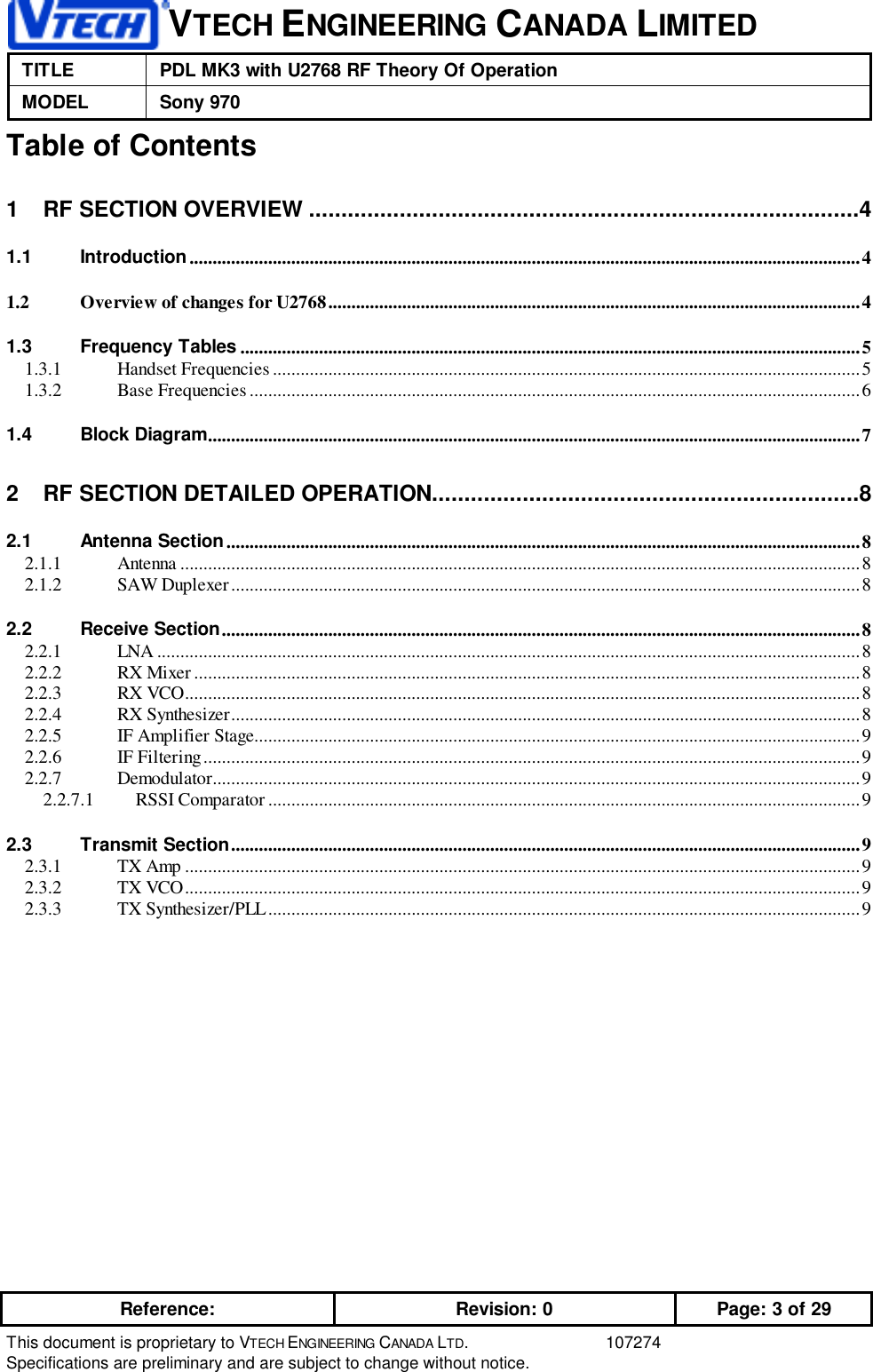
VTECH ENGINEERING CANADA LIMITEDTITLE PDL MK3 with U2768 RF Theory Of OperationMODEL Sony 970Reference: Revision: 0 Page: 3 of 29This document is proprietary to VTECH ENGINEERING CANADA LTD. 107274Specifications are preliminary and are subject to change without notice.Table of Contents1 RF SECTION OVERVIEW .....................................................................................41.1 Introduction.................................................................................................................................................41.2 Overview of changes for U2768...................................................................................................................41.3 Frequency Tables ......................................................................................................................................51.3.1 Handset Frequencies ...............................................................................................................................51.3.2 Base Frequencies ....................................................................................................................................61.4 Block Diagram.............................................................................................................................................72 RF SECTION DETAILED OPERATION..................................................................82.1 Antenna Section.........................................................................................................................................82.1.1 Antenna ...................................................................................................................................................82.1.2 SAW Duplexer........................................................................................................................................82.2 Receive Section..........................................................................................................................................82.2.1 LNA ........................................................................................................................................................82.2.2 RX Mixer ................................................................................................................................................82.2.3 RX VCO..................................................................................................................................................82.2.4 RX Synthesizer........................................................................................................................................82.2.5 IF Amplifier Stage...................................................................................................................................92.2.6 IF Filtering..............................................................................................................................................92.2.7 Demodulator............................................................................................................................................92.2.7.1 RSSI Comparator ................................................................................................................................92.3 Transmit Section........................................................................................................................................92.3.1 TX Amp ..................................................................................................................................................92.3.2 TX VCO..................................................................................................................................................92.3.3 TX Synthesizer/PLL................................................................................................................................9
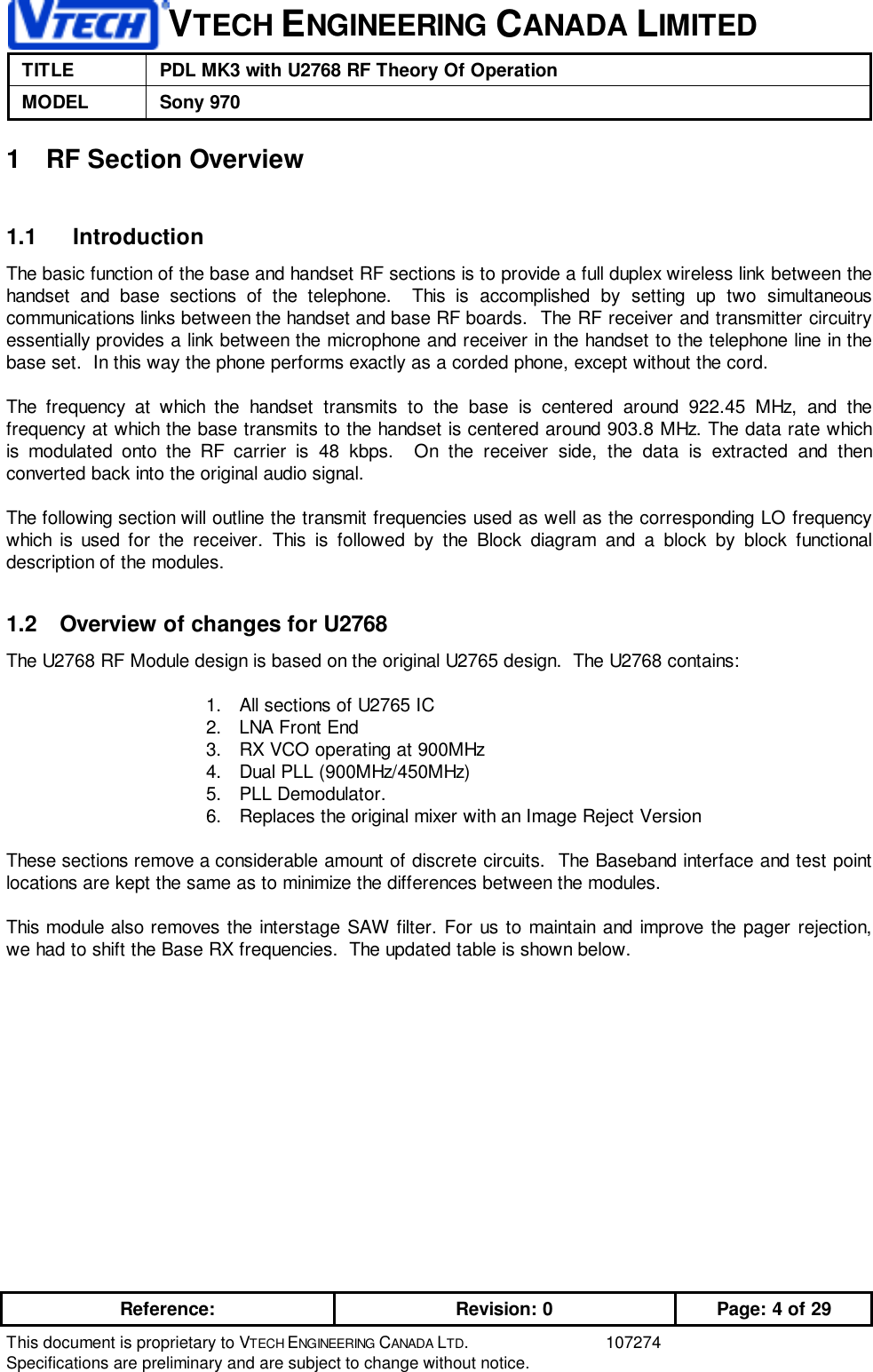
VTECH ENGINEERING CANADA LIMITEDTITLE PDL MK3 with U2768 RF Theory Of OperationMODEL Sony 970Reference: Revision: 0 Page: 4 of 29This document is proprietary to VTECH ENGINEERING CANADA LTD. 107274Specifications are preliminary and are subject to change without notice.1  RF Section Overview1.1 IntroductionThe basic function of the base and handset RF sections is to provide a full duplex wireless link between thehandset and base sections of the telephone.  This is accomplished by setting up two simultaneouscommunications links between the handset and base RF boards.  The RF receiver and transmitter circuitryessentially provides a link between the microphone and receiver in the handset to the telephone line in thebase set.  In this way the phone performs exactly as a corded phone, except without the cord.The frequency at which the handset transmits to the base is centered around 922.45 MHz, and thefrequency at which the base transmits to the handset is centered around 903.8 MHz. The data rate whichis modulated onto the RF carrier is 48 kbps.  On the receiver side, the data is extracted and thenconverted back into the original audio signal.The following section will outline the transmit frequencies used as well as the corresponding LO frequencywhich is used for the receiver. This is followed by the Block diagram and a block by block functionaldescription of the modules.1.2  Overview of changes for U2768The U2768 RF Module design is based on the original U2765 design.  The U2768 contains:1.  All sections of U2765 IC2.  LNA Front End3.  RX VCO operating at 900MHz4.  Dual PLL (900MHz/450MHz)5. PLL Demodulator.6.  Replaces the original mixer with an Image Reject VersionThese sections remove a considerable amount of discrete circuits.  The Baseband interface and test pointlocations are kept the same as to minimize the differences between the modules.This module also removes the interstage SAW filter. For us to maintain and improve the pager rejection,we had to shift the Base RX frequencies.  The updated table is shown below.
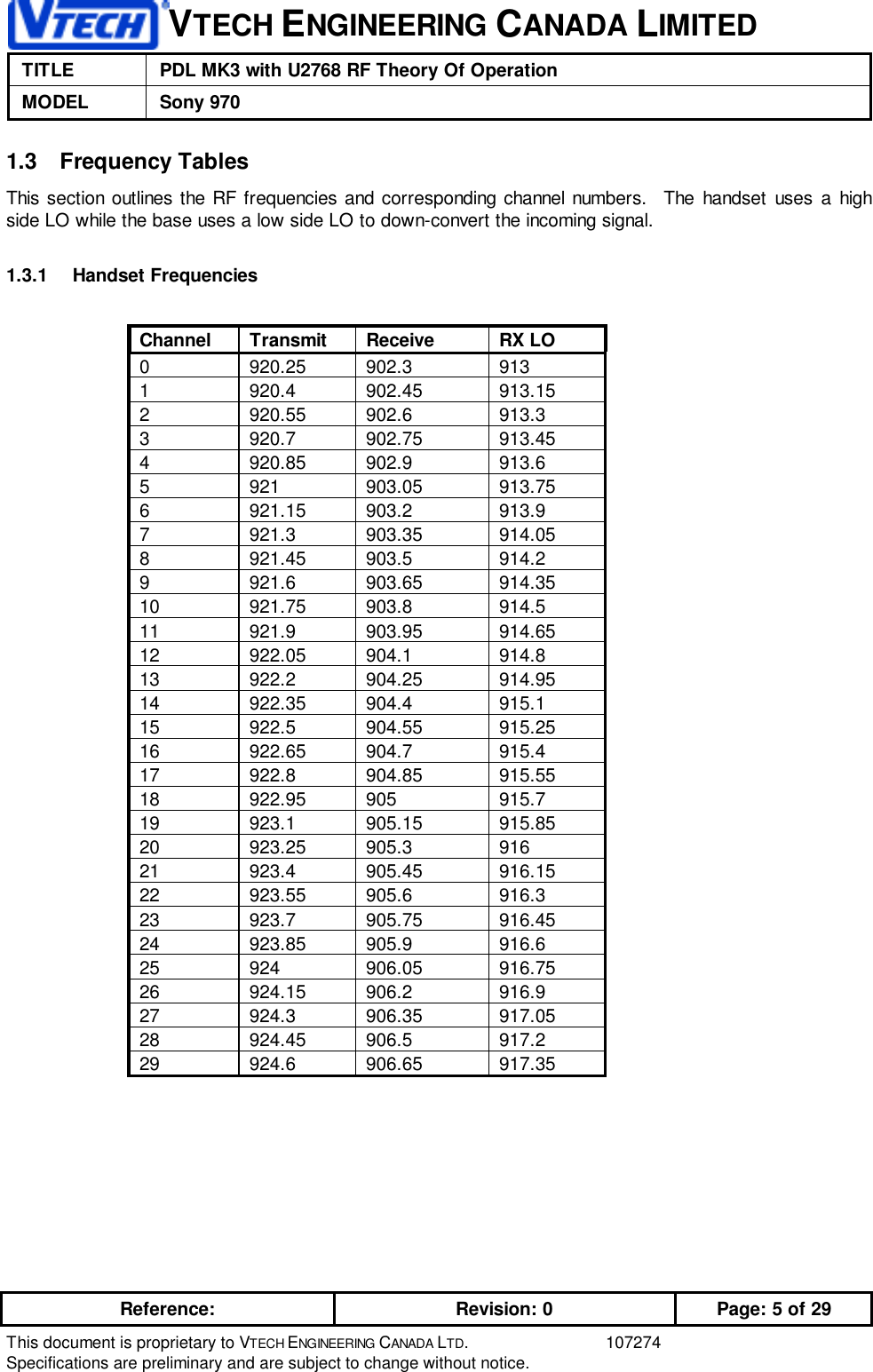
VTECH ENGINEERING CANADA LIMITEDTITLE PDL MK3 with U2768 RF Theory Of OperationMODEL Sony 970Reference: Revision: 0 Page: 5 of 29This document is proprietary to VTECH ENGINEERING CANADA LTD. 107274Specifications are preliminary and are subject to change without notice.1.3 Frequency TablesThis section outlines the RF frequencies and corresponding channel numbers.  The handset uses a highside LO while the base uses a low side LO to down-convert the incoming signal.1.3.1 Handset FrequenciesChannel Transmit Receive RX LO0 920.25 902.3 9131 920.4 902.45 913.152 920.55 902.6 913.33 920.7 902.75 913.454 920.85 902.9 913.65 921 903.05 913.756 921.15 903.2 913.97 921.3 903.35 914.058 921.45 903.5 914.29 921.6 903.65 914.3510 921.75 903.8 914.511 921.9 903.95 914.6512 922.05 904.1 914.813 922.2 904.25 914.9514 922.35 904.4 915.115 922.5 904.55 915.2516 922.65 904.7 915.417 922.8 904.85 915.5518 922.95 905 915.719 923.1 905.15 915.8520 923.25 905.3 91621 923.4 905.45 916.1522 923.55 905.6 916.323 923.7 905.75 916.4524 923.85 905.9 916.625 924 906.05 916.7526 924.15 906.2 916.927 924.3 906.35 917.0528 924.45 906.5 917.229 924.6 906.65 917.35
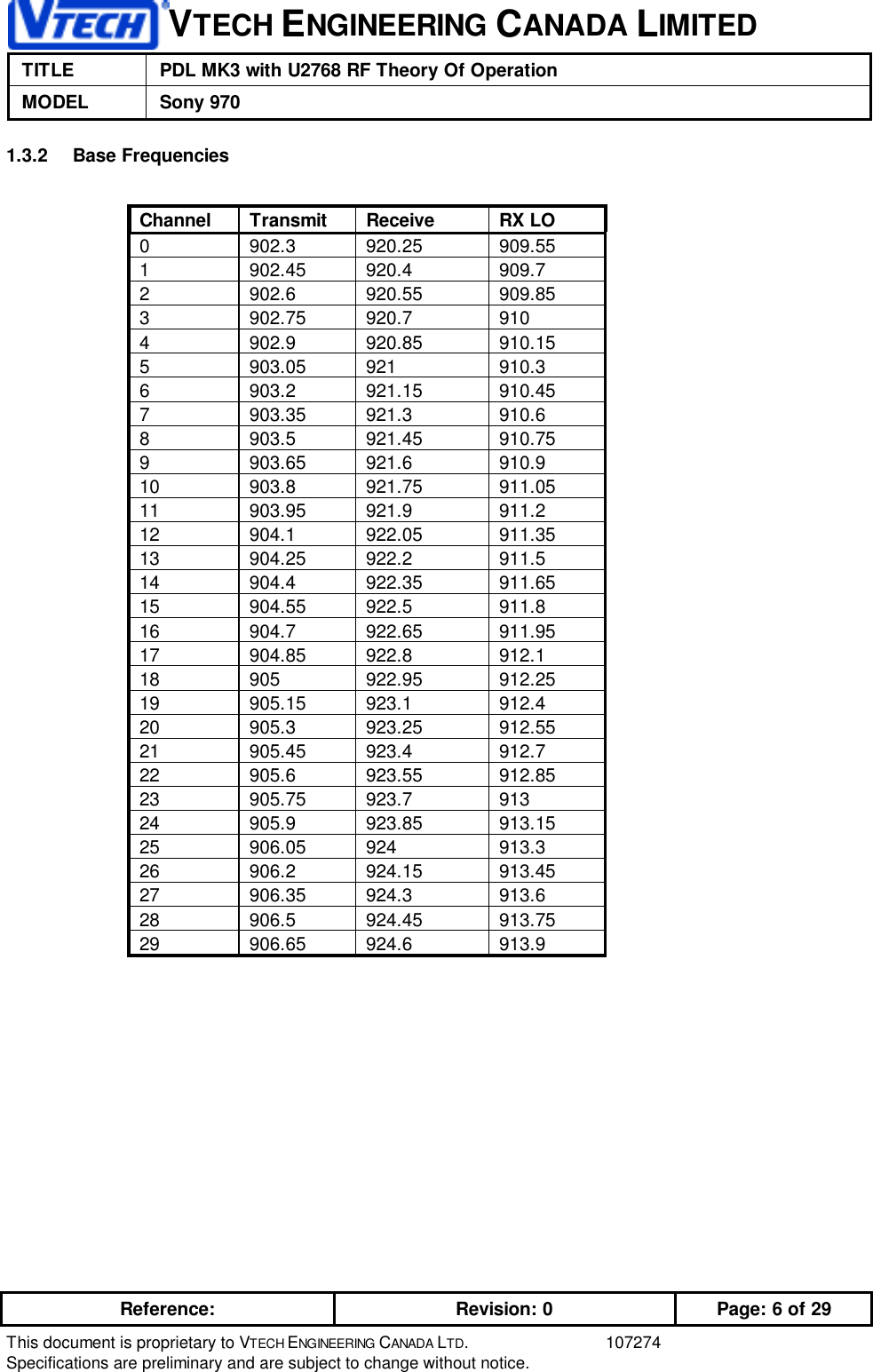
VTECH ENGINEERING CANADA LIMITEDTITLE PDL MK3 with U2768 RF Theory Of OperationMODEL Sony 970Reference: Revision: 0 Page: 6 of 29This document is proprietary to VTECH ENGINEERING CANADA LTD. 107274Specifications are preliminary and are subject to change without notice.1.3.2 Base FrequenciesChannel Transmit Receive RX LO0 902.3 920.25 909.551 902.45 920.4 909.72 902.6 920.55 909.853 902.75 920.7 9104 902.9 920.85 910.155 903.05 921 910.36 903.2 921.15 910.457 903.35 921.3 910.68 903.5 921.45 910.759 903.65 921.6 910.910 903.8 921.75 911.0511 903.95 921.9 911.212 904.1 922.05 911.3513 904.25 922.2 911.514 904.4 922.35 911.6515 904.55 922.5 911.816 904.7 922.65 911.9517 904.85 922.8 912.118 905 922.95 912.2519 905.15 923.1 912.420 905.3 923.25 912.5521 905.45 923.4 912.722 905.6 923.55 912.8523 905.75 923.7 91324 905.9 923.85 913.1525 906.05 924 913.326 906.2 924.15 913.4527 906.35 924.3 913.628 906.5 924.45 913.7529 906.65 924.6 913.9
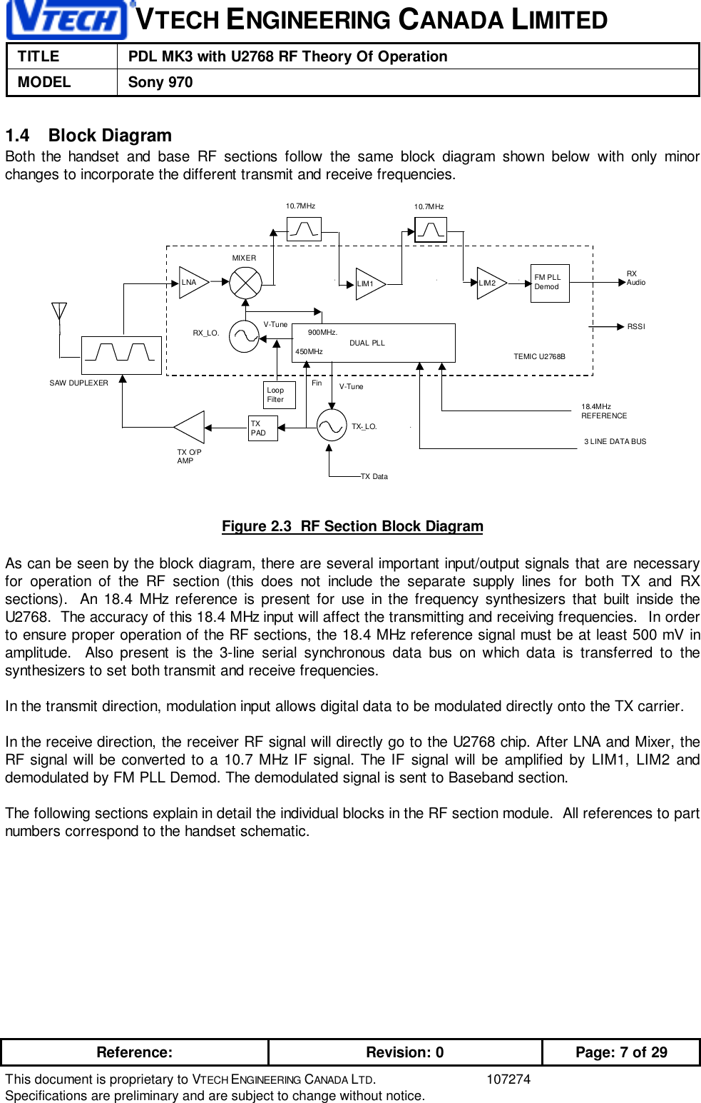
VTECH ENGINEERING CANADA LIMITEDTITLE PDL MK3 with U2768 RF Theory Of OperationMODEL Sony 970Reference: Revision: 0 Page: 7 of 29This document is proprietary to VTECH ENGINEERING CANADA LTD. 107274Specifications are preliminary and are subject to change without notice.1.4 Block DiagramBoth the handset and base RF sections follow the same block diagram shown below with only minorchanges to incorporate the different transmit and receive frequencies.18.4MHzREFERENCE3 LINE DATA BUSRX_LO.FinV-TuneTX O/PAMPTEMIC U2768BTX DataSAW DUPLEXERRXAudioRSSIDUAL PLLLNAMIXERV-TuneFM PLLDemodLIM2LIM110.7MHz10.7MHzLoopFilterTX_LO.450MHz900MHz.TXPADFigure 2.3  RF Section Block DiagramAs can be seen by the block diagram, there are several important input/output signals that are necessaryfor operation of the RF section (this does not include the separate supply lines for both TX and RXsections).  An 18.4 MHz reference is present for use in the frequency synthesizers that built inside theU2768.  The accuracy of this 18.4 MHz input will affect the transmitting and receiving frequencies.  In orderto ensure proper operation of the RF sections, the 18.4 MHz reference signal must be at least 500 mV inamplitude.  Also present is the 3-line serial synchronous data bus on which data is transferred to thesynthesizers to set both transmit and receive frequencies.In the transmit direction, modulation input allows digital data to be modulated directly onto the TX carrier.In the receive direction, the receiver RF signal will directly go to the U2768 chip. After LNA and Mixer, theRF signal will be converted to a 10.7 MHz IF signal. The IF signal will be amplified by LIM1, LIM2 anddemodulated by FM PLL Demod. The demodulated signal is sent to Baseband section.The following sections explain in detail the individual blocks in the RF section module.  All references to partnumbers correspond to the handset schematic.
VTECH ENGINEERING CANADA LIMITEDTITLE PDL MK3 with U2768 RF Theory Of OperationMODEL Sony 970Reference: Revision: 0 Page: 8 of 29This document is proprietary to VTECH ENGINEERING CANADA LTD. 107274Specifications are preliminary and are subject to change without notice.2  RF Section Detailed Operation2.1 Antenna Section2.1.1 AntennaThe antenna is a device that allows effective conversion of energy from air to the RF circuitry.  Theantennas used are a retractable 1/2 wave with 2.5 dB gain relative to an isotropic radiator and a fixed 1/4wave antenna with roughly 0 dB gain relative to an isotropic radiator.  The duplexer and filters that followthe antenna, require a 50 ohm match to operate properly.  The antenna is roughly matched to 50 ohms andrequires a simple microstrip matching network to achieve this.  If a network analyzer is attached to theBFA connector after disconnecting the duplexer, the antenna match may be measured.  In order to achievea good 50 ohm match, one must be careful not to obstruct the antenna as any object near the antenna willaffect its impedance.2.1.2 SAW DuplexerThe SAW Duplexer consists of two bandpass filters to provide the necessary isolation between transmitand receive sections and to pass the correct frequencies to transmit and receive sections.  To ensure thatthe Duplexer is operating correctly, the match looking into the filters from the BFA connector may bemeasured.  To do this it is necessary to remove the 0-ohm resistor that connects the antenna to theDuplexer.  A return loss of approximately 15 dB should be measured for both the TX and RX bands.2.2 Receive Section2.2.1 LNAU2768 first stage is LNA. The purpose of the LNA is to provide enough gain at a low noise figure so thatthe receiver can pick up the signal correctly.  It must provide a good 50 Ω match to the RX bandpass filter.2.2.2 RX MixerThe second stage of the U2768 is Mixer. The function of the mixer is to combine the incoming signal with aLO signal in order to convert the desired signal to the 10.7 MHz IF frequency.  The mixer output isconnected by 4:1 transformer, which has balance inputs and single output. The transformer outputconnects to 10.7MHz ceramic filter. This ceramic filter has 330 ohm input and output impedance and itsbandwidth 150 kHz.2.2.3 RX VCOThe RX VCO is provided by U2768 chip. This VCO oscillate at frequency 870-970MHz. This VCO outputinternally connects to U2768 PLL while its loop filter should be connected externally.2.2.4 RX SynthesizerThe U2768 also has Dual PLL for both the TX and RX sides.  The Synthesizers receive channel informationfrom the embedded microprocessor in the AMD ASIC via the serial buss.  It also requires a stable 18.4MHz reference clock that is also supplied by the AMD ASIC.
VTECH ENGINEERING CANADA LIMITEDTITLE PDL MK3 with U2768 RF Theory Of OperationMODEL Sony 970Reference: Revision: 0 Page: 9 of 29This document is proprietary to VTECH ENGINEERING CANADA LTD. 107274Specifications are preliminary and are subject to change without notice.A passive loop filter is employed to connect the synthesizer of the internal VCO.  This tuning voltage maybe observed from test point RX_LOOP_V on the bottom side of the PCB.  The loop filter cutoff frequencyis set to about 1 kHz to allow relatively fast power-up times (<15ms).2.2.5  IF Amplifier StageThere are two stages of IF amplification in the U2768, namely LIM1and LIM2. LIM1 and LIM2 provide theenough gain for the signal. Both of the LIM1 and LIM2 require external 10.7 MHz ceramic IF filters.2.2.6 IF FilteringThe choice of 10.7 MHz as an IF frequency, allows the use of relatively inexpensive filters.  Two ceramicfilters are used to achieve the desired adjacent channel suppression.  Two different bandwidth filters areused, 230 kHz and 150 kHz, so that any shifting in the passband does not narrow the bandwidthexcessively.2.2.7 DemodulatorThe U2768 contains FM PLL Demod.  This demodulator will demodulate the FM signal to the analog signaland this analog signal is sent to the baseband. The quadrature voltage can also be observed at the ATEtest point connector.  This voltage should nominally be 1.5 V for both the base and handset when a signalis center tuned.2.2.7.1 RSSI ComparatorThe U2768 provides an RSSI voltage that is proportional to the input signal level that is then sent to theASIC A/D pin.2.3 Transmit Section2.3.1 TX AmpThere is one transistor which provide the necessary gain for the transmit section.  Transistor Q3 amplifiesthe signal from the TX VCO. The output power is set through TX PAD (attenuation pad) such that weguarantee less then 50mV/meter radiated field strength measured at 3 meters.2.3.2 TX VCOTX VCO oscillates at 450MHz and the transistor Q1 output circuitry resonates at 2nd harmonic, which is theTX frequency. The TX VCO is also FSK modulated by the transmit data through a second varactor in thetank (25kHz peak).  The data to be modulated is first filtered and then the amplitude is set via a precisionresistor divider (R42/R46 both on handset and base) to set the deviation of the data modulation.2.3.3 TX Synthesizer/PLLThe TX PLL is also provided by U2768.  The TX frequency synthesizer is working at 450MHz. The loopfilter cutoff frequency is about 100 Hz.  This allows the data modulation to include frequencies down toabout 100 Hz.  The power-up time of the TX PLL is not critical (<60ms).

Navigation menu