VTech Telecommunications 80-4258-05 SPP-ID970 Cordless Telephone User Manual PDL MK3 Theory of Operation
VTech Telecommunications Ltd SPP-ID970 Cordless Telephone PDL MK3 Theory of Operation
Contents
- 1. RF Module Theory of Operation
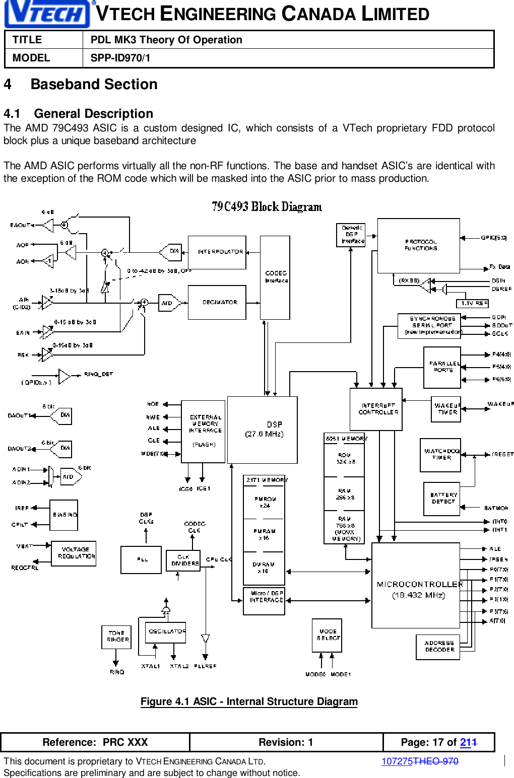
- 2. PDL MK3 Theory of Operation
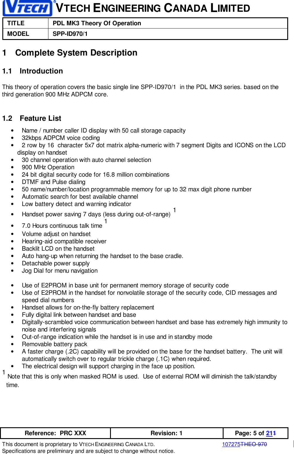
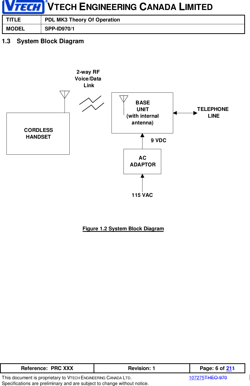
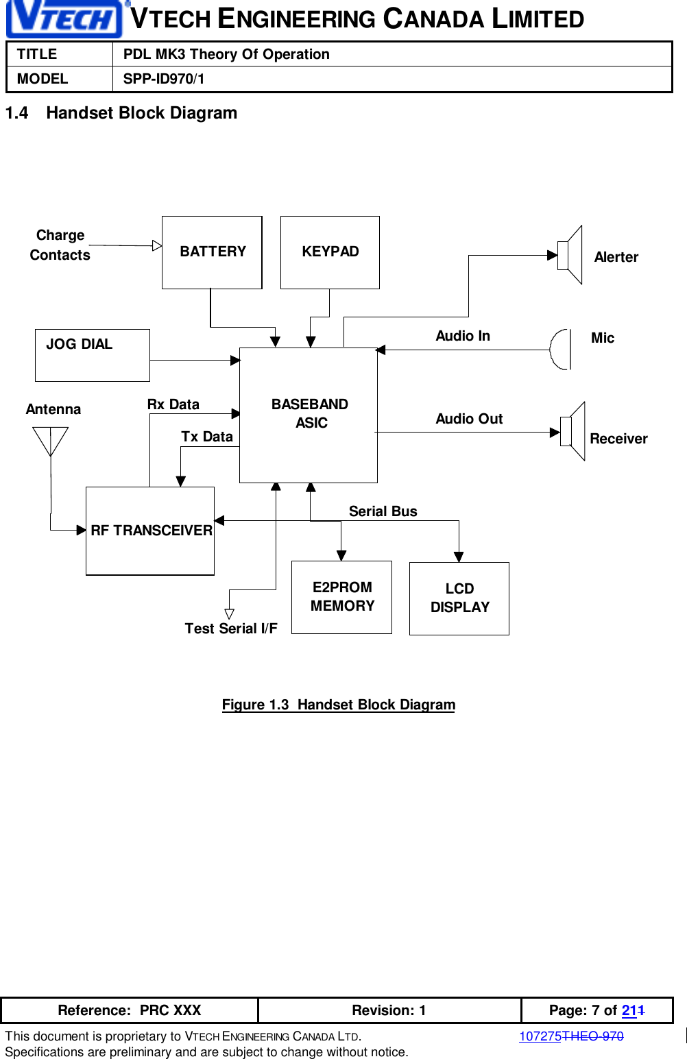
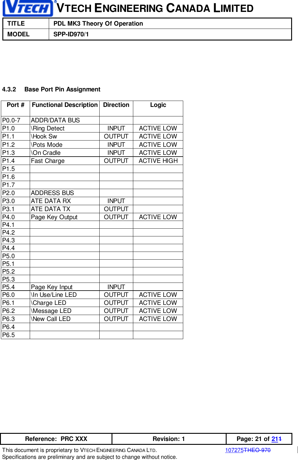
PDL MK3 Theory of Operation