VTech Telecommunications 80-4258-05 SPP-ID970 Cordless Telephone User Manual PDL MK3 Theory of Operation
VTech Telecommunications Ltd SPP-ID970 Cordless Telephone PDL MK3 Theory of Operation
Contents
- 1. RF Module Theory of Operation
- 2. PDL MK3 Theory of Operation
PDL MK3 Theory of Operation
VTECH ENGINEERING CANADA LIMITED
TITLE PDL MK3 Theory Of Operation
MODEL SPP-ID970/1
Reference: PRC XXX Revision: 1 Page: 1 of 211
This document is proprietary to VTECH ENGINEERING CANADA LTD.107275THEO-970
Specifications are preliminary and are subject to change without notice.
PDL MK3
THEORY OF OPERATION
for SONY
SPP-ID970/1
Document ID: THEO-970
PRC #: XXXX
Note: All rights reserved. No part of this publication may be reproduced or transmitted in any form or by
any means. The only controlled copy of this document is kept in electronic form on the VTECH computer
network. All printed copies are uncontrolled documents and are not updated. This Procedure is the
property of VTECH Engineering Canada Ltd., and shall be returned upon request
.
Prepared By Guy Pothiboon
Title Project Manager
Approved By
Title
VTECH ENGINEERING CANADA LIMITED
TITLE PDL MK3 Theory Of Operation
MODEL SPP-ID970/1
Reference: PRC XXX Revision: 1 Page: 2 of 211
This document is proprietary to VTECH ENGINEERING CANADA LTD.107275THEO-970
Specifications are preliminary and are subject to change without notice.
Revision History
Revision No Description Page Effective Date
1 Initial Release All 19-Feb-99

VTECH ENGINEERING CANADA LIMITED
TITLE PDL MK3 Theory Of Operation
MODEL SPP-ID970/1
Reference: PRC XXX Revision: 1 Page: 3 of 211
This document is proprietary to VTECH ENGINEERING CANADA LTD.107275THEO-970
Specifications are preliminary and are subject to change without notice.
Table of Contents
1 Complete System Description................................................ 5
1.1 Introduction............................................................................................ 5
1.2 Feature List............................................................................................. 5
1.3 System Block Diagram........................................................................... 6
1.4 Handset Block Diagram.......................................................................... 7
1.5 Base Block Diagram ............................................................................... 8
2 RF Section Overview............................................................... 9
2.1 Introduction............................................................................................ 9
2.2 Frequency Tables................................................................................... 10
2.2.1 Handset Frequencies.................................................................................................. 10
2.2.2 Base Frequencies....................................................................................................... 11
2.3 Block Diagram........................................................................................ 12
3 RF Section Detailed Operation............................................... 13
3.1 Antenna Section..................................................................................... 13
3.1.1 Antenna...................................................................................................................... 13
3.1.2 SAW Duplexer ............................................................................................................ 13
3.2 Receive Section...................................................................................... 13
3.2.1 RX Amps and SAW Filter ............................................................................................ 13
3.2.2 RX Mixer..................................................................................................................... 14
3.2.3 RX VCO and LO Buffer............................................................................................... 14
3.2.4 RX Synthesizer........................................................................................................... 15
3.2.5 IF Amplifier Stage....................................................................................................... 15
3.2.6 IF Filtering.................................................................................................................. 15
3.2.7 Mixer, IF Amplifier, FM Demodulator (Temic IC).......................................................... 15
3.3 Transmit Section .................................................................................... 16
3.3.1 TX Amp....................................................................................................................... 16
3.3.2 TX VCO ...................................................................................................................... 16
3.3.3 TX Synthesizer/PLL.................................................................................................... 16

VTECH ENGINEERING CANADA LIMITED
TITLE PDL MK3 Theory Of Operation
MODEL SPP-ID970/1
Reference: PRC XXX Revision: 1 Page: 4 of 211
This document is proprietary to VTECH ENGINEERING CANADA LTD.107275THEO-970
Specifications are preliminary and are subject to change without notice.
4 Baseband Section ................................................................... 17
4.1 General Description ............................................................................... 17
4.2 Detailed Functional Description ............................................................ 18
4.2.1 Protocol Functions..................................................................................................... 18
4.2.2 Audio Functions ......................................................................................................... 18
4.2.3 System Control Functions.......................................................................................... 18
4.3 Port Pin Assignment And Functions..................................................... 20
4.3.1 Handset Port Pin Assignment..................................................................................... 20
4.3.2 Base Port Pin Assignment.......................................................................................... 21

VTECH ENGINEERING CANADA LIMITED
TITLE PDL MK3 Theory Of Operation
MODEL SPP-ID970/1
Reference: PRC XXX Revision: 1 Page: 5 of 211
This document is proprietary to VTECH ENGINEERING CANADA LTD.107275THEO-970
Specifications are preliminary and are subject to change without notice.
1 Complete System Description
1.1 Introduction
This theory of operation covers the basic single line SPP-ID970/1 in the PDL MK3 series. based on the
third generation 900 MHz ADPCM core.
1.2 Feature List
• Name / number caller ID display with 50 call storage capacity
• 32kbps ADPCM voice coding
• 2 row by 16 character 5x7 dot matrix alpha-numeric with 7 segment Digits and ICONS on the LCD
display on handset
• 30 channel operation with auto channel selection
• 900 MHz Operation
• 24 bit digital security code for 16.8 million combinations
• DTMF and Pulse dialing
• 50 name/number/location programmable memory for up to 32 max digit phone number
• Automatic search for best available channel
• Low battery detect and warning indicator
• Handset power saving 7 days (less during out-of-range) 1
• 7.0 Hours continuous talk time 1
• Volume adjust on handset
• Hearing-aid compatible receiver
• Backlit LCD on the handset
• Auto hang-up when returning the handset to the base cradle.
• Detachable power supply
• Jog Dial for menu navigation
• Use of E2PROM in base unit for permanent memory storage of security code
• Use of E2PROM in the handset for nonvolatile storage of the security code, CID messages and
speed dial numbers
• Handset allows for on-the-fly battery replacement
• Fully digital link between handset and base
• Digitally-scrambled voice communication between handset and base has extremely high immunity to
noise and interfering signals
• Out-of-range indication while the handset is in use and in standby mode
• Removable battery pack
• A faster charge (.2C) capability will be provided on the base for the handset battery. The unit will
automatically switch over to regular trickle charge (.1C) when required.
• The electrical design will support charging in the face up position.
1 Note that this is only when masked ROM is used. Use of external ROM will diminish the talk/standby
time.
VTECH ENGINEERING CANADA LIMITED
TITLE PDL MK3 Theory Of Operation
MODEL SPP-ID970/1
Reference: PRC XXX Revision: 1 Page: 6 of 211
This document is proprietary to VTECH ENGINEERING CANADA LTD.107275THEO-970
Specifications are preliminary and are subject to change without notice.
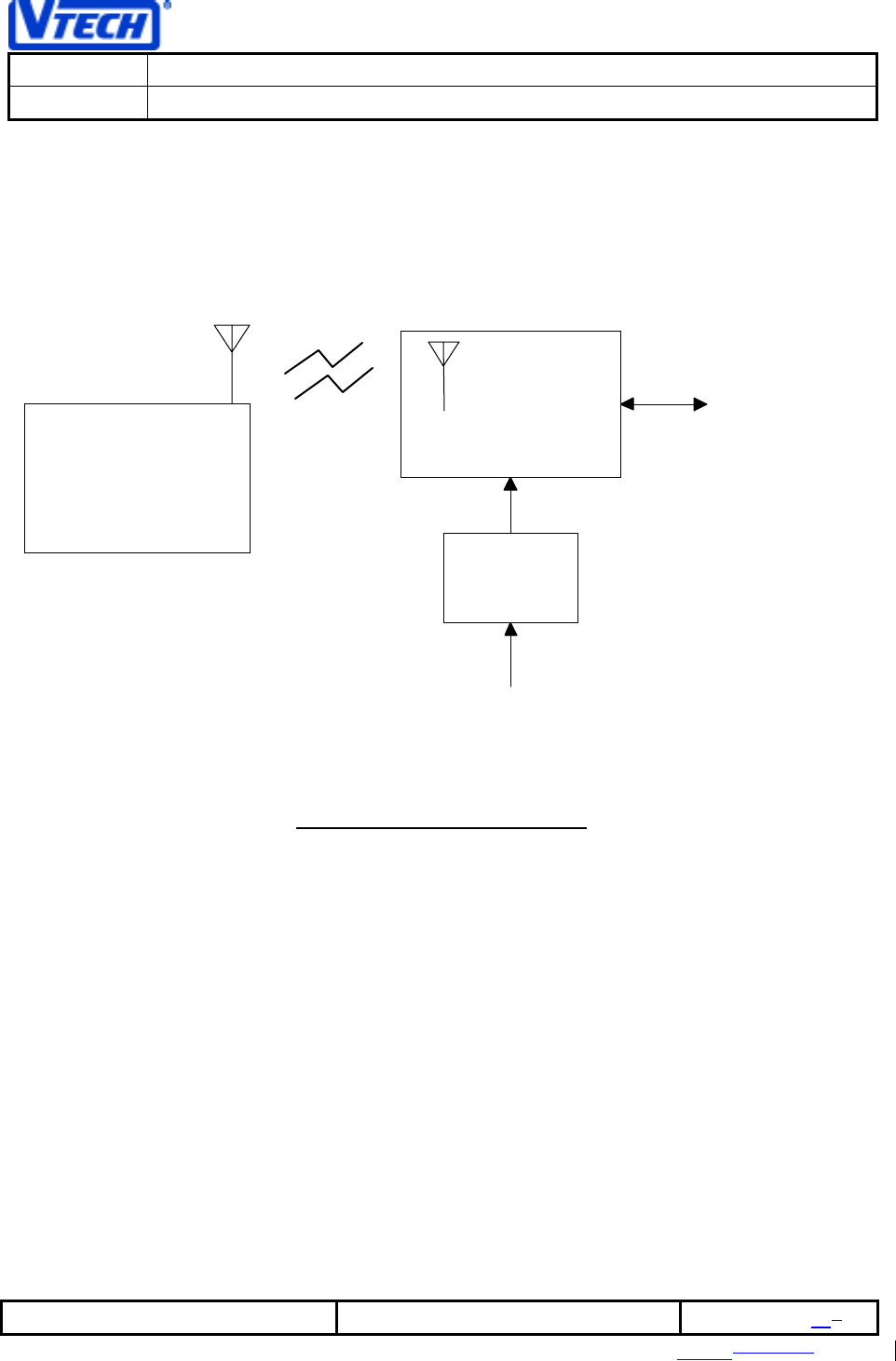
1.3 System Block Diagram
Figure 1.2 System Block Diagram
CORDLESS
HANDSET
BASE
UNIT
(with internal
antenna)
AC
ADAPTOR
115 VAC
TELEPHONE
LINE
2-way RF
Voice/Data
Link
9 VDC
VTECH ENGINEERING CANADA LIMITED
TITLE PDL MK3 Theory Of Operation
MODEL SPP-ID970/1
Reference: PRC XXX Revision: 1 Page: 7 of 211
This document is proprietary to VTECH ENGINEERING CANADA LTD.107275THEO-970
Specifications are preliminary and are subject to change without notice.
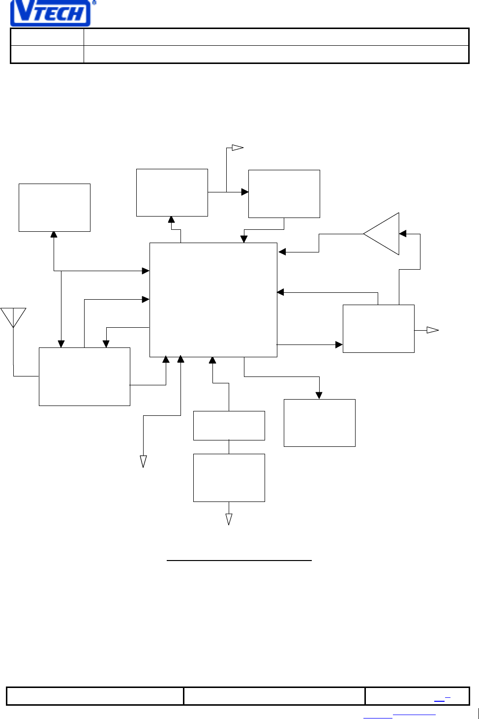
1.4 Handset Block Diagram
Figure 1.3 Handset Block Diagram
BASEBAND
ASIC
RF TRANSCEIVER
KEYPAD
Antenna
Tx Data
Rx Data
Test Serial I/F
E2PROM
MEMORY
BATTERY
LCD
DISPLAY
Receiver
Audio In Mic
Audio Out
Charge
Contacts
Serial Bus
Alerter
JOG DIAL
VTECH ENGINEERING CANADA LIMITED
TITLE PDL MK3 Theory Of Operation
MODEL SPP-ID970/1
Reference: PRC XXX Revision: 1 Page: 8 of 211
This document is proprietary to VTECH ENGINEERING CANADA LTD.107275THEO-970
Specifications are preliminary and are subject to change without notice.
1.5 Base Block Diagram
Figure 1.4 Base Block Diagram
BASEBAND
ASIC
RF TRANSCEIVER
E2PROM
MEMORY
SPARE
BATTERY
Antenna
Serial Bus
Tx Data
Rx Data
Test Serial I/F
TELEPHONE
LINE
INTERFACE
Rx Audio
Tx Audio Tel Line
AC
ADAPTOR
115 VAC
BATTERY
CHARGER
Cradle Charge
Contacts
LED
DISPLAY
CID
FSKSignals
RSSI
CID
AMP
VOLT REG
Reg
Ctrl

VTECH ENGINEERING CANADA LIMITED
TITLE PDL MK3 Theory Of Operation
MODEL SPP-ID970/1
Reference: PRC XXX Revision: 1 Page: 9 of 211
This document is proprietary to VTECH ENGINEERING CANADA LTD.107275THEO-970
Specifications are preliminary and are subject to change without notice.
2 RF Section Overview
2.1 Introduction
The basic function of the base and handset RF sections is to provide a full duplex wireless link between the
handset and base sections of the telephone. This is accomplished by setting up two simultaneous
communications links between the handset and base RF boards. The RF receiver and transmitter circuitry
essentially provide a link between the microphone and receiver in the handset to the telephone line in the
base set. In this way the phone performs exactly as a corded phone, except without the cord.
The frequency at which the handset transmits to the base is centered around 926.55 MHz, and the
frequency at which the base transmits to the handset is centered around 903.8 MHz. The data rate which
is modulated onto the RF carrier is 48 kbps. On the receiver side, the data is extracted and then
converted back into the original audio signal.
It is important to note that the synthesizer / pre-scaler IC only operates up to 500 MHz. The VCO's
therefore oscillate at roughly 450 MHz. The 900 MHz signals needed for the transmit and receive sections
are generated from the second harmonic of the VCO frequencies.
The following section will outline the transmit frequencies used as well as the corresponding LO frequency
which is used for the receiver. This is followed by the Block diagram and a block by block functional
description of the modules.
VTECH ENGINEERING CANADA LIMITED
TITLE PDL MK3 Theory Of Operation
MODEL SPP-ID970/1
Reference: PRC XXX Revision: 1 Page: 10 of 211
This document is proprietary to VTECH ENGINEERING CANADA LTD.107275THEO-970
Specifications are preliminary and are subject to change without notice.
2.2 Frequency Tables
This section outlines the RF frequencies and corresponding channel numbers. The handset uses a high
side LO while the base uses a low side LO to down-convert the incoming signal.
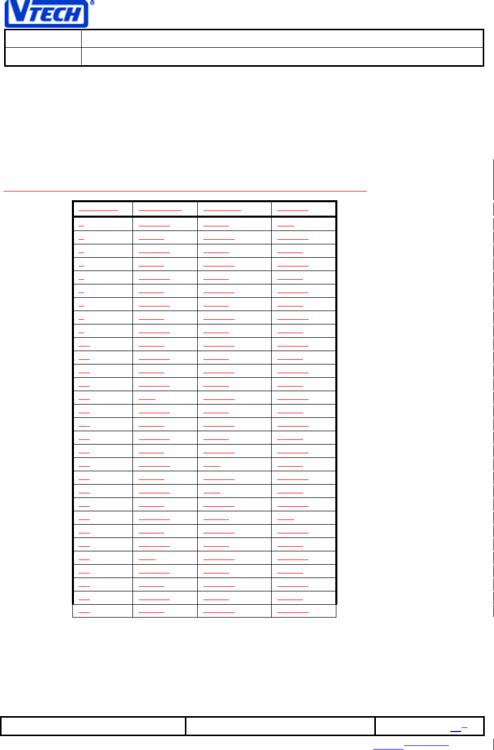
2.2.1 Handset Frequencies
Please refer to the new Handset Freq. table shown in file “MK3_68_RF_OP.doc”
Channel Transmit Receive RX LO
1925.05 902.3 913
2925.2 902.45 913.15
3925.35 902.6 913.3
4925.5 902.75 913.45
5925.65 902.9 913.6
6925.8 903.05 913.75
7925.95 903.2 913.9
8926.1 903.35 914.05
9926.25 903.5 914.2
10 926.4 903.65 914.35
11 926.55 903.8 914.5
12 926.7 903.95 914.65
13 926.85 904.1 914.8
14 927 904.25 914.95
15 927.15 904.4 915.1
16 927.3 904.55 915.25
17 927.45 904.7 915.4
18 927.6 904.85 915.55
19 927.75 905 915.7
20 923.1 904.85 915.55
21 923.25 905 915.7
22 923.4 905.15 915.85
23 923.55 905.3 916
24 923.7 905.45 916.15
25 923.85 905.6 916.3
26 924 905.75 916.45
27 924.15 905.9 916.6
28 924.3 906.05 916.75
29 924.45 906.2 916.9
30 924.6 906.35 917.05
VTECH ENGINEERING CANADA LIMITED
TITLE PDL MK3 Theory Of Operation
MODEL SPP-ID970/1
Reference: PRC XXX Revision: 1 Page: 11 of 211
This document is proprietary to VTECH ENGINEERING CANADA LTD.107275THEO-970
Specifications are preliminary and are subject to change without notice.
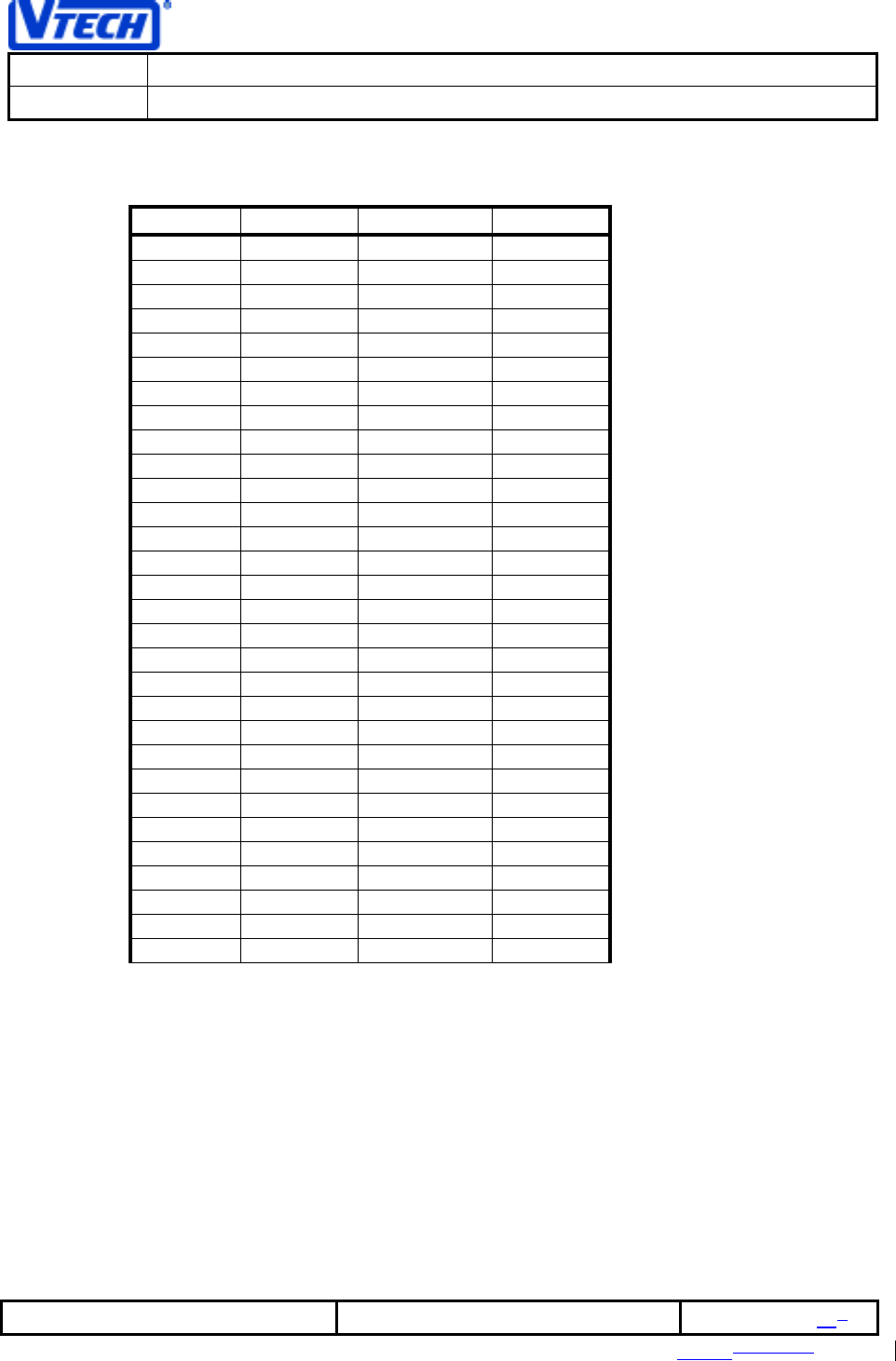
2.2.2 Base Frequencies
Channel Transmit Receive RX LO
1 902.3 925.05 914.35
2 902.45 925.2 914.5
3 902.6 925.35 914.65
4 902.75 925.5 914.8
5 902.9 925.65 914.95
6 903.05 925.8 915.1
7 903.2 925.95 915.25
8 903.35 926.1 915.4
9 903.5 926.25 915.55
10 903.65 926.4 915.7
11 903.8 926.55 915.85
12 903.95 926.7 916
13 904.1 926.85 916.15
14 904.25 927 916.3
15 904.4 927.15 916.45
16 904.55 927.3 916.6
17 904.7 927.45 916.75
18 904.85 927.6 916.9
19 905 927.75 917.05
20 905.15 923.1 912.4
21 905.3 923.25 912.55
22 905.45 923.4 912.7
23 905.6 923.55 912.85
24 905.75 923.7 913
25 905.9 923.85 913.15
26 906.05 924 913.3
27 906.2 924.15 913.45
28 906.35 924.3 913.6
29 906.5 924.45 913.75
30 906.65 924.6 913.9
VTECH ENGINEERING CANADA LIMITED
TITLE PDL MK3 Theory Of Operation
MODEL SPP-ID970/1
Reference: PRC XXX Revision: 1 Page: 12 of 211
This document is proprietary to VTECH ENGINEERING CANADA LTD.107275THEO-970
Specifications are preliminary and are subject to change without notice.
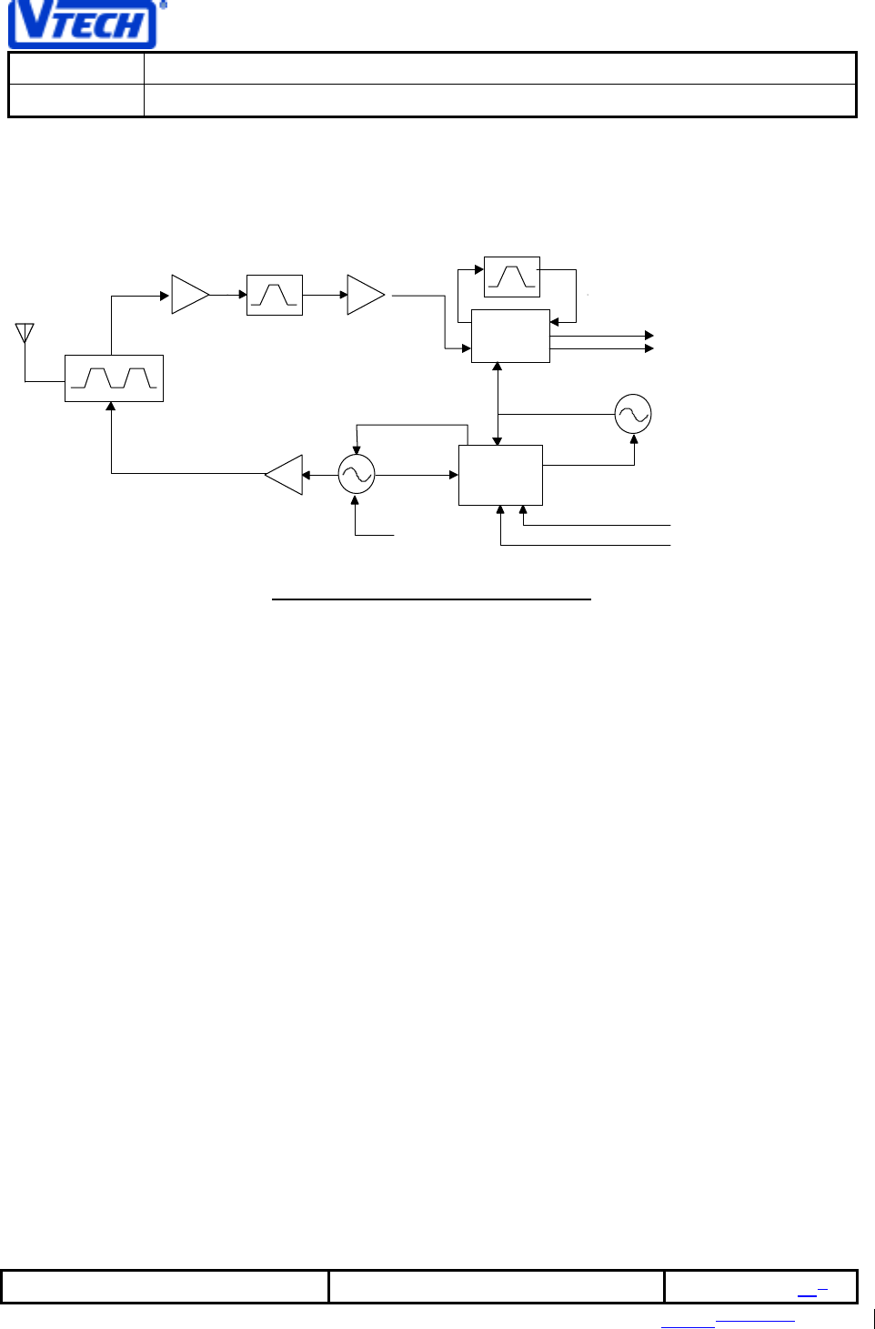
2.3 Block Diagram
Both the handset and base RF sections follow the same block diagram shown below with only minor
changes to incorporate the different transmit and receive frequencies.
SAW
FILTER
SYNTHESIZER
18.25 MHz
REFERENCE
3 LINE DATA BUS
RX L.O.
DUAL
PRESCALER/
457
MHz
Fin
Fin V-tune
V-Tune
2nd RX
AMP
(Base only)
IF AMP,
MIXER
DEMOD
1st RX
AMP
TX O/P
A
MP
TEMIC U2765B
TX Data
SAW DUPLEXER
RX
Audio
10.7 MHz
Ceramics
RSSI
Figure 2.3 RF Section Block Diagram
As can be seen by the block diagram, there are several important input/output signals which are necessary
for operation of the RF section (this does not include the separate supply lines for both TX and RX
sections). An 18.25 MHz reference is present for use in the frequency synthesizers. The accuracy of this
18.25 MHz input will affect the transmit and receive frequencies. In order to ensure proper operation of
the RF sections, the 18.25 MHz reference signal must be at least 500 mV in amplitude. Also present is the
3-line serial synchronous data bus on which data is transferred to the synthesizers to set both the transmit
and receive frequencies.
In the transmit direction, modulation input allows digital data to be modulated directly onto the TX carrier.
In the receive direction, the RF section performs a single down-conversion of the incoming RF signal to
10.7 MHz where it is demodulated and sent to the AMD ASIC. The Data output is the demodulated signal
which is sent to the ASIC to be filtered and shaped by an internal data slicer. The reconstructed data
represents the original voice which is can then be processed by the DSP in the ASIC..
The following section explains the individual blocks in the RF section in detail. All reference to part
numbers correspond to the handset schematic.

VTECH ENGINEERING CANADA LIMITED
TITLE PDL MK3 Theory Of Operation
MODEL SPP-ID970/1
Reference: PRC XXX Revision: 1 Page: 13 of 211
This document is proprietary to VTECH ENGINEERING CANADA LTD.107275THEO-970
Specifications are preliminary and are subject to change without notice.
3 RF Section Detailed Operation
3.1 Antenna Section
3.1.1 Antenna
The antenna is a device which allows effective conversion of energy from air to the RF circuitry. The
antennas used are a retractable 1/2 wave with 2.5 dB gain relative to an isotropic radiator and a fixed 1/4
wave antenna with roughly 0 dB gain relative to an isotropic radiator. The duplexer and filters which follow
the antenna, require a 50 ohm match to operate properly. The antenna is roughly matched to 50 ohms and
requires a simple microstrip matching network to achieve this. If a network analyzer is attached to the
BFA connector after disconnecting the duplexer, the antenna match may be measured. In order to achieve
a good 50 ohm match, one must be careful not to obstruct the antenna as any object near the antenna will
affect its impedance.
3.1.2 SAW Duplexer
The SAW Duplexer consists of two bandpass filters to provide the necessary isolation between transmit
and receive sections and to pass the correct frequencies to transmit and receive sections. To ensure that
the Duplexer is operating correctly, the match looking into the filters from the BFA connector may be
measured. To do this it is necessary to remove the 0 ohm resistor which connects the antenna to the
Duplexer. A return loss of approximately 15 dB should be measured for both the TX and RX bands.
3.2 Receive Section
3.2.1 RX Amps and SAW Filter
The purpose of the first RX amp is to provide enough gain that the noise figure of the RX section is fixed to
as low a value as possible. It must provide a good 50 Ω match to both the RX bandpass filter and the
SAW filter. This amplifier must also have good power handling capability due to the limited filtering which
precedes it. The design employs a collector inductor to improve the output power capability of the
transistor. This form of matching also ensures that the gain of this stage is not too wide band further
improving its performance by allowing it to effectively reject signals which are far out of its passband.
Directly following the first RX amp is the SAW filter. This filter is responsible for the bulk of the filtering in
the receive section. It provides more than 40dB of image rejection and TX carrier suppression. The
insertion loss of this filter is relatively high due to its SAW implementation. It has an insertion loss of less
than 5 dB, typically 4 dB. An amplifier is required before this SAW filter to keep the noise figure low. If it
were not present, the noise figure of the phone would increase by the 4 dB loss associated with the SAW
filter.
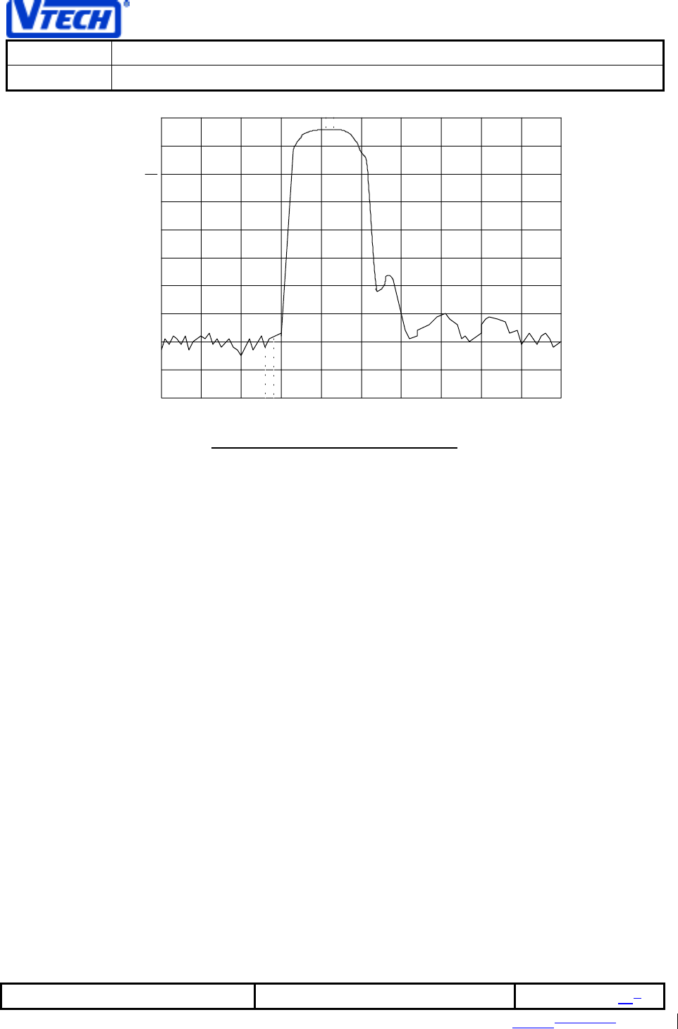
The second RX amp provides a limited amount of gain. Its main function is to ensure that the mixer sees a
good wideband match. Measuring the RX gain from the BFA connector to the output of this amplifier will
produce results as shown in Figure 4 below.
VTECH ENGINEERING CANADA LIMITED
TITLE PDL MK3 Theory Of Operation
MODEL SPP-ID970/1
Reference: PRC XXX Revision: 1 Page: 14 of 211
This document is proprietary to VTECH ENGINEERING CANADA LTD.107275THEO-970
Specifications are preliminary and are subject to change without notice.
0 dB
10 dB/div
875 975
925-928MHz Passband
902-905MHz Reject Band
Figure 3.2.1 RX Front End Response
3.2.2 RX Mixer
The function of the mixer is to combine the incoming signal with a LO signal in order to convert the desired
signal to the 10.7 MHz IF frequency. The mixer used for this task is a dual gate FET (NEC 25139). The
LO and RF signals are placed on the gates of the FET and the IF signal is coupled off of the drain. The
FET provides conversion gain along with adequate power handling characteristics. Both the RF and LO
ports are shorted to ground by spiral microstrip inductors on base unit and, spiral microstrip and SMT
inductors on the handset. These inductors provide a high impedance at both the RF and LO frequencies
while presenting a very low impedance at the IF frequency. The mixer is followed by an emitter follower
which converts the high impedance output of the mixer to a 330 ohm output suitable for directly driving the
IF ceramic filters. The gain for the pair (mixer and follower) is about 4 dB (50 ohms in, 330 ohms out).
3.2.3 RX VCO and LO Buffer
The RX VCO is a Colpitt's type oscillator operating at about 450 MHz with a frequency selective network
tuned to about 900 MHz on the collector. The frequency of oscillation is controlled by a varactor diode in
the tank circuit connected to the base of the transistor. This diode is connected to the loop voltage from
the RX synthesizer. Rough tuning is achieved with a variable chip cap. This capacitor is used to center the
tuning voltage to ensure reliable operation over a wide temperature range and also to compensate for
variances in component values.
The 450 MHz LO for the PLL is coupled off of the emitter of the VCO transistor. This is lightly coupled to
ensure that the VCO is not loaded by the PLL. The 900 MHz RX LO signal for the Mixer is coupled off the
collector of the VCO transistor.

VTECH ENGINEERING CANADA LIMITED
TITLE PDL MK3 Theory Of Operation
MODEL SPP-ID970/1
Reference: PRC XXX Revision: 1 Page: 15 of 211
This document is proprietary to VTECH ENGINEERING CANADA LTD.107275THEO-970
Specifications are preliminary and are subject to change without notice.
3.2.4 RX Synthesizer
The PLL and prescaler for both the TX and RX sides are now combined into one IC. The Synthesizer
receives channel information from the embedded microprocessor in the AMD ASIC via the serial buss. It
also requires a stable 18.25 MHz reference which is also supplied from the AMD ASIC.
A passive loop filter is employed to connect the synthesizer to the VCO. This tuning voltage may be
observed from test point RX_LOOP_V on the bottom side of the PCB. The loop filter cutoff frequency is
set to about 1 kHz to allow relatively fast power-up times.
3.2.5 IF Amplifier Stage
There is only one stage of discrete IF amplification. Transistor Q8 on the base (Q5 on handset) is used as
an amplifier with 330 ohms input and output impedance. The rest of the IF gain is provided by the FM
demod IC discussed below.
3.2.6 IF Filtering
The choice of 10.7 MHz as an IF frequency, allows the use of relatively inexpensive filters. Two ceramic
filters are used to achieve the desired adjacent channel suppression. Two different bandwidth filters are
used, 230 kHz and 150 kHz, so that any shifting in the passband does not narrow the bandwidth
excessively.
3.2.7 Mixer, IF Amplifier, FM Demodulator (Temic IC)
The RF design uses an integrated solution that provides a number of different receiver functions on a single
silicon chip. The Temic U2765B IC combines a, mixer down-converter, IF amplifier and FM demodulator
onto one device.
3.2.7.1 Rx Mixer
The function of the mixer is to combine the incoming signal with a LO signal in order to convert the desired
signal to the 10.7 MHz intermediate frequency (IF). The LO and RF signals are coupled onto pins 26 and
3 respectively on the Temic IC. The mixer output is coupled off of the Temic IC by a 10.7 MHz transformer
to a 10.7 MHz ceramic IF filter before it is injected into limiter 1 within the Temic IC. The output of limiter 1
is coupled off of the Temic IC into another 10.7 MHz ceramic IF filter.
3.2.7.2 IF Amplifier Stage
There is a two-stage limiting amplifier integrated with the Temic IC. Both of the limiters require external
10.7 MHz ceramic IF filters.
3.2.7.3 Demodulator
The quadrature circuit is made up one inductor, one resistor, and two capacitors. One of the two
capacitors is a variable capacitor that allows tuning of the circuit. The quadrature voltage may be
observed at the ATE test point connector. This voltage should nominally be 1.2 V for both the base and
handset when a signal is centre tuned.
The recovered audio signal from the demodulator has a peak-to-peak amplitude of approximately 0.31 V
(for 50 kHz peak-to-peak modulation). One path from the recovered audio port is filtered through a low-
pass data filter and passed back into the baseband module.

VTECH ENGINEERING CANADA LIMITED
TITLE PDL MK3 Theory Of Operation
MODEL SPP-ID970/1
Reference: PRC XXX Revision: 1 Page: 16 of 211
This document is proprietary to VTECH ENGINEERING CANADA LTD.107275THEO-970
Specifications are preliminary and are subject to change without notice.
3.2.7.4 RSSI Comparator
The U2765B provides an RSSI voltage that is proportional to the input signal level that is then sent to the
ASIC A/D pin.
3.3 Transmit Section
3.3.1 TX Amp
There is one transistor which provide the necessary gain for the transmit section. Transistor Q1 amplifies
the signal from the TX VCO. The output power is set such that we guarantee less then 50mV/meter
radiated field strength measured at 3 meters.
3.3.2 TX VCO
The basic operation of the TX VCO is the same as the RX VCO, except for one detail. The TX VCO is
also FSK modulated by the transmit data through a second varactor in the tank (25kHz peak to peak). The
data is first filtered and then the amplitude is set via a precision resistor divider (R119/R120 on handset
and R27/R179 on base) to set the deviation of the data modulation.
3.3.3 TX Synthesizer/PLL
The TX PLL is combined into one IC with the RX PLL. See above. The loop filter cutoff frequency is
about 100 Hz. This allows the data modulation to include frequencies down to about 100 Hz. The power-
up time of the TX PLL is not critical.
VTECH ENGINEERING CANADA LIMITED
TITLE PDL MK3 Theory Of Operation
MODEL SPP-ID970/1
Reference: PRC XXX Revision: 1 Page: 17 of 211
This document is proprietary to VTECH ENGINEERING CANADA LTD.107275THEO-970
Specifications are preliminary and are subject to change without notice.
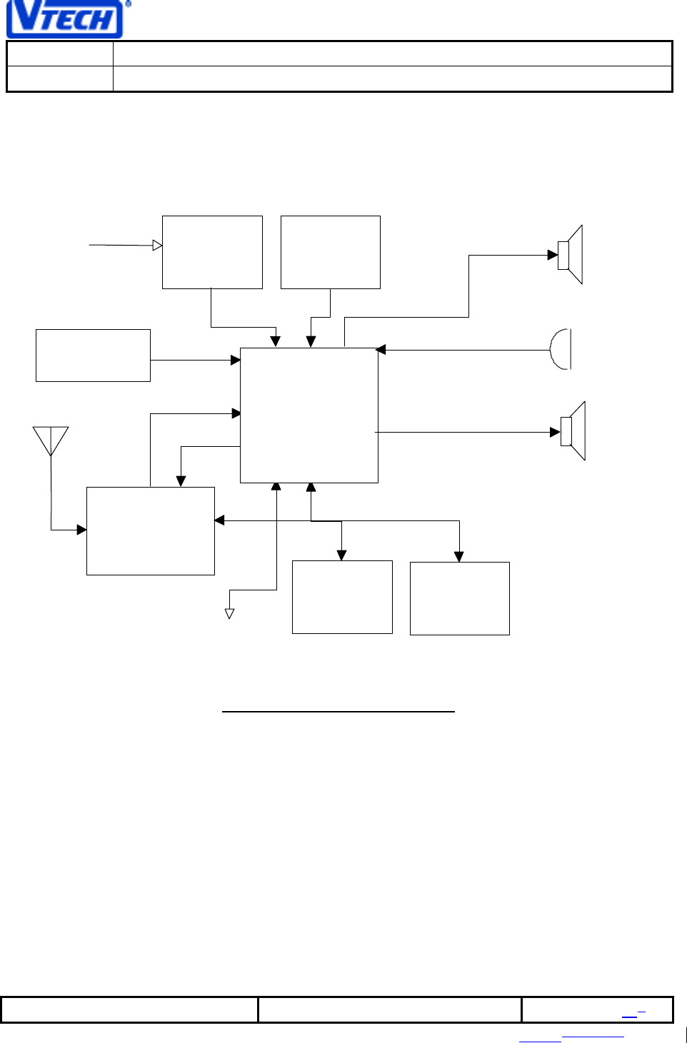
4 Baseband Section
4.1 General Description
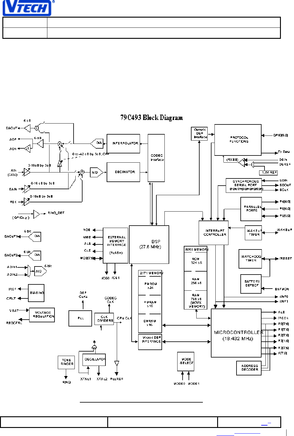
The AMD 79C493 ASIC is a custom designed IC, which consists of a VTech proprietary FDD protocol
block plus a unique baseband architecture
The AMD ASIC performs virtually all the non-RF functions. The base and handset ASIC’s are identical with
the exception of the ROM code which will be masked into the ASIC prior to mass production.
Figure 4.1 ASIC - Internal Structure Diagram

VTECH ENGINEERING CANADA LIMITED
TITLE PDL MK3 Theory Of Operation
MODEL SPP-ID970/1
Reference: PRC XXX Revision: 1 Page: 18 of 211
This document is proprietary to VTECH ENGINEERING CANADA LTD.107275THEO-970
Specifications are preliminary and are subject to change without notice.
4.2 Detailed Functional Description
The principle components are:
4.2.1 Protocol Functions
The protocol block conducts a signaling and a voice channel in the transmit and receive directions. All data
I/O are CMOS levels.
4.2.2 Audio Functions
1) CODEC. The CODEC transcodes analog voice signals and 32 kbps ADPCM data.
2) Audio Front End. The audio front end connects the analog voice I/O pins to the CODEC.
3) Tone Ringer. The tone ringer produces amplitude controllable square-wave ringing tone signals for
output on the RING pin.
4) Biasing. The biasing circuits establish precision currents and voltage references to support audio
and battery detection analog operations.
5) DTMF Generator. The DTMF generator produces digitally-generated tones for DTMF dialing and
call progress tones.
4.2.3 System Control Functions
1. Microcontroller: An 8-bit 80C32T2 microcontroller executes the program and controls the
protocol logic and other hardware configuration. It includes 32 Kbytes of mask-programmable
ROM and a total of 1K bytes of RAM. It also includes an asynchronous serial port.
2. Synchronous Serial Port: The serial port provides a synchronous serial link to devices such
as RF synthesizers, serial EEPROMs, etc. This is a different serial port function from that in
the Am79C490 and Am79C491.
3. Peripheral Ports: The peripheral ports are for general purpose I/O functions. One
port is designed such that any change of state generates an interrupt for the key
scanning function.
4. Regulator Control: The regulator control function controls an extermal bipolar
transistor to implement a regulating function to provide a steady voltage to the rest of
the system.
5. Battery Level Detector: The battery level detector reports the low battery condition to
prevent misoperation when batteries are low. It also emits a dead battery control signal which
can be used to hold the device in a disabled, low power state and a high level detection for
battery charging control.
6. Watchdog Timer: The watchdog timer protects the system from errant software by
periodically issuing a reset unless serviced by software.
7. Wakeup Timer: The wakeup timer is a multivibrator controlled by external passive

VTECH ENGINEERING CANADA LIMITED
TITLE PDL MK3 Theory Of Operation
MODEL SPP-ID970/1
Reference: PRC XXX Revision: 1 Page: 19 of 211
This document is proprietary to VTECH ENGINEERING CANADA LTD.107275THEO-970
Specifications are preliminary and are subject to change without notice.
components to effect a low power periodic wakeup for call detection.
8. Interrupt Controller: The interrupt controller structures the various interrupts for
manageable service by the microcontroller.
9. Clock Generator: The clock generator creates required internal timing signals from the
crystal operating at 18.25 MHz. It also generates a PLL reference at the crystal frequency.
10. Address decoder: The address decoder generates strobes accessing selected address
spaces in the device.
VTECH ENGINEERING CANADA LIMITED
TITLE PDL MK3 Theory Of Operation
MODEL SPP-ID970/1
Reference: PRC XXX Revision: 1 Page: 20 of 211
This document is proprietary to VTECH ENGINEERING CANADA LTD.107275THEO-970
Specifications are preliminary and are subject to change without notice.
4.3 Port Pin Assignment And Functions
4.3.1 Handset Port Pin Assignment
Port # Functional Description Direction Logic
P0.0-7 ADDRESS/DATA BUS TRI-STATE
P1.0 \On Cradle OUTPUT ACTIVE LOW
P1.1 \Backlighting OUTPUT ACTIVE LOW
P1.2 \Jog Dial A OUTPUT ACTIVE LOW
P1.3 \Jog Dial B OUTPUT ACTIVE LOW
P1.4 \Jog Dial SW2 INPUT ACTIVE LOW
P1.5 LCD_E OUTPUT ACTIVE HIGH
P1.6 LCD_R/W OUTPUT
P1.7 LCD_RS INPUT ACTIVE HIGH
P2.0 ADDRESS BUS TRI-STATE
P3.0 ATE DATA RX INPUT
P3.1 ATE DATA TX OUTPUT
P4.0 Keypad Output OUTPUT ACTIVE LOW
P4.1 Keypad Output OUTPUT ACTIVE LOW
P4.2 Keypad Output OUTPUT ACTIVE LOW
P4.3 Keypad Output OUTPUT ACTIVE LOW
P4.4 Keypad Output OUTPUT ACTIVE LOW
P5.0 Keypad Input INPUT
P5.1 Keypad Input INPUT
P5.2 Keypad Input INPUT
P5.3 Keypad Input INPUT
P5.4 Keypad Input INPUT
P6.0 LCD_DB4 OUTPUT
P6.1 LCD_DB5 OUTPUT
P6.2 LCD_DB6 OUTPUT
P6.3 LCD_DB7 OUTPUT
P6.4
P6.5
GPIO.0
GPIO.1
GPIO.2 PLL EN OUTPUT ACTIVE HIGH
GPIO.3 \TX EN OUTPUT ACTIVE HIGH
GPIO.4 \RX EN OUTPUT ACTIVE HIGH
GPIO.5 EE CS OUTPUT ACTIVE HIGH
VTECH ENGINEERING CANADA LIMITED
TITLE PDL MK3 Theory Of Operation
MODEL SPP-ID970/1
Reference: PRC XXX Revision: 1 Page: 21 of 211
This document is proprietary to VTECH ENGINEERING CANADA LTD.107275THEO-970
Specifications are preliminary and are subject to change without notice.
4.3.2 Base Port Pin Assignment
Port # Functional Description Direction Logic
P0.0-7 ADDR/DATA BUS
P1.0 \Ring Detect INPUT ACTIVE LOW
P1.1 \Hook Sw OUTPUT ACTIVE LOW
P1.2 \Pots Mode INPUT ACTIVE LOW
P1.3 \On Cradle INPUT ACTIVE LOW
P1.4 Fast Charge OUTPUT ACTIVE HIGH
P1.5
P1.6
P1.7
P2.0 ADDRESS BUS
P3.0 ATE DATA RX INPUT
P3.1 ATE DATA TX OUTPUT
P4.0 Page Key Output OUTPUT ACTIVE LOW
P4.1
P4.2
P4.3
P4.4
P5.0
P5.1
P5.2
P5.3
P5.4 Page Key Input INPUT
P6.0 \In Use/Line LED OUTPUT ACTIVE LOW
P6.1 \Charge LED OUTPUT ACTIVE LOW
P6.2 \Message LED OUTPUT ACTIVE LOW
P6.3 \New Call LED OUTPUT ACTIVE LOW
P6.4
P6.5