ValenceTech IBT0602S Bluetooth Module User Manual iBT 06 02S Rev0 5 02
ValenceTech Limited Bluetooth Module iBT 06 02S Rev0 5 02
user manual
iBT-06-02S
Bluetooth Module with HCI Interface
0.5.02 1 / 11 2013-11-21
iBT-06-02S
Bluetooth Module with HCI Interface
( Qualified QDID : B021756 )
Doc. Name : iBT-06-02S-Rev0.5.02.doc
Date : 2013-11-21
Revision : 0.5.02
Copyright ©, 2013 by Engineering Department, Valence Semiconductor Design Limited.
All rights reserved. No part of this document may be reproduced, transmitted, transcribed,
stored in a retrieval system, or translated into any language, in any form or by any means
without the prior written permission of Valence Semiconductor Design Limited.
FCC ID:ORP-IBT0602S
IC:11691A-IBT0602S
iBT-06-02S
Bluetooth Module with HCI Interface
0.5.02 2 / 11 2013-11-21
1. Overview
iBT-06-02S is a Class 2 Bluetooth module supporting Bluetooth v2.1 + EDR specification. It is implemented by using the
RDA5876a chip. iBT-06-02S is designed to interface with an external MCU with HCI command control for supporting audio or
data applications.
2. Features
A single chip radio and baseband module for
Bluetooth applications
Fully Qualified Bluetooth v2.1+EDR
Class 2 power output (10 meter minimum)
Support for 2-wires / 3-wires 802.11 co-existence
HCI Interface to external MCU
Build-in PCB antenna
Supply voltage : 3.3V to 4.2V
RoHS compliant
Dimension:
iBT-06-02S :21.5mm (L) x 14mm (W) x 2.2mm (H)
3. Applications
Wireless speakers
Stereo headset
Hands-free car kit
VoIP handsets
Data Transfer
Docking Stations
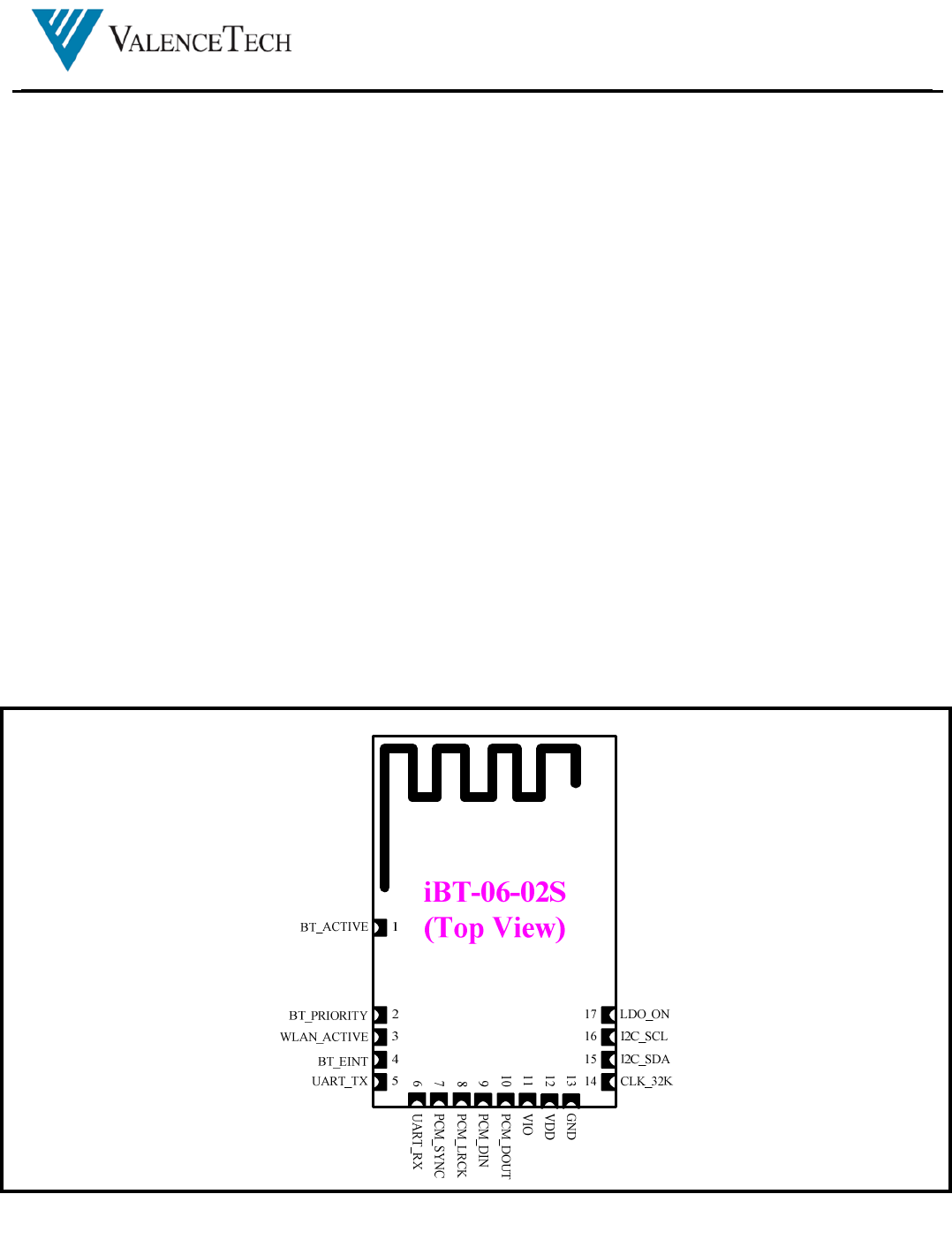
4. Pin Drawing
Figure 1 iBT-06-02S Pin Diagram
iBT-06-02S
Bluetooth Module with HCI Interface
0.5.02 3 / 11 2013-11-21
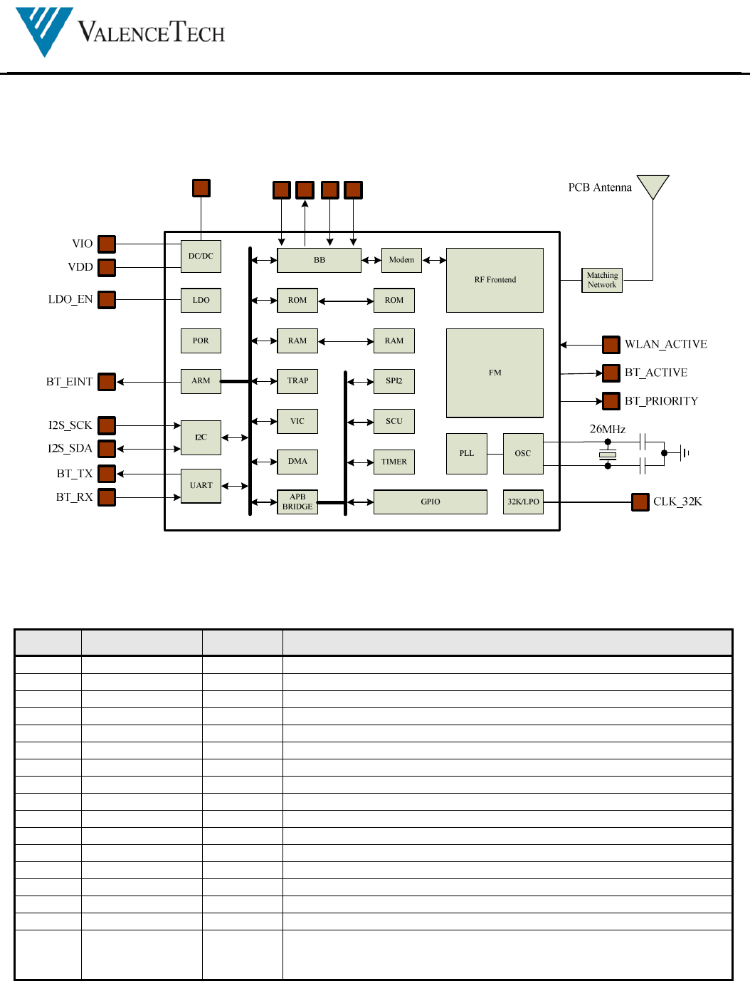
5. Block Diagram
PCM_DIN
PCM_DOUT
PCM_SYNC
PCM_CLK
GND
Figure 2 iBT-06-02S Block Diagram
6. Pin Description
Pin No
Pin Name Pin Type
Pin Descriptions
1 BT_ACTIVE O A “1” indicates that BT is active transmitting data
2 BT_PRIORITY O A “1” indicates that BT request to have priority over WLAN
3 WLAN_ACTIVE
I A “1” indicates that WLAN is active transmitting data
4 BT_EINT O Active high signal to interrupt external MCU
5 BT_TX O Bluetooth UART Data Output
6 BT_RX I Bluetooth UART Data Input
7 PCM_SYNC I PCM data sync
8 PCM_CLK I PCM data clock
9 PCM_DIN I PCM data input
10 PCM_DOUT O PCM data output
11 VIO I/O Supply Voltage
12 VDD Module Supply Voltage
13 GND Module Ground
14 CLK_32K I External 32kHz Clock input
15 I2C_SDA B I2C Data Signal
16 I2C_SCL I I2C Clock Signal
17 LDO_ON I Control signal to enable/disable the internal LDO that provide power to the
internal core. This control signal will also reset the internal core logic.
‘1’ Enable LDO ‘0’ LDO disable
O output pad
I Input IA Analog Input
OA Analog Output
iBT-06-02S
Bluetooth Module with HCI Interface
0.5.02 4 / 11 2013-11-21
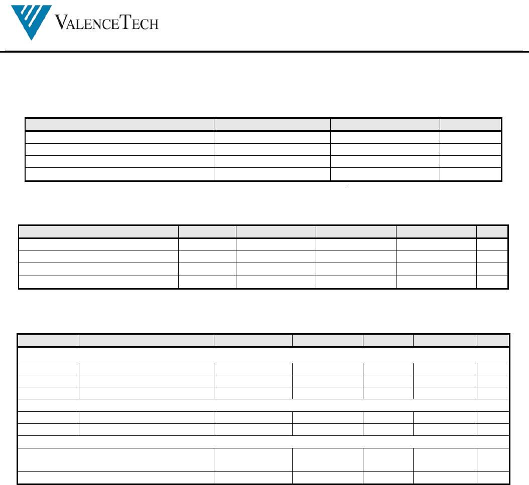
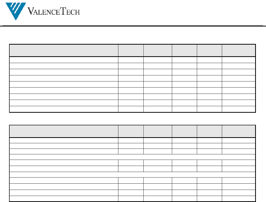
7. Electrical Specification
7.1. Absolute Maximum Rating
Item
Symbol
Rating
Unit
Module Supply Voltage VDD -0.4 to 4.5 V
I/O Supply Voltage VIO -0.4 – 4.0 V
Peak Current Ipk 0 - 70 mA
Storage Temperature T
STG
-20 to 85 °C
7.2. Recommended Operating Condition
Item
Symbol
M
i
in
Typ
Max
Unit
Module Supply Voltage VDD 3.3 4.2 V
I/O Supply Voltage VIO 1.8 3.3 V
RF Operating Temperature 0 25 60 °C
Operating Temperature 0 25 55 °C
7.3. Digital Input / Output Port Characteristics
VDD=3.3V, VIO=3.3V, operating temperature = 25 °C unless specified otherwise
Symbol
Parameter
Condition
Min.
Typ.
Max.
Unit
Input Voltage Levels
V
IL
Input low voltage -0.3
0.25*VIO V
V
IH
Input high voltage 0.7*VIO
VIO+0.3 V
V
sch
Schmitt voltage level 0.3*VIO
0.7*VIO V
Output Voltage Levels
V
OL
Output low voltage I
OL
= -4mA
0.125 V
V
OH
Output high voltage I
OH
= 4mA 0.75*VIO
VIO V
Current Consumption
Operating Current Depends on
profiles 25 mA
Standby Current 0.5 mA
iBT-06-02S
Bluetooth Module with HCI Interface
0.5.02 5 / 11 2013-11-21
7.4. RF Characteristics
VDD=4.0V, operating temperature = 27 °C unless specified otherwise
Receiver Units Miin Typ Max
Bluetooth
Spec
Sensitivity at 0.1% BER dBm -85 ≦ -70
Maximum Receiver Signal at 0.1% BER dBm 0 ≧-20
C/I Co-Channel dB 10 ≦ 11
Adjacent Channel Selectivity C/I +1MHz dB -5 ≦ 0
Adjacent Channel Selectivity C/I -1MHz dB 0 ≦ 0
2
nd
Adjacent Channel Selectivity C/I +2Mhz dB -33 ≦ -30
2
nd
Adjacent Channel Selectivity C/I -2Mhz dB -30 ≦ -20
3
rd
Adjacent Channel Selectivity C/I +3Mhz dB -45 ≦ -40
3
rd
Adjacent Channel Selectivity C/I -3Mhz dB -40 ≦ -40
VDD=4.0V, operating temperature = 27 °C unless specified otherwise
Transmitter Units Miin Typ Max
Bluetooth
Spec
RF Output Power dBm 1.6 -6 to +4
RF Power Control Range dBm -28 2.4 > 16
20dB Bandwidth for modulated Carrier kHz 760 < 1000
Basic Data Rate Adjacent Channel Power
2
nd
Adjacent Channel (+/- 2Mhz) dBm -35 ≦ -20
3
rd
Adjacent Channel (+/- 3Mhz) dBm -40 ≦ -40
Enhance Data Rate Adjacent Channel Power
1
st
Adjacent Channel (+/- 1MHz) dBm -37 ≦ -29
2
nd
Adjacent Channel (+/- 2Mhz) dBm -32 ≦ -20
3
rd
Adjacent Channel (+/- 3Mhz) dBm -40 ≦ -40
Initial Carrier Frequency Tolerance kHz -0.25 4 -75 to +75
iBT-06-02S
Bluetooth Module with HCI Interface
0.5.02 6 / 11 2013-11-21
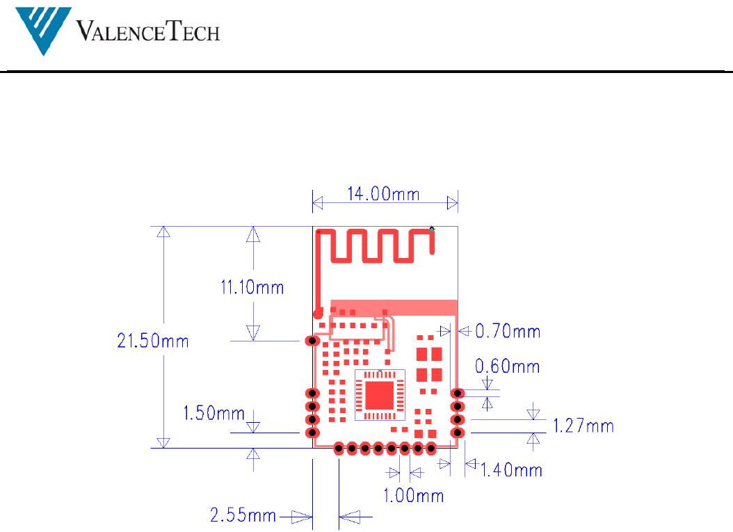
8. Module Dimension
8.1. iBT-06-02S Module Dimension
iBT-06-02S
Bluetooth Module with HCI Interface
0.5.02 7 / 11 2013-11-21
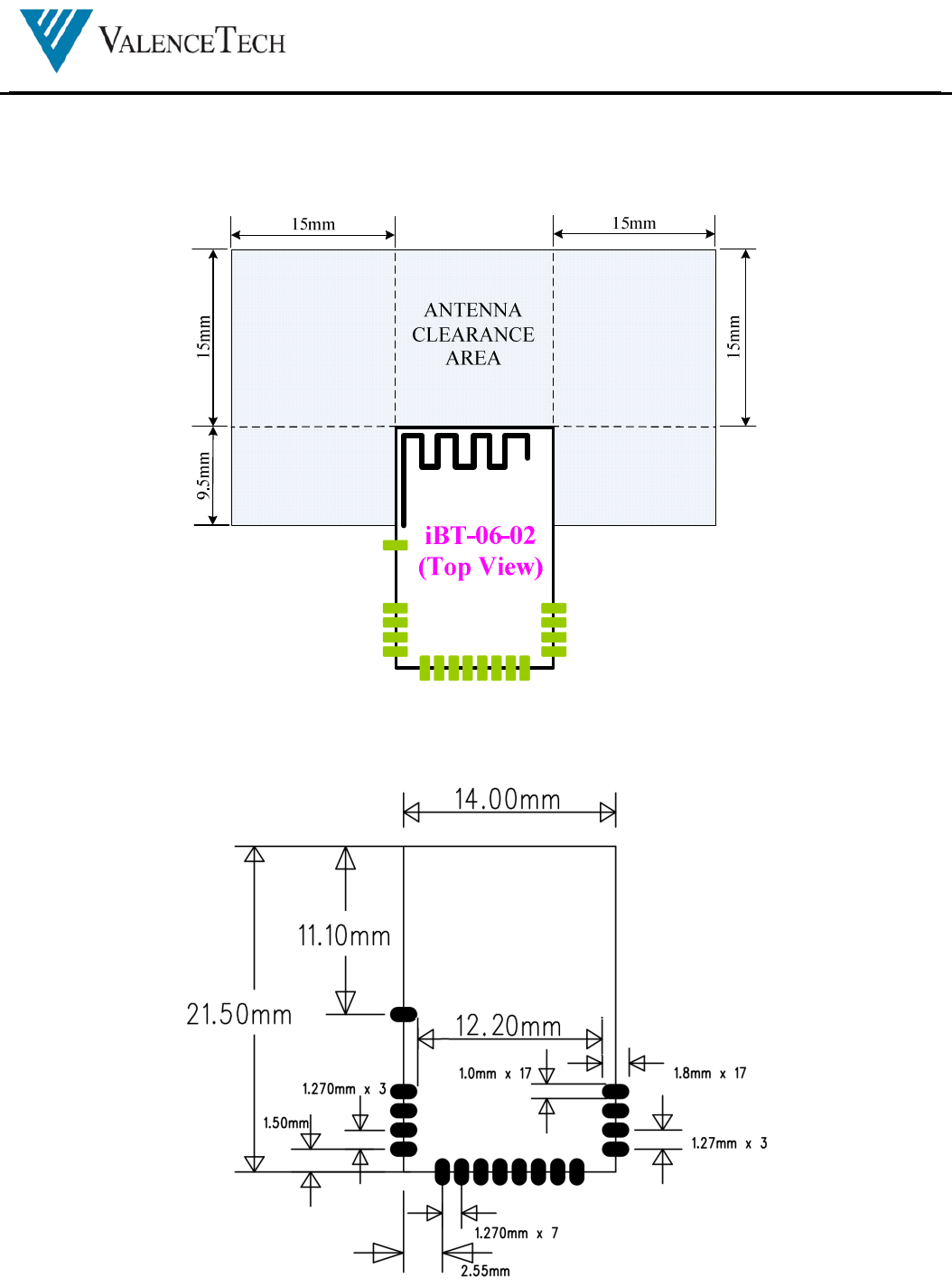
9. PCB Layout Guidelines
9.1. iBT-06-02S Antenna Clearance
9.2. iBT-06-02S PCB Landing Pattern

allows the (OEM) Integator to integrate the RN52 module in
iBT-06-02S
Bluetooth Module with HCI Interface
0.5.02 8 / 11 2013-11-21
10. Regulatory Approval
This section outlines the regulatory information for the iBT-06-02S module for the following countries:
United States
Canada
Japan
10.1. United States
The iBT-06-02S module has received Federal Communications Commission (FCC) CFR47 Telecommunications, Part 15 Subpart
C “Intentional Radiators” modular approval in accordance with Part 15.212 Modular Transmitter approval. Modular approval
to a finished product without obtaining subsequent and separate FCC
approvals for intentional radiation, provided no changes or modifications are made to the module circuitry. Changes or
modifications could void the user’s authority to operate the equipment. The end user must comply with all of the instructions
provided by the Grantee, which indicate installation and/or operating conditions necessary for compliance.
The finished product is required to comply with all applicable FCC equipment authorizations regulations, requirements and
equipment functions not associated with the transmitter module portion. For example, compliance must be demonstrated to
regulations for other transmitter components within the host product; to requirements for unintentional radiators (Part 15 Subpart
B “Unintentional Radiators”), such as digital devices, computer peripherals, radio receivers, etc.; and to additional authorization
requirements for the non-transmitter functions on the transmitter module (i.e., Verification, or Declaration of Conformity) (e.g.,
transmitter modules may also contain digital logic functions) as appropriate.
10.1.1. Labeling and User Information Requirements
The iBT-06-02S module has been labeled with its own FCC ID number, and if the FCC ID is not visible when the module is
installed inside another device, then the outside of the finished product into which the module is installed must also display a label
referring to the enclosed module. This exterior label can use wording as follows:
Contains Transmitter Module FCC ID: ORP-IBT0602S
This device complies with Part15 of the FCC Rules. Operation is subject to the following two conditions: (1) this device may
not cause harmful interference, and (2) this device must accept any interference received, including interference that may cause
undesired operation
A user’s manual for the product should include the following statement:
This equipment has been tested and found to comply with the limits for a Class B digital device, pursuant to part 15 of the FCC
Rules. These limits are designed to provide reasonable protection against harmful interference in a residential installation. This
equipment generates, uses and can radiate radio frequency energy, and if not installed and used in accordance with the
instructions, may cause harmful interference to radio communications. However, there is no guarantee that interference will
not occur in a particular installation. If this equipment does cause harmful interference to radio or television reception, which
can be determined by turning the equipment off and on, the user is encouraged to try to correct the interference by one or more
of the following measures:
Reorient or relocate the receiving antenna.
Increase the separation between the equipment and receiver.
Connect the equipment into an outlet on a circuit different from that to which the receiver is connected.
Consult the dealer or an experienced radio/TV technician for help
Additional information on labeling and user information requirements for Part 15 devices can be found in KDB Publication
784748 available atthe FCC Office of Engineering and Technology (OET) Laboratory Division Knowledge Database (KDB)
http://apps.fcc.gov/oetcf/kdb/index.cfm.
Changes or modifications to this unit not expressly
approved by the party responsible for compliance could void the user’s authority to operate the equipment.

iBT-06-02S
Bluetooth Module with HCI Interface
0.5.02 9 / 11 2013-11-21
10.1.2. RF Exposure
All transmitters regulated by FCC must comply with RF exposure requirements. OET Bulletin 65, Evaluating Compliance with
FCC Guidelines for Human Exposure to Radio Frequency Electromagnetic Fields, provides assistance in determining whether
proposed or existing transmitting facilities, operations or devices comply with limits for human exposure to Radio Frequency (RF)
fields adopted by the Federal Communications Commission (FCC). The bulletin offers guidelines and suggestions for evaluating
compliance.
If appropriate, compliance with exposure guidelines for mobile and unlicensed devices can be accomplished by the use of warning
labels and by providing users with information concerning minimum separation distances from transmitting structures and proper
installation of antennas.
The following statement must be included as a CAUTION statement in manuals and OEM products to alert users of FCC RF
exposure compliance:
The antenna(s) used for this transmitter must not be co-located or operating in conjunction with any other antenna or
transmitter.
If the iBT-06-02S module is used in a portable application (i.e., the antenna is less than20 cm from persons during operation), the
integrator is responsible for performing Specific Absorption Rate (SAR) testing in accordance with FCC rules 2.1091.
10.1.3. Helpful Web Sites
Federal Communications Commission (FCC): http://www.fcc.gov
FCC Office of Engineering and Technology (OET) Laboratory Division Knowledge Database (KDB):
http://apps.fcc.gov/oetcf/kdb/index.cfm
10.2. Canada
The iBT-06-02S module has been certified for use in Canada under Industry Canada (IC) Radio Standards Specification (RSS)
RSS-210 and RSSGen. Modular approval permits the installation of a module in a host device
without the need to recertify the device.
10.2.1. Labeling and User Information Requirements
Labeling Requirements for the Host Device (from Section 3.2.1, RSS-Gen, Issue 3, December 2010): The host device shall be
properly labeled to identify the module within the host device.
The Industry Canada certification label of a module shall be clearly visible at all times when installed in the host device, otherwise
the host device must be labeled to display the Industry Canada certification number of the module, preceded by the words
“Contains transmitter module”, or the word “Contains”, or similar wording expressing the same meaning, as follows:
Contains transmitter module IC: 11691A-IBT0602S
User Manual Notice for License-Exempt Radio Apparatus (from Section 7.1.3 RSS-Gen, Issue 3, December 2010): User manuals
for license-exempt radio apparatus shall contain the following or equivalent notice in a conspicuous location in the user manual or
alternatively on the device or both:
This device complies with Industry Canada license exempt RSS standard(s). Operation is subject to the following two
conditions: (1) this device may not cause interference, and (2) this device must accept any interference, including interference
that may cause undesired operation of the device.
Le présent appareil est conforme aux CNR d'Industrie Canada applicables aux appareils radio exempts de licence.
L'exploitation est autorisée aux deux conditions suivantes: (1) l'appareil ne doit pas produire de brouillage, et (2) l'utilisateur de
l'appareil doit accepter tout brouillage radioélectrique subi, même si le brouillage est susceptible d'en compromettre le
fonctionnement.
EUT has ultra-low output power so that it can be integrated in any host device without
any specific RF exposure limitations

iBT-06-02S
Bluetooth Module with HCI Interface
0.5.02 10 / 11 2013-11-21
Transmitter Antenna (from Section 7.1.2 RSS-Gen,Issue 3, December 2010): User manuals for transmitters shall display the
following notice in a conspicuous location:
Under Industry Canada regulations, this radio transmitter may only operate using an antenna of a type and maximum (or lesser)
gainapproved for the transmitter by Industry Canada. Toreduce potential radio interference to other users,the antenna type and
its gain should be so chosen thatthe equivalent isotropically radiated power (e.i.r.p.) is not more than that necessary for
successful communication.
Conformément à la réglementation d'Industrie Canada, le présent émetteur radio peut fonctionner avec une antenne d'un type et
d'un gain maximal (ou inférieur) approuvé pour l'émetteur par Industrie Canada. Dans le but de réduire les risques de
brouillage radioélectrique à l'intention des autres utilisateurs, il faut choisir le type d'antenne et son gain de sorte que la
puissance isotrope rayonnée équivalente (p.i.r.e.) ne dépasse pas l'intensité nécessaire à l'établissement d'une communication
satisfaisante.
The above notice may be affixed to the device instead of displayed in the user manual.
10.2.1. Helpful Web Sites
Industry Canada: http://www.ic.gc.ca/
iBT-06-02S
Bluetooth Module with HCI Interface
0.5.02 11 / 11 2013-11-21
Valence Semiconductor Design Ltd.
Unit 1, 20/F., APEC Plaza, 49 Hoi Yuen Road, Kwun Tong, Hong Kong
Tel: (852) 2797 3288 Fax: (852) 2776 7770
http://www.valencetech.com
The information in this publication is believed to be accurate in all respects at the time of publication but is subject to change without notice. Valence
Semiconductor Design Ltd. assumes no responsibility for errors and omissions, and disclaims responsibility for any consequences resulting from the use of
information included herein. Additionally, Valence Semiconductor Design Ltd. assumes no responsibility for the functioning of undocumented features or
parameters.