Vancount Wireless Intelligent Control System VC3SMP85 Zigbee Communication Module User Manual
Shanghai Vancount Wireless Intelligent Control System Co.,Ltd. Zigbee Communication Module Users Manual
UserManual.wiki
>
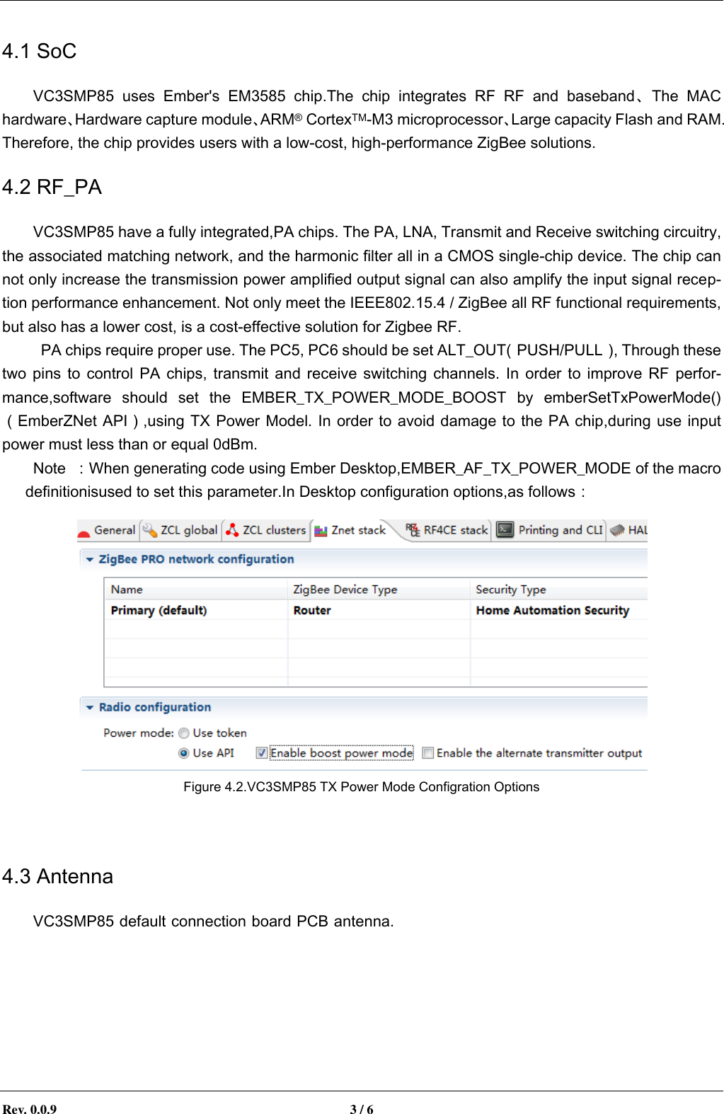
Vancount Wireless Intelligent Control System
>
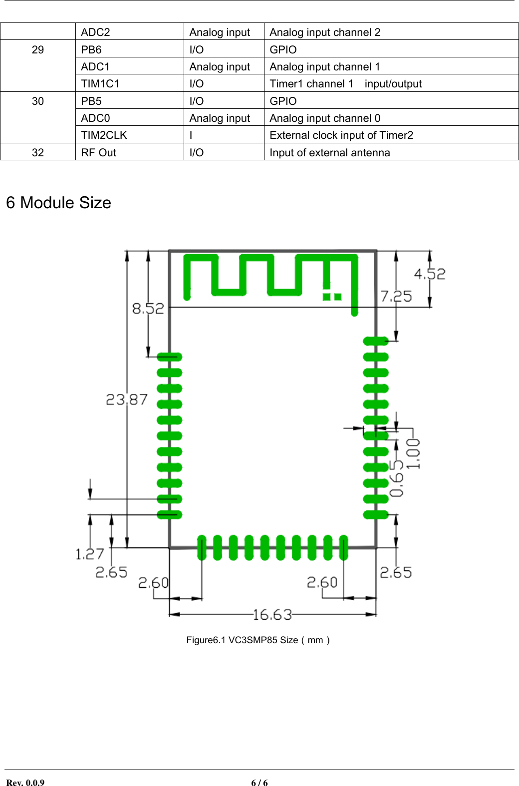
VC3SMP85 User Manual
Users Manual
Navigation menu
Upload a User Manual
Namespaces
Wiki Guide
HTML
PDF
Info
Views
User Manual
Discussion / Help
Navigation