Vancount Wireless Intelligent Control System VC3SMP85 Zigbee Communication Module User Manual
Shanghai Vancount Wireless Intelligent Control System Co.,Ltd. Zigbee Communication Module Users Manual
Users Manual

VC3SMP85
Zigbee module
Instruction Manual
Shanghai Vancount Wireless Intelligent Control System Co.,Ltd

!CAUTION
To prevent damage to the module,be sure to observe the following precautions:
Supply voltage not more than 3.6V
Do not modify the module
Do not wet the module or use the module when your hands are wet
Do not use the module for applications other than communications
Do not force the knock on the module
Welding process ,to prevent electrostatic damage to the module
While using the module,don’t do anything which may cause bodily harm or physical damage
VC3SMP85 模块说明手册
B
e
s
u
r
e
t
o
o
b
s
e
r
v
e
t
h
e
f
o
l
l
o
w
i
n
g
p
r
e
c
a
u
t
i
o
n
s
This device complies with part 15 of the FCC Rules. Operation is subject to the following two
conditions: (1) This device may not cause harmful interference, and (2) this device must accept
any interference received, including interference that may cause undesired operation.
The host label must show “contains FCC ID: 2AINXVC3SMP85”
The device has been evaluated to meet general RF exposure requirement.
To maintain compliance with FCC's RF exposure guidelines, this equipment should be
installed and operated with a minimum distance of 20cm between the radiator and your
body.

· TABLE OF CONTENTS
Rev. 0.0.9 I / I
TABLE OF CONTENTS
1 Description .............................................................................................................................................. 1
2 Features .................................................................................................................................................. 1
3 Electrical Specifications ......................................................................................................................... 1
4 Functional Block Diagram ..................................................................................................................... 2
4.1 SoC ............................................................................................................................................... 3
4.2 RF_PA ........................................................................................................................................... 3
4.3 Antenna ......................................................................................................................................... 3
5 Pin Descriptions ..................................................................................................................................... 4
6 Module Size ............................................................................................................................................ 6
List of Figures
Figure 1.1 VC3SMP85 Module ................................................................................................................. 1
Figure 4.1 VC3SMP85 Functional Block Diagram .................................................................................. 2
Figure 4.2 VC3SMP85 TX Power Mode Configration Options .............................................................. 3
Figure 5.1 VC3SMP85 Pin Descriptions .................................................................................................. 4
Figure 6.1 VC3SMP85 Size ..................................................................................................................... 6
List of Tables
Table 3.1 Absolute Maximum Ratings ..................................................................................................... 1
Table 3.2 Operating Conditions ................................................................................................................ 2
Table 3.3 RF Parameter ........................................................................................................................... 2
Table 3.4 Other Parameter ....................................................................................................................... 2
Table 5.1 Pin Descriptions ....................................................................................................................... 4
Rev. 0.0.9 1 / 6
1 Description
VC3SMP85 have very low power consumption(sleep current1.8µA),High Performance ZigBee
solution.It uses industry-leading ZigBee Pro Stack——EmberZNet,provides stable and reliable ZigBee
network.VC3SMP85 moudle integrated ARM®Cortex-M3 32-bit microprocesso,have extensive memory
resources and I / O interfaces,Customers can quickly achieve simple or complex product development.
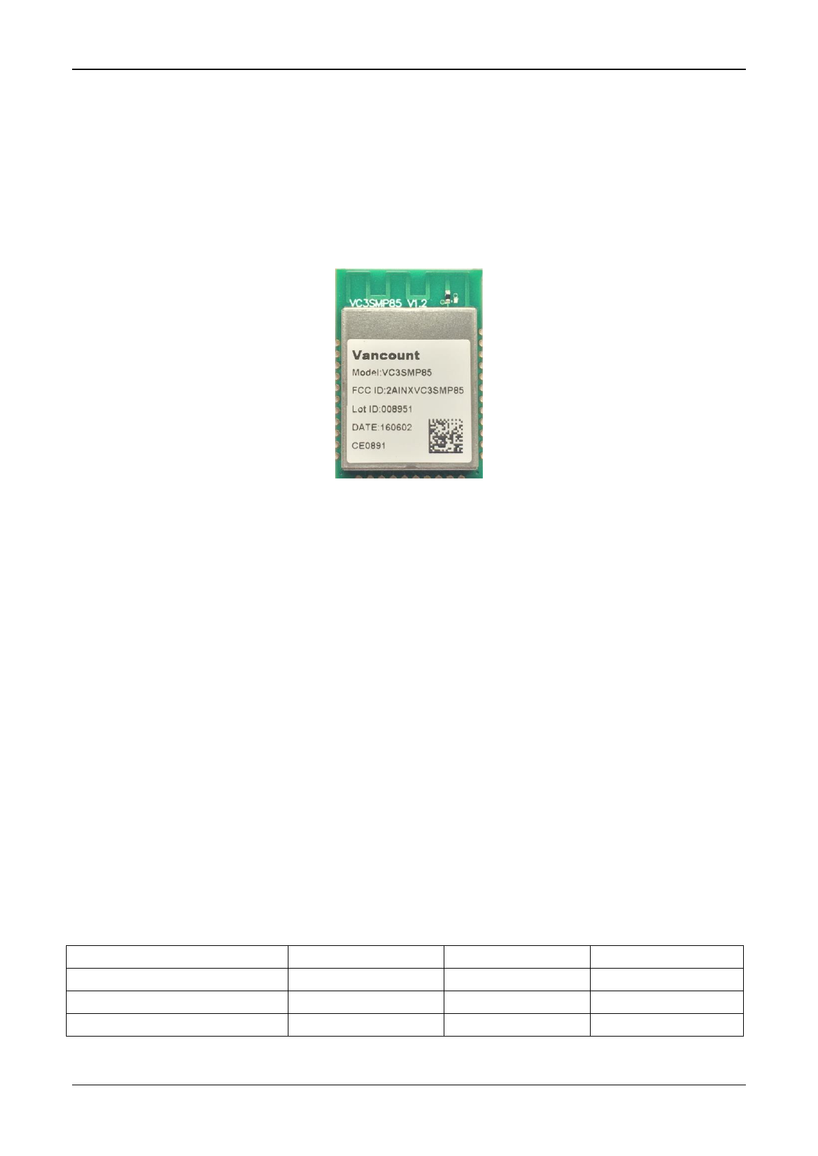
Figure 1.1.VC3SMP85 Module
2 Features
32-bit ARM® Cortex-M3 processor
Operation at:6, 12 or 24MHz
+20dB normal mode output power
512KB flash,64KB RAM Memory
Low deep sleep current ,with retained RAM and GPIO: 1.8µA.Sleep modes seletables
Single voltage operation:2.1-3.6V with internal 1.8 and 1.25V regulators
Optional OTA firmware upgrade mode
AES-128 encryption accelerator
Flexible ADC,UART/SPI/TWI serial communications
Temperature range: -40 to +85℃
Normal mode link budget up to 116dB;configurable up to 120dB
3 Electrical Specifications
Table 3.1.Absolute Maximum Ratings
Parameter
Min
Max
Unit
Regulator input voltage(VDD)
-0.3
+3.6
V
Voltage on any GPIO
-0.3
VDD+0.3
V
Analog,Memory and Core volt-
-0.3
+2.0
V
Rev. 0.0.9 2 / 6
age
RF Input Power
——
+5
dBm
Storage temperature
-40
+125
℃
Table 3.2.Operating Conditions
Parameter
Min
Typ
Max
Uint
Supply voltage(VDD)
2.1
3.3
+3.6
V
Operating temperature range
-40
25
+85
℃
Table 3.3.RF Parameter
Parameter
Min
Typ
Max
Unit
Frequency range
2405
——
2480
MHz
Sensitivity(1%PER,Boost Mode)
-102
——
-94
dBm
TX Power
——
+20
+21
dBm
Frequency tolerance(@25℃)
-96.2
——
+96.2
kHz
Note :In the open distance test,the transmission distance up to 0.497 mile
Table 3.4.Other Parameter
Parameter
Min
Typ
Min
Unit
Total TX current(+20dBm,Boost
Mode)
——
157.5
——
mA
Total RX current(Boost Mode)
——
37.5
——
mA
Sleep Current
——
1.6
——
µA
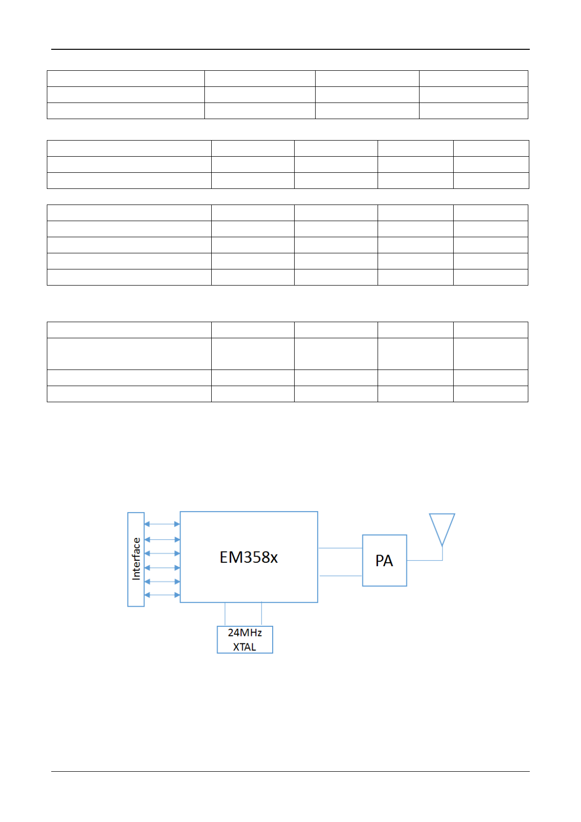
4 Functional Block Diagram
VC3SMP85 with high performance ZigBee SoC and PA
Figure4.1 shows functional block diagram of the VC3SMP85 Module
Figure 4.1.VC3SMP85 Module functional block diagram
Rev. 0.0.9 3 / 6
4.1 SoC
VC3SMP85 uses Ember's EM3585 chip.The chip integrates RF RF and baseband、The MAC
hardware、Hardware capture module、ARM® CortexTM-M3 microprocessor、Large capacity Flash and RAM.
Therefore, the chip provides users with a low-cost, high-performance ZigBee solutions.
4.2 RF_PA
VC3SMP85 have a fully integrated,PA chips. The PA, LNA, Transmit and Receive switching circuitry,
the associated matching network, and the harmonic filter all in a CMOS single-chip device. The chip can
not only increase the transmission power amplified output signal can also amplify the input signal recep-
tion performance enhancement. Not only meet the IEEE802.15.4 / ZigBee all RF functional requirements,
but also has a lower cost, is a cost-effective solution for Zigbee RF.
PA chips require proper use. The PC5, PC6 should be set ALT_OUT(PUSH/PULL), Through these
two pins to control PA chips, transmit and receive switching channels. In order to improve RF perfor-
mance,software should set the EMBER_TX_POWER_MODE_BOOST by emberSetTxPowerMode()
(EmberZNet API),using TX Power Model. In order to avoid damage to the PA chip,during use input
power must less than or equal 0dBm.
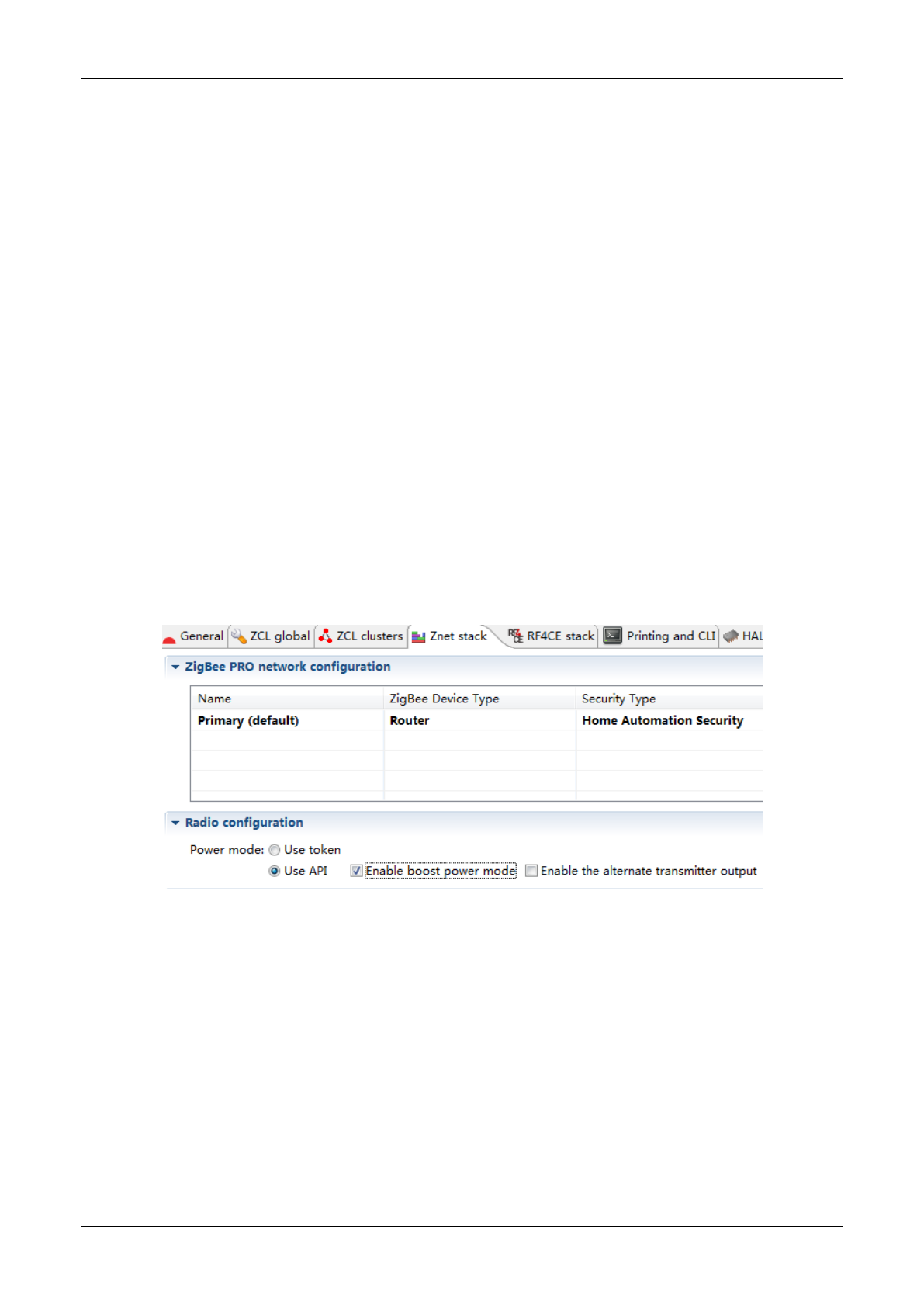
Note :When generating code using Ember Desktop,EMBER_AF_TX_POWER_MODE of the macro
definitionisused to set this parameter.In Desktop configuration options,as follows:
Figure 4.2.VC3SMP85 TX Power Mode Configration Options
4.3 Antenna
VC3SMP85 default connection board PCB antenna.
In order to guarantee the transmission performance, it can not exist around the module ground
plane.When using an extenna antenna,you need to pay attention to the antenna lead-out portion of the
motherboard design..Ensure the transmission line impedance matching. Avoid the impedance mismatch
caused by radio signal reflection, the actual antenna signal power drops, affect the transmission distance.
Rev. 0.0.9 4 / 6
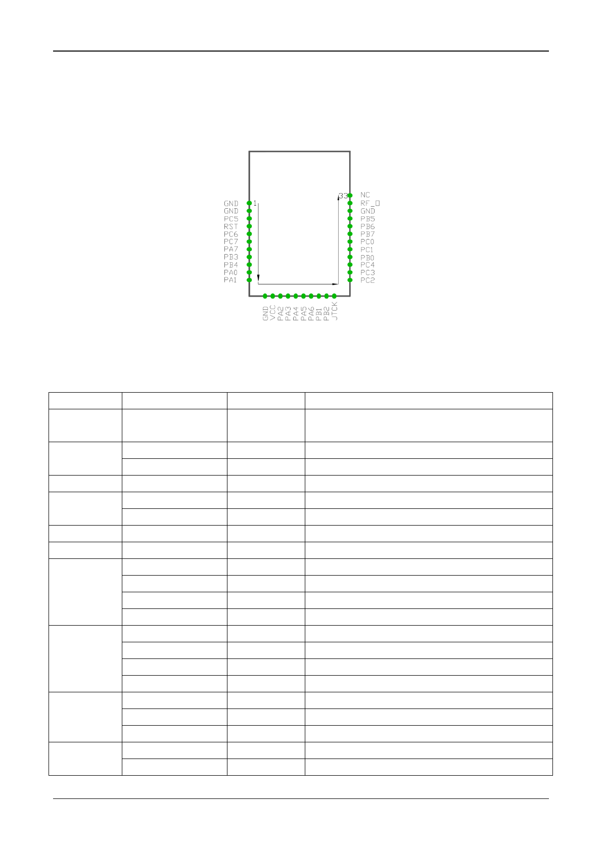
5 Pin Description
Figure 5.1.VC3SMP85 pin descriptions
Table 5.1.pin descriptions
Pin#
Signal
Direction
Description
1、2、12、31、
33
GND
——
——
3
PC5
I/O
GPIO
TX_ACTIVE
O
Output high level in TX mode
4
RESET
I
Low voltage reset
5
PC6
I/O
GPIO
nTX_ACTIVE
O
Output low level in TX mode
6
PC7
I/O
GPIO
7
PA7
I/O
GPIO
8
PB3
I/O
GPIO
SC1nCTS
I
CTS of UART
SC1SCLK
I/O
Clock line of SPI
TIM2C3
I/O
Timer 2 channel 3 input/output
9
PB4
I/O
GPIO
TIM2C4
I/O
Timer 2channel 4 input/output
SC1nRTS
O
RTS of UART
SC1nSSEL
I
SPI Slave Select
10
PA0
I/O
GPIO
TIM2C1
I/O
Timer2 channel 1 input/output
SC2MOSI
I/O
SPI host output、slave input
11
PA1
I/O
GPIO
TIM2C3
I/O
Timer 2 cahnne 3 input/output

Rev. 0.0.9 5 / 6
SC2MISO
I/O
SPI host input、slave output
13
VDD
——
Power supply(2.1——3.6V)
14
PA2
I/O
GPIO
TIM2C4
I/O
Timer 2 channel 4 input/output
SC2SCLK
I/O
Clock line of SPI
SC2SCL
I/O
Clock line of cerial controller
15
PA3
I/O
GPIO
SC2SSEL
I
SPI Slave Select
TIM2C2
I/O
Timer2 channel 2 input/output
16
PA4
I/O
GPIO
ADC4
Analog input
Analog input channel 4
17
PA5
I/O
GPIO
ADC5
Analog input
Analog input channel 5
nBootMode
I
When the chip enable, start Bootloade control pin
18
PA6
I/O
GPIO
TIM1C3
I/O
Timer 1 channel 3 input/output
19
PB1
I/O
GPIO
SC1MISO
O
SPI slave output
SC1MOSI
O
SPI host output
SC1SDA
I/O
Date cable of serial communications
SC1TXD
O
TX interface of UART
TIM2C1
I/O
Timer2 channel 1 input/output
20
PB2
I/O
GPIO
SC1MISO
I
SPI host input
SC1MOSI
I
SPI slave input
SC1SCL
I/O
Clock line of serial communications
SC1RXD
I
Rx interface of UART
TIM2C2
I/O
Timer2 channel 2 input/output
21
SWCLK
I/O
Clock line of SWD interface
JTCK
I
Clock line of JTAG interface
22
PC2
I/O
GPIO
23
PC3
I/O
GPIO
24
PC4
I/O
GPIO
SWDIO
I/O
Date cable of SWD interface
25
PB0
I/O
GPIO
IRQA
I
External interrupt sources A
VREF
I/O
Input/output of ADC reference level
TIM1CLK
I
External clock input of Timer 1
26
PC1
I/O
GPIO
ADC3
I
Analog input channel 3
27
PC0
I/O
GPIO
28
PB7
I/O
GPIO
Rev. 0.0.9 6 / 6
ADC2
Analog input
Analog input channel 2
29
PB6
I/O
GPIO
ADC1
Analog input
Analog input channel 1
TIM1C1
I/O
Timer1 channel 1 input/output
30
PB5
I/O
GPIO
ADC0
Analog input
Analog input channel 0
TIM2CLK
I
External clock input of Timer2
32
RF Out
I/O
Input of external antenna
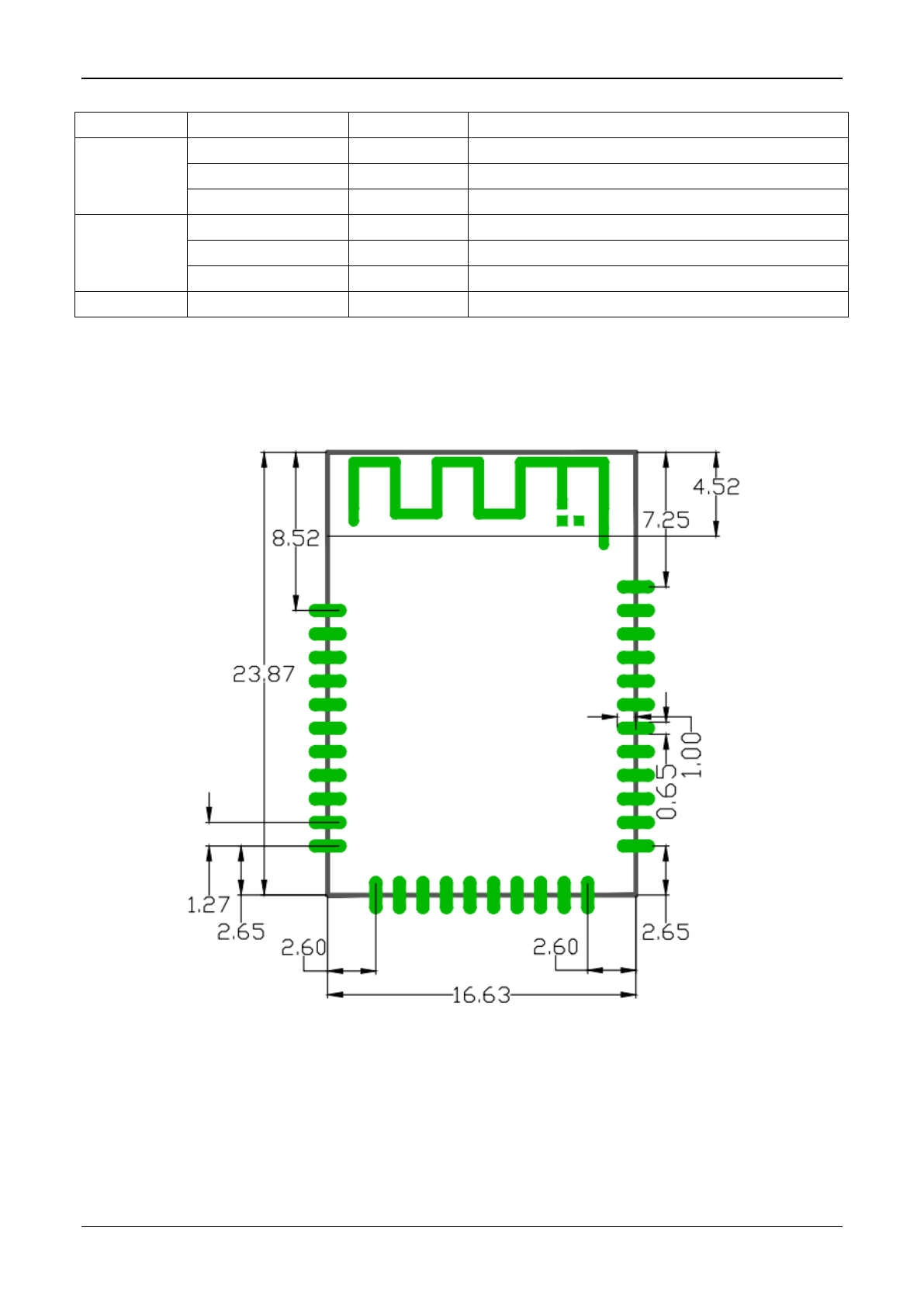
6 Module Size
Figure6.1 VC3SMP85 Size(mm)