Vision Technics VWM-1G01A Modular Wireless Card User Manual VWM 1G01A Manual ENG 050530 1
Vision Technics Co., Ltd. Modular Wireless Card VWM 1G01A Manual ENG 050530 1
Users Manual

A
Au
ud
di
io
o
D
Da
at
ta
a
T
Tr
ra
an
ns
sc
ce
ei
iv
ve
er
r
R
RF
F
M
Mo
od
du
ul
le
e’
’s
s
M
Ma
an
nu
ua
al
l
VISION TECHNICS VWM-1G01A
VISION TECHNICS ©Copyrights 2005. All rights reserved
1
VWM-1G01A

A
Au
ud
di
io
o
D
Da
at
ta
a
T
Tr
ra
an
ns
sc
ce
ei
iv
ve
er
r
R
RF
F
M
Mo
od
du
ul
le
e’
’s
s
M
Ma
an
nu
ua
al
l
VISION TECHNICS VWM-1G01A
VISION TECHNICS ©Copyrights 2005. All rights reserved
2
1. Product Introduction
The Wireless LAN is a transceiver, which installed in the speaker system receiving and
transmitting the Audio sound, can catch the Amp sound through the wireless.
This product composed of the total 40 pins, can transmit and receive the data in the air
through one unit module with an antenna.
The antenna has the 2dBi(peak) gain. And also, the installed oscillator frequency is
operated as 44MHz and 3.3V and is able to get the data maximizing 11Mbps.
The channel use the 1~13CH and also automatically scan the best optimized channel
without noise.

A
Au
ud
di
io
o
D
Da
at
ta
a
T
Tr
ra
an
ns
sc
ce
ei
iv
ve
er
r
R
RF
F
M
Mo
od
du
ul
le
e’
’s
s
M
Ma
an
nu
ua
al
l
VISION TECHNICS VWM-1G01A
VISION TECHNICS ©Copyrights 2005. All rights reserved
3
2. Using Method.
This module is the developed digital transmission system to catch the audio sound through the
wireless method from the transmitting and the receiving device, which transfer the inputted analog
signal from the Amp to the digital signal.
Link +3.3V to the 37/39 pin# of the module and the GND to the 36/38/40 pin#, thus, supply the
power.
When inputting the initial power, this Channel will be shifted to the best optimized condition to
receive and transmit the high qualified sound between the transmitting module and receiving
module.
This module can add the amp part and the other sound circuits in the receiving speaker system.
Remark※
Please refer the pin description of the module, the block diagram, the interface and the

A
Au
ud
di
io
o
D
Da
at
ta
a
T
Tr
ra
an
ns
sc
ce
ei
iv
ve
er
r
R
RF
F
M
Mo
od
du
ul
le
e’
’s
s
M
Ma
an
nu
ua
al
l
VISION TECHNICS VWM-1G01A
VISION TECHNICS ©Copyrights 2005. All rights reserved
4
mechanical dimension.
Attachment 1. Pin Configuration
* N.C : NO CONNECTION
* GPIO : GENERAL PURPOSE IN/OUT PORT
DGND
NO
1
2
3
4
5
6
7
8
9
10
11
12
13
14
15
16
17
18
19
20
21
22
23
24
25
26
27
31
PIN NAME
EEPROM_ENB
EXT_UXTALIN
DGND
N.C
GPA8
USBDPLUS
USBDMINUS
SDA
SCL
DGND
GPB11
GPB10
GPB9
GPB7
GPB5
GPB2
GPA3
GPA2
GPA1
GPA0
TDO
JTAG_RST
TDI
RESET
AGND
VCC33
VCC33
DESCRIPTION
28
29
30
32
33
34
35
36
37
38
39
40
GPB8
GPB6
GPB4
GPB3
GPB1
GPB0
GPA7
GPA6
TCK
TMS
AGND
AGND
EEPROM enable control input
USB clock crystal input (48MHz)
Digital Ground
NO CONNECTION
USB D+
USB D-
Serial Data
Serial Clock Input
Digital Ground
MCLK
SDATA
LRCLK
SCLK
JTAG serial output data
JTAG reset signal, Active low
JTAG serial input data, Active low
Reset signal for internal registers, Active low
Analog Ground
Supply for digital peripheral blocks (3.3V)
Supply for digital peripheral blocks (3.3V)
Host interface address/data multiplexed GPIO
Digital Ground
SPDIF OUT
SPDIF IN
JTAG clock signal, Active low
JTAG test mode signal, Active low
Analog Ground
Analog Ground
Host interface address/data multiplexed GPIO
Host interface address/data multiplexed GPIO
Host interface address/data multiplexed GPIO
Host interface address/data multiplexed GPIO
Host interface address/data multiplexed GPIO
Host interface address/data multiplexed GPIO
Host interface address/data multiplexed GPIO
Host interface address/data multiplexed GPIO
Host interface address/data multiplexed GPIO
Host interface address/data multiplexed GPIO
Host interface address/data multiplexed GPIO
GPIO
A
Au
ud
di
io
o
D
Da
at
ta
a
T
Tr
ra
an
ns
sc
ce
ei
iv
ve
er
r
R
RF
F
M
Mo
od
du
ul
le
e’
’s
s
M
Ma
an
nu
ua
al
l
VISION TECHNICS VWM-1G01A
VISION TECHNICS ©Copyrights 2005. All rights reserved
5
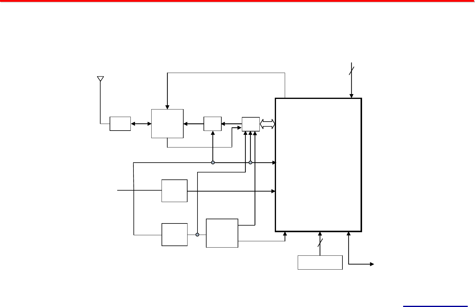
Attachment 2. Block Diagram
GDM5103
WLAN B.B
PA
T/R
Switch
BPF
Antenna
EEPROM
RF
LDO
1.8V
LDO
2.8V
OSC
44MHz
>
+3.3V
●
RF-COM RF-OUT
RF-OUT
RF-IN
Switch Signal
CLK-REF
7
Down load (JTAG)
GPIO &
Serial interface
(256k)
GRF5101
2
GDM5103
WLAN B.B
PA
T/R
Switch
BPF
Antenna
EEPROM
RF
LDO
1.8V
LDO
2.8V
OSC
44MHz
>
+3.3V
●
RF-COM RF-OUT
RF-OUT
RF-IN
Switch Signal
CLK-REF
7
Down load (JTAG)
GPIO &
Serial interface
(256k)
GRF5101
2
A
Au
ud
di
io
o
D
Da
at
ta
a
T
Tr
ra
an
ns
sc
ce
ei
iv
ve
er
r
R
RF
F
M
Mo
od
du
ul
le
e’
’s
s
M
Ma
an
nu
ua
al
l
VISION TECHNICS VWM-1G01A
VISION TECHNICS ©Copyrights 2005. All rights reserved
6
Attachment 3-1. External Audio ADC/DAC Interface
Audio ADC/DAC interface provides a high quality multi resolution(16/18/20/24-bit) digital audio connection to external audio devices. ADI interface
supports I2S audio format as well as optional left-justified or right-justified audio format.
ADI interface produces one 64-bit frame at the audio sample frequency using a bit clock and frame sync signal. ADI interface supports 32KHz,
44.1KHz or 48KHz audio sampling frequency, of which 256 or 384 times main clock can be generated from on-chip audio clock oscillator or external
clock signal by interface mode programming.
Pin Name I/O Type Description
AUD_MCLK programmable clock audio oversampled clock
This clock can be programmed 256 or 384 times
AUDLRCLK
AUD_SCLK programmable clock audio serial data bit clock
This clock is fixed at 64 times AUDLRCLK
AUD_LRCLK programmable clock audio frame synchronization clock
This clock can be programmed 32KHz, 44.1KHz or
48KHz
AUD_DATA programmable serial data audio serial data used for sending playback data to DAC
and receiving data from ADC
16-bit data format with I2C, left-justified or right-justified
interface
MS 14 13 2 1 LS MS 14 13 2 1 LS
Left Right
•I
2S interface
AUDLRCLK
AUDOUT
AUDSCLK
32 AUDBCLK
MS 14 13 2 1 LS MS 14 13 2 1 LS
Left Right
• Left-justified interface
AUDLRCLK
AUDOUT
AUDSCLK
MS 14 13 2 1 LS MS 14 13 2 1 LS
Left Right
• Right-justified interface
AUDLRCLK
AUDOUT
AUSCLK
MS MS

A
Au
ud
di
io
o
D
Da
at
ta
a
T
Tr
ra
an
ns
sc
ce
ei
iv
ve
er
r
R
RF
F
M
Mo
od
du
ul
le
e’
’s
s
M
Ma
an
nu
ua
al
l
VISION TECHNICS VWM-1G01A
VISION TECHNICS ©Copyrights 2005. All rights reserved
7
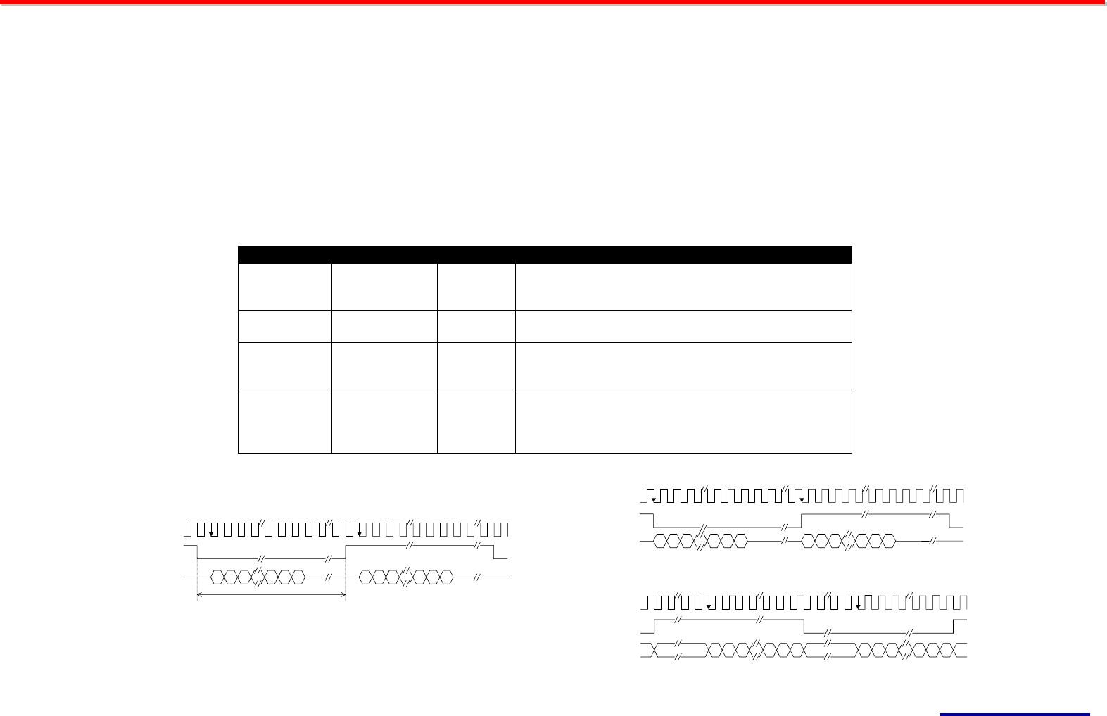
Attachment 3-2. JTAG Interface
This module supports IEEE1149.1 standard specification compliant interface. This interface supports basic test commands such as EXTEST,
SMAPLE, BYPASS, and IDCODE. Beside of this, JTAG interface can be used as communication channel with GCT enhanced on-chip hardware
debugger controller of GDM5103 within the module. Using on-chip debugger controller, off-chip debug handler or external host can access internal
peripheral device registers, internal memory and executes real-timing hardware debugging and monitoring of on-chip embedded RISC processor.
Also, external host can communicate on-chip RISC processor through JTAG with on-chip hardware managed channel buffer. There are sixteen
debug registers specified and these will be used in GCT own development chip manager software. The length of instruction register in JTAG
interface is 6bit and that of debug data register is 32bit. Table shows the summary of TAP instructions supported in GDM5103.
Instruction Opcode Description
EXTEST 0x000000 EXTEST initiates testing of external circuitry, typically board-level
interconnects and off chip circuitry. EXTEST connects the Boundary-
Scan register between TDI and TDO in the SHIFT_DR state only. When
EXTEXT is selected, all output signal pin values are driven by values
shifted into the Boundary-Scan register and may change only on the
falling-edge of TCK in the Update_DR state. Also, when EXTEST is
selected, all system input pin states must be loaded into the Boundary-
Scan register on the rising-edge of TCK in the Capture_DR state. Values
shifted into input latches in the Boundary-Scan register are never used
by the processor’s internal logic.
SAMPLE 0x000001
SAMPLE / PRELOAD performs two functions:
• When the TAP controller is in the Capture-DR state, the SAMPLE
instruction occurs on the rising edge of TCK and provides a snapshot of
the component’s normal operation without interfering with that normal
operation. The instruction causes Boundary-Scan register cells
associated with outputs to SAMPLE the value being driven by or to the
processor.
• When the TAP controller is in the Update-DR state, the PRELOAD
instruction occurs on the falling edge of TCK. This instruction causes the
transfer of data held in the Boundary-Scan cells to the slave register
cells. Typically the slave latched data is then applied to the system
outputs by means of the EXTEST instruction.
IDCODE 0x011111
IDCODE is used in conjunction with the device identification register. It
connects the identification register between TDI and TDO in the Shift_DR
state. When selected, IDCODE parallel-loads the hard-wired
identification code (32 bits) on TDO into the identification register on the
rising edge of TCK in the Capture_DR state.
NOTE: The device identification register is not altered by data being
shifted in on TDI.
DEBUG
(Private Instruction)
0x10SSSS DEBUG instruction select the DEBUGReg with address indicator SSSS.
• When the TAP controller is in the Capture-DR state, the DEBUG
instruction occurs on the rising edge of TCK and executes a snapshot of
DEBUG register addressed SSSS into DEBUGReg.
• When the TAP controller is in the Update-DR state, the DEBUG
instruction occurs on the falling edge of TCK. This instruction causes the
transfer of data held in DEBUGReg to DEBUG register addressed SSSS.
BYPASS 0x111111 BYPASS instruction selects the Bypass register between TDI and TDO
pins while in SHIFT_DR state, effectively bypassing the processor’s test
logic. 0 is captured in the CAPTURE_DR state. While this instruction is in
effect, all other test data registers have no effect on the operation of the
system. Test data registers with both test and system functionality
perform their system functions when this instruction is selected
A
Au
ud
di
io
o
D
Da
at
ta
a
T
Tr
ra
an
ns
sc
ce
ei
iv
ve
er
r
R
RF
F
M
Mo
od
du
ul
le
e’
’s
s
M
Ma
an
nu
ua
al
l
VISION TECHNICS VWM-1G01A
VISION TECHNICS ©Copyrights 2005. All rights reserved
8
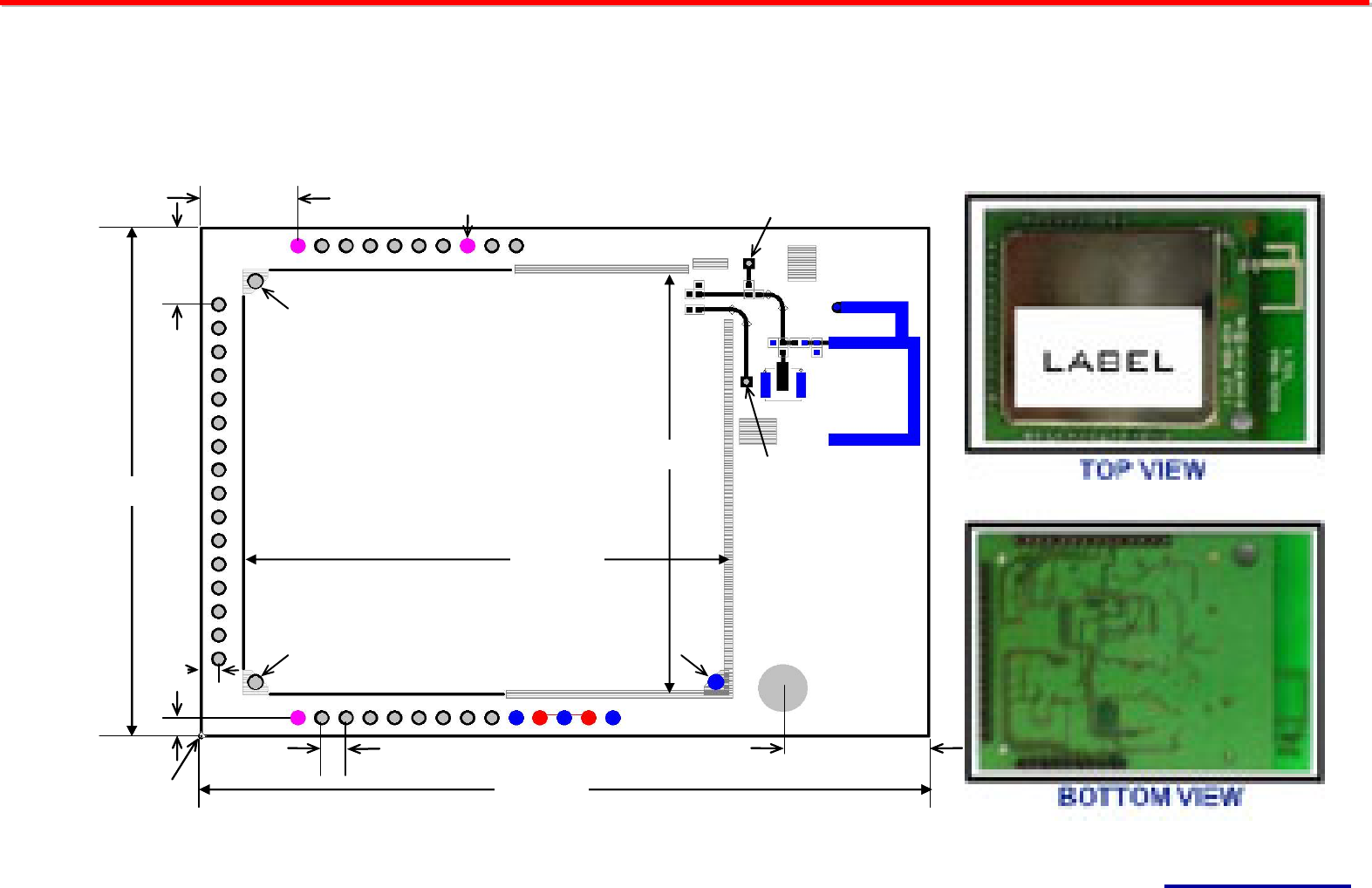
Attachment 4. Mechanical Dimension
43.0 mm
60.0 mm
12.0 mm
01
10
11
26
27 40
41(ANT2)
(X,Y:45,30)
42(ANT1)
(X,Y:45.2,40)
Hole ¢= 4.0 mm
6.5 mm
8.0 mm
36.0 mm
40.0 mm
Reference Position
(X,Y:0,0)
2.0 mm
Hole Center Position
(X,Y:4.5,4.5)
Hole ¢= 0.8 mm
Land ¢= 1.3 mm
1.5 mm
1.5 mm
Hole ¢= 0.4 mm
Land ¢= 1.0 mm
Hole Center Position
(X,Y:4.5,38.5)
Hole Center Position
(X,Y:42.5,4.5)
* Shielding-Can Information
- Size 40.2 * 36.2 mm
- Fixing holes : 3 Points
( Hole ¢= 0.55 mm)
- Avoidance of direct contact with
top Pattern from Pin11 to Pin26

A
Au
ud
di
io
o
D
Da
at
ta
a
T
Tr
ra
an
ns
sc
ce
ei
iv
ve
er
r
R
RF
F
M
Mo
od
du
ul
le
e’
’s
s
M
Ma
an
nu
ua
al
l
VISION TECHNICS VWM-1G01A
VISION TECHNICS ©Copyrights 2005. All rights reserved
9
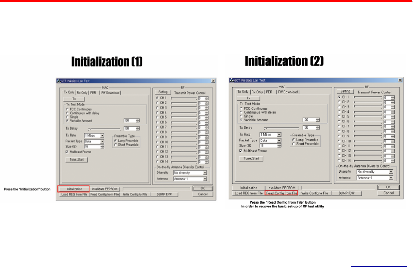
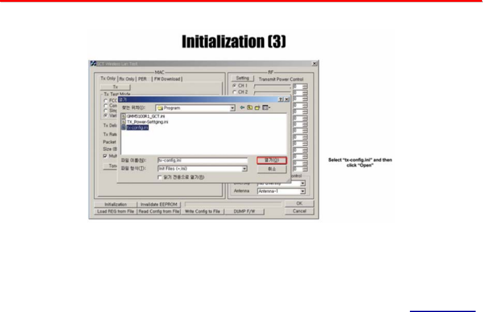
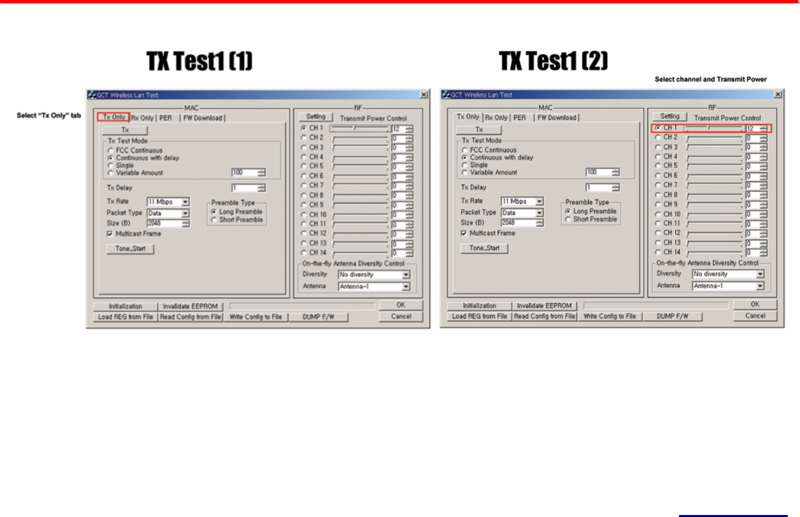
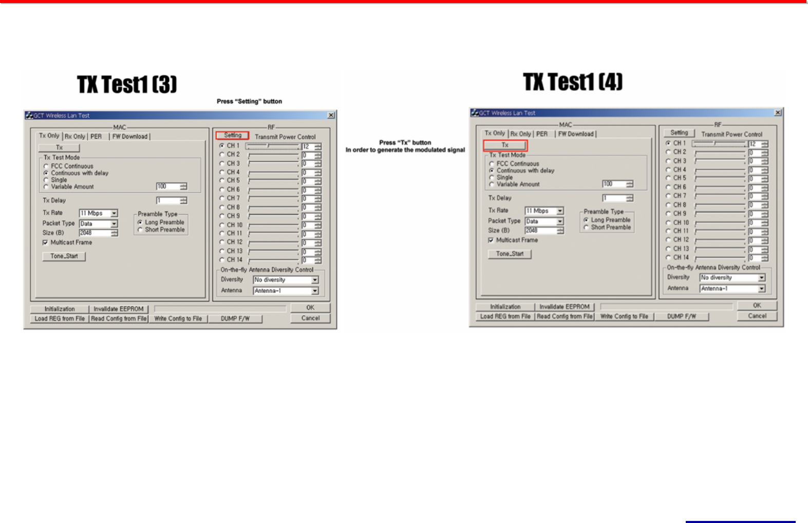
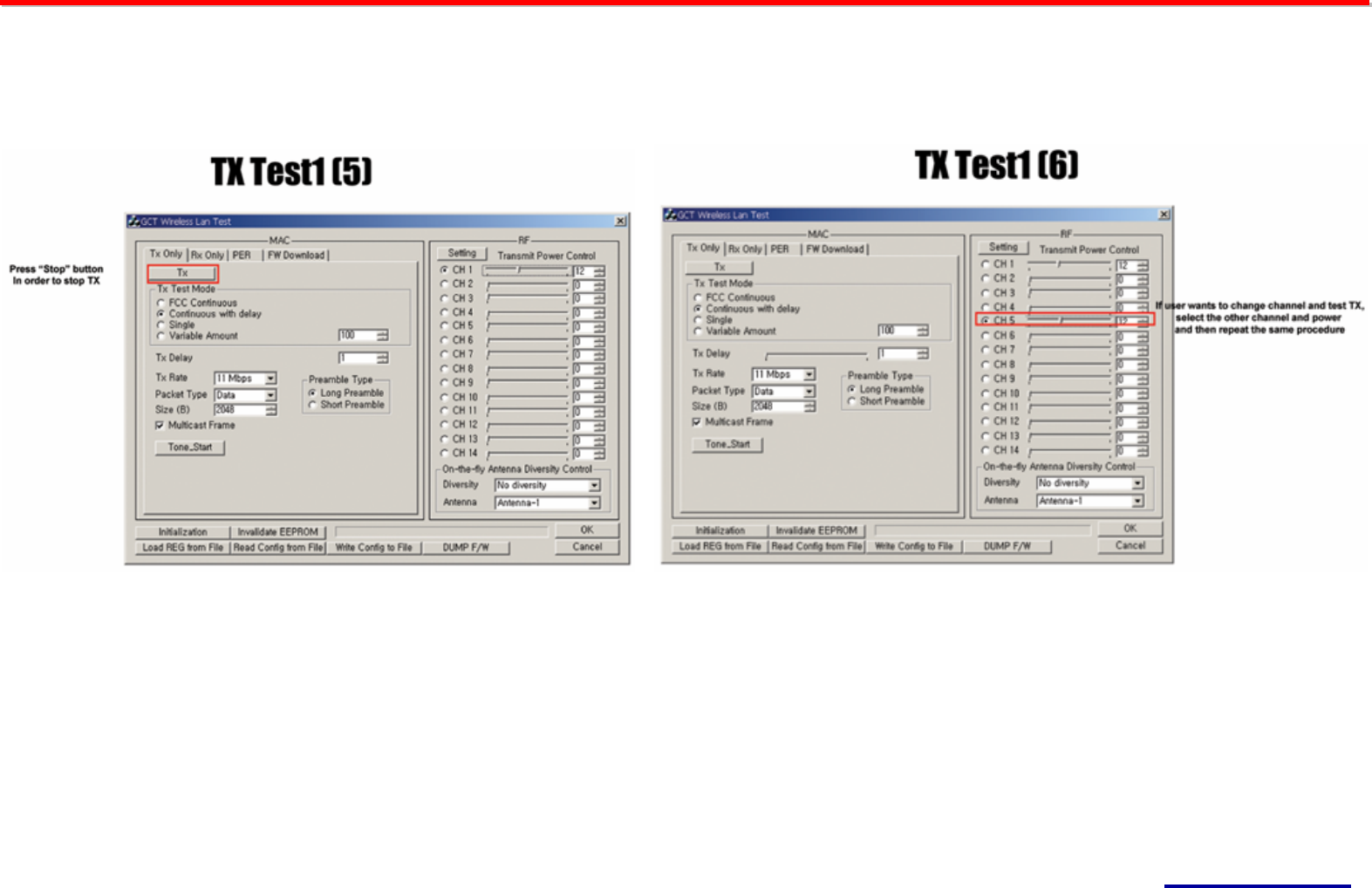
3. Install method
■ Environment Set-up
■ Initialization
■ TX Test1: Modulated signal generation
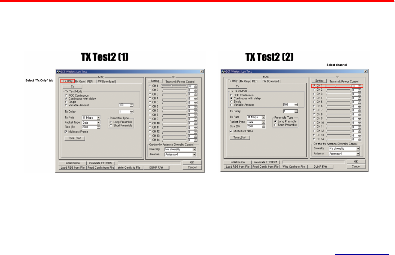
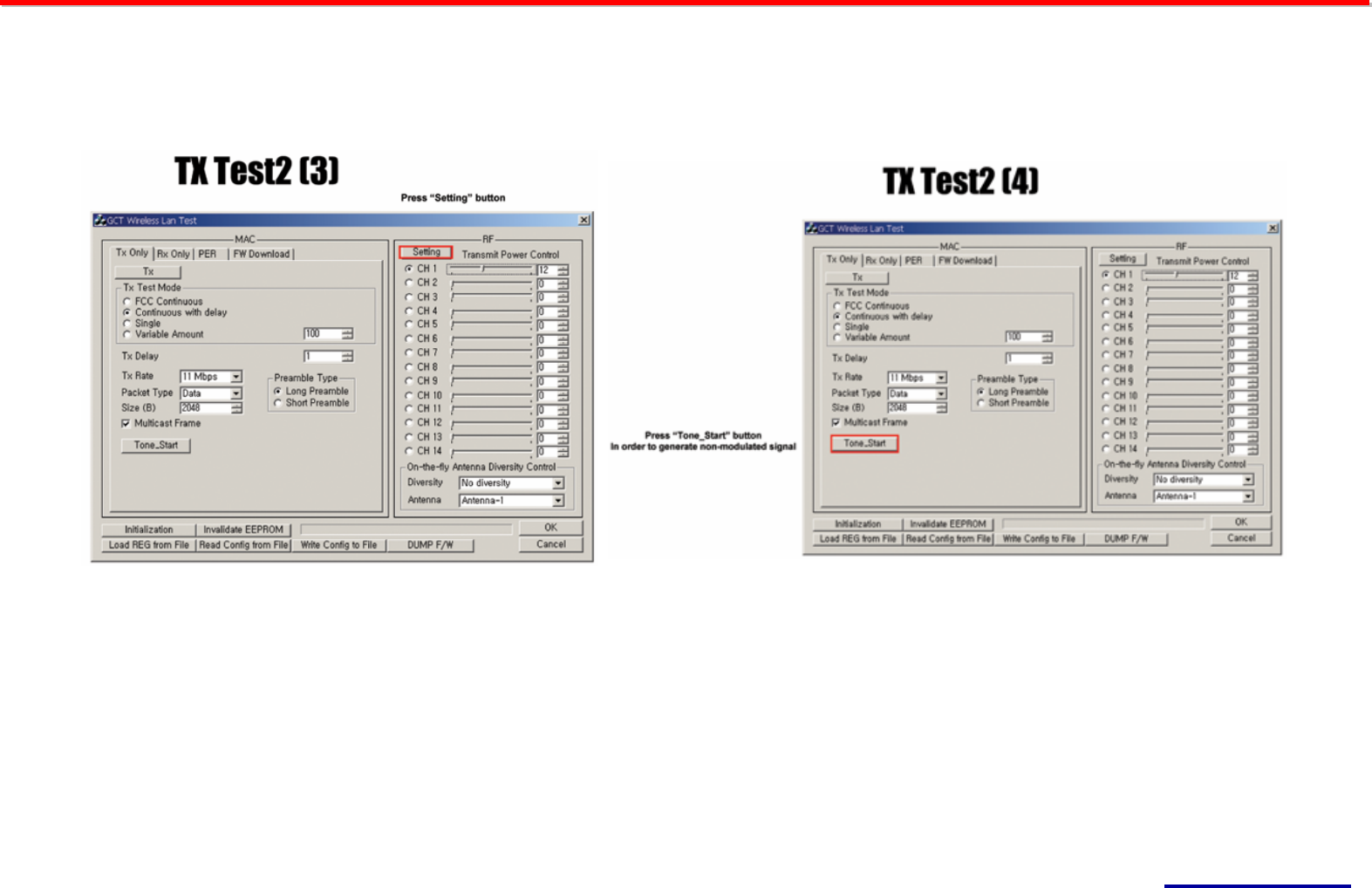
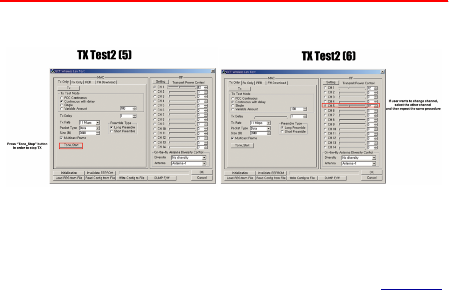
■ TX Test2: Non-modulated signal generation
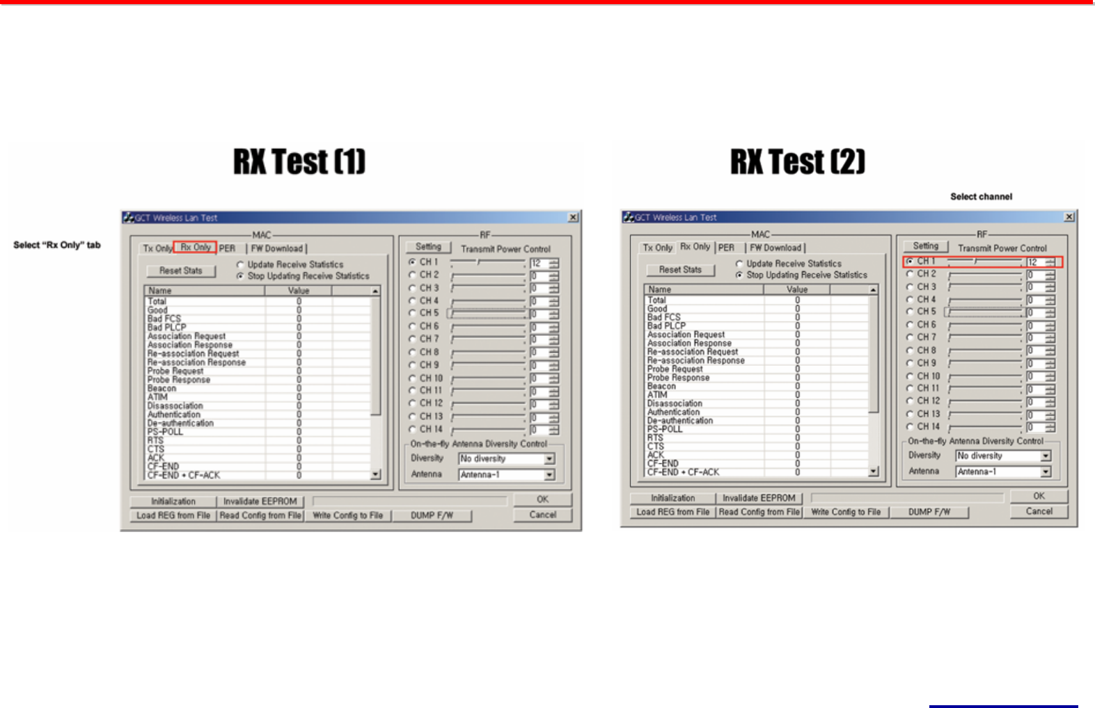
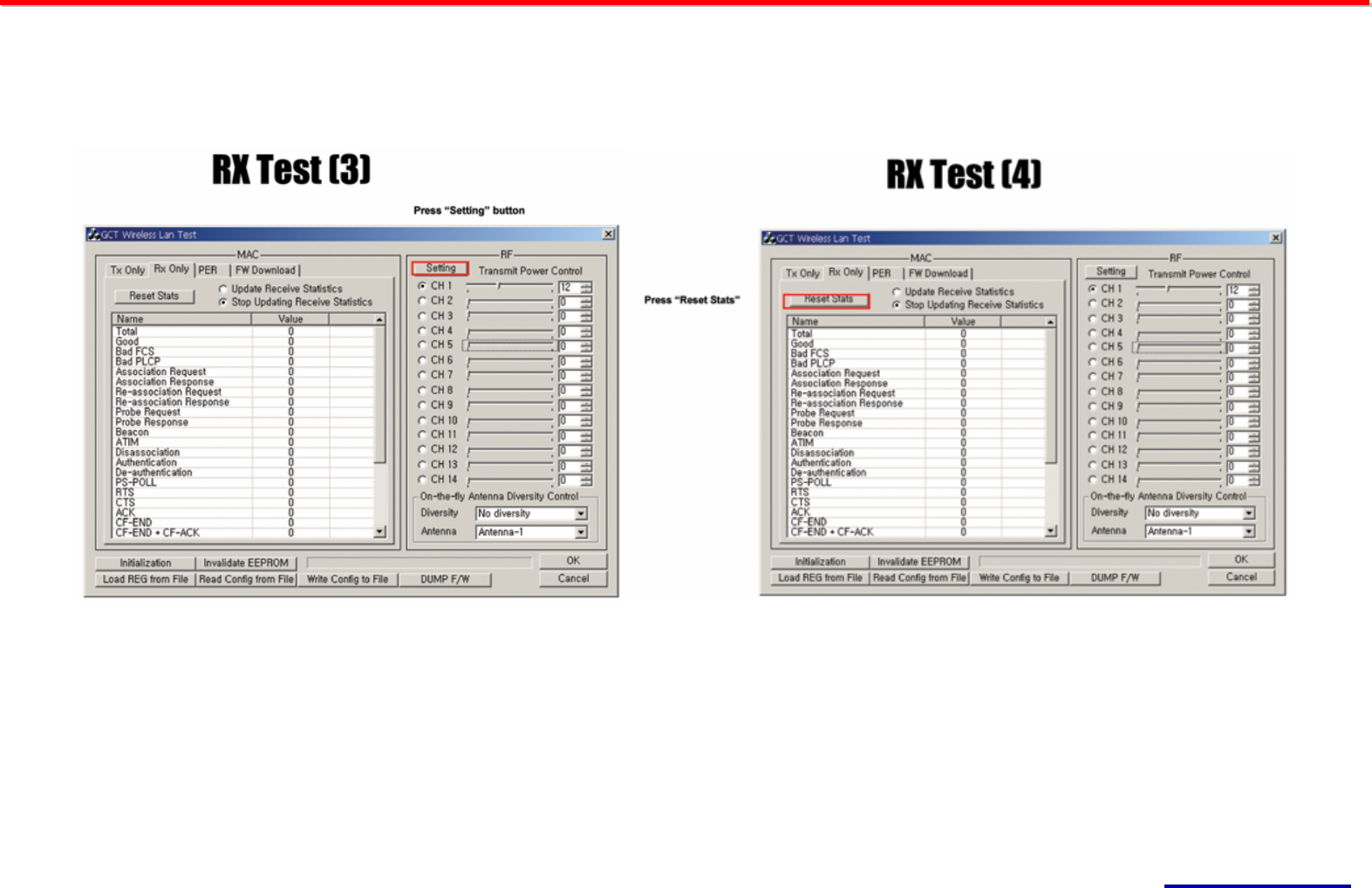
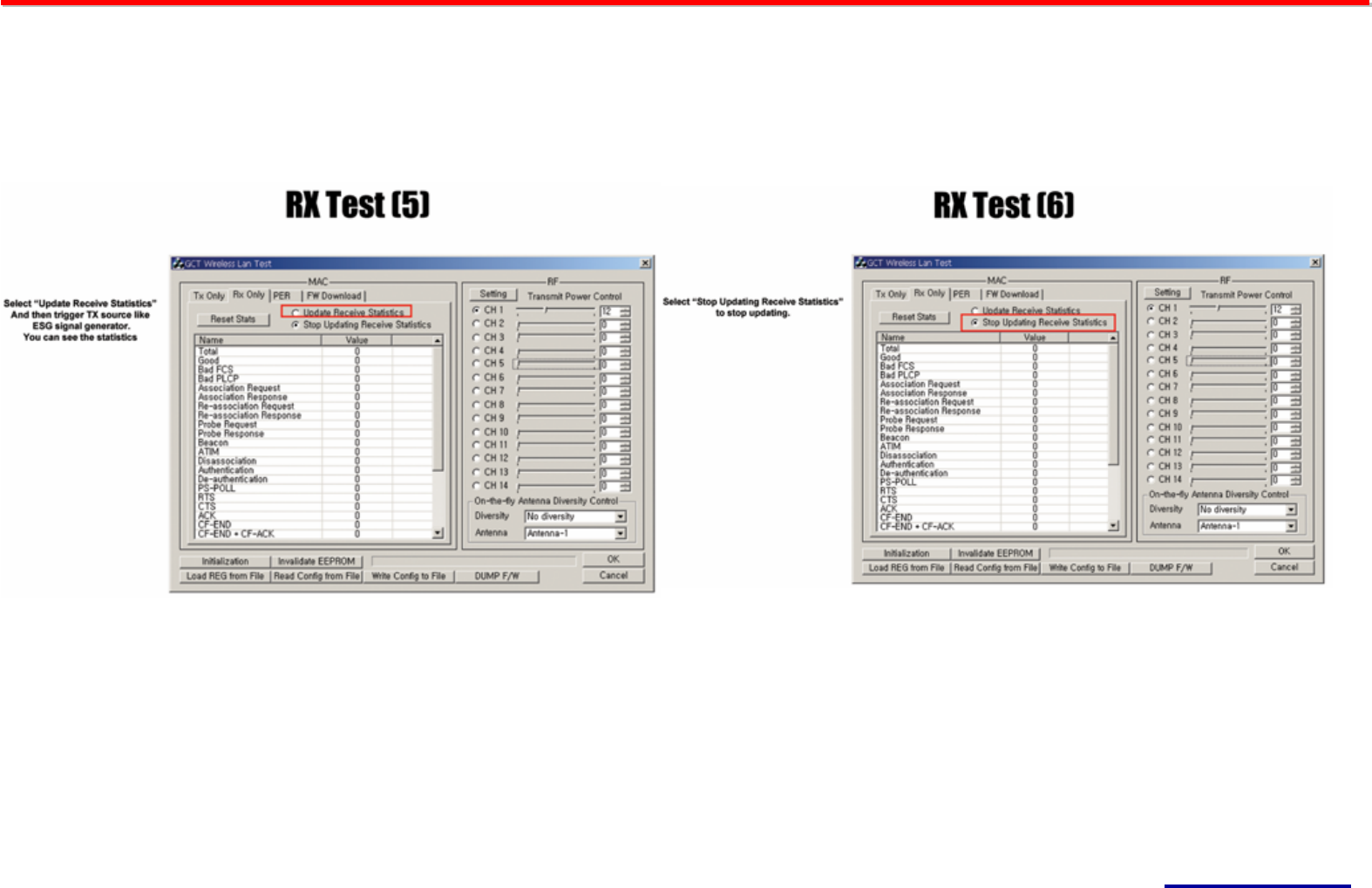
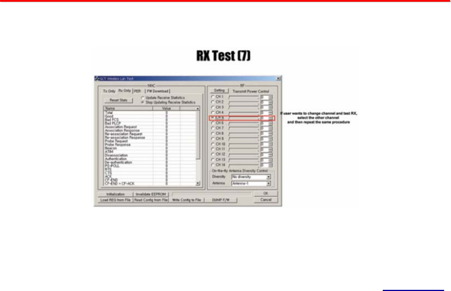
■ RX Test
1. Plug the power connector into Jig board including the module
2. Connect PC (or Notebook) with Jig board using USB cable
3. Power on Jig board
4. Make sure that PC (or NB) recognized the Jig board as a USB device
5. Initiate RF test utility on PC (or NB)
6. Start RF test
Contents
Environment Set-up
A
Au
ud
di
io
o
D
Da
at
ta
a
T
Tr
ra
an
ns
sc
ce
ei
iv
ve
er
r
R
RF
F
M
Mo
od
du
ul
le
e’
’s
s
M
Ma
an
nu
ua
al
l
VISION TECHNICS VWM-1G01A
VISION TECHNICS ©Copyrights 2005. All rights reserved
10
A
Au
ud
di
io
o
D
Da
at
ta
a
T
Tr
ra
an
ns
sc
ce
ei
iv
ve
er
r
R
RF
F
M
Mo
od
du
ul
le
e’
’s
s
M
Ma
an
nu
ua
al
l
VISION TECHNICS VWM-1G01A
VISION TECHNICS ©Copyrights 2005. All rights reserved
11
A
Au
ud
di
io
o
D
Da
at
ta
a
T
Tr
ra
an
ns
sc
ce
ei
iv
ve
er
r
R
RF
F
M
Mo
od
du
ul
le
e’
’s
s
M
Ma
an
nu
ua
al
l
VISION TECHNICS VWM-1G01A
VISION TECHNICS ©Copyrights 2005. All rights reserved
12
A
Au
ud
di
io
o
D
Da
at
ta
a
T
Tr
ra
an
ns
sc
ce
ei
iv
ve
er
r
R
RF
F
M
Mo
od
du
ul
le
e’
’s
s
M
Ma
an
nu
ua
al
l
VISION TECHNICS VWM-1G01A
VISION TECHNICS ©Copyrights 2005. All rights reserved
13
A
Au
ud
di
io
o
D
Da
at
ta
a
T
Tr
ra
an
ns
sc
ce
ei
iv
ve
er
r
R
RF
F
M
Mo
od
du
ul
le
e’
’s
s
M
Ma
an
nu
ua
al
l
VISION TECHNICS VWM-1G01A
VISION TECHNICS ©Copyrights 2005. All rights reserved
14
A
Au
ud
di
io
o
D
Da
at
ta
a
T
Tr
ra
an
ns
sc
ce
ei
iv
ve
er
r
R
RF
F
M
Mo
od
du
ul
le
e’
’s
s
M
Ma
an
nu
ua
al
l
VISION TECHNICS VWM-1G01A
VISION TECHNICS ©Copyrights 2005. All rights reserved
15
A
Au
ud
di
io
o
D
Da
at
ta
a
T
Tr
ra
an
ns
sc
ce
ei
iv
ve
er
r
R
RF
F
M
Mo
od
du
ul
le
e’
’s
s
M
Ma
an
nu
ua
al
l
VISION TECHNICS VWM-1G01A
VISION TECHNICS ©Copyrights 2005. All rights reserved
16
A
Au
ud
di
io
o
D
Da
at
ta
a
T
Tr
ra
an
ns
sc
ce
ei
iv
ve
er
r
R
RF
F
M
Mo
od
du
ul
le
e’
’s
s
M
Ma
an
nu
ua
al
l
VISION TECHNICS VWM-1G01A
VISION TECHNICS ©Copyrights 2005. All rights reserved
17
A
Au
ud
di
io
o
D
Da
at
ta
a
T
Tr
ra
an
ns
sc
ce
ei
iv
ve
er
r
R
RF
F
M
Mo
od
du
ul
le
e’
’s
s
M
Ma
an
nu
ua
al
l
VISION TECHNICS VWM-1G01A
VISION TECHNICS ©Copyrights 2005. All rights reserved
18
A
Au
ud
di
io
o
D
Da
at
ta
a
T
Tr
ra
an
ns
sc
ce
ei
iv
ve
er
r
R
RF
F
M
Mo
od
du
ul
le
e’
’s
s
M
Ma
an
nu
ua
al
l
VISION TECHNICS VWM-1G01A
VISION TECHNICS ©Copyrights 2005. All rights reserved
19
A
Au
ud
di
io
o
D
Da
at
ta
a
T
Tr
ra
an
ns
sc
ce
ei
iv
ve
er
r
R
RF
F
M
Mo
od
du
ul
le
e’
’s
s
M
Ma
an
nu
ua
al
l
VISION TECHNICS VWM-1G01A
VISION TECHNICS ©Copyrights 2005. All rights reserved
20
A
Au
ud
di
io
o
D
Da
at
ta
a
T
Tr
ra
an
ns
sc
ce
ei
iv
ve
er
r
R
RF
F
M
Mo
od
du
ul
le
e’
’s
s
M
Ma
an
nu
ua
al
l
VISION TECHNICS VWM-1G01A
VISION TECHNICS ©Copyrights 2005. All rights reserved
21

A
Au
ud
di
io
o
D
Da
at
ta
a
T
Tr
ra
an
ns
sc
ce
ei
iv
ve
er
r
R
RF
F
M
Mo
od
du
ul
le
e’
’s
s
M
Ma
an
nu
ua
al
l
VISION TECHNICS VWM-1G01A
VISION TECHNICS ©Copyrights 2005. All rights reserved
22
4. Product specification
Transmit frequency : 2400 ~ 2483.5 MHz
Antenna Power : 9.5dBm(W/Ant.Gain & Cable Loss)
Channel : 13 Ch
Supply voltage : DC +3.3V
Size : 43 x 10 x 60 (W x H x D)
Weight : 13 g
Operating temperature : 0 ~ +35℃
Modulation system : DSSS (CCK, DQPSK, DBPSK)
Oscillation System : Synthesizer operation
Type of emission : G1D
Communication method : Semiduplex operation
A
Au
ud
di
io
o
D
Da
at
ta
a
T
Tr
ra
an
ns
sc
ce
ei
iv
ve
er
r
R
RF
F
M
Mo
od
du
ul
le
e’
’s
s
M
Ma
an
nu
ua
al
l
VISION TECHNICS VWM-1G01A
VISION TECHNICS ©Copyrights 2005. All rights reserved
23
A
Au
ud
di
io
o
D
Da
at
ta
a
T
Tr
ra
an
ns
sc
ce
ei
iv
ve
er
r
R
RF
F
M
Mo
od
du
ul
le
e’
’s
s
M
Ma
an
nu
ua
al
l
VISION TECHNICS VWM-1G01A
VISION TECHNICS ©Copyrights 2005. All rights reserved
24
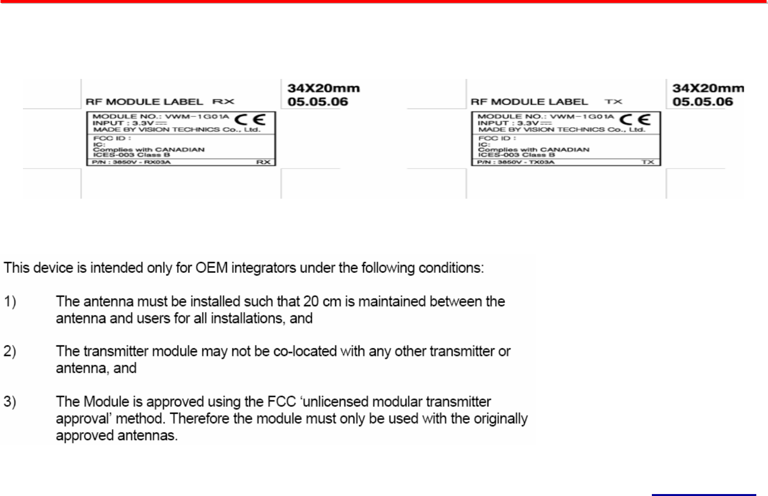
5. LABEL
<Size>
6.Regulatory Information
A
Au
ud
di
io
o
D
Da
at
ta
a
T
Tr
ra
an
ns
sc
ce
ei
iv
ve
er
r
R
RF
F
M
Mo
od
du
ul
le
e’
’s
s
M
Ma
an
nu
ua
al
l
VISION TECHNICS VWM-1G01A
VISION TECHNICS ©Copyrights 2005. All rights reserved
25
A
Au
ud
di
io
o
D
Da
at
ta
a
T
Tr
ra
an
ns
sc
ce
ei
iv
ve
er
r
R
RF
F
M
Mo
od
du
ul
le
e’
’s
s
M
Ma
an
nu
ua
al
l
VISION TECHNICS VWM-1G01A
VISION TECHNICS ©Copyrights 2005. All rights reserved
26