WiSilica WISE1230 BLE Module User Manual users manual
WiSilica, Inc. BLE Module users manual
WiSilica >
users manual

WiSe 1230BLE Module Technical Specification
WiSilica Inc
WiSe 1230 Hardware and Technical Specification
Version (Rev 1.5)
Issued: 14/06/2017

WiSe 1230BLE Module Technical Specification
WiSilica Inc
Table of Contents
General Information ............................................................................................................................... 4
Features .............................................................................................................................................. 4
General Description ............................................................................................................................ 4
Block Diagram: ........................................................................................................................................ 4
Application: ............................................................................................................................................. 5
Form factor: ............................................................................................................................................ 5
Hardware Specification: .......................................................................................................................... 5
Antenna ................................................................................................................................................... 5
Pinout and Pin Description ..................................................................................................................... 6
Pinout Diagram ................................................................................................................................... 6
Electrical characteristics.......................................................................................................................... 7
Absolute Maximum Ratings ................................................................................................................ 7
Recommended operating condition ................................................................................................... 7
AIO ...................................................................................................................................................... 7
PWM ....................................................................................................................................................... 7
Current Consumption: ............................................................................................................................ 7
RF Characteristics: ................................................................................................................................... 8
Host details: ............................................................................................................................................ 9
Multisensor ......................................................................................................................................... 9
Smart lighting device........................................................................................................................... 9
Best practices .................................................................................................................................... 10

WiSe 1230BLE Module Technical Specification
WiSilica Inc
Revision History
Rev No
Date
Notes
Rev 1.0
05/01/2017
Draft Release
Rev 1.1
07/02/2017
BLE chip partnumber corrected
Rev1.2
14/02/2017
Block diagram and External antenna guide included.
Rev1.3
23/02/2017
Land Pattern Dimension added.
Rev1.4
17/04/2017
PCB Antenna description removed.
Rev1.5
14/06/17
Module Host details added.
WiSe 1230BLE Module Technical Specification
WiSilica Inc
General Information
Features
Bluetooth v4.0 specification complaint
Support for Bluetooth 4.1 specification host stack
512KB of Flash memory
12 MHz and 32MHz clock system
PWM/SPI/GPIO/UART/I2C interface
TX output power upto +5dbm
-92dbm BT4.0 RX sensitivity
RSSI Monitoring
5 programmable GPIO’s/ 5 PWM channels
2 AIO channels
General Description
WiSe 1230 module enables ultra-low-power connectivity and basic data transfer for applications
previously limited by the power consumption, size constraints and complexity of other wireless
standards.WiSe 1230 is intended to provide considerably reduced power consumption and cost.
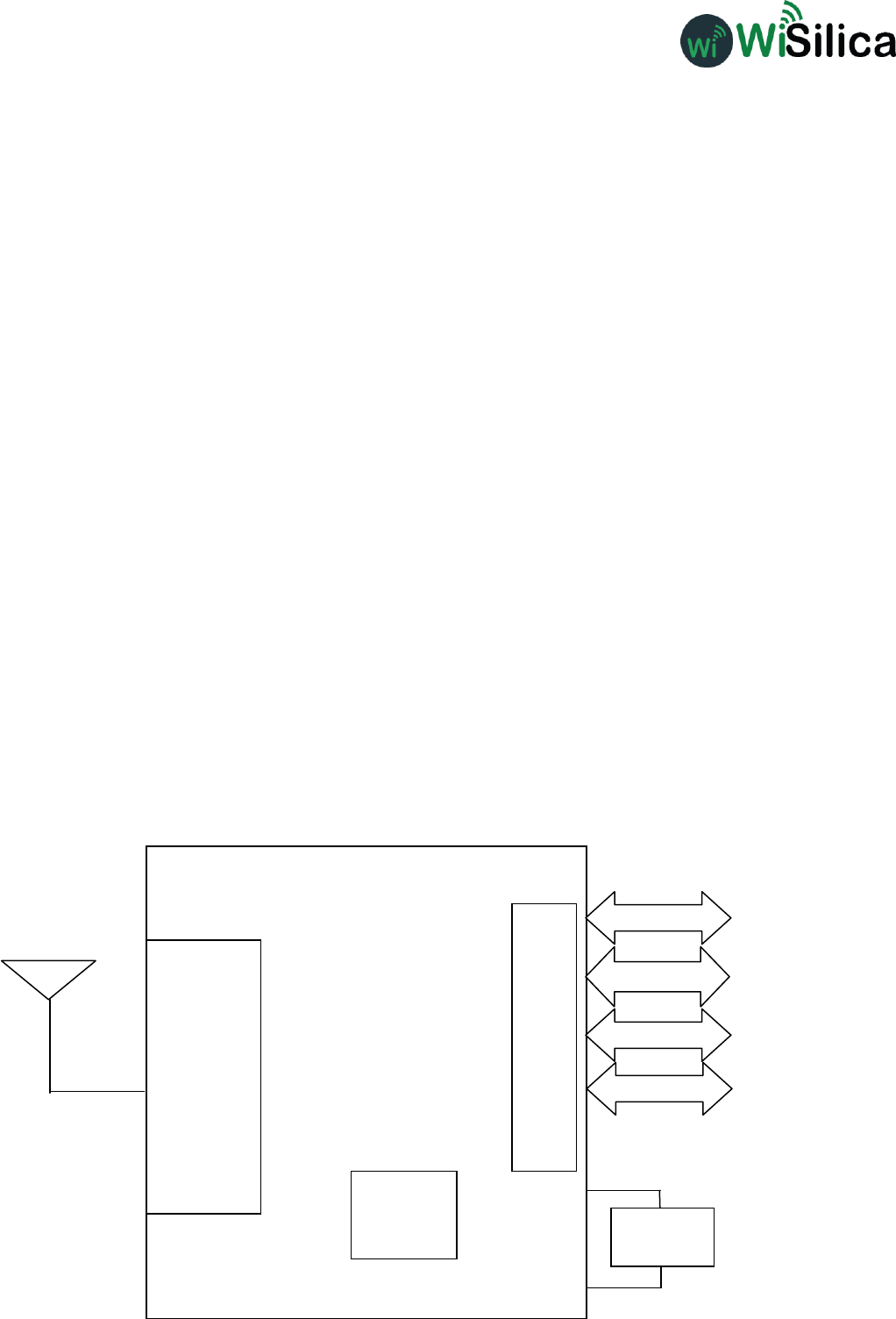
Block Diagram:
TLSR8269F512AT32
GPIO
CRYSTAL
12MHz
IO
512KB
FLASH
PWM
I2C
DMIC
2.4GHz
Radio

WiSe 1230BLE Module Technical Specification
WiSilica Inc
Application:
WiSe 1230 enables connectivity and data transfer to leading smartphone, tablet and personal
computing devices including Apple iPhone, iPad, iPod and Mac products and leading Android devices.
Smart mesh light application
Smart home heating and lighting control
Health sensors like blood pressure, thermometer and glucose meter
Beacons
Security
Sensors
Wearable devices.
Form factor:
Dimension: 23.45x15mm
Hardware Specification:
COMPONENTS
DESCRIPTION
BLE CHIP
TLSR8269F512AT32
CRYSTAL
12MHz
External antenna.
Antenna
WiSe1230 Modules has external antenna with UFL connector.The WiSe1230 has been certified with
the external antenna only.
The external antenna’s directivity determines the required position and orientation of the antenna
with respect to the ground plane. We need to make sure the external antenna impedance is close
to 50 Ohm to have optimal matching. External antenna’scentreband frequency should be in the
range of 2.4 to 2.483 GHz.The nearby materials and nature of the application determine whether
you need a directional or omnidirectional antenna.
The following are some design guidelines to help ensure antenna performance:
Never place the ground plane or route copper traces directly underneath the antenna
portion of the module.
Never place the antenna close to metallic objects.
In the overall design, ensure that wiring and other components are not placed near the
antenna.
Do not place the antenna in a metallic or metalized plastic enclosure.
WiSe 1230BLE Module Technical Specification
WiSilica Inc
Keep plastic enclosures 1cm or more away from the antenna in any direction.Description
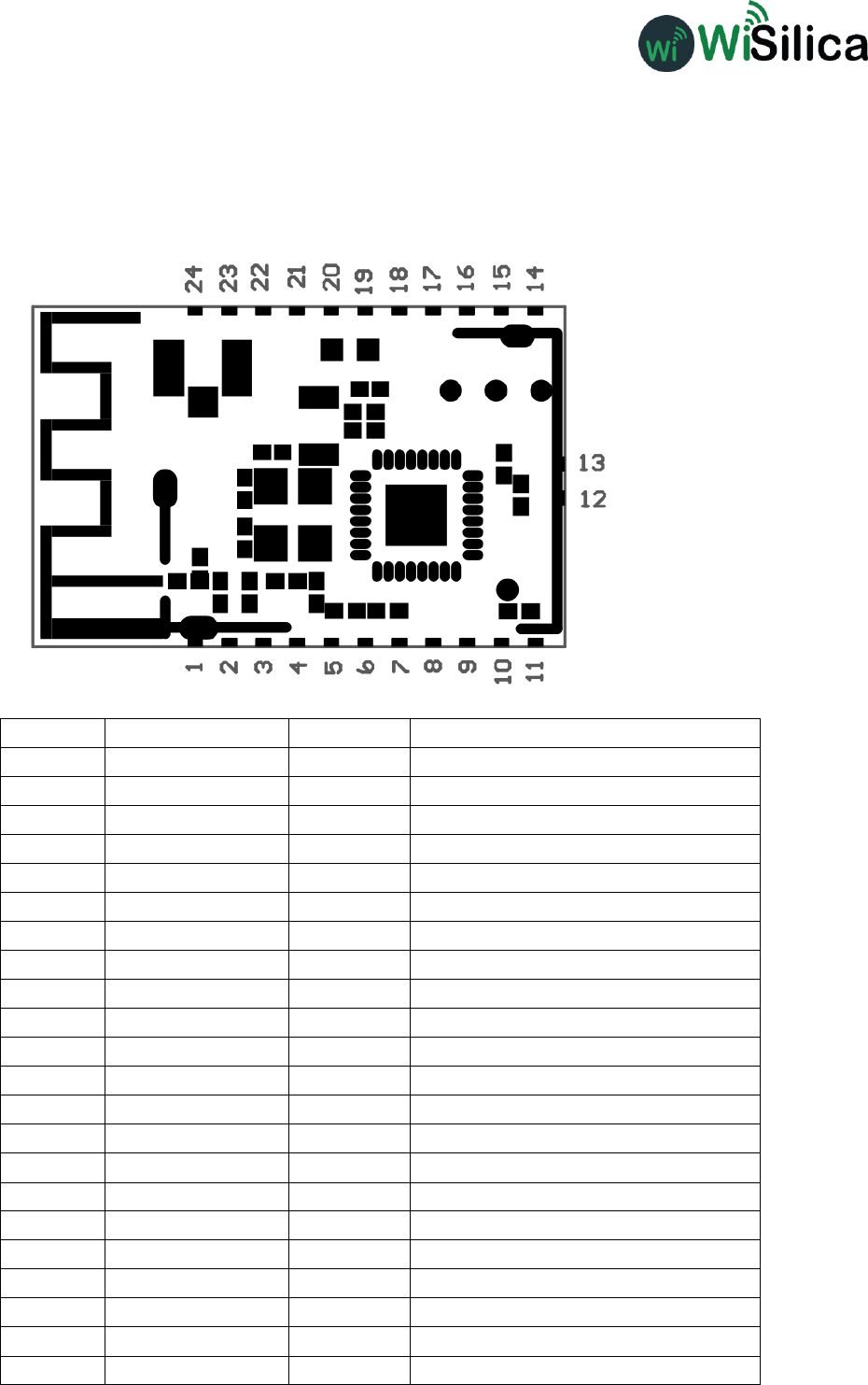
Pinout and Pin Description
Pinout Diagram
PINS
NAME
FUNCTION
COMMENTS
1
GND
Ground
Ground(Vss)
2
ANA_B1
I/O
Programmable I/O or AIO
3
ANA_B0/SWS
I/O or AIO
Programmable I/O or AIO
4
GP5
I/O or AIO
Programmable I/O or AIO
5
TX
I/O
Programmable I/O
6
RX
I/O
Programmable I/O
7
PWM1
I/O or AIO
Programmable I/O or AIO
8
SPI_CLK
I
SPI Clock or Programmable I/O
9
DP/IO
I/O
Programmable I/O
10
DMIC_DI/A0
I/O
DMIC data I/P or Programmable I/O
11
DMIC_CLK/A1
I/O
DMIC Clk or Programmable I/O
12
GND
Ground
Ground(Vss)
13
GND
Ground
Ground(Vss)
14
SWM/A7
I/O
Single Wire Master or I/O
15
I2C_SDA
I/O
I2C Data or Programmable I/O
16
I2C_SCL
I/O
I2C Clk or Programmable I/O
17
PWM5
I/O
Programmable I/O
18
PWM4
I/O
Programmable I/O
19
PWM0
I/O
Programmable I/O
20
VDD33
Power
Power Input(Vdd)
21
GP4/D2
I/O
Programmable I/O
22
CSB
O
SPI select or Programmable I/O
WiSe 1230BLE Module Technical Specification
WiSilica Inc
23
SPI_MISO
O
SPI data output or Programmable I/O
24
SPI_MOSI
I
SPI data input or Programmable I/O
Electrical characteristics
Absolute Maximum Ratings
Ratings
Min
Max
Storage Temperature
-65°C
125°C
Supply voltage
2.2V
3.6V
Recommended operating condition
Item
Min
Typical
Max
Operating Temperature
-40
-
125°C
Supply voltage
2.2V
3.3V
3.6V
IO Supply Voltage
V
-
3.6V
AIO
Ratings
Min
Max
Input Voltage
0.7
3.3V
Output voltage
V
3.3V
PWM
Totally there are 5 PWM channels.
PWM Frequency: Target frequency TBD kHz.
Maximum voltage for logic low: VIL = 0 V
Absolute maximum current sourced: IMAX = mA
Absolute maximum voltage level: VMax =3.6V
Current Consumption:
Mode
Total Typical Current at 3V
Sleep Mode
15μA
RX/TX active
~15mA @ 3V peak current
WiSe 1230BLE Module Technical Specification
WiSilica Inc
RF Characteristics:
Path
Description
Conditions
Min
Typ
Max
Unit
Operating Frequency
2402
2480
MHz
Maximum output power
7
dBm
2nd harmonic
54
dBuV
3rd harmonic
54
dBuV
TX
Modulation delta F1 average
225
255
275
kHz
Modulation delta F1 / F2
0.8
Modulation delta F2 max
100
%
Frequency accuracy
-100
25
100
kHz
Frequency offset
-100
25
100
kHz
RX
Receiver Sensitivity
-92
dBm
Receiver Sensitivity (with dirty transmitter)
-93
dBm
Maximum received signal at 30.8% PER
-10
dBm
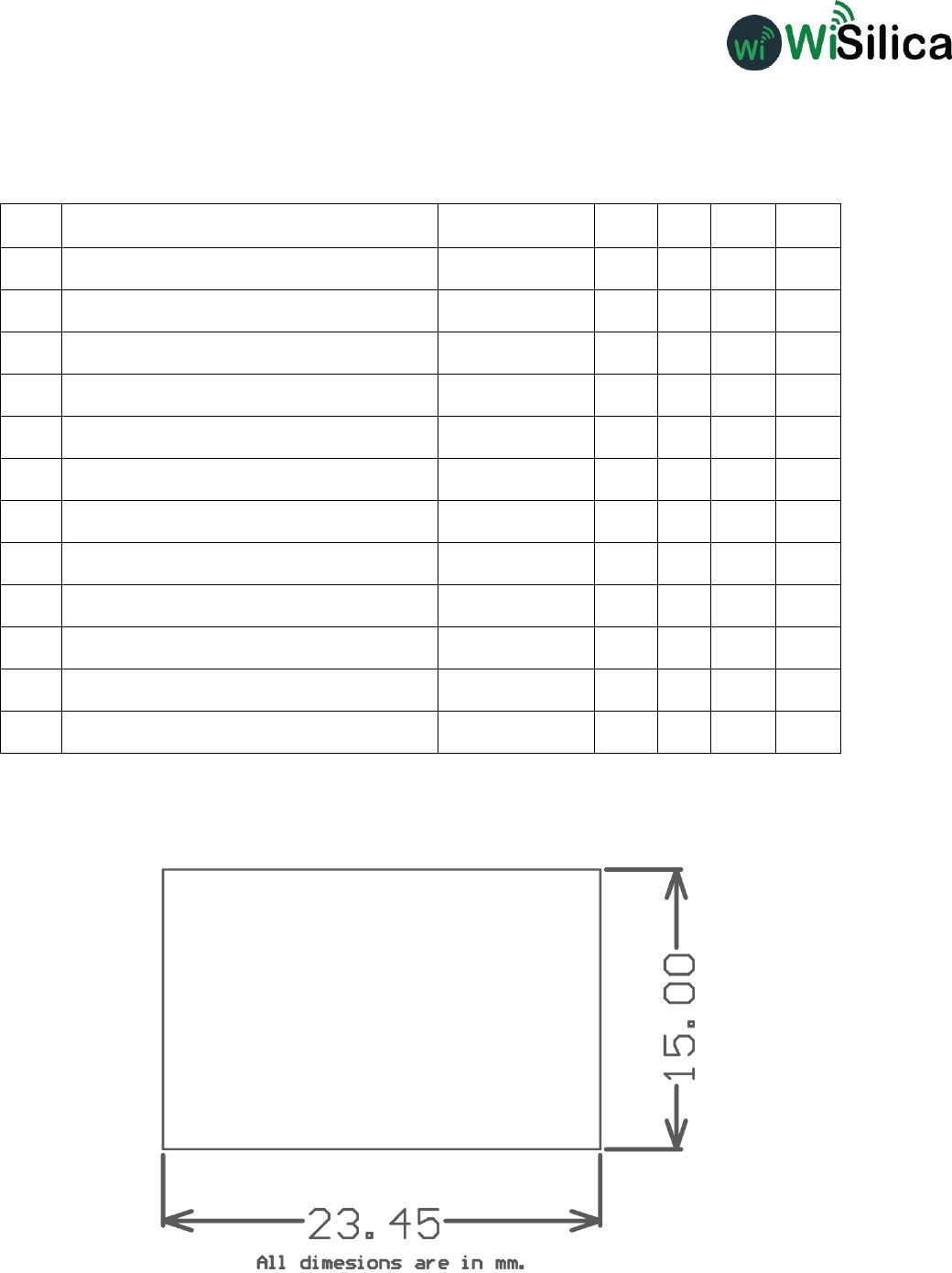
Module Dimension
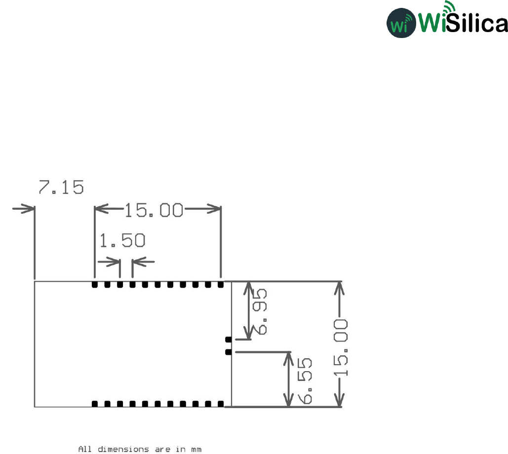
WiSe 1230BLE Module Technical Specification
WiSilica Inc
Recommended Land Pattern Dimension:
Dimension: 23.45x15mm
Pitch: 1.5mm
Pad dimension: 0.96x0.96mm
Height:3.4mm(includes shield)
Host details:
The WiSe1230 module is going to be embedded with Multisensor
Multisensor
Multisensor is the one which contains PIR (ALS312), LDR (TEMT6000)RTC (HYM8563) and
WiSe1230 module. It is intended to be a general purpose remote control that contains PIR,
Ambient light sensor, Real time clock. Eventually we can make this an extremely flexible device
by combining the PIR and ambient light sensor functions into one, and use the real-time clock to
send out time sync packets for the low-power mesh.Also it can be used as a scheduler.
Also this device is the 2 x AAA battery powered.
Note: The module can be integrated only in the host plattform where it has been tested. Any
additional hosts having different function, shape and electrical characteristics should be added
with a class 2 permissive change. This implies additional testing of the radiated emissions within
the new host.

WiSe 1230BLE Module Technical Specification
WiSilica Inc
Best practices
When designing with WiSe1230 modules, please pay attention to the following recommendations
While integrating module make sure all the module pads are soldered properly.
The module's voltage requirement is 2.5 to 3.6V, if the power supply is over 3.3V, please
use a voltage regulator.
If the communicating host uses a different voltage then the BLE module, please make
sure that the voltage matches on the communication ports.
The external antenna needs to be connected to the module.
For best wireless signals, please avoid packing the antenna close to metal parts or case.
Integrator is reminded to assure that these installation instructions
will not be made available to the end
-
user of the final host device.
The final host device, into which this RF Module isintegrated" hasto be labelled
with an auxilliary lable stating the FCC IDofthe RF Module,
such as "Contains FCC ID: 2AG4NWISE1230"
"This device complies with part 15 of the FCC rules. Operation is subject to the following two
conditions:
(1)this devicemay not cause harmful interference, and
(2)this devicemust accept any interference received, including
interference thatmay cause undesired operation."
NOTE: This equipment has been tested and found to comply with the limits for a Class B digital
device, pursuant to part 15 of the FCC Rules. These limits are designed to provide reasonable
protection
against harmful interference in a residential installation. This equipment generates, uses and can
radiate radio frequency energy and, if not installed and used in accordance with the instructions,
may cause harmful interference to radio communications. However, there is no guarantee that
interference will not occur in a particular installation. If this equipment does cause harmful
interference to radio or television reception, which can be determined by turning the equipment
off and on, the user is encouraged to try to correct the interference by one or more of the
following measures:
--Reorient or relocate the receiving antenna.
--Increase the separation between the equipment and receiver.
--Connect the equipment into an outlet on a circuit different from that to which the receiver is
connected.
--Consult the dealer or an experienced radio/TV technician for help.
Changes or modifications to this unit not expressly approved by the party responsible for
compliance could void the user's authority to operate the equipment.
(OEM) Integrator has to assure compliance of the entire end-product incl. the integrated RF Module.
For 15 B (§15.107 and if applicable §15.107) compliance, the host manufacturer is required to
show compliance with 15 while the module is installed and operating.
Furthermore the module should be transmitting and the evaluation should confirm that the module's
intentional emissions (15C) are compliant (fundamental / out-of-band). Finally the integrator has
to apply the appropriate equipment authorization (e.g. Verification) for the new host device per
definition in §15.101.