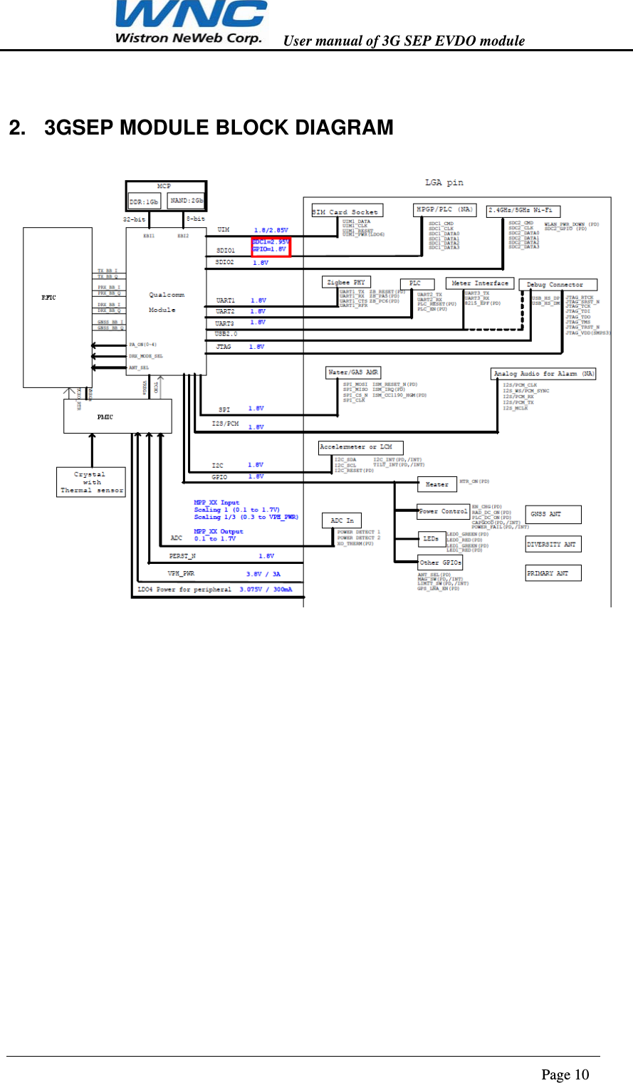
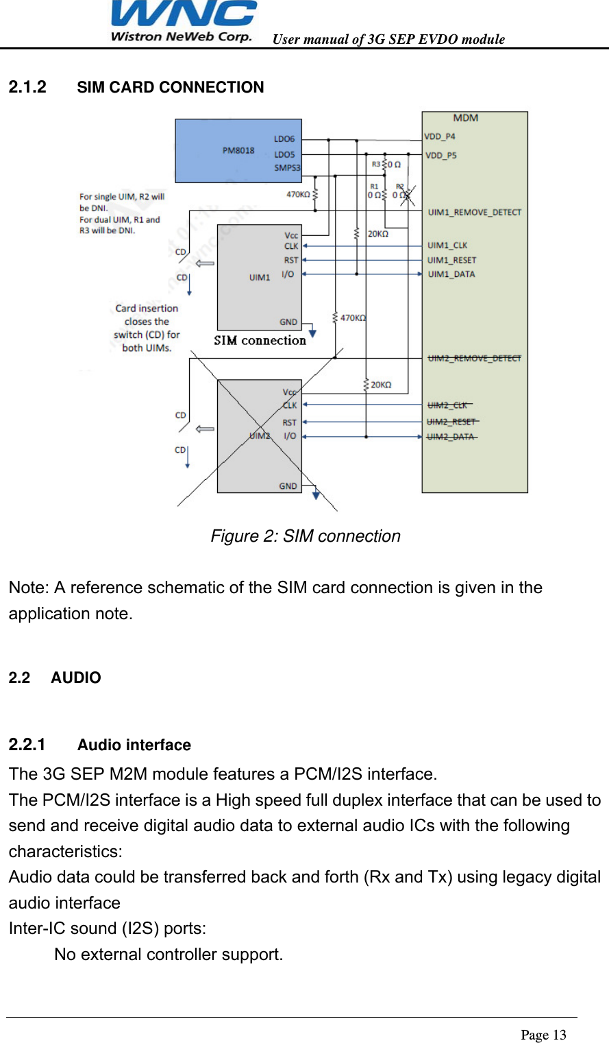
Wistron NeWeb 96E1 3G SEP EVDO LGA MODULE User Manual
Wistron NeWeb Corporation 3G SEP EVDO LGA MODULE
UserManual.wiki
>
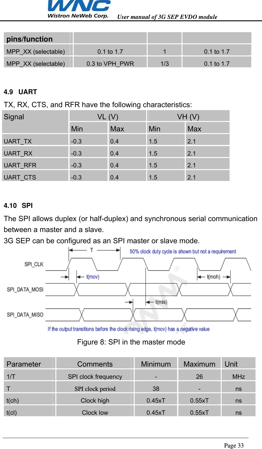
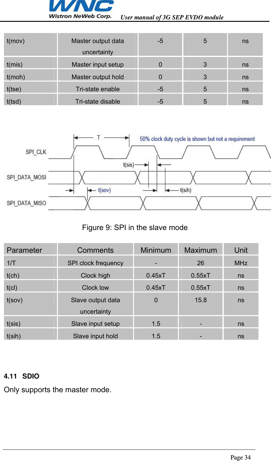
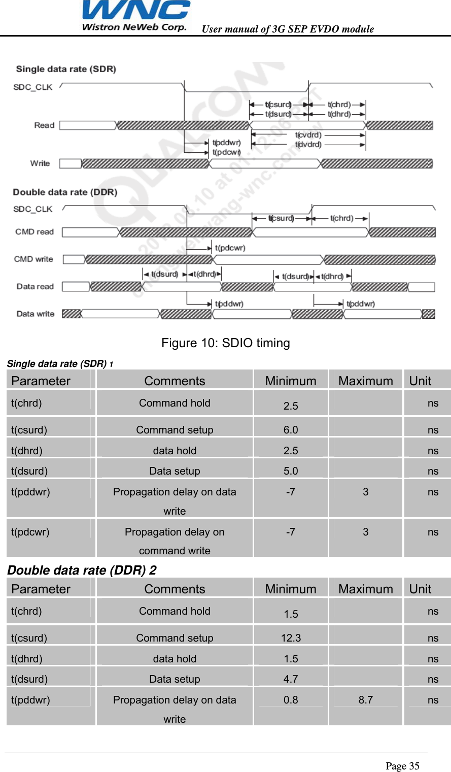
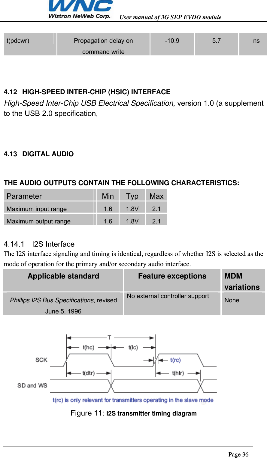
Wistron NeWeb
>
96E1 User Manual
User Manual
Navigation menu
Upload a User Manual
Namespaces
Wiki Guide
HTML
PDF
Info
Views
User Manual
Discussion / Help
Navigation