Wistron NeWeb 96E1 3G SEP EVDO LGA MODULE User Manual
Wistron NeWeb Corporation 3G SEP EVDO LGA MODULE
User Manual

User manual of 3G SEP EVDO module
Page 1
Wistron NeWeb Corp.
啟碁科技股份有限公司
User manual of
3G SEP Module
(EVDO version)

User manual of 3G SEP EVDO module
Page 2
Revision History
Version Change history Date
Ver 0.1 Initial version 2012-10-15
Ver 0.2 Update EVDO 2013-1-16
Ver 0.3 Update IO spec 2013-1-22
Ver 0.4 Update FCC/IC warning
statement 2013-5-16
Ver 0.5 Modify 6.4 FCC Module
Integration Restriction 2013-5-29

User manual of 3G SEP EVDO module
Page 3
Contents
Contents........................................................................................................................ 3
1.introduction ............................................................................................................ 5
1.1productconcept.........................................................................................5
1.2Termsandabbreviation.............................................................................5
1.3Conventions...............................................................................................7
1.4Productfeaturesoverview.........................................................................7
2.3GSEP Module Block diagram ............................................................................ 10
2.1SIM...........................................................................................................12
2.2AUDIO.......................................................................................................13
2.3High‐speedinter‐chip(HSIC)Interface....................................................18
2.4GeneralpurposeI/O................................................................................18
2.5RESET........................................................................................................19
2.6ADC...........................................................................................................19
PowerOUTPUT.....................................................................................................19
2.7POWERSUPPLY&GND............................................................................19
2.8POWERMANAGEMENT...........................................................................20
2.9Sleepmodes.............................................................................................20
2.10RTCfuncution...........................................................................................22
3.Pinout ................................................................................................................... 23
3.1I/OConnectorPinAssignments...............................................................23
4.Electrical specificationS ....................................................................................... 30
4.1VPHPwr...................................................................................................30
4.2Vbackup....................................................................................................30
4.3VSIM.........................................................................................................31
4.4Digitalinterface........................................................................................31
4.5RESET........................................................................................................31
4.6SIM...........................................................................................................32
I2CInterfacE.........................................................................................................32
I2Chasthefollowingcharacteristics:..................................................................32
4.7USB...........................................................................................................32

User manual of 3G SEP EVDO module
Page 4
4.8ADC...........................................................................................................32
4.9UART.........................................................................................................33
4.10SPI.............................................................................................................33
4.11SDIO..........................................................................................................34
4.12High‐speedinter‐chip(HSIC)interface....................................................36
4.13DIGITALAUDIO.........................................................................................36
Theaudiooutputscontainthefollowingcharacteristics:...................................36
4.14RFSIGNAL.................................................................................................40
5.Environmental specificationS .............................................................................. 41
5.1NormaltemperatureRange.....................................................................41
5.2ExtendedtemperatureRange..................................................................42
6.FCC warning statement ........................................................................................ 43
6.1General.....................................................................................................43
6.2EndProductLabeling(FCC)......................................................................43
6.3RequiredFCCComplianceStatementforHostIntegration.....................43
6.4FCCModuleIntegrationRestriction:........................................................44

User manual of 3G SEP EVDO module
Page 5
1. INTRODUCTION
This document describes the specifications of the WNC 3G SEP M2M module
used to connect the device application and the air interface.
1.1 PRODUCT CONCEPT
The 3G SEP module provides CDMA connectivity for machine-to-machine
(M2M) application over dual frequency bands BC0 and BC1. The markets of
application include AMM (Automatic Metering Management), tracking system,
and alarm, etc.
Application and physical features:
Operating temperature range: -30°C to +85°C
Interface and dimension: LGA; 34X34mm
Minimum low power consumption in the standby mode: 1.5mA
DC supply: 3.4 V to 4.2 V
USB2.0 high speed
Supported frequency bands:
BC0
BC1
In addition to the 3G SEP module, a complete development kit can be provided
to customers.
1.2 TERMS AND ABBREVIATION
ADC Analog to Digital Converter
CDMA Code Division Multiple Access
CODEC Coder-Decoder
CLIP Calling Line Identification Presentation
COLP Connected Line Identification Presentation
CLIR Calling Line Identification Restriction
COLR Connected Line Identification Restriction
CTS Clear To Send
CSD Circuit Switched Data

User manual of 3G SEP EVDO module
Page 6
CS Coding Scheme
DCS Digital Communications System
DSR Data Set Ready
DTR Data Terminal Ready
EDGE Enhanced Data Rate for GSM Evolution
EGSM Extended GSM
ENS Enhanced network selection
EONS Enhanced operator name string
ESD Electrostatic Discharge
ETS European Telecommunication Standard
GNSS Global Navigation Satellite System
GSM Global System for Mobile communication
GPRS General Packet Radio Services
GPS Global Positioning System
HSCSD High Speed Circuit Switched Data
HSDPA High Speed Downlink Packet Access
HSIC High-speed inter-chip
HSPA+ Evolved High-Speed Packet Access
HSUPA High Speed Uplink Packet Access
IC Integrated Circuit
IEEE Institute of Electrical and Electronics Engineers
I/O Input / Output
ISO International Standards Organization
ITU International Telecommunication Union
I2C Inter-integrated circuit
I2S Inter-IC sound
JTAG Joint Test Action Group
Kbps kilobit per second
LCD Liquid Crystal Display
LED Light Emitting Diode
LTE Long term evolution
Mbps Megabit per second
PA Power amplifier
PBCCH Packet Broadcast Control Channel
PCB Printed Circuit Board

User manual of 3G SEP EVDO module
Page 7
PCM Pulse Code Modulation
PCS Personal Communication System
PMIC Power management integrated circuit
PWM Pulse Width Modulation
RAM Random Access Memory
RF Radio Frequency
RI Ring Indication
RMS Root Mean Square
RTS Ready To Send
RX Reception
SIM Subscriber Identification Module
SMS Short Message Service
TBC To Be Confirmed
TBD To Be Defined
TCXO Temperature-compensated crystal oscillator
TX Transmission
UART Universal Asynchronous Receiver and Transmitter
UIM User identity module
UMTS Universal Mobile Telecommunications System
USB Universal Serial Bus
USSD Unstructured Supplementary Service Data
WCDMA Wideband Code Division Multiple Access
1.3 CONVENTIONS
Throughout this document, DTE (data terminal equipment) indicates the
equipment which masters and controls the module device UMC-3GSEP by
sending AT commands via its serial interface.
DCE (data communication equipment) indicates the UMC-3GSEP module
device.
1.4 PRODUCT FEATURES OVERVIEW

User manual of 3G SEP EVDO module
Page 8
Mechanical & environment
Temperature range Normal range: -30°C to +70°C (fully compliant)
Extended range: -30°C to +85°C (fully functional)
Storage: -40°C to +105°C
Weight (g) 6 grams
ESD ESD protection :+/- 2 kV
Physical dimensions 34x34x3 mm
Connection 157 pins LGA contact
Power supply 3.4V to 4.2V range, 4.0V nominal
Power consumption1 Off mode: 50 µA typical
Registered idle mode: (cell power -55dBm/1.23MHz)
CDMA: 200mA
Peak Current
CDMA: up to 780mA
Cellular technologies
CDMA bands BC0 : Tx: 824–849 MHz; Rx: 869–894 MHz
BC1 : Tx: 1850–1910 MHz; Rx: 1930–1990 MHz
Transmit power 24dBm+/-1dB
Main interfaces
1Thepowerconsumptionishighlydependentonthecustomer’sproductdesignandthemodule
environment.
User manual of 3G SEP EVDO module
Page 9
USB Supports USB High speed 480Mbps and full speed
12Mbps, with 3 logical Channels.
UART interface with flow
control
Up to 3.6 Mbit/s for data transmission (no auto-bauding)
Full flow control signals (+1.8V) are provided on a 94 pins
LGA connector.
A reference schematic to build the RS232 interface is
provided in the UMC-3GSEP application note.
Supported SIM cards 3V and 1.8V SIM cards
SIM slot Signals for the management of the SIM card are provided
on LGA pins.
SIM detect Provides SIM card insert detection.
General purpose I/O pins GPIOs can be customized easily from the customer’s
application and they can be configured as input or output
Power on pin Available
Audio
Digital audio link A digital audio interface PCM/I2S bus is provided.
Voice codec Half Rate, Full Rate, Enhanced Full Rate, Adaptive Multi
Rate
Data/command multiplexing Software management of data/command multiplexing on
the serial link UART.
Data services
1xEV-DOrA High-speed peak data rates – 3.1 Mbps forward link; 1.8
Mbps reverse link
User manual of 3G SEP EVDO module
Page 10
2. 3GSEP MODULE BLOCK DIAGRAM
User manual of 3G SEP EVDO module
Page 11
Figure 1: 3G SEP Pin-out (Top view)
User manual of 3G SEP EVDO module
Page 12
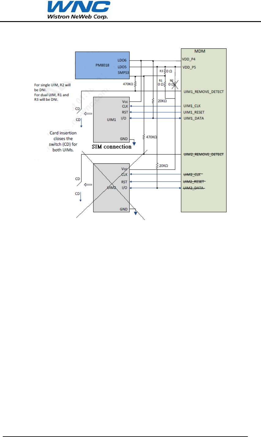
2.1 SIM
2.1.1 SIM card interface
The SIM Card Interface is compatible with the ISO 7816-3 IC card standard on
the issues required by the GSM 11.11 Phase 2+ standard and adapts to 3V
and 1.8V SIM cards.
To prevent SIM card damage, the power supply of the module must be turned
off before any manipulation of the SIM card.
The SIM card interface includes:
Power supply output (LDO6)
Bi-direction data signal (UIM1_DATA),
Clock output (UIM1_CLK)
Reset signal (UIM1_RESET)
Signal Pin N° Description
UIM1_RESET 26 SIM reset, provided by Base-band processor
UIM1_CLK 90 SIM clock, provided by Base-band processor
LDO6 91 SIM supply voltage
UIM1_DATA 27 SIM serial data line, input and output
User manual of 3G SEP EVDO module
Page 13
2.1.2 SIM CARD CONNECTION
Figure 2: SIM connection
Note: A reference schematic of the SIM card connection is given in the
application note.
2.2 AUDIO
2.2.1 Audio interface
The 3G SEP M2M module features a PCM/I2S interface.
The PCM/I2S interface is a High speed full duplex interface that can be used to
send and receive digital audio data to external audio ICs with the following
characteristics:
Audio data could be transferred back and forth (Rx and Tx) using legacy digital
audio interface
Inter-IC sound (I2S) ports:
No external controller support.
User manual of 3G SEP EVDO module
Page 14
Pulse-code modulation (PCM) audio ports:
Fixed sampling rate at 8 kHz
8 bits A-Law or µ-Law
16 bits linear PCM
PCM master mode
Fixed PCM clock rate at 128 kHz or 2.048 MHz
PCM slave mode
Fixed PCM clock rate at 2.048 MHz only
Signal Pin N° Description
I2S/PCM_CLK 113 I2S/PCM clock signal
I2S_WS/PCM_SYNC 49 I2S word select/ PCM sync signal
I2S/PCM_RX 115 I2S/PCM data input
I2S/PCM_TX 50 I2S/PCM data output
I2S_MCLK 114 I2S master clock
2.2.2 Data services
The module supports the following services:
Data 1xEV-DOrA:
Standard
- DL: up to 3.1 Mbps
- UL: up to 1.8 Mbps
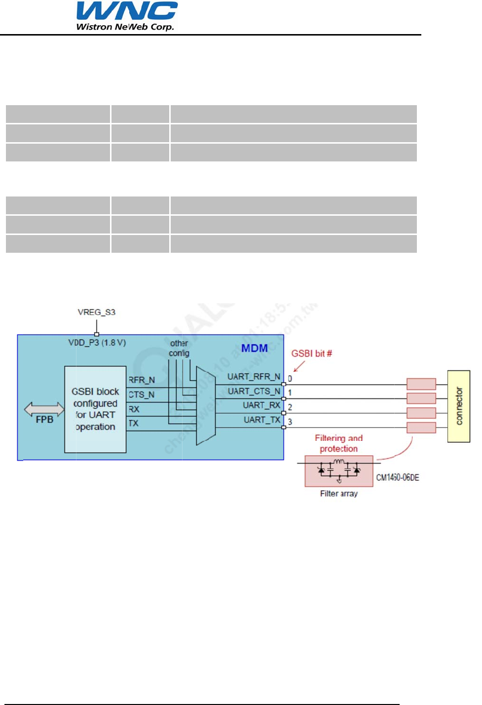
2.2.3 UART interface
The UART interface is provided on external pins of the module with the
following signals:
RX/TX
RFR/CTS
UART Speed
AT commands and DATA: up to 4 Mbit/s
Si
g
U
A
U
A
Si
g
U
A
U
A
2.2
.
2.2
.
A
U
Thi
s
sp
e
Software
2-pi
n
g
nal
A
RT2_TX
A
RT2_RX
2-pi
n
g
nal
A
RT3_TX
A
RT3_RX
.4
UA
R
.5
USB
U
SB link is
s
interfac
e
e
ed (12Mb
i
downloa
d
n
UART2 f
o
P
n
UART3 f
o
P
R
T CONNE
C
available
f
e
is compli
a
i
t/s) specif
i
: up to 1
M
o
r PLC
P
in N°
D
120
U
57
U
o
r Meter I
n
P
in N°
D
58
U
122
U
C
TION
Figure
4
f
or the AT
a
nt with th
e
i
cations.
User manu
a
M
bit/s
D
escription
U
ART Tran
U
ART Rec
e
n
terface
D
escription
U
ART Tran
U
ART Rec
e
4
: UART c
o
command
e
USB Hig
a
l of 3G SEP
(defined i
n
smit
e
ive
(defined i
n
smit
e
ive
o
nnection
s
and the
t
h Speed (
4
EVDO modu
n
Module’
s
n
Module’
s
t
race port.
4
80Mbit/s)
u
l
e
Page 15
s
direction
)
s
direction
)
)
and USB
)
)
Full
User manual of 3G SEP EVDO module
Page 16
If the USB feature is not used in the customers design, it is, however, strongly
recommended to leave this interface accessible through test points for debug
purposes.
Signal Pin N° Description
USB_DP 60 USB Data Positive
USB_DM 124 USB Data Negative
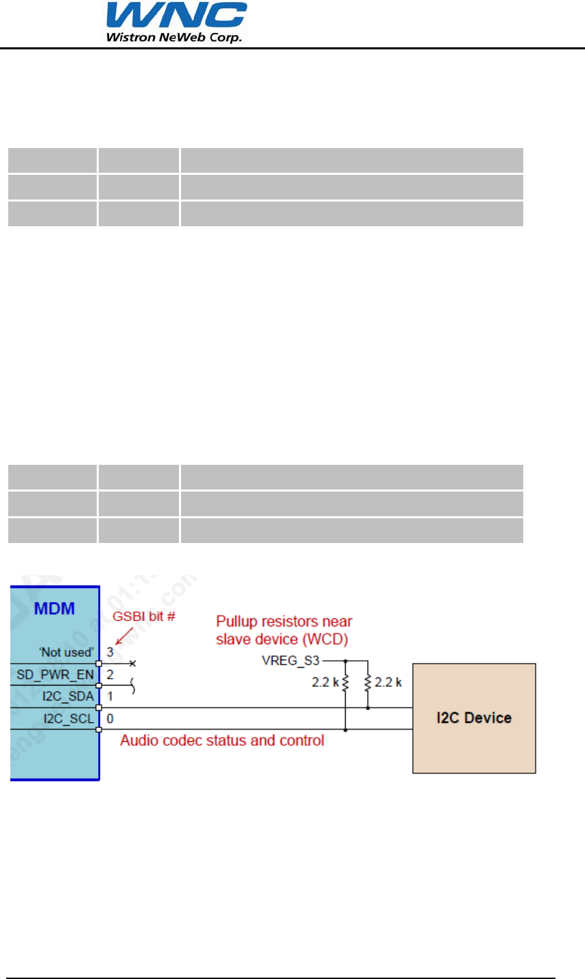
2.2.6 I2C Interface
I2C pins use GPIOs configured as open-drain outputs; the pull-up resistor is
provided by the slave. Two-wire bus for inter-IC communications supporting
any IC fabrication process.
High-speed mode (3.4 Mbps) is not supported.
10-bit addressing is not supported.
Fast mode plus (1 Mbps) is not supported.
Note: The MDM supports fast mode up to 400 kbps.
Signal Pin N° Description
I2C_SDA 53 I2C serial data
I2C_SCL 54 I2C serial clock
Figure 5: I2C connection
2.2.7 JTAG Interface
Test ports for debug
Si
g
S
M
J
T
J
T
J
T
J
T
J
T
J
T
J
T
2.2
.
Th
e
U
M
An
y
Si
g
S
P
S
P
S
P
S
P
g
nal
M
PS3
T
AG_RTC
K
T
AG_SRS
T
T
AG_TCK
T
AG_TDI
T
AG_TDO
T
AG_TMS
T
AG_TRS
T
.8
Seri
a
e
SPI allo
w
M
C-3GSEP
y
of the fi
v
g
nal
P
I_MOSI
P
I_MISO
P
I_CS_N
P
I_CLK
P
K
T
_N
T
_N
a
l periphe
r
w
s synchr
o
and a p
e
v
e GSBI p
P
P
in N°
D
29 J
T
30 J
T
96 J
T
93 J
T
94 J
T
31 J
T
95 J
T
32 J
T
al Interfac
e
o
nous seri
a
e
ripheral,
w
orts can
b
P
in N°
D
66 4
-
65 4
-
2 4
-
4 4
-
User manu
a
D
escription
T
AG VDD
T
AG retur
n
T
AG rese
t
T
AG cloc
k
T
AG data
T
AG data
T
AG mod
e
T
AG rese
t
e
a
l comm
u
w
ith the
M
b
e config
u
D
escription
-pin SPI
m
-pin SPI
m
-pin SPI c
h
-pin SPI cl
a
l of 3G SEP
(defined i
n
n
clock
for debug
k
input
input
output
e
select in
p
u
nication
M
DM devi
u
red as a
(defined i
n
m
aster out/
s
m
aster in/sl
h
ip select
ock
EVDO modu
n
Module’
s
p
ut
b
etween
ce as the
n SPI mas
n
Module’
s
s
lave in
a
ve out
u
l
e
Page 17
s
direction
)
the
e
master
o
ter.
s
direction
)
)
o
nly.
)
User manual of 3G SEP EVDO module
Page 18
2.2.9 Secure digital controller(sdc) ports
The MDM IC provides up to two SD interfaces, which provide the
following features or functions:
Up to 25 MB/s data rate
1.8 V / 2.95 V dual-voltage operation on SDC1;
Interface with SD/MMC memory cards up to 2 TB
10k pullup resistor on command pin; placeholder pullups are
recommended on the data lines also.
SDC1 for HPGP/PLC
Signal Pin N° Description
SDC1_CMD 48 Secure digital controller 1 command
SDC1_CLK 46 Secure digital controller 1 clock
SDC1_DATA0 47 Secure digital controller 1 data bit 0
SDC1_DATA1 112 Secure digital controller 1 data bit 1
SDC1_DATA2 111 Secure digital controller 1 data bit 2
SDC1_DATA3 110 Secure digital controller 1 data bit 3
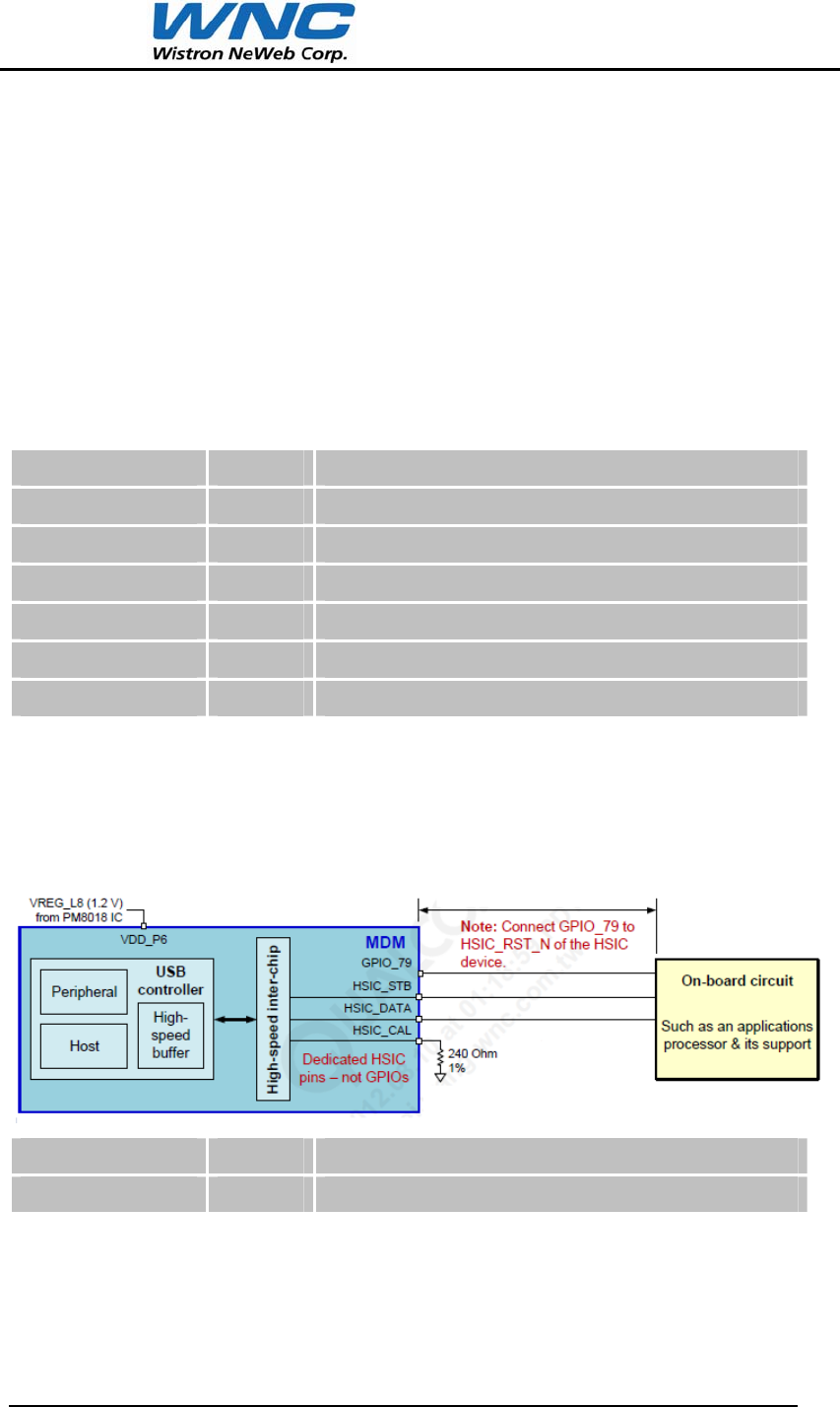
2.3 HIGH-SPEED INTER-CHIP (HSIC) INTERFACE
Eliminates the analog transceiver from a USB interface for lower voltage
operation and reduced power dissipation.
HSIC_DATA 69 HSIC data
HSIC_STB 72 HSIC strobe
2.4 GENERAL PURPOSE I/O
There are GPIO that can be customized easily from the customer’s application
User manual of 3G SEP EVDO module
Page 19
through appropriate AT commands and they can be configured as input or
output:
2.5 RESET
One reset input pin is available to reset the module in case of undesirable
behavior and internal pull up 1.8V with 40K ohm.
Signal Pin N° Description
PERST_N 97 Low level active input signal to reset the module
2.6 ADC
ADC input pin is available to measure an external analog voltage through
dedicated AT commands.
Signal Pin N° Description
POWER_DETECT1 34 Analog to digital converter input
POWER_DETECT2 99 Analog to digital converter input
XO_THERM 35 Analog to digital converter input
POWER OUTPUT
This Voltage pin is the 3V power supply for the peripheral.
Signal Pin N° Description
LDO4 39 3V Power supply
2.7 POWER SUPPLY & GND
3G SEP power supply & Ground pins. High input voltage range: 3.4 V to 4.2 V.

User manual of 3G SEP EVDO module
Page 20
Signal Pin N° Description
VPH_PWR 9,10,
37,38,102,103
Pin9/10 (for RF power)
Pin37/38/102/103 (for Baseband power)
GND 5,8,11,12,14,15,20,22,2
5,28,33,36,40,45,51,55,
61,69,72-157
Ground pins
2.8 POWER MANAGEMENT
2.9 SLEEP MODES
There are two kinds of sleep modes, the “off mode” and “stand-by” mode as
described below:
2.9.1 Off mode
When the module is in the off mode it cannot receive any calls or receive any
AT commands but can be awakened by using PWON signal.
2.9.2 Stand-by Mode Management
There are three stand-by mode management controls:
AT+KSLEEP=0
In this mode the sleep state is controlled by the host DTR and by the
firmware:
- DTR = 1 - The module never enters into the sleep mode
- DTR = 0 - The module enters the sleep mode when it is ready
and cannot be awakened with an AT command. To wake up the
module the user must toggle DTR to 1.
Remarks: Even in this mode it is possible to use DTR signals to go from
the data mode to the command mode. However, in this case, DTR has
to be toggled from 1 to 0 then from 0 to 1.
AT+KSLEEP=1
In this mode the sleep mode state is only controlled by the firmware.
The module enters the sleep mode when it is ready. The module may be

User manual of 3G SEP EVDO module
Page 21
awakened with any character received on the UART. However, to be
sure to awaken the module, the “0x00” character must be sent.
The main interest of the AT+KSLEEP=0 mode is to be able to forbid the sleep
mode from using the DTR signal.
AT+KSLEEP=2
In this mode the sleep state is never authorized in any DTR state.
Detailed descriptions of these modes are given in.
2.9.3 Power consumption
The power supply input of ranges from 3.4V to 4.2V and 4V is nominal.
All measurements in the communication mode are done at the maximum RF
power transmission (PCL max).
-30°C 25°C +85°C
Typ. Typ. Max Typ.
Off mode 50 µA 100 µA
Stand-by mode – connected to the
network (cell power -55dBm/1.23MHz) 150mA 150mA 200mA 150mA
C2K 1X
TX: Maximun power
All band 700mA 700mA 780mA 700mA
EVDO data mode
TX: Maximun power
All band 680mA 680mA 750mA 680mA

User manual of 3G SEP EVDO module
Page 22
2.10 RTC FUNCUTION
One reset input pin is available to reset the module in case of undesirable
behavior and internal pull up 1.8V with 40K ohm.
Signal Pin N° Description
PERST_N 97 Low level active input signal to reset the module
User manual of 3G SEP EVDO module
Page 23
3. PINOUT
3.1 I/O CONNECTOR PIN ASSIGNMENTS
Pin number Category 3G SEP pin
definitions
MDM9615 pad
name
PM8018 pad
name Pad type
9
VPH_PWR
(4V / 3A)
RF_VPH_PWR1 104: VDD_S1 4V/3A
10 RF_VPH_PWR2 4V/3A
37 BB_VPH_PWR1 4V/3A
38 BB_VPH_PWR2 4V/3A
102 BB_VPH_PWR3 4V/3A
103 BB_VPH_PWR4 4V/3A
39
3V Power
for
peripheral
(3.075V /
300mA)
LDO4 84: VREG_L4 3.075V /
0.3A
48
SDC1 for
HPGP/PLC
(SDC1=2.9
5V)
SDC1_CMD W21: SDC1_CMD B
46 SDC1_CLK W23: SDC1_CLK DO
47 SDC1_DATA0 W22:
SDC1_DATA_0 B
112 SDC1_DATA1 V21:
SDC1_DATA_1 B
111 SDC1_DATA2 V22:
SDC1_DATA_2 B
110 SDC1_DATA3 V23:
SDC1_DATA_3 B
108
SDC2 for
Wi-fi
(1.8V)
SDC2_CMD AA21: GPIO_29 B-PD
42 SDC2_CLK AC22: GPIO_30 BH-PD,
/INT
107 SDC2_DATA0 AB21: GPIO_25 B-PD
43 SDC2_DATA1 AB22: GPIO_26 BH-PD,
/INT
User manual of 3G SEP EVDO module
Page 24
44 SDC2_DATA2 AA22: GPIO_27 BH-PD,
/INT
106 SDC2_DATA3 AC21: GPIO_28 BH-PD,
/INT
105 WLAN_PWR_DO
WN Y3: GPIO_72 B-PD
41 SDC2_GPIO W3: GPIO_73 B-PD
83
Power
Control
(1.8V)
CAPGOOD M5: GPIO_59 BH-PD,
/INT
82 RAD_DC_ON R2: GPIO_60 B-PD
81 PLC_DC_ON N1: GPIO_61 B-PD
18 EN_CHG AA1: GPIO_32 B-PD
19 POWER_FAIL V5: GPIO_45 BH-PD,
/INT
62
4-pin
UART1 for
EM357
Zigbee
(1.8V)
UART1_TX B7: GPIO_11 BH-PD,
/INT
63 UART1_RX A7: GPIO_10 BH-PD,
/INT
64 UART1_CTS A6: GPIO_9 B-PU
126 UART1_RFR B6: GPIO_8 B-PD
128 ZB_RESET J5: GPIO_67 B-PD
1 ZB_PA5 M2: GPIO_68 B-PD,
/INT
127 ZB_PC6 H5: GPIO_69 BH-PD,
/INT
120 2-pin
UART2 for
PLC
(1.8V)
UART2_TX A12: GPIO_15 BH-PD,
/INT
57 UART2_RX A10: GPIO_14 BH-PD,
/INT
56 PLC_RESET E12: GPIO_17 BH-PU,
/INT
121 PLC_EN A9: GPIO_16 B-PU
58 2-pin
UART3 for
Meter
Interface
UART3_TX B12: GPIO_19 BH-PU,
/INT
122 UART3_RX C11: GPIO_18 BH-PD,
/INT
59 8215_EPF M1: GPIO_62 B-PD
User manual of 3G SEP EVDO module
Page 25
(1.8V)
53
I2C for
Accelerome
ter or LCM
(1.8 V)
I2C_SDA B9: GPIO_13 B-PD
54 I2C_SCL C8: GPIO_12 B-PU
52 I2C_RESET M3: GPIO_82 BH-PD,
/INT
117 I2C_INT J3:GPIO_84 BH-PD,
/INT
118 TILT_INT J1: GPIO_80 BH-PD,
/INT
55
USB for
Debug Port
USB_HS_ID F9: USB_HS_ID AI, AO
25 5V_BOOST_EN 60: GPIO_04
60 USB_HS_DP C9: USB_HS_DP AI, AO
124 USB_HS_DM E9: USB_HS_DM AI, AO
29
JTAG for
Debug Port
(JTAG
Power:
1.8V)
SMPS3 42: VSW_S3 1.8V /
1.5A
30 JTAG_RTCK AC4: RTCK DO
96 JTAG_SRST_N W6: SRST_N DISH-PU
93 JTAG_TCK AC3: TCK DIS-PU
94 JTAG_TDI AC5: TDI DIS-PU
31 JTAG_TDO AB5: TDO DO-Z
95 JTAG_TMS AA5: TMS DIS-PU
32 JTAG_TRST_N AA6: TRST_N DISH-PD
66
SPI for
Water/GAS
AMR
(1.8V)
SPI_MOSI E3: GPIO_7 BH-PU,
/INT
65 SPI_MISO D2: GPIO_6 BH-PD,
/INT
2 SPI_CS_N E2: GPIO_5 BH-PD,
/INT
4 SPI_CLK G5: GPIO_4 BH-PD,
/INT
3 ISM_IRQ G1: GPIO_78 BH-PD ,/I
NT
68 ISM_RESET_N N3: GPIO_64 B-PD
User manual of 3G SEP EVDO module
Page 26
67 ISM_CC1190_HG
M L3: GPIO_65 B-PD
27 UIM for
SIM Card
Socket
(1.8V or
2.85V )
UIM1_DATA E1: GPIO_3 BH-PU,
/INT
90 UIM1_CLK C3: GPIO_2 BH-PD,
/INT
26 UIM1_RESET F3: GPIO_1 BH-PD,
/INT
91 LDO6 17: VREG_L6 1.8 or
2.85V /
0.15A
97 Power reset
(1.8V) PERST_N 16: RESIN_N 1.8V
17 Heater
(1.8V) HTR_ON 50:GPIO_03
34 ADC_IN
Scaling 1
(0.1 to
1.7V)
Scaling 1/3
(0.3 to
VPH_PWR)
POWER_DETECT
1 85: MPP_01 AO-Z
99 POWER_DETECT
2 67: MPP_02 AO-Z
35 XO_THERM 73: MPP_05 AO-Z
24
LEDs
(1.8V)
LED0_GREEN W5:GPIO_35 B-PD
88 LED0_RED W2:GPIO_38 B-PD
87 LED1_GREEN W1: GPIO_39 B-PD
23 LED1_RED 60: GPIO_04
7
Other
GPIOs
(1.8V)
ANT_SEL P2: GPIO_63 B-PD
71 MAG_SW K3: GPIO_77 BH-PD ,/I
NT
6 LIMIT_SW AB1:GPIO_40 BH-PD,
/INT
70 GPS_LNA_EN K5: GPIO_66 B-PD
114 I2S/PCM
Analog
Audio for
I2S_MCLK C13: GPIO_24 BH-PD,
/INT
50 I2S/PCM_TX A13: GPIO_23 BH-PD,
/INT
User manual of 3G SEP EVDO module
Page 27
115 Alarm
(1.8V) I2S/PCM_RX B13: GPIO_22 BH-PU,
/INT
49 I2S_WS/PCM_SY
NC E13: GPIO_21 B-PD
113 I2S/PCM_CLK C12: GPIO_20 BH-PD,
/INT
100 VCOIN for
RTC VCOIN 57: VCOIN
33 for SW
download DOWNLOAD 49: GPIO_06
75
HSIC
HSIC_READY G2: GPIO_79 BH-PD,
/INT
69 HSIC_DATA C2: HSIC_DATA
72 HSIC_STB C1: HSIC_STB
5 GND
8 GND
11 GND
12 GND
14 GND
15 GND
20 GND
22 GND
28 GND
36 GND
40 GND
45 GND
51 GND
61 GND
73 GND
74 GND
76 GND

User manual of 3G SEP EVDO module
Page 28
77 GND
78 GND
79 GND
80 GND
84 GND
85 GND
86 GND
89 GND
92 GND
98 GND
101 GND
104 GND
109 GND
116 GND
119 GND
123 GND
125 GND
129 GND
130 GND
131 GND
132 GND
133 GND
134 GND
135 GND
136 GND
137 GND
138 GND

User manual of 3G SEP EVDO module
Page 29
139 GND
140 GND
141 GND
142 GND
143 GND
144 GND
145 GND
146 GND
147 GND
148 GND
149 GND
150 GND
151 GND
152 GND
153 GND
154 GND
155 GND
156 GND
157 GND
13
RF
RF_MAIN
16 RF_DRX
21 RF_GPS
User manual of 3G SEP EVDO module
Page 30
4. ELECTRICAL SPECIFICATIONS
Five system operating states are defined:
NO SUPPLY: No power voltage is present.
OFF: Main power voltage is present.
ACTIVE: Main power voltage is present Internal power supplies are on.
SLEEP: Main power voltage is present Internal power supplies are in the
low power mode.
If not specified, all electrical values are given for the active state at
VPH_PWR=4.0V and an operating temperature of 25°C.
4.1 VPH PWR
The module is supplied through the VPH_PWR with the following
characteristics:
Parameter Name Min. Typ. Max.
VPH_PWR maximum
voltage (V)
VPH_PWR (*) - - 4.2
VPH_PWR minimum voltage
(V)
VPH_PWR (*) 3.4 - -
VPH_PWR drop voltage
(mV)
DeltaVbat (*) - - 300 (**)
Transient voltage (V) TBD - -
Noise level
(Vrms)@100KHz-1MHz
- - 50mV
* See Application Notes for more details.
** This value depends on the power supply serial resistor (plus contact and
track serial resistors)
4.2 VBACKUP
Parameter Min. Typ. Max
.
Remarks
Voltage level(V) 1.2 3 3.25
User manual of 3G SEP EVDO module
Page 31
4.3 VSIM
Parameter Min. Typ. Max
.
Remarks
Output Voltage(V) 2.7 3 3.15 The appropriate output voltage is
auto detected and selected by
software.
1.65 1.80 1.95
Output Current (mA) - - 150
Line Regulation (mV/V) - - 50 IOUT = MAX
Power-up Setting Time (us)
from power down
- 10 -
4.4 DIGITAL INTERFACE
The digital interface has the following characteristics, which includes UART,
PCM/I2S,I2C, GPIOs, SPI and SDIO.
Parameter Min. Typ. Max. Remarks
Input Current-High(µA) -10 - 10
Input Current-Low(µA) -10 - 10
DC Output
Current-High(mA) (1)
- - 10 Pin driving a "1" with output set at "0"
DC Output
Current-Low(mA) (1)
-10 - - Pin driving a "0" with output set at "1"
Input Voltage-High(V) 1.7 2.0
Input Voltage-Low(V) -0.3 - 0.3
Output Voltage-High(V) 1.7 - 2.0
Output Voltage-Low(V) 0 - 0.3
(1) The maximum current for one GPIO is 10mA.
4.5 RESET
The RESET signal has the following characteristics:
Parameter Min. Typ. Max
.
User manual of 3G SEP EVDO module
Page 32
Input Voltage-Low (V) -0.3 0 0.3
Input Voltage-High(V) 1.2 1.8 2.1
Power up Period (ms) from RESET falling edge 20 - -
4.6 SIM
Signal VL (V) VH (V)
Min. Max. Min. Max.
SIM_RST Fully compliant to the GSM11.11 and ISO/IEC 7816-3 standards
SIM_CLK
SIM_DATA
I2C INTERFACE
I2C HAS THE FOLLOWING CHARACTERISTICS:
Applicable standard Feature exceptions MDM
variations
I2C Specification, version 2.1,
January 2000 (Phillips Semiconductor
document number 9398 393 40011)
.High-speed mode (3.4 Mbps) is not supported.
.10-bit addressing is not supported.
.Fast mode plus (1 Mbps) is not supported.
Note: The MDM supports fast mode up to 400 kbps
None
4.7 USB
USB signals have the following characteristics:
Signal VL (V) VH (V)
Min Max Min Max
USB_HS_DP 0 0.3 - 5.25
USB_HS_DM 0 0.3 - 5.25
USB_HS_VBUS 0 0.3 2.0 5.25
4.8 ADC
The ADC has the following characteristics.
Affiliate PMIC Typical input (V) Scaling Typical output (V)
User manual of 3G SEP EVDO module
Page 33
pins/function
MPP_XX (selectable) 0.1 to 1.7 1 0.1 to 1.7
MPP_XX (selectable) 0.3 to VPH_PWR 1/3 0.1 to 1.7
4.9 UART
TX, RX, CTS, and RFR have the following characteristics:
Signal VL (V) VH (V)
Min Max Min Max
UART_TX -0.3 0.4 1.5 2.1
UART_RX -0.3 0.4 1.5 2.1
UART_RFR -0.3 0.4 1.5 2.1
UART_CTS -0.3 0.4 1.5 2.1
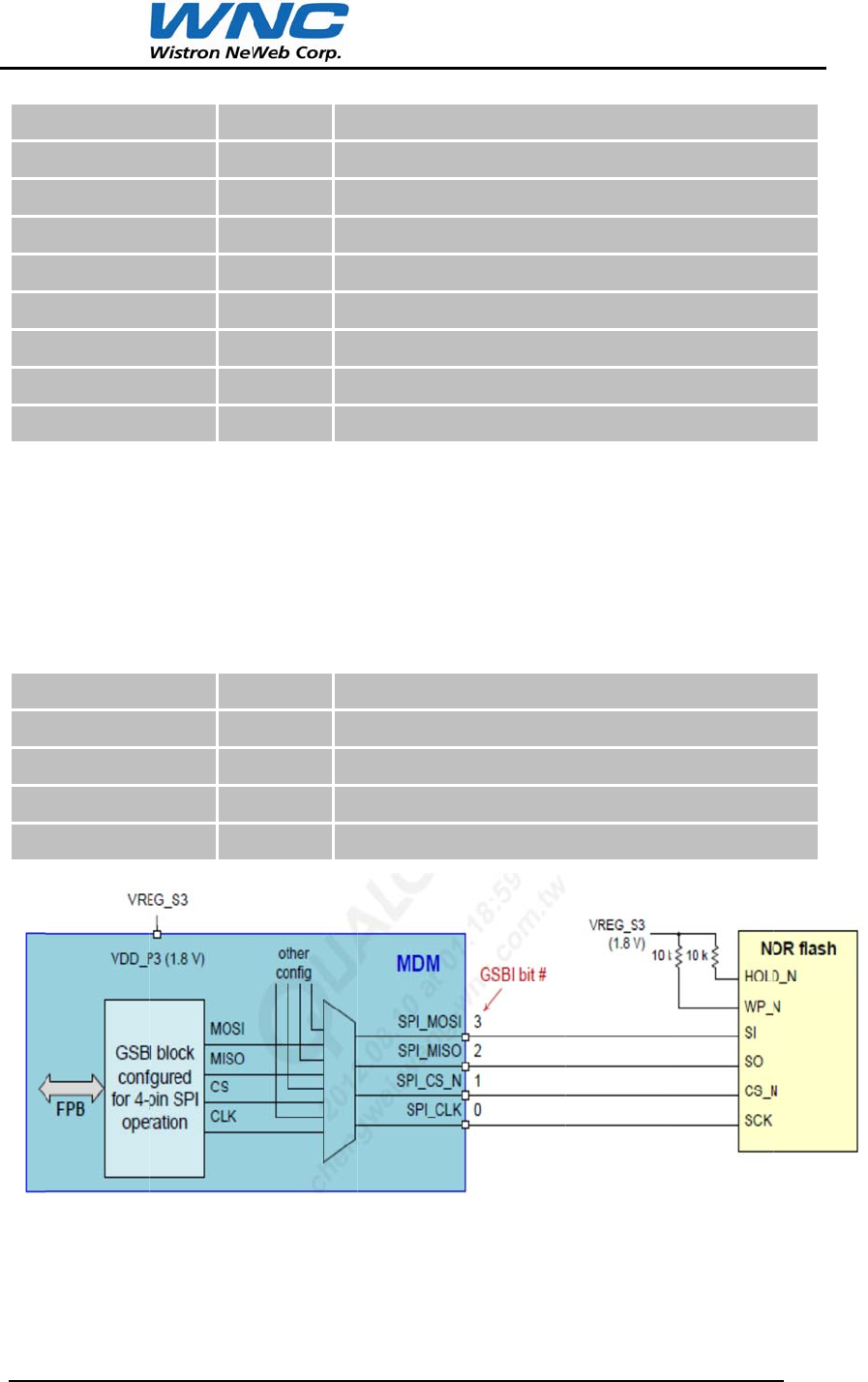
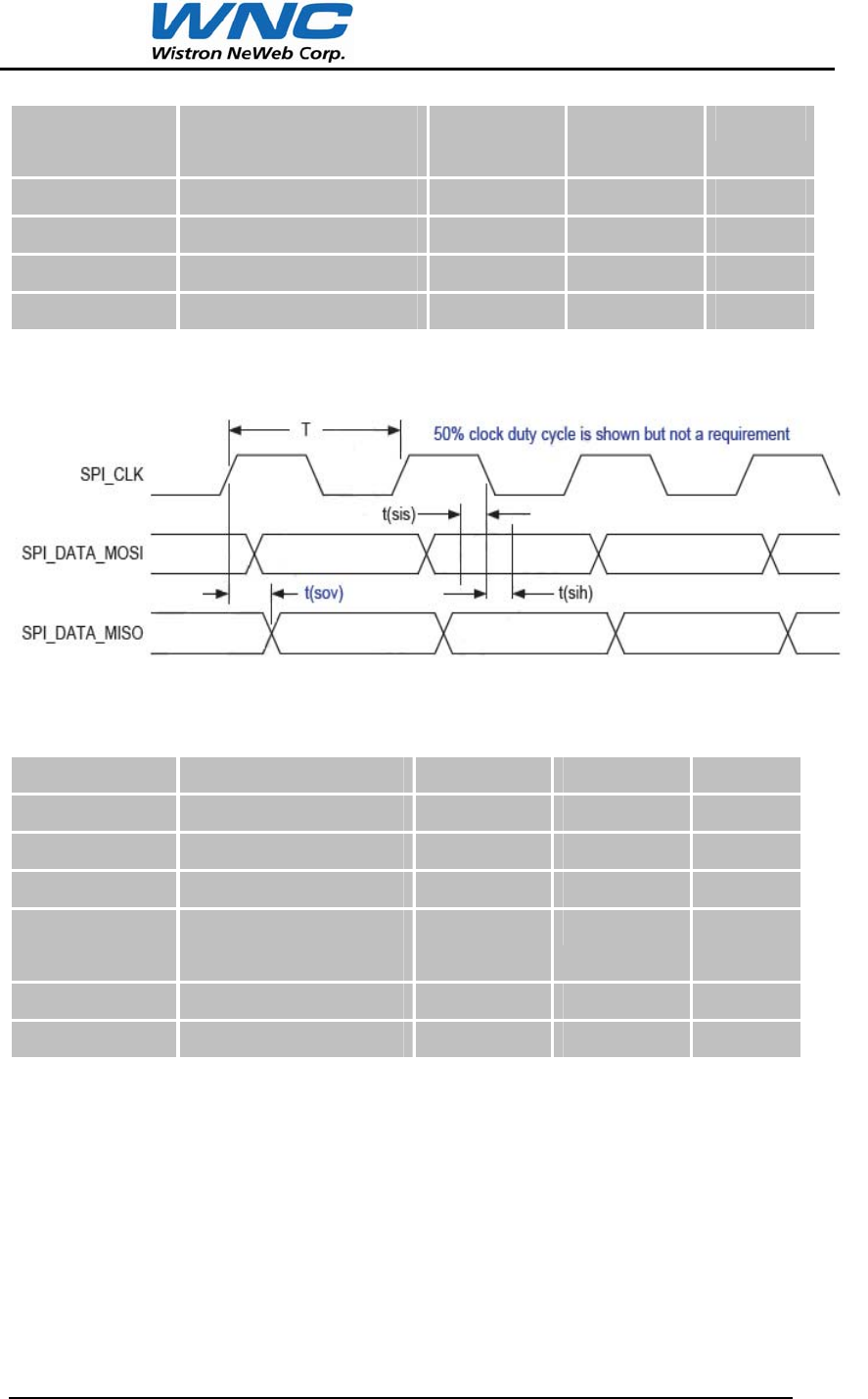
4.10 SPI
The SPI allows duplex (or half-duplex) and synchronous serial communication
between a master and a slave.
3G SEP can be configured as an SPI master or slave mode.
Figure 8: SPI in the master mode
Parameter Comments Minimum Maximum Unit
1/T SPI clock frequency - 26 MHz
T SPI clock period 38 - ns
t(ch) Clock high 0.45xT 0.55xT ns
t(cl) Clock low 0.45xT 0.55xT ns
User manual of 3G SEP EVDO module
Page 34
t(mov) Master output data
uncertainty
-5 5 ns
t(mis) Master input setup 0 3 ns
t(moh) Master output hold 0 3 ns
t(tse) Tri-state enable -5 5 ns
t(tsd) Tri-state disable -5 5 ns
Figure 9: SPI in the slave mode
Parameter Comments Minimum Maximum Unit
1/T SPI clock frequency - 26 MHz
t(ch) Clock high 0.45xT 0.55xT ns
t(cl) Clock low 0.45xT 0.55xT ns
t(sov) Slave output data
uncertainty
0 15.8 ns
t(sis) Slave input setup 1.5 - ns
t(sih) Slave input hold 1.5 - ns
4.11 SDIO
Only supports the master mode.
User manual of 3G SEP EVDO module
Page 35
Figure 10: SDIO timing
Single data rate (SDR) 1
Parameter Comments Minimum Maximum Unit
t(chrd) Command hold 2.5 ns
t(csurd) Command setup 6.0 ns
t(dhrd) data hold 2.5 ns
t(dsurd) Data setup 5.0 ns
t(pddwr) Propagation delay on data
write
-7 3 ns
t(pdcwr) Propagation delay on
command write
-7 3 ns
Double data rate (DDR) 2
Parameter Comments Minimum Maximum Unit
t(chrd) Command hold 1.5 ns
t(csurd) Command setup 12.3 ns
t(dhrd) data hold 1.5 ns
t(dsurd) Data setup 4.7 ns
t(pddwr) Propagation delay on data
write
0.8 8.7 ns
User manual of 3G SEP EVDO module
Page 36
t(pdcwr) Propagation delay on
command write
-10.9 5.7 ns
4.12 HIGH-SPEED INTER-CHIP (HSIC) INTERFACE
High-Speed Inter-Chip USB Electrical Specification, version 1.0 (a supplement
to the USB 2.0 specification,
4.13 DIGITAL AUDIO
THE AUDIO OUTPUTS CONTAIN THE FOLLOWING CHARACTERISTICS:
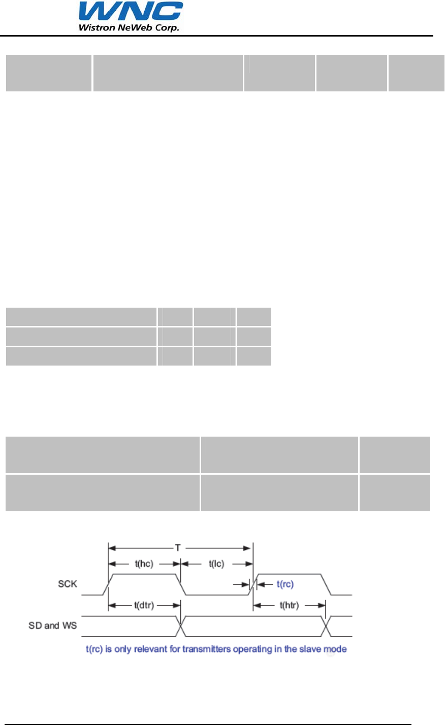
4.14.1 I2S Interface
The I2S interface signaling and timing is identical, regardless of whether I2S is selected as the
mode of operation for the primary and/or secondary audio interface.
Applicable standard Feature exceptions MDM
variations
Phillips I2S Bus Specifications, revised
June 5, 1996
No external controller support None
Figure 11: I2S transmitter timing diagram
Parameter Min Typ Max
Maximum input range 1.6 1.8V 2.1
Maximum output range 1.6 1.8V 2.1
User manual of 3G SEP EVDO module
Page 37
Parameter Condition Min Typ Max Unit
T Clock period I2S requirement: min T = 293 293 326 359 ns
t(hc) Clock high I2S requirement: min > 0.35T 120 ns
t(lc) Clock low I2S requirement: min > 0.35T 120 ns
t(dtr) Delay I2S requirement: max < 0.8T 250 ns
t(htr) Hold time I2S requirement: min > 0 100 ns
Figure 12: I2S receiver timing diagram
Parameter Condition Min Typ Max Unit
T Clock period I2S requirement: min T = 293 293 326 359 ns
t(hc) Clock high I2S requirement: min < 0.35T = 103 100 - - ns
t(lc) Clock low I2S requirement: min < 0.35T = 103 100 - - ns
t(sr) Setup time I2S requirement: min < 0.2T = 59 40 - - ns
t(htr) Hold time I2S requirement: min < 0 0 - - ns
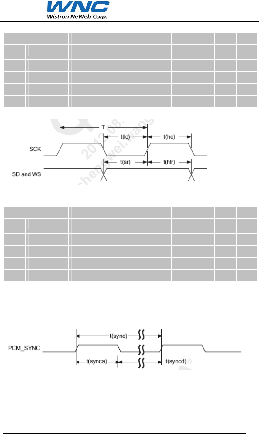
4.14.2 PCM Interface
4.14.2.1 Primary (short sync) PCM interface (2048 kHz clock)
Figure 13: PCM_SYNC timing
User manual of 3G SEP EVDO module
Page 38
Figure 14: PCM_CODEC to MDM timing
Figure 15: MDM to PCM_CODEC timing
Parameter Condition Mi
n
Typ Max Unit
t(sync) PCM_SYNC cycle time - 125 - us
t(synca) PCM_SYNC asserted time - 488 - ns
t(syncd) PCM_SYNC de-asserted time - 124.5 - us
t(clk) PCM_CLK cycle time - 488 - ns
t(clkh) PCM_CLK high time - 244 - ns
t(clkl) PCM_CLK low time - 244 - ns
t(sync_o
ffset)
PCM_SYNC offset time to
PCM_CLK falling
- 122 - ns
t(sudin) PCM_DIN setup time to
PCM_CLK falling 60 - - ns
t(hdin) PCM_DIN hold time after
PCM_CLK falling
60 - - ns
User manual of 3G SEP EVDO module
Page 39
t(pdout) Delay from PCM_CLK rising to
PCM_DOUT valid
- - 60 ns
t(zdout) Delay from PCM_CLK falling to
PCM_DOUT HIGH-Z
- - 60 ns
4.14.2.2 Auxiliary (long sync) PCM interface (128 kHz clock)
Figure 16: AUX_PCM_SYNC timing
Figure 17: AUX_PCM_CODEC to MDM timing
Figure 18: MDM to AUX_PCM_CODEC timing
Parameter Condition Min Typ Max Unit
t(auxsync) AUX_PCM_SYNC cycle time - 125 - us
t(auxsynca) AUX_PCM_SYNC asserted time 62.4 62.5 - us
User manual of 3G SEP EVDO module
Page 40
t(auxsyncd) AUX_PCM_SYNC de-asserted time 62.4 62.5 - us
t(auxclk) AUX_PCM_CLK cycle time - 7.8 - us
t(auxclkh) AUX_PCM_CLK high time 3.8 3.9 - us
t(auxclkl) AUX_PCM_CLK low time 3.8 3.9 - us
t(suauxsync) AUX_PCM_SYNC setup time to
AUX_PCM_CLK rising
1.95 - - ns
t(hauxsync) PCM_SYNC hold time after
AUX_PCM_CLK rising
1.95 - - ns
t(suauxdin) AUX_PCM_DIN setup time to
AUX_PCM_CLK falling
70 - - ns
t(hauxdin) AUX_PCM_DIN hold time after
AUX_PCM_CLK falling
20 - - ns
t(pauxdout) Delay from AUX_PCM_CLK to
AUX_PCM_DOUT valid
- - 50 ns
4.14 RF SIGNAL
4.14.1 Load mismatch
The module accepts a VSWR < 20:1 (all phase angles) without damage or
permanent degradation.
The module accepts a VSWR < 12:1 (all phase angles) without any spurious
emission > - 30 dBm.
4.14.2 Input VSWR
The typical input VSWR is 1.5:1 (max = 1.5:1).
4.14.3 Antenna matching network
A matching network in the UMC-3GSEP module is optimized for a 50 ohm
work load.
To obtain the best performance in an application, an additional matching circuit
and adjustment for actual antenna is required. A π-type matching network is
recommended in the UMC-3GSEP Application Note.
User manual of 3G SEP EVDO module
Page 41
5. ENVIRONMENTAL SPECIFICATIONS
Parameter
Min. Max.
Ambient temperature
Normal range
-20°C +70°C
Ambient temperature
Extended range
-30°C +85°C
Storage temperature -40°C +105°C
Long damp heat
Operating conditions
Tested at +60°C, 95% RH during a 504 hour
period
Short damp heat
Storage and transportation
conditions
Tested at +40°C, 95% RH during a 96 hour
period
5.1 NORMAL TEMPERATURE RANGE
ETSI performances are guaranteed by WNC in the range of -20°C to +70°C.
5.1.1 Conduct RX Sensitivity at the normal temperature range
Enhanced sensitivity performance at 25°C is guaranteed as follow:
Frequency bands MAX 3GPP2 C.S0033
min. standard
BC0 CDMA 1x0.5% FER -107dBm -104dBm
EVDO rev A0.5% PER -107dBm -105.5dBm
BC1 CDMA 1x0.5% FER -107dBm -104dBm
EVDO rev A0.5% PER -107dBm -105.5dBm
User manual of 3G SEP EVDO module
Page 42
5.1.2 Typical transmission values at normal temperature range
Typical transmission values is as below
Frequency band Typ.
3GPP2 C.S0033
min. standard
BC0 class III 24dBm +/- 1dB ERP 0.2 W
BC1 class II 24dBm +/- 1dB EIRP 0.2 W
5.2 EXTENDED TEMPERATURE RANGE
5.2.1 Typical Cellular sensitivity at extended temperature range
Frequency band BC0 3GPP2 C.S0033
min. standard Temperature (°C) -30 +85
Typical sensitivity (dBm) (TBD) (TBD) < -105.5dBm
Frequency band BC1 3GPP2 C.S0033
min. standard Temperature (°C) -30 +85
Typical sensitivity (dBm) (TBD) (TBD) < -105.5dBm

User manual of 3G SEP EVDO module
Page 43
6. FCC WARNING STATEMENT
6.1 GENERAL
This manual is limited to OEM/Integrators installation only.
OEM integrators are responsible for ensuring that the end-user has no manual
instructions to remove or install module.
6.2 END PRODUCT LABELING (FCC)
When the module is installed in the host device, the FCC ID label must be visible
through a window on the final device or it must be visible when an access panel, door
or cover is easily re-moved. If not, a second label must be placed on the outside of the
final device that contains the following text: “Contains FCC ID: NKR96E1”.
The grantee's FCC ID can be used only when all FCC compliance requirements are
met.
6.3 REQUIRED FCC COMPLIANCE STATEMENT FOR HOST
INTEGRATION
To integrate this module into the host, the host manufacturer is responsible for the
applicable FCC rules, including the limits for a Class B digital device, pursuant to
Part 15 of the FCC Rules.
In the user manual of the host device, the following statements are required to be
included.
This device complies with part 15 of the FCC Rules. Operation is subject to the
following two conditions: (1) This device may not cause harmful interference,
and (2) this device must accept any interference received, including interference
that may cause undesired operation.
This device has been tested and found to comply with the limits for a Class B
digital device, pursuant to Part 15 of the FCC Rules. These limits are designed to
provide reasonable protection against harmful interference in a residential
installation. This equipment generates, uses and can radiated radio frequency
energy and, if not installed and used in accordance with the instructions, may

User manual of 3G SEP EVDO module
Page 44
cause harmful interference to radio communications. However, there is no
guarantee that interference will not occur in a particular installation If this
equipment does cause harmful interference to radio or television reception, which
can be determined by turning the equipment off and on, the user is encouraged to
try to correct the interference by one or more of the following measures:
–Reorient or relocate the receiving antenna.
–Increase the separation between the equipment and receiver.
–Connect the equipment into an outlet on a circuit different from that to which
the receiver is connected.
–Consult the dealer or an experienced radio/TV technician for help.
Changes or modifications not expressly approved by the party responsible for
compliance could void the user‘s authority to operate the equipment.
6.4 FCC MODULE INTEGRATION RESTRICTION:
This module has been certified by FCC as single module approval with the following
restrictions:
1. The monopole antenna with 2.0 dBi gain was verified in the conformity testing.
Radiated transmit power must be equal to or lower than that specified in the FCC
Grant of Equipment Authorization for FCC ID: NKR96E1. A separate approval is
required for all other operating configurations.
2. This module is limited to be installed in mobile or fixed application. To assure RF
Exposure compliance, the antenna used with this module should be installed and
operated with minimum distance 20 cm from all persons and must not transmit
simultaneously with any other antenna or transmitter, except in accordance with
FCC multi transmitter product procedure.
3. If any other simultaneous transmission radio is installed in the host platform
together with this module, or above restrictions cannot be kept, a separate RF
exposure assessment and FCC equipment authorization is required.