Wistron NeWeb IMS2 LTE Cat-M1 Module User Manual
Wistron NeWeb Corporation LTE Cat-M1 Module
User Manual
□ Normal □ Internal Use Confidential □ Restricted Confidential 1 / 26
IMS2 module user manual
Project Name: IMS2
Author: Wistron NeWeb Corporation
Revision: 1.1
Revision Date: 2017/09/13
Product datasheet
□ Normal □ Internal Use Confidential □ Restricted Confidential 2 / 29
Contact Information
Technical Support Website
https://SupportIoT.wnc.com.tw
Company Website
www.wnc.com.tw
Revision History
Rev. #
Author
Summary of Changes
Date
1.0
WNC
First release
2017/07/14
1.1
WNC
Add FCC statement and manual information to
the end user in the user manual
2017/09/13

Product datasheet
□ Normal □ Internal Use Confidential □ Restricted Confidential 3 / 29
© Wistron NeWeb Corporation
THIS DOCUMENT AND THE INFORMATION CONTAINED HEREIN IS PROPRIETARY AND
IS THE EXCLUSIVE PROPERTY OF WNC AND SHALL NOT BE DISTRIBUTED,
REPRODUCED, OR DISCLOSED IN WHOLE OR IN PART WITHOUT PRIOR WRITTEN
PERMISSION FROM WNC.
LIMITATION OF LIABILITY
THIS DOCUMENT AND THE INFORMATION CONTAINED HEREIN IS PURELY FOR
DESIGN REFERENCE AND SUBJECT TO REVISION BY WNC AT ANY TIME. NOTHING IN
THIS DOCUMENT SHALL BE CONSTRUED AS GRANTING ANY WARRANTY OR RIGHT
TO USE THE MATERIAL CONTAINED HEREIN WITHOUT WNC’S PRIOR EXPRESS
WRITTEN CONSENT. WNC SHALL NOT BE LIABLE FOR ANY USE, APPLICATION OR
DEVELOPMENT DERIVED FROM THE MATERIAL WITHOUT SUCH PRIOR EXPRESS
WRITTEN CONSENT.
FCC Statement
Please notice that if the FCC identification number is not visible when the module is
installed inside another device, then the outside of the device into which the module
is installed must also display a label referring to the enclosed module. This exterior
label can use wording such as the following: “Contains FCC ID:NKRIMS2”. Any similar
wording that expresses the same meaning may be used.
Manual Information to the End User
The module is limited to OEM installation ONLY.
The OEM integrator is responsible for ensuring that the end-user has no manual
instruction to remove or install module.
The module is limited to installation in mobile application; a separate approval is
required for all other operating configurations, including portable configurations
with respect to Part 2.1093 and difference antenna configurations.
This equipment complies with FCC radiation exposure limits set forth for an
uncontrolled environment. This equipment should be installed and operated with a
minimum distance of 20cm between the radiator & your body. This transmitter must
not be co-located or operating in conjunction with any other antenna or transmitter.

Product datasheet
□ Normal □ Internal Use Confidential □ Restricted Confidential 4 / 29
Contents
Contact Information .......................................................................................................................... 2
Revision History ............................................................................................................................... 2
1 Product Features ...................................................................................................................... 6
1.1 Features Description ........................................................................................................... 6
2 Pin Definitions ......................................................................................................................... 8
2.1 LGA Module Pin Diagram .................................................................................................. 8
2.2 LGA Module Pin Definitions .............................................................................................. 8
3 Electrical Specifications ......................................................................................................... 12
3.1 Electrical Operating Conditions ........................................................................................ 12
3.1.1 Detailed Information .............................................................................................. 12
3.1.2 Power Tree ............................................................................................................. 12
3.2 Control Interfaces .............................................................................................................. 13
3.2.1 Power-on Signal (TBD) ......................................................................................... 13
3.2.2 Wake-up Interface (TBD) ...................................................................................... 13
3.2.3 Reset Signal ............................................................................................................ 14
3.3 UART Interface ................................................................................................................. 14
3.4 UIM Interface .................................................................................................................... 15
3.5 I/O Characteristics ............................................................................................................. 15
3.6 JTAG Interface .................................................................................................................. 17
3.7 Power Consumption .......................................................................................................... 17
3.8 RF Performance ................................................................................................................ 18
3.8.1 RF Pad Design ....................................................................................................... 18
3.8.2 RF Matching Guide ................................................................................................ 21
3.8.3 Interference and Sensitivity .................................................................................... 21
3.8.4 Band Support .......................................................................................................... 22
3.8.5 Bandwidth Support................................................................................................. 22
3.8.6 RF Transmission Specifications ............................................................................. 22
3.8.7 RF Receiver Specifications .................................................................................... 23
3.9 Temperature ...................................................................................................................... 23
3.10 LTE Power Saving Mode ................................................................................................ 23
3.11 Serial Number and IMEI ................................................................................................. 23
4 Mechanical Information ......................................................................................................... 25
4.1 Physical Dimensions ......................................................................................................... 25
4.2 Pin Dimensions ................................................................................................................. 25
4.3 Marking Information ......................................................................................................... 27
5 Packing Information............................................................................................................... 28
5.1 Packing Information .......................................................................................................... 28
5.2 Storage Conditions ............................................................................................................ 28
6 PCB Mounting Guidelines ..................................................................................................... 28
6.1 Mounting Considerations .................................................................................................. 28
7 Regulatory and Industry Approval ......................................................................................... 28
7.1 Certification Testing ......................................................................................................... 28

Product datasheet
□ Normal □ Internal Use Confidential □ Restricted Confidential 5 / 29
7.2 GP Compliance ................................................................................................................. 28
Initialisms ........................................................................................................................................ 29
□ Normal □ Internal Use Confidential □ Restricted Confidential 6 / 26
1 Product Features
1.1 Features Description
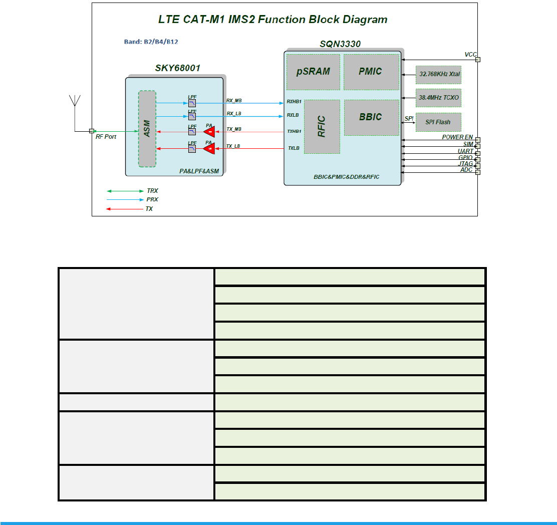
The WNC IMS2 module includes the Sequans SQN3330 Cat. M1 baseband, a
complete three LTE band (2/4/12) RF front-end, memory, and required circuitry to
fulfill 3GPP E-UTRA (Long Term Evolution - LTE, Release 13 specifications) and
AT&T Wireless LTE Cat. M1 UE specifications.
The architecture block diagram of the IMS2 is presented in Figure 1-1 below.
Figure 1-1. IMS2 block diagram
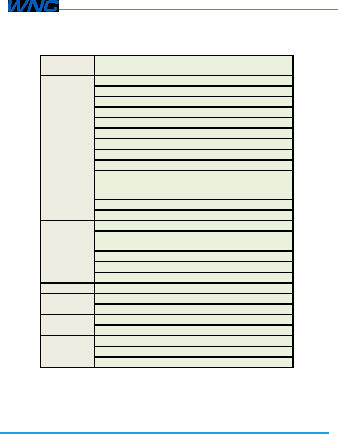
Table 1-1. General features of the IMS2
General interfaces
• JTAG
• USIM
• GPIO
• UART
Supported frequency bands
• LTE Band 2
• LTE Band 4
• LTE Band 12
Operating voltage
• VCC (range from 3.3 V to 4.2 V)
Packaging
• LGA module
• 104 pads (21.5 mm × 16.5 mm × 2.3 mm)
• RoHS compliant
Operating temperature
• 3GPP compliant: –20 °C to +60 °C (ambient)
• Operational: –40 °C to +85 °C (functional)
Product datasheet
□ Normal □ Internal Use Confidential □ Restricted Confidential 7 / 29
Table 1-2. LTE-related features of the IMS2
Standards
compliance
• 3GPP E-UTRA Release 13
PHY
• One UL and one DL transceiver
• Supports HD-FDD Duplexing
• Category M1 UE
• Normal cyclic prefix
• Supports MPDCCH
• Modulation
- DL: QPSK, 16QAM
- UL: QPSK, 16QAM
• All coding schemes corresponding to modulations
• All channel coding (turbo-coding with inter-leaver, tail biting
convolutional coding, block and repetition coding) and CRC
lengths
• All power control schemes and DL power allocation schemes
• UEPCOP (from 3GPP Release 12) Power Saving Mode
MAC
• Random access procedure in normal sub-frames
• Scheduling request, buffer status reporting, and power
headroom reporting
• Discontinuous reception (DRX, eDRX) with long and short cycles
• Fast scanning
• IPv4, IPv6
RLC
• ARQ modes: UM, AM, and TM
PDCP
• Ciphering and deciphering: NULL, AES, SNOW 3G
• Integrity and protection: AES, SNOW 3G
RRC
• MIB and new SIB1bis
• Supports up to eight data radio bearers
NAS and above
• NAS
• SMS over SG
• LWM2M client
Product datasheet
□ Normal □ Internal Use Confidential □ Restricted Confidential 8 / 29
2 Pin Definitions
2.1 LGA Module Pin Diagram
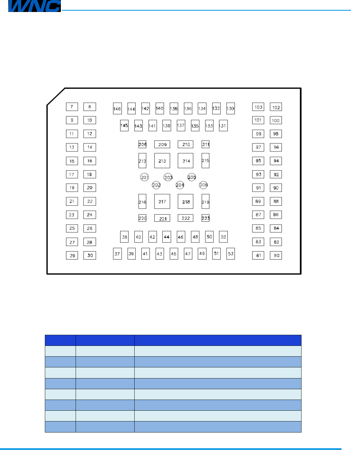
The IMS2 LGA module pin layout is illustrated below.
Figure 2-1. IMS2 LGA module pin layout
2.2 LGA Module Pin Definitions
The signals and all the related details are listed in the below table.
Table 2-1. IMS2 module pin definition
Pin No.
Name
Description
7
GND
Ground
8
GND
Ground
9
NC
Not connected
10
GND
Ground
11
GND
Ground
12
GND
Ground
13
GND
Ground
14
GND
Ground

Product datasheet
□ Normal □ Internal Use Confidential □ Restricted Confidential 9 / 29
15
Main antenna
Main antenna port
16
GND
Ground
17
GND
Ground
18
GND
Ground
19
GND
Ground
20
GND
Ground
21
NC
Not connected
22
GND
Ground
23
GND
Ground
24
GND
Ground
25
GND
Ground
26
GND
Ground
27
NC
Not connected
28
GND
Ground
29
GND
Ground
30
GND
Ground
37
Power
Power
38
Power
Power
39
Power
Power
40
Power
Power
41
Power
Power
42
Power
Power
43
NC
Not connected
44
GND
Ground
45
GND
Ground
46
GPIO46
General purpose input/output
47
GPIO47
General purpose input/output
48
GPIO48
General purpose input/output
49
GPIO49
General purpose input/output
50
GND
Ground
51
GND
Ground
52
GPIO01
General purpose input/output
53
GPIO02
General purpose input/output
80
UART1_CTS
Clear to send for UART 1
81
UART1_RTS
Request to send for UART 1
82
UART1_Rx
Receive for UART 1
83
UART1_Tx
Transmit for UART 1
84
GND
Ground
85
GND
Ground

Product datasheet
□ Normal □ Internal Use Confidential □ Restricted Confidential 10 / 29
86
NC
Not connected
87
NC
Not connected
88
NC
Not connected
89
GND
Ground
90
GND
Ground
91
GND
Ground
92
UART0_CTS
Clear to send for UART 0
93
UART0_TX
Transmit for UART 0
94
UART2_TX
Transmit for UART 2
95
UART0_RX
Receive for UART 0
96
UART2_RX
Receive for UART 2
97
UART0_RTS
Request to send for UART 0
98
UART2_RTS
Request to send for UART 2
99
UART2_CTS
Clear to send for UART 2
100
FFF/FFH mode
switch
FFF/FFH mode switch; FFF is normal mode; FFH is for
design mode.
101
RFDATA5
RF control interface
102
RFDATA6
RF control interface
103
RFDATA7
RF control interface
130
ADC
Analog-to-digital converter
131
ADC
Analog-to-digital converter
132
GPIO08
General purpose input/output
133
UIM_VCC
SIM card power
134
UIM DATA
SIM card data line
135
UIM CLK
SIM card clock line
136
UIM RESET
SIM card reset line
137
UIM DETECT
SIM card detect line
138
NC
Not connected
139
GND
Ground
140
GND
Ground
141
WWAN_STATE
Wireless WAN radio state
142
Power on
Power on the module
143
WAKEUP_OUT
Module wakes up host.
144
WAKEUP_IN
Host wakes up module.
145
RESET
Main reset line
146
VREF
Reference logic voltage (1.8 V voltage)
201
JTAG TCK
JTAG TCK
202
JTAG TDI
JTAG TDI
203
JTAG TDO
JTAG TDO

Product datasheet
□ Normal □ Internal Use Confidential □ Restricted Confidential 11 / 29
204
JTAG_TMS
JTAG_TMS
205
JTAG_SRST_N
JTAG_SRST_N
206
NC
Not connected
208
GND
Ground
209
GND
Ground
210
GND
Ground
211
GND
Ground
212
GND
Ground
213
GND
Ground
214
GND
Ground
215
GND
Ground
216
GND
Ground
217
GND
Ground
218
GND
Ground
219
GND
Ground
220
GND
Ground
221
GND
Ground
222
GND
Ground
223
GND
Ground
Product datasheet
□ Normal □ Internal Use Confidential □ Restricted Confidential 12 / 29
3 Electrical Specifications
3.1 Electrical Operating Conditions
3.1.1 Detailed Information
Table 3-1. Electrical operating conditions for the IMS2.
Direction
Minimum
Typical
Maximum
VCC
In
3.3 V
3.8 V
4.2 V
IMS2 includes an integrated Power Manager enabling single and direct voltage
supply from the battery and reducing the overall bill of materials.
Layout Suggestion: Each power trace should possess sufficient line width to
withstand its respective current listed in Table 3-2 below.
Table 3-2. Power supply reference currency
Net Name
Current Value
VCC(1–6) total
TBD
UIM_VCC
TBD
VREF
TBD
Note: Routing under a 1 A design is desired as it will result in more stable power.
3.1.2 Power Tree
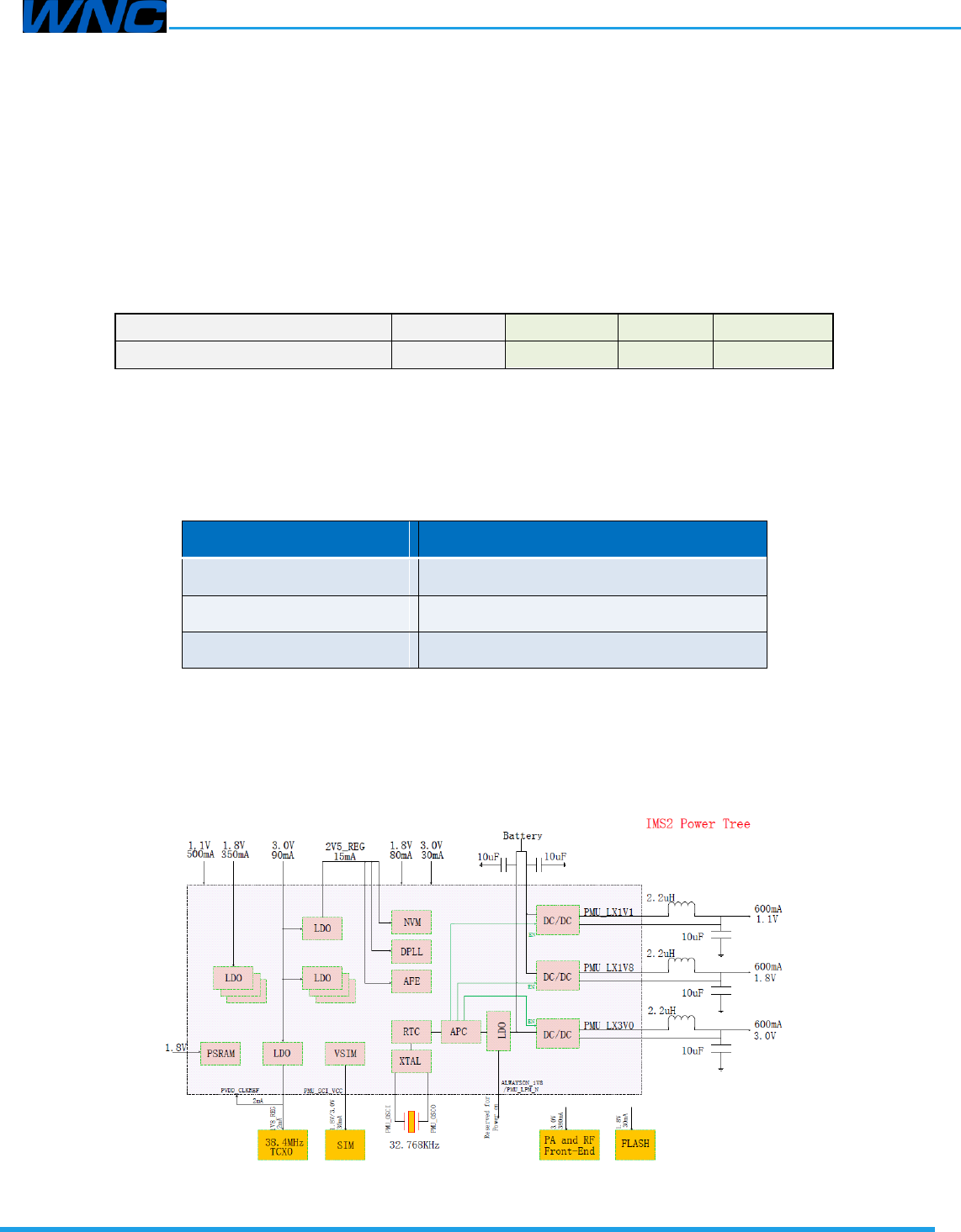
Figure 3-1 provides a representation of the power tree of the IMS2 LGA module
Figure 3-1. IMS2 power tree

Product datasheet
□ Normal □ Internal Use Confidential □ Restricted Confidential 13 / 29
3.2 Control Interfaces
This section describes the power-on/off, wake-up, and reset interface for controlling
the module.
3.2.1 Power-on Signal (TBD)
The POWER_ON signal is an active low input signal used to enable or disable the
module. Do not toggle the PERST# pin during power-on. This signal has the highest
priority among the wakeup, the alarm signal, and the digital control pins.
There are three possible states of the module:
• Module Off: VCC is not present.
• Module Enabled: VCC is supplied, and the module is enabled.
• Module Disabled: VCC is supplied, and the module is disabled.
The state transitions are defined as follows:
• When voltage is applied to VCC, the module shall enter the Module Disabled
state.
An input to the POWER_ON pin shall trigger the transition from the Module Disabled
to the Module Enabled state. See Figure 6; a low pulse (tlow > 0s) on the POWER_ON
pad will enable the module after VCC is applied.
3.2.2 Wake-up Interface (TBD)
In applications where power consumption is a major factor in performance metrics
(such as battery-operated sensors that are based on an IOT/M2M modem solution
and also include a third-party host), definitions are necessary for a simple interface
that will enable both the modem and the host to enter low-power states whenever
possible and the other side to wake it up once required.
For example, if the host has no data to transmit or any other tasks, it may enter a
low-power state according to its own capabilities and configurations. If during that
period the host is in a low-power state and the modem suddenly receives data, it
must wake-up the host.
A similar requirement exists in the reverse case. For example, if the modem is in a
low-power state and suddenly the host must transmit data, it must be able to wake-
up the modem.
The interface consists of two signals: One is triggered by the host and received by
the modem; the other is triggered by the modem and received by the host.
Each side can wake the other by toggling a wakeup signal high and enabling the
Product datasheet
□ Normal □ Internal Use Confidential □ Restricted Confidential 14 / 29
other side to activate sleep mode when not needed by toggling it low.
• “WAKEUP_IN” (Host: Output, Modem: Input):
• LOW: SoC does not require the MODEM (allowing it to sleep).
• HIGH: SoC requires the MODEM or acknowledges it is ready
following a wakeup request from the MODEM.
• “WAKEUP_OUT” (Host: Input, Modem: Output):
• LOW: The MODEM does not require the Host (allowing it to sleep).
• HIGH: The MODEM requires the Host or acknowledges it is ready
following a wakeup request from the SoC.
When the IMS2 module functions as a modem, keep WAKEUP_IN high before the
system boot process is complete. After the system boot, maintain WAKEUP_IN in a
low state. The WAKEUP_IN and WAKEUP_OUT operation in host mode will be
discussed according to product specifications.
3.2.3 Reset Signal
The Reset Signal is a hardware reset signal to control the system reset directly. The
user can connect it to a key or a control signal. A low pulse after power on will reset
the module.
3.3 UART Interface
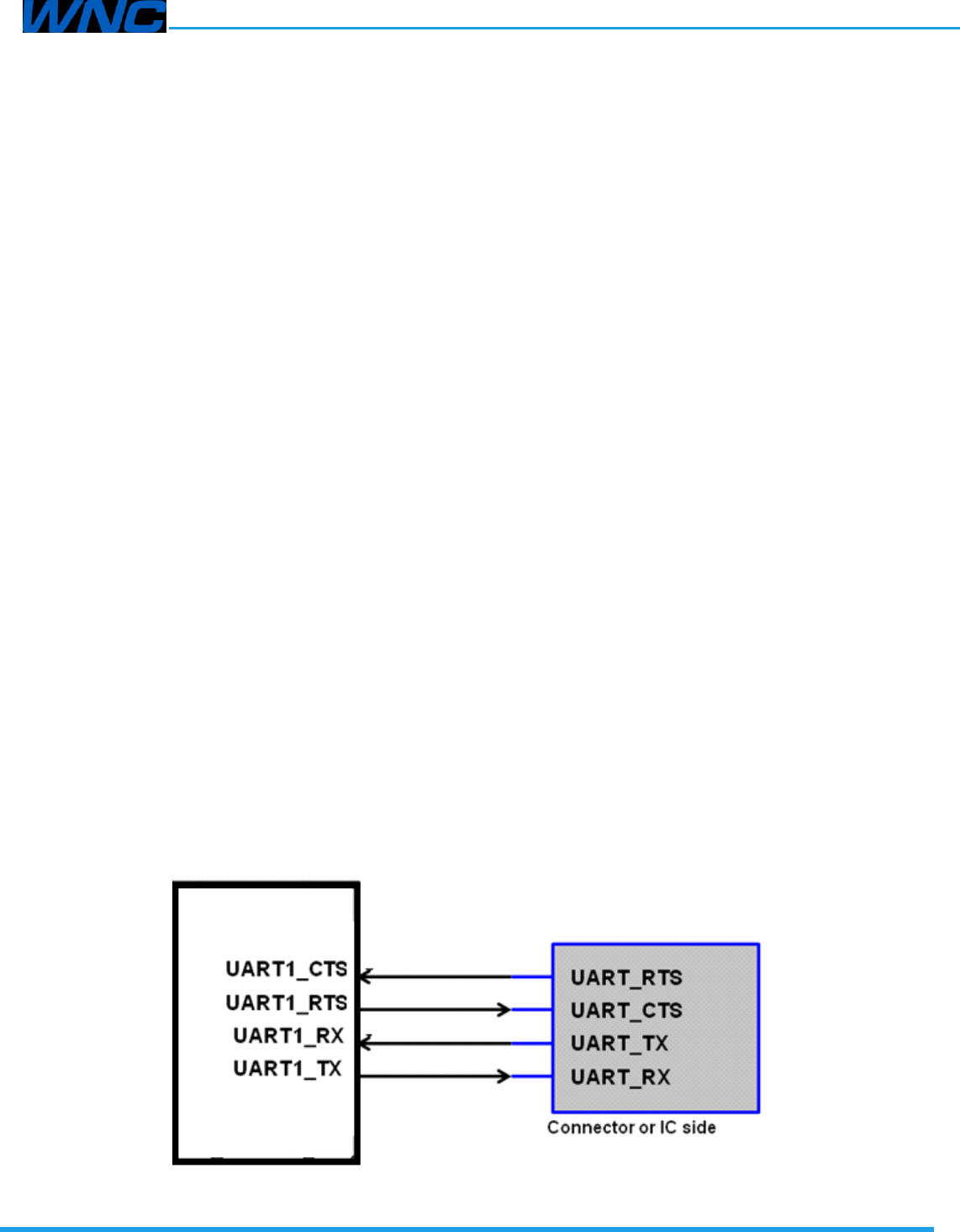
There are three UART interfaces; these interfaces are 4 bit for high-speed data
transfer, and the UART definitions of IMS2 are shown in Figure 3-2.
1. UART0 for data
2. UART1 for debugging the DM tool and software upgrade
3. UART2 for the console
Figure 3-2. UART connection (example)
Product datasheet
□ Normal □ Internal Use Confidential □ Restricted Confidential 15 / 29
3.4 UIM Interface
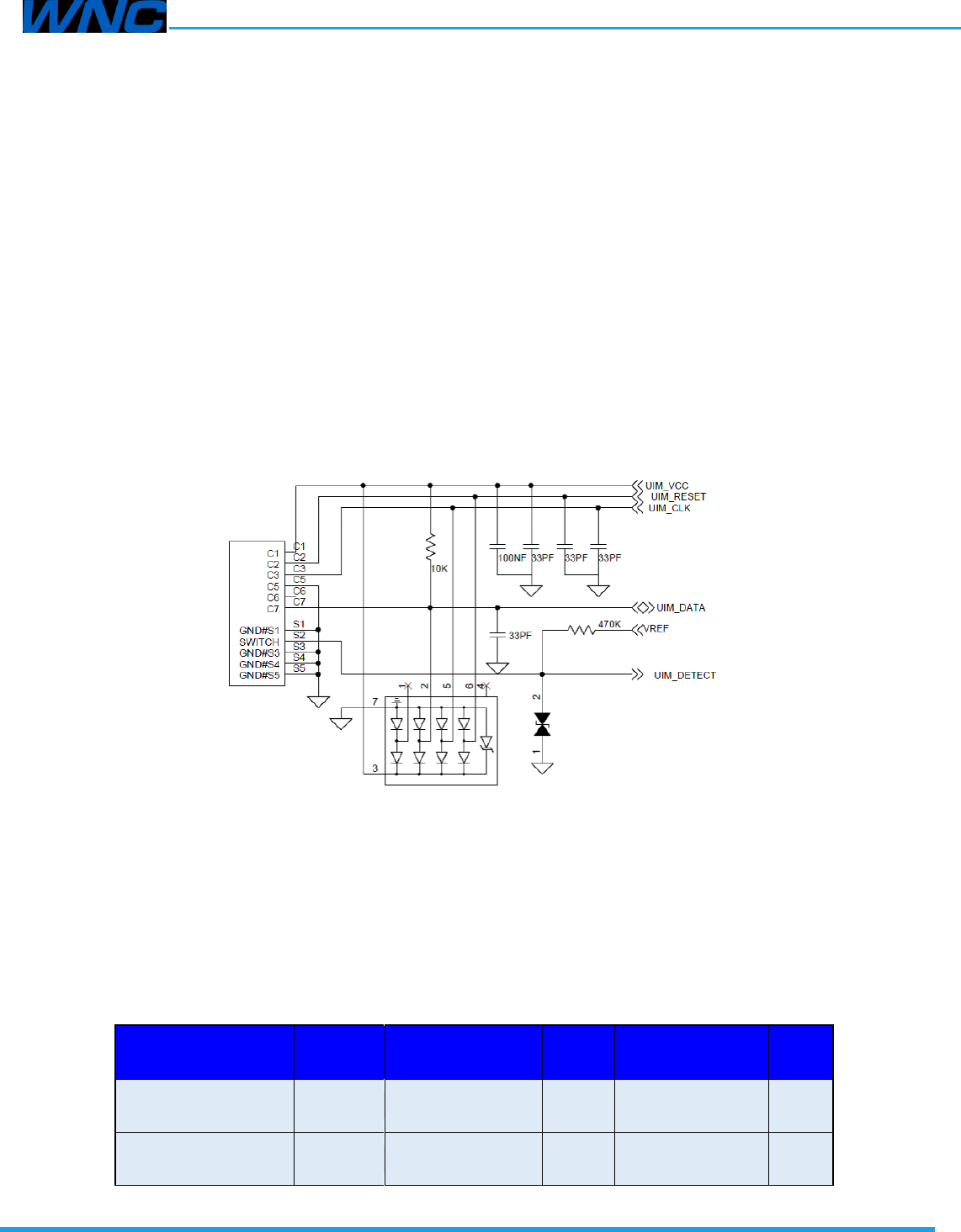
IMS2 modules provide a UIM_DETECT input pin for UIM connectors to detect a UIM
card. When a UIM card is present, UIM_DETECT should be high (1.8 V). If the UIM
card is absent, UIM_DETECT should be low. This is required to pull UIM_DETECT to
VREF with a 470 kΩ resistor. A 0.1 μF and a 33 pF capacitor are recommended to
place between UIM_VCC and Ground in parallel. We recommend placing a 33 pF
capacitor between UIM_RESET, UIM_CLK, and UIM_DATA and Ground in parallel.
(Refer to Figure 5.)
An electrostatic discharge (ESD) protection circuit is also recommended to place near
the UIM socket as close as possible, and the Ground pin of the ESD protection
component must be well connected to the Ground plane.
The following figure illustrates an example UIM card circuit. The default
configuration is active high.
Figure 3-3. Example UIM card circuit
3.5 I/O Characteristics
The voltage and current characteristics of the various IO pads of the IMS2 versus IO
bank supply voltage are illustrated in Table 3-3 below.
Table 3-3. DC characteristics for digital IOs, voltage 1.8 V - BIDIR and IN types
Parameter
Drive
Strength
Min.
Nom.
Max.
Unit
VIL
Input low voltage
VSS
0.3 × PVDD_1V8
V
VIH
Input high voltage
0.7 × PVDD_1V8
PVDD_1V8
V

Product datasheet
□ Normal □ Internal Use Confidential □ Restricted Confidential 16 / 29
VOL
Output low voltage
VSS
0.2 × PVDD_1V8
V
VOH
Output high
voltage
0.8 × PVDD_1V8
PVDD_1V8
V
IRPU
Input pull-up
resistor current
15
μA
RPU
Input pull-up
resistance
32.4
kΩ
IRPD
Input pull-down
resistor current
15
μA
RPD
Input pull-down
resistance
32.4
kΩ
VH
Input hysteresis
0.1 × PVDD_1V8
V
IPAD
Input leakage
current, non-
tolerant
–1
1
μA
IOZ
Off-state leakage
current
1
μA
IOL
Sink current at
VOL (max)
2 mA
1.11
mA
4 mA
2.25
mA
8 mA
4.48
mA
12 mA
6.72
mA
IOH
Source current at
VOH (max)
2 mA
1.1
mA
4 mA
2.2
mA
8 mA
4.4
mA
12 mA
6
.
6
m
A
Product datasheet
□ Normal □ Internal Use Confidential □ Restricted Confidential 17 / 29
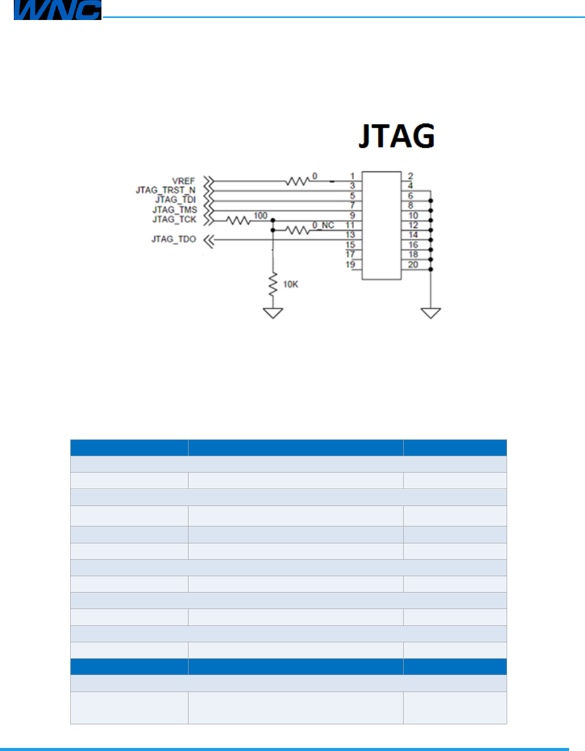
3.6 JTAG Interface
The IMS2 series contains one JTAG interface; leave JTAG pins floating if they are
not used.
Figure 3-4. JTAG schematic
3.7 Power Consumption
This section describes the typical power consumption of the IMS2 (for reference).
Table 3-4. LTE power consumption
Working Mode
Conditions
Result
Airplane mode
Only the module; no other devices
TBD
Power saving mode
TBD
TBD
TBD
TBD
TBD
TBD
LTE Band2 working mode
TBD
TBD
LTE Band4 working mode
TBD
TBD
LTE Band12 working mode
TBD
TBD
Powering on
Conditions
Result
Peak power consumption
Power consumption peak when the
module is powering on
TBD
Product datasheet
□ Normal □ Internal Use Confidential □ Restricted Confidential 18 / 29
Power off
Conditions
Result
Power off consumption
The module is powered off.
TBD
3.8 RF Performance
Each IMS2 module has only one RF pad; developers must connect it via 50 Ω traces
to the main board.
Main antenna pad (Pin15) – Primary RX/TX path
3.8.1 RF Pad Design
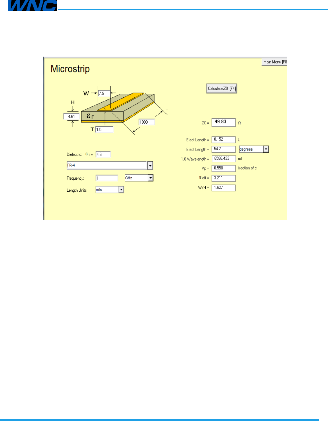
We recommended that a ground not be present under the surface of the RF pads in
the layout. Details are included below. Layer2 has the same exclusion area as Layer1.
Figure 3-5. Sample RF pad layout
Product datasheet
□ Normal □ Internal Use Confidential □ Restricted Confidential 19 / 29
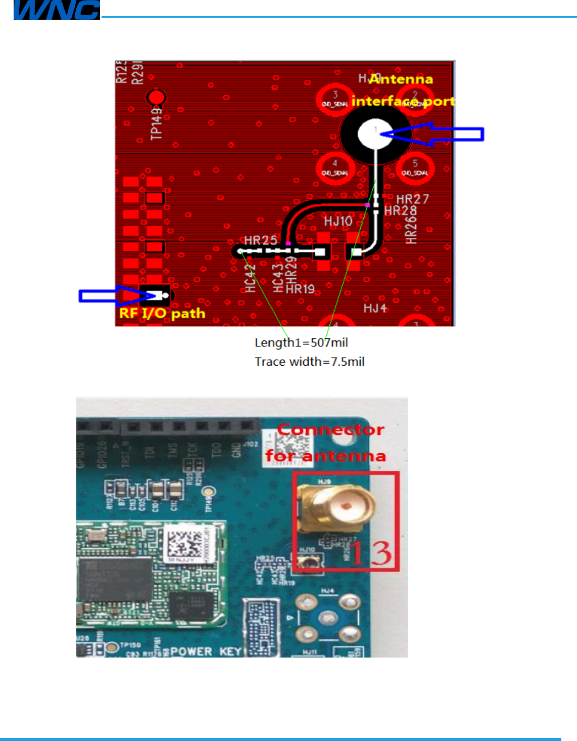
The RF trace between RF pads and antenna should as shorter as possible with 50ohm
characteristic impedance.
The characteristic impedance depends on the dielectric of PCB, the track width and
the ground plane spacing. Microstrip type is required. The detail simulation as below.
Product datasheet
□ Normal □ Internal Use Confidential □ Restricted Confidential 20 / 29
The antenna should be 50ohm characteristic impedance with the return loss of
better than -10dB at the operation band. The antenna gain would affect the radiated
power and regulator test result.
Product datasheet
□ Normal □ Internal Use Confidential □ Restricted Confidential 21 / 29
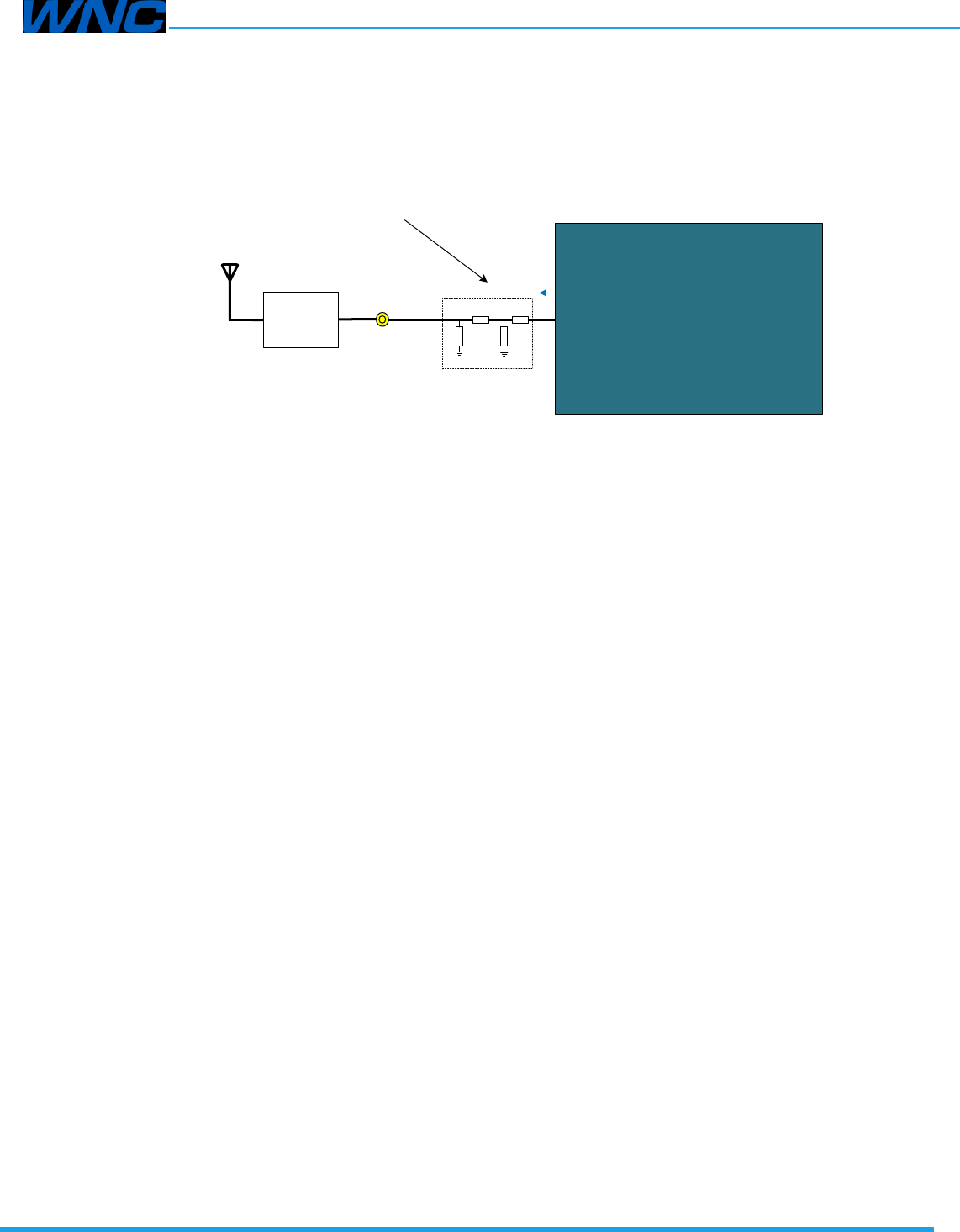
3.8.2 RF Matching Guide
IMS2
module
Primary
Antenna
Pin15 RF_1
Antenna
matching
RF connector
1. Reserve the matching circuit as
depicted in the topological structure
below.
2. The matching circuit should be as close
to the module as possible.
The impedance (S11) should be close to
50 Ω, VSWR < 1.5.
Figure 3-6. RF matching guide
3.8.3 Interference and Sensitivity
This section includes tips to help developers identify interferences that may affect
the IMS2 module when used in systems.
Interference from other wireless devices
– Harmonics, inter-modulated signals generated from wireless devices
within the RX ranges of the modules may result in degraded RX
performance.
– We highly recommend checking the RX performance of entire
systems within the shielding environment.
Interference from the host interface
– High-speed signal-switching elements in systems can easily couple
noise into the module (ex.: DDR memory, LCD modules, DC-DC
converters, PCM signals).
Methods to avoid sources of interference
– Antenna location is important; we recommend directing the
antenna away from high-speed switching signals. Furthermore, the
trace from the module to the antenna should be as short as possible
and must be shielded by complete grounding.
– The IMS2 module is well shielded; high-speed elements (Ex.: DDR
memory, LCD modules, DC-to-DC converters, PCM signals) on a
system should have shielding reserved during the early stages of
development.
Product datasheet
□ Normal □ Internal Use Confidential □ Restricted Confidential 22 / 29
3.8.4 Band Support
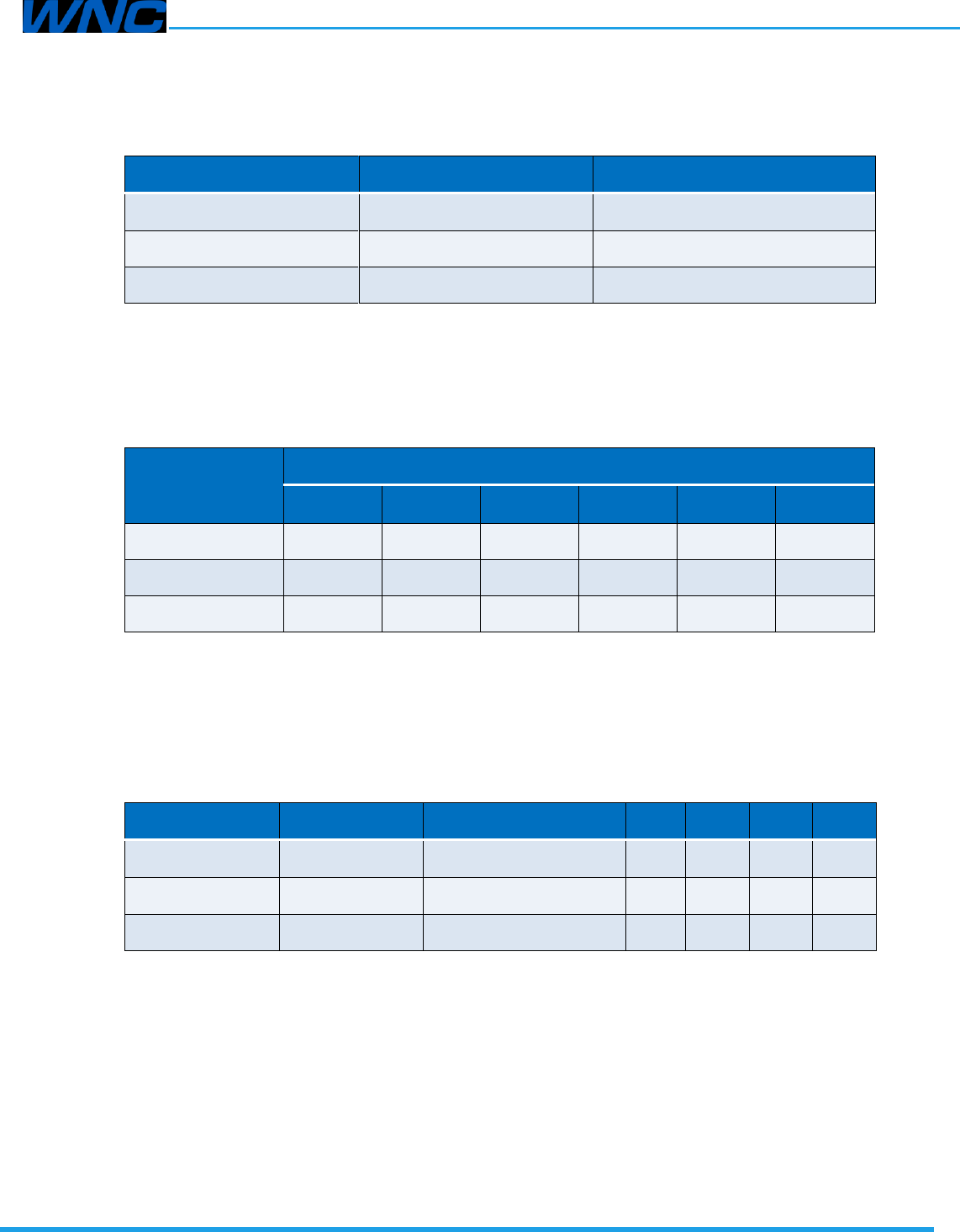
Table 3-5. Band support
Band
Uplink (MHz)
Downlink (MHz)
LTE Band 2
1,850–1,910
1,930–1,990
LTE Band 4
1,710–1,755
2,110–2,155
LTE Band 12
699–716
729–746
3.8.5 Bandwidth Support
Table 3-6. Bandwidth support
Band
Bandwidth
1.4 MHz
3 MHz
5 MHz
10 MHz
15 MHz
20 MHz
LTE Band 2
-
-
LTE Band 4
-
-
LTE Band 12
-
-
-
-
Note: The IMS2 supports 1.4 MHz and 3 MHz (not default settings).
3.8.6 RF Transmission Specifications
Table 3-7. Conductive Tx output power
Band
Items
Parameter
Unit
Min.
Typ.
Max.
LTE Band 2
Max. TX Power
20 MHz 1 RBs/QPSK
dBm
20.3
23
25.7
LTE Band 4
Max. TX Power
20 MHz 1 RBs/QPSK
dBm
20.3
23
25.7
LTE Band 12
Max. TX Power
10 MHz 1 RBs/QPSK
dBm
20.3
23
25.7
Notes: 1.The RF transmission specification is defined at the LGA pad.
2. IMS2 fulfills 3GPP test standards.

Product datasheet
□ Normal □ Internal Use Confidential □ Restricted Confidential 23 / 29
3.8.7 RF Receiver Specifications
Table 3-7. Conductive Rx sensitivity-3GPP
Band
Items
Parameter
Unit
Min.
Typ.
Max.
L
T
E
B
a
n
d
2
R
X
S
e
n
s
i
t
i
v
i
t
y
5
M
Hz
wit
h 4
RB
s
d
B
m
–99.5
LTE Band 4
RX Sensitivity
5 MHz with 4 RBs
dBm
–101.5
LTE Band 12
RX Sensitivity
5 MHz with 4 RBs
dBm
–98.5
Notes: 1. The RF receiver specification is defined at the LGA pad.
2. IMS2 fulfills 3GPP test standards.
3.9 Temperature
• 3GPP compliance: –20 °C to +60 °C (ambient)
• Functional: –40 °C to +85 °C
• Storage: –40 °C to +85 °C
3.10 LTE Power Saving Mode
Note: Details will be provided in a future revision of this document.
3.11 Serial Number and IMEI
Serial number and IMEI data can be written to the module only once; these two data

Product datasheet
□ Normal □ Internal Use Confidential □ Restricted Confidential 24 / 29
points cannot be rewritten on the SQN3330 platform.
Product datasheet
□ Normal □ Internal Use Confidential □ Restricted Confidential 25 / 29
4 Mechanical Information
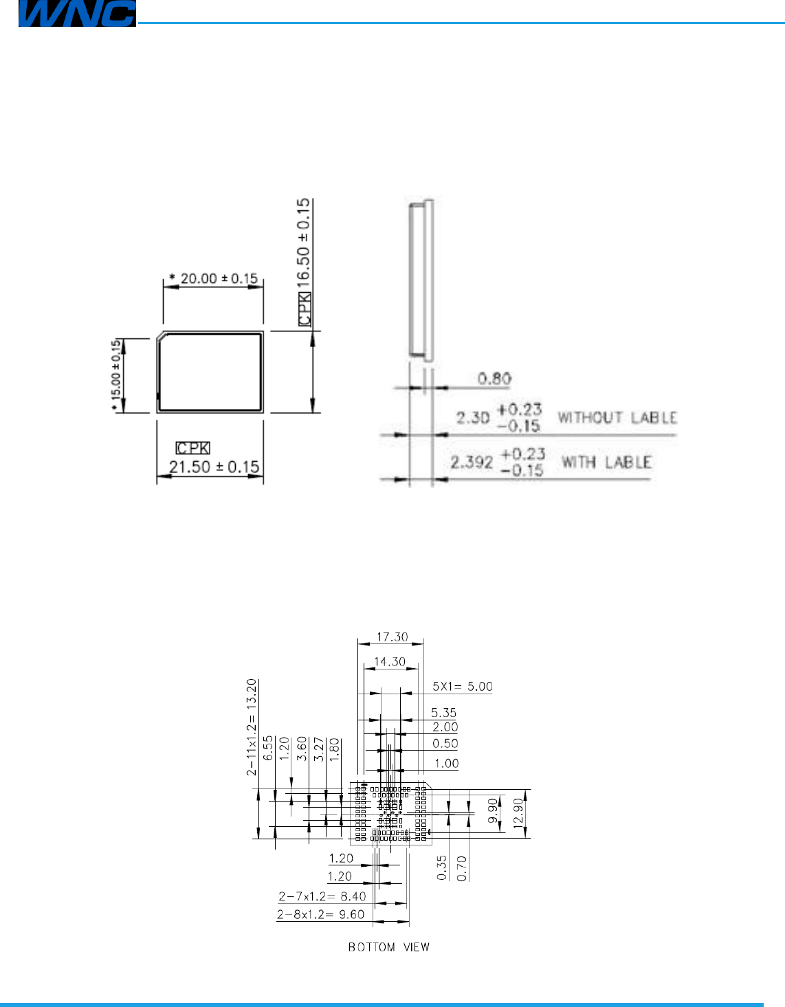
4.1 Physical Dimensions
Device dimensions illustrated in Figure 4-1 and Figure 4-2 below.
Figure 4-1. Top view
Figure 4-2. Right view
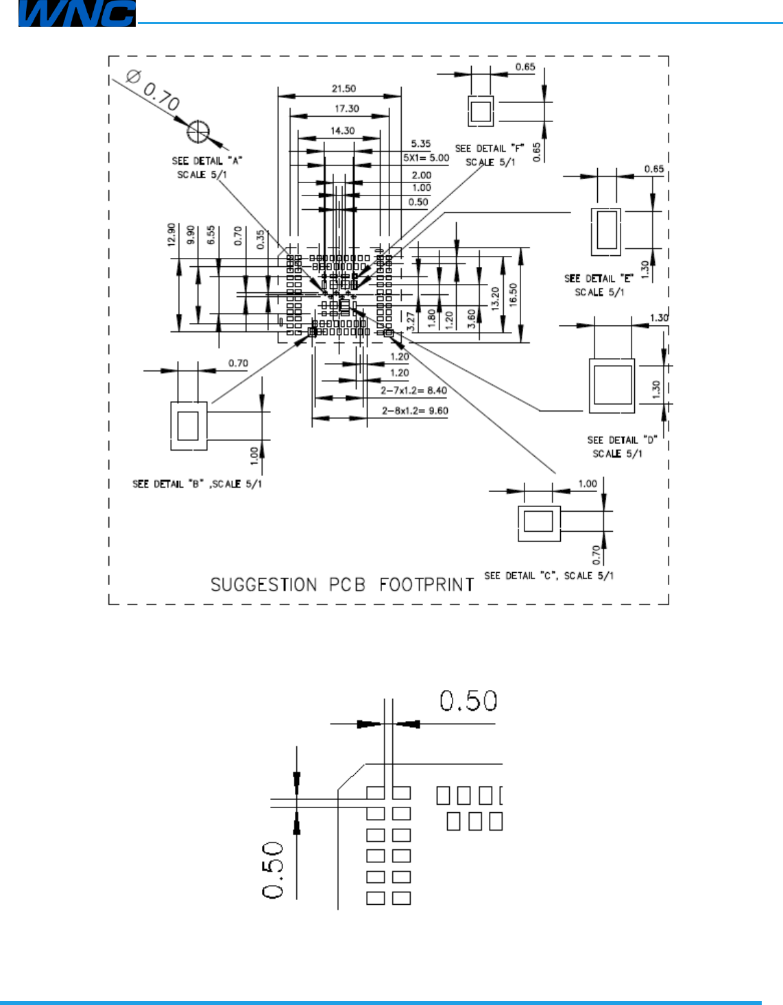
4.2 Pin Dimensions
The dimensions are illustrated in Figure 4-3, Figure 4-4, and Figure 4-5 below.
Figure 4-3. PIN dimensions (bottom view)
Product datasheet
□ Normal □ Internal Use Confidential □ Restricted Confidential 26 / 29
Figure 4-4. PIN dimensions
Figure 4-5. PIN dimensions

Product datasheet
□ Normal □ Internal Use Confidential □ Restricted Confidential 27 / 29
4.3 Marking Information
Note: Details will be provided in a future version of this document.

Product datasheet
□ Normal □ Internal Use Confidential □ Restricted Confidential 28 / 29
5 Packing Information
5.1 Packing Information
The module is delivered in tape-and-reel based on MPQ.
Note: Module packing details will be provided in a future revision of this document.
5.2 Storage Conditions
Note: Details will be provided in a future revision of this document.
6 PCB Mounting Guidelines
6.1 Mounting Considerations
This section details the recommended reflow profile when the module is mounted
onto other boards.
Note: Details will be provided in a future revision of this document.
7 Regulatory and Industry Approval
7.1 Certification Testing
PTCRB, FCC, and AT&T TA
7.2 GP Compliance
RoHS (2011/65/EU)

Product datasheet
□ Normal □ Internal Use Confidential □ Restricted Confidential 29 / 29
Initialisms
Initialisms and Definitions
Initialism
Definition
AC
Alternating Current
DC
Direct Current
ETSI
European Telecommunications Standards Institute
GND
Ground
GPIO
General Purpose Input Output
I/O
Input/Output
IoT
Internet of Things
I2C
Inter-Integrated Circuit
LGA
Land Grid Array
LTE
Long Term Evolution
N/A
Not/Applicable
OS
Operating System
PIN
Personal Identification Number
SIM
Subscriber Identity Module
SPI
Serial Peripheral Interface
UART
Universal Asynchronous Receiver-Transmitter
UIM
User Identity Module
USB
Universal Serial Bus
Vref
Voltage reference
WNC
Wistron NeWeb Corporation