Wistron NeWeb XRBH-1 BLE Module User Manual XRBH 1 BLE module V04
Wistron NeWeb Corporation BLE Module XRBH 1 BLE module V04
UserManual.wiki
>
Wistron NeWeb
>
XRBH 1 User Manual
User manual
Navigation menu
Upload a User Manual
Namespaces
Wiki Guide
HTML
PDF
Info
Views
User Manual
Discussion / Help
Navigation
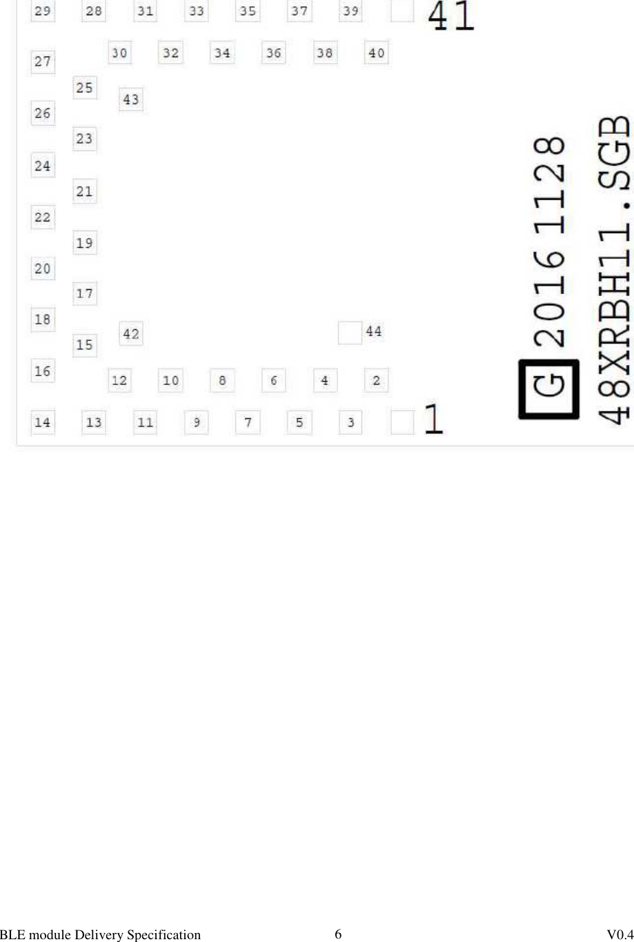
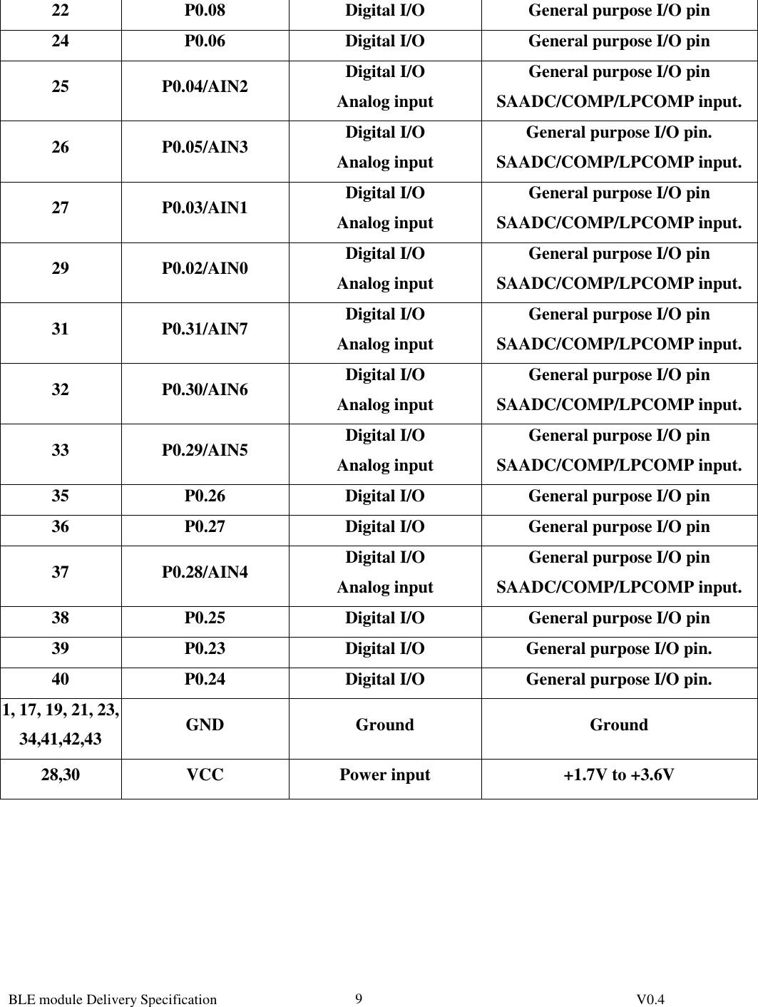
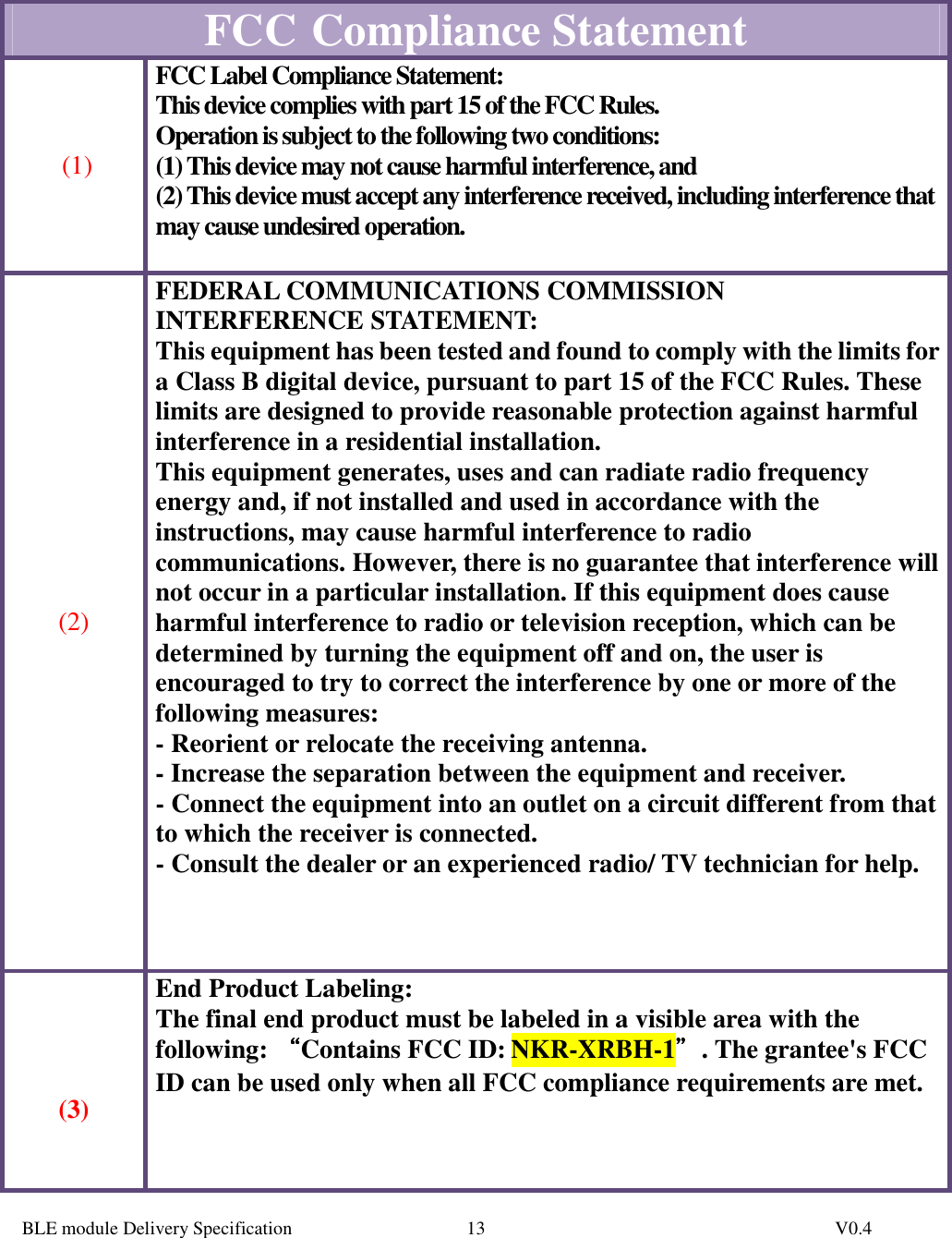
![BLE module Delivery Specification V0.4 8PIN Define Pin number Name Function Description 2 SWCLK Digital input Serial Wire Debug clock input for debug and programming. 3 SWDIO Digital I/O Serial Wire Debug I/O for debug and programming. 4 P0.21/RESET Digital I/O General purpose I/O pin. Configurable as pin reset. 5 P0.22 Digital I/O General purpose I/O pin. 6 P0.20/ TRACECLK Digital I/O General purpose I/O pin. Trace port clock output. 7 P0.18/ TRACEDATA[0] Digital I/O General purpose I/O pin. Trace port output. Single Wire Output. 8 P0.19 Digital I/O General purpose I/O pin. 9 P0.17 Digital I/O General purpose I/O pin. 10 P0.16/ TRACEDATA[1] Digital I/O General purpose I/O pin. Trace port output. 11 P0.11 Digital I/O General purpose I/O pin 12 P0.13 Digital I/O General purpose I/O pin 13 P0.15/ TRACEDATA[2] Digital I/O General purpose I/O pin. Trace port output. 14 NFC2/P0.10 NFC input Digital I/O NFC antenna connection. General purpose I/O pin 15 P0.14/ TRACEDATA[3] Digital I/O General purpose I/O pin. Trace port output. 16 P0.12 Digital I/O General purpose I/O pin 18 NFC1/P0.09 NFC input Digital I/O NFC antenna connection. General purpose I/O pin 20 P0.07 Digital I/O General purpose I/O pin](https://usermanual.wiki/Wistron-NeWeb/XRBH-1/User-Guide-3389570-Page-9.png)