Wistron B6Z400 Bluetooth Stereo ROM Module Board User Manual B6Z 400 A1 DataSheet
Wistron Corporation Bluetooth Stereo ROM Module Board B6Z 400 A1 DataSheet
UserManual.wiki
>
Wistron
>
B6Z400 User Manual
Users Manual
Navigation menu
Upload a User Manual
Namespaces
Wiki Guide
HTML
PDF
Info
Views
User Manual
Discussion / Help
Navigation
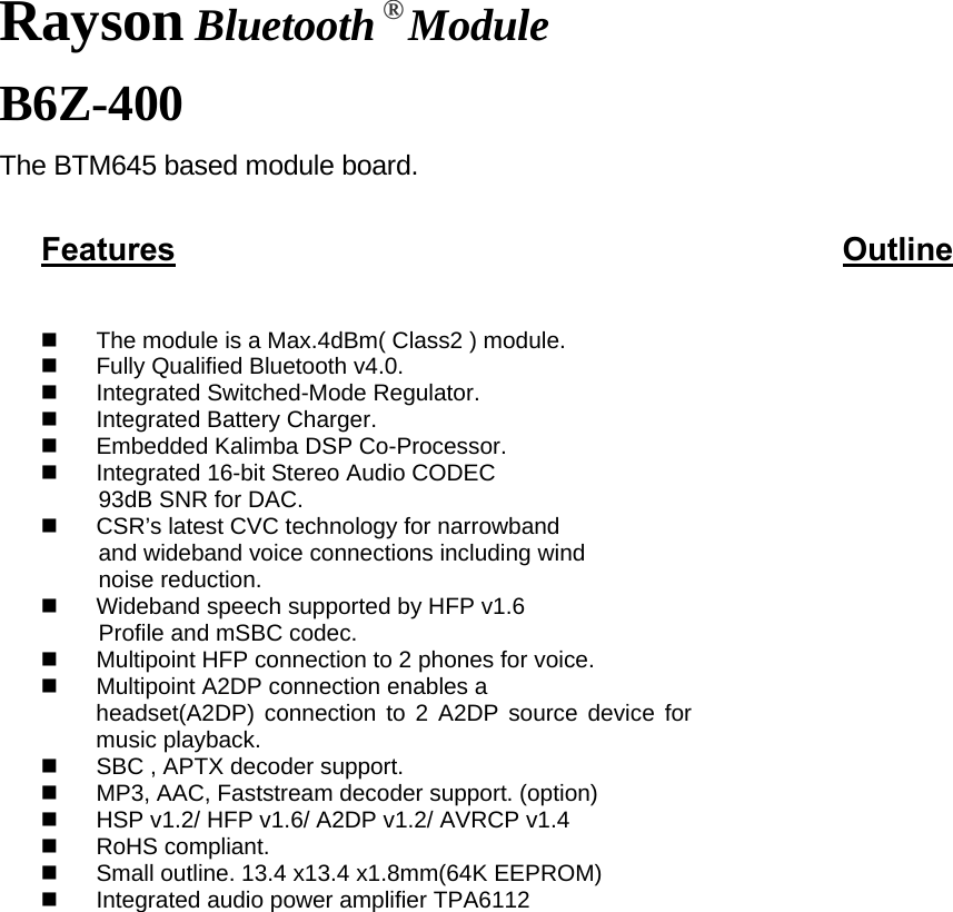
![General Electrical Specification Absolute Maximum Ratings: Ratings Min. Max. Storage Temperature -40 ℃ +85 ℃ Supply Voltage (VCHG) -0.4V 5.75V Supply Voltage (VREG_ENABLE,VBAT_SENSE) -0.4V 4.2V Supply Voltage (LED[2:0]) -0.4V 4.4V Supply Voltage (PIO_POWER) -0.4V 3.6V Recommended Operating Condition: Operating Condition Operating Temperature range -20 ℃ +75 ℃ Supply Voltage (VBAT) 2.7V 4.25V Supply Voltage (VCHG) 4.75V / 3.10 V 5.25V Supply Voltage (VREG_ENABLE,VBAT_SENSE) 0V 4.2V Supply Voltage (LED[2:0]) 1.10V 4.25V Supply Voltage (PIO_POWER)* 1.7V 3.6V Regulator Enable VREG_ENABLE, Switching Threshold Min Typ Max Unit Rising threshold 1.0 - - V (a) superseded electrical characteristics are listed in this table. Stereo Codec: Analogue to Digital Converter Analogue to Digital Converter Parameter Conditions Min Typ Max Unit Resolution - - - 16 Bits Input Sample Rate, Fsample - 8 - 48 kHz Fsample 8kHz - 89 - dB 16kHz - 85 - dB 32kHz - 85 - dB 44.1kHz - 85 - dB SNR fin = 1kHz B/W = 20Hz→Fsample/2 (20kHz max) A-Weighted THD+N < 1% 1.6Vpk-pk input 48kHz - 85 - dB](https://usermanual.wiki/Wistron/B6Z400/User-Guide-2040412-Page-4.png)
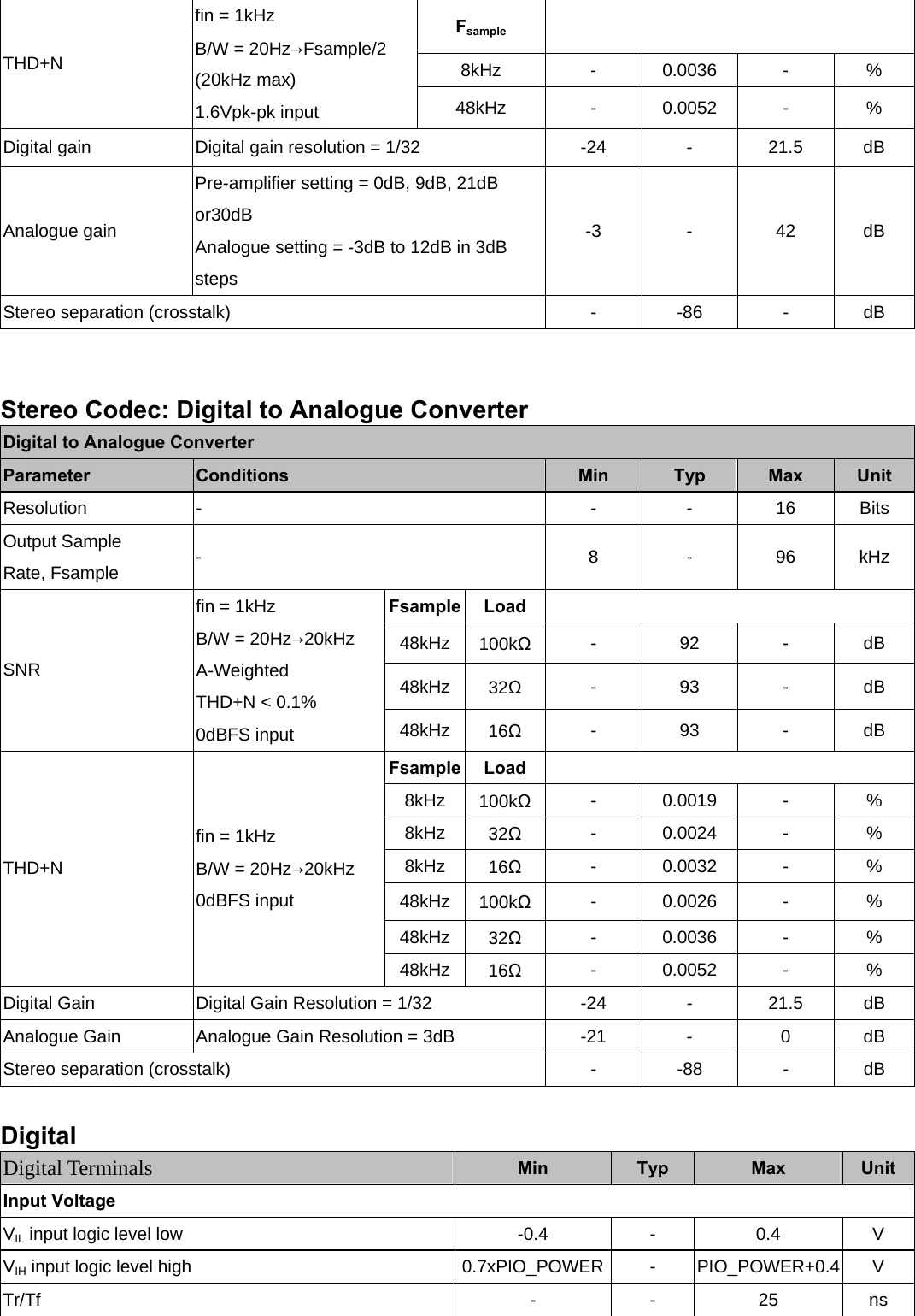
![Interfaces Analogue I/O Ports, AIO B6Z-400 has 1 general-purpose analogue interface pin, AIO[0]. Typically, this connects to a thermistor for battery pack temperature measurements during charge control. LED Drivers B6Z-400 includes a 3-pad synchronised PWM LED driver for driving RGB LEDs for producing a wide range of colours. All LEDs are controlled by firmware. The terminals are open-drain outputs, so the LED must be connected from a positive supply rail to the pad in series with a current-limiting resistor. Figure 2.1: LED Equivalent Circuit From Figure 2.1 it is possible to derive Equation 2.1 to calculate ILED. If a known value of current is required through the LED to give a specific luminous intensity, then the value of RLED is calculated. Equation 2.1: LED Current For the LED pads to act as resistance, the external series resistor, RLED, needs to be such that the voltage drop across it, VR, keeps VPAD below 0.5V. Equation 2.2 also applies. VDD = VF + VR + VPAD Equation 2.2: LED PAD Voltage Note: The LED current adds to the overall current. Conservative LED selection extends battery life. Reset, RST# B6Z-400 is reset from several sources: ■ RST# pin ■ Power-on reset ■ USB charger attach reset](https://usermanual.wiki/Wistron/B6Z400/User-Guide-2040412-Page-11.png)
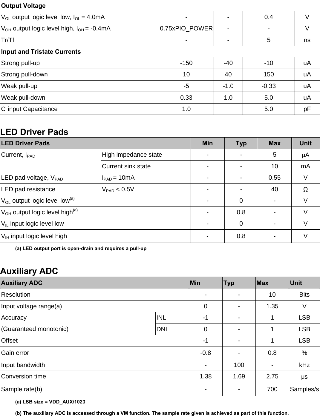
![■ Software configured watchdog timer The RST# pin is an active low reset and is internally filtered using the internal low frequency clock oscillator. Rayson recommends applying RST# for a period >5ms. At reset the digital I/O pins are set to inputs for bidirectional pins and outputs are set to tristate. Digital Pin States on Reset Table 3.3.1 shows the pin states of B6Z-400 on reset. Pin Name / Group I/O Type Full Chip Reset USB_DP Digital bidirectional N/A USB_DN Digital bidirectional N/A PIO[0] Digital bidirectional PUS PIO[1] Digital bidirectional PUS PIO[2] Digital bidirectional PDW PIO[3] Digital bidirectional PDW PIO[4] Digital bidirectional PDW PIO[5] Digital bidirectional PDW PIO[6] Digital bidirectional PDS PIO[7] Digital bidirectional PDS PIO[8] Digital bidirectional PUS PIO[9] Digital bidirectional PDS PIO[16] Digital bidirectional PUS PIO[17] Digital bidirectional PDS PIO[18] Digital bidirectional PDW PIO[19] Digital bidirectional PDW PIO[20] Digital bidirectional PDW PIO[21] Digital bidirectional PDW Table 3.3.1: Pin States on Reset Note: PUS = Strong pull-up PDS = Strong pull-down PUW = Weak pull-up PDW = Weak pull-down](https://usermanual.wiki/Wistron/B6Z400/User-Guide-2040412-Page-12.png)