Wistron B6Z400 Bluetooth Stereo ROM Module Board User Manual B6Z 400 A1 DataSheet
Wistron Corporation Bluetooth Stereo ROM Module Board B6Z 400 A1 DataSheet
Wistron >
Users Manual

Rayson
1F No.9 R&D Rd.II ,Science-Based Industrial Park,Hsin-Chu 300 Taiwan,R.O.C.
No.1,Tongfu 1
ST Road ,The 2nd Industrial Zone, Loucun, Gongming, Guangming
New District, Shenzhen, China.
Tel: 886-3-5633666 Fax: 886-3-5633688
Email: sales@.rayson.com
文件編號:
Approval Sheet Date :
2-July-2013
Customer Wistron
Part Number
Description Bluetooth Stereo ROM Module Board
Customer’s Project Sound Bar system
Manufacturer Rayson Technology Co., Ltd
Model Name B6Z-400_A1
Supplier Level:■New Source □Second Source
Contact Person: Tel: +886-3-5633666
Approval status :
E.E. engineer: ■Approval □Reject
M.E. engineer: □Approval □Reject
P.E. engineer: □Approval □Reject
Approval:
Accessories:
■ Specification ■ Sample □ Drawing □ Test Report
□ AT Command sets □ Packing Diagram

Document History
Revision Date Change Reason
1 2013-4-16 Draft
2 2013-7-2 Add two Tan-Capacitor to A1 Revision

Rayson Bluetooth ® Module
B6Z-400
The BTM645 based module board.
Features Outline
The module is a Max.4dBm( Class2 ) module.
Fully Qualified Bluetooth v4.0.
Integrated Switched-Mode Regulator.
Integrated Battery Charger.
Embedded Kalimba DSP Co-Processor.
Integrated 16-bit Stereo Audio CODEC
93dB SNR for DAC.
CSR’s latest CVC technology for narrowband
and wideband voice connections including wind
noise reduction.
Wideband speech supported by HFP v1.6
Profile and mSBC codec.
Multipoint HFP connection to 2 phones for voice.
Multipoint A2DP connection enables a
headset(A2DP) connection to 2 A2DP source device for
music playback.
SBC , APTX decoder support.
MP3, AAC, Faststream decoder support. (option)
HSP v1.2/ HFP v1.6/ A2DP v1.2/ AVRCP v1.4
RoHS compliant.
Small outline. 13.4 x13.4 x1.8mm(64K EEPROM)
Integrated audio power amplifier TPA6112

General Electrical Specification
Absolute Maximum Ratings:
Ratings Min. Max.
Storage Temperature -40 ℃ +85 ℃
Supply Voltage (VCHG) -0.4V 5.75V
Supply Voltage (VREG_ENABLE,VBAT_SENSE) -0.4V 4.2V
Supply Voltage (LED[2:0]) -0.4V 4.4V
Supply Voltage (PIO_POWER) -0.4V 3.6V
Recommended Operating Condition:
Operating Condition
Operating Temperature range -20 ℃ +75 ℃
Supply Voltage (VBAT) 2.7V 4.25V
Supply Voltage (VCHG) 4.75V / 3.10 V 5.25V
Supply Voltage (VREG_ENABLE,VBAT_SENSE) 0V 4.2V
Supply Voltage (LED[2:0]) 1.10V 4.25V
Supply Voltage (PIO_POWER)* 1.7V 3.6V
Regulator Enable
VREG_ENABLE, Switching Threshold Min Typ Max Unit
Rising threshold 1.0 - - V
(a) superseded electrical characteristics are listed in this table.
Stereo Codec: Analogue to Digital Converter
Analogue to Digital Converter
Parameter Conditions Min Typ Max Unit
Resolution - - - 16 Bits
Input Sample Rate,
Fsample - 8 - 48 kHz
Fsample
8kHz - 89 - dB
16kHz - 85 - dB
32kHz - 85 - dB
44.1kHz - 85 - dB
SNR
fin = 1kHz
B/W = 20Hz→Fsample/2
(20kHz max)
A-Weighted
THD+N < 1%
1.6Vpk-pk input 48kHz - 85 - dB

Fsample
8kHz - 0.0036 - %
THD+N
fin = 1kHz
B/W = 20Hz→Fsample/2
(20kHz max)
1.6Vpk-pk input 48kHz - 0.0052 - %
Digital gain Digital gain resolution = 1/32 -24 - 21.5 dB
Analogue gain
Pre-amplifier setting = 0dB, 9dB, 21dB
or30dB
Analogue setting = -3dB to 12dB in 3dB
steps
-3 - 42 dB
Stereo separation (crosstalk) - -86 - dB
Stereo Codec: Digital to Analogue Converter
Digital to Analogue Converter
Parameter Conditions Min Typ Max Unit
Resolution - - - 16 Bits
Output Sample
Rate, Fsample - 8 - 96 kHz
Fsample Load
48kHz 100kΩ- 92 - dB
48kHz 32Ω - 93 - dB
SNR
fin = 1kHz
B/W = 20Hz→20kHz
A-Weighted
THD+N < 0.1%
0dBFS input 48kHz 16Ω - 93 - dB
Fsample Load
8kHz 100kΩ- 0.0019 - %
8kHz 32Ω - 0.0024 - %
8kHz 16Ω - 0.0032 - %
48kHz 100kΩ- 0.0026 - %
48kHz 32Ω - 0.0036 - %
THD+N
fin = 1kHz
B/W = 20Hz→20kHz
0dBFS input
48kHz 16Ω - 0.0052 - %
Digital Gain Digital Gain Resolution = 1/32 -24 - 21.5 dB
Analogue Gain Analogue Gain Resolution = 3dB -21 - 0 dB
Stereo separation (crosstalk) - -88 - dB
Digital
Digital Terminals Min Typ Max Unit
Input Voltage
VIL input logic level low -0.4 - 0.4 V
VIH input logic level high 0.7xPIO_POWER - PIO_POWER+0.4 V
Tr/Tf - - 25 ns

Output Voltage
VOL output logic level low, IOL = 4.0mA - - 0.4 V
VOH output logic level high, IOH = -0.4mA 0.75xPIO_POWER - - V
Tr/Tf - - 5 ns
Input and Tristate Currents
Strong pull-up -150 -40 -10 uA
Strong pull-down 10 40 150 uA
Weak pull-up -5 -1.0 -0.33 uA
Weak pull-down 0.33 1.0 5.0 uA
CI input Capacitance 1.0 5.0 pF
LED Driver Pads
LED Driver Pads Min Typ Max Unit
High impedance state - - 5 μA
Current, IPAD
Current sink state - - 10 mA
LED pad voltage, VPAD I
PAD = 10mA - - 0.55 V
LED pad resistance VPAD < 0.5V - - 40 Ω
VOL output logic level low(a) - 0 - V
VOH output logic level high(a) - 0.8 - V
VIL input logic level low - 0 - V
VIH input logic level high - 0.8 - V
(a) LED output port is open-drain and requires a pull-up
Auxiliary ADC
Auxiliary ADC Min Typ Max Unit
Resolution - - 10 Bits
Input voltage range(a) 0 - 1.35 V
INL -1 - 1 LSB Accuracy
(Guaranteed monotonic) DNL 0 - 1 LSB
Offset -1 - 1 LSB
Gain error -0.8 - 0.8 %
Input bandwidth - 100 - kHz
Conversion time 1.38 1.69 2.75 μs
Sample rate(b) - - 700 Samples/s
(a) LSB size = VDD_AUX/1023
(b) The auxiliary ADC is accessed through a VM function. The sample rate given is achieved as part of this function.

Power Consumption
DUT Role Connection Packet Type Packet Size Average
Current
Unit
Slave SCO HV3 30 11.0 mA
Slave eSCO EV3 30 11.8 mA
Slave eSCO 2EV3 60 9.2 mA
Slave SCO 2-mic CVC HV3 30 12.6 mA
Slave eSCO 2-mic CVC 2EV3 60 10.8 mA
Slave eSCO 2-mic CVC 2EV3 60 11.4 mA
Slave
Stereo high quality SBC:
■ SBC
■ 48KHz sampling
■ No sniff
13.3 mA
Slave
Stereo high quality:
■ MP3
■ 48KHz sampling
■ No sniff
12.5 mA
Slave ACL Sniff = 500ms - - 213 mA
Slave ACL Sniff = 1280ms - - 142 mA
Master SCO HV3 30 10.8 mA
Master eSCO EV3 30 11.2 mA
Master eSCO 2EV3 60 8.8 mA
Master SCO 2-mic CVC HV3 30 12.5 mA
Master eSCO 2-mic CVC 2EV3 60 10.5 mA
Master eSCO 2-mic CVC 2EV3 60 11.0 mA
Note:
Current consumption values are taken with:
■ VBAT pin = 3.7V
■ RF TX power set to 0dBm
■ No RF retransmissions in case of eSCO
■ Microphones and speakers disconnected
■ Audio gateway transmits silence when SCO/eSCO channel is open
■ LEDs disconnected
■ AFH classification master disabled
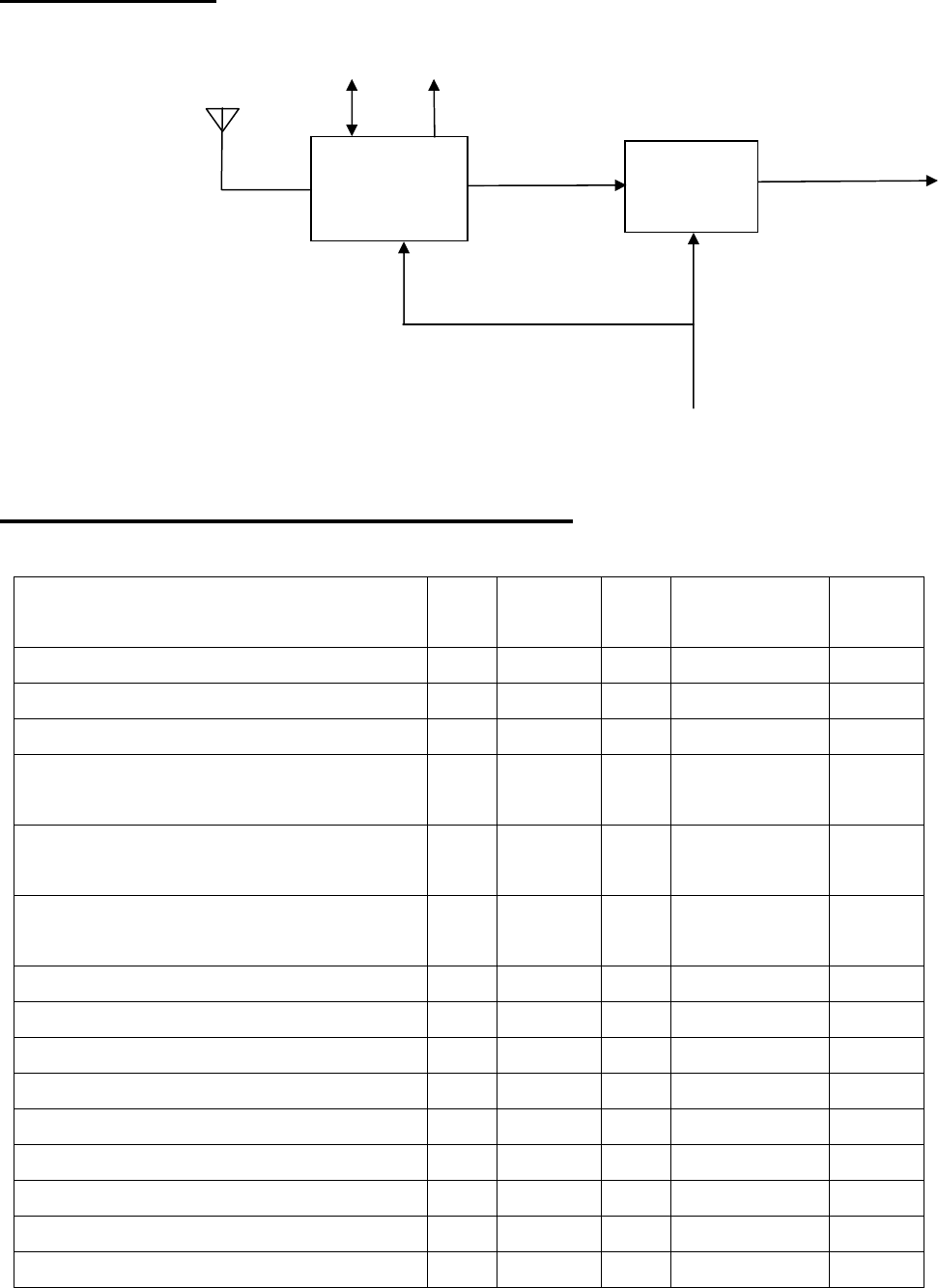
Block Diagram
RF Specification: Temperature=+20℃
Transmitter
Min Typ Max Bluetooth
Specification
Unit
Maximum RF transmit power - 2 - -6 to +4 dBm
RF power control range 3 4.5 5.5 ≥16 dB
20dB bandwidth for modulated carrier - 900 - ≤1000 kHz
Adjacent channel transmit power F = F0 ±
2MHz
- -32 - ≤-20 dBm
Adjacent channel transmit power F = F0 ±
3MHz
- -38 - ≤-40 dBm
Adjacent channel transmit power F = F0 ±
> 3MHz
- -65 - ≤-40 dBm
∆f1avg Maximum Modulation - 165 - 140<f1avg<175 kHz
∆f2max Minimum Modulation - 140 - 115 kHz
∆f1avg/∆f2avg - 0.9 - ≥0.80
Initial carrier frequency tolerance - ±15 - ±75 kHz
Drift Rate ±7 ≤20 kHz/50μ
Drift (single slot packet) - ±10 - ≤25 kHz
Drift (five slot packet) - ±10 - ≤40 kHz
2nd Harmonic Content - -27 - ≤-30 dBm
3rd Harmonic Content - -26 - ≤-30 dBm
BTM645 TPA6112
Differntial
Analog Audio
Single End
Analog Audio
3.3V
LED Control
PIO

Receiver
Freque
ncy
(GHz)
Min
Typ
Max
Bluetooth
Specificatio
n
Unit
2.402 - -86 -
2.441 - -90 -
Sensitivity at 0.1% BER
for all packet types
2.480 - -90 -
≤-70
dBm
Maximum received signal at 0.1% BER - >-10 ≥-20
dBm
C/I co-channel - 5 - ≤11 dB
Adjacent channel selectivity C/I
F = F0 + 1MHz
- -5 - ≤0
dB
Adjacent channel selectivity C/I
F = F0 - 1MHz
- -2 - ≤0 dB
Adjacent channel selectivity C/I
F = F0 + 2MHz
- -40 - ≤-30 dB
Adjacent channel selectivity C/I
F = F0 - 2MHz
- -32 - ≤-20 dB
Adjacent channel selectivity C/I
F = F0 + 3MHz
- -47 - ≤-40 dB
Adjacent channel selectivity C/I
F = F0 - 5MHz
- -45 - ≤-40 dB
Adjacent channel selectivity C/I
F = FImage
- -29 - ≤-9 dB
Maximum level of intermodulation
interferers
- -15 - ≥-39 dBm
Spurious output level - -155 - dBm/
Hz

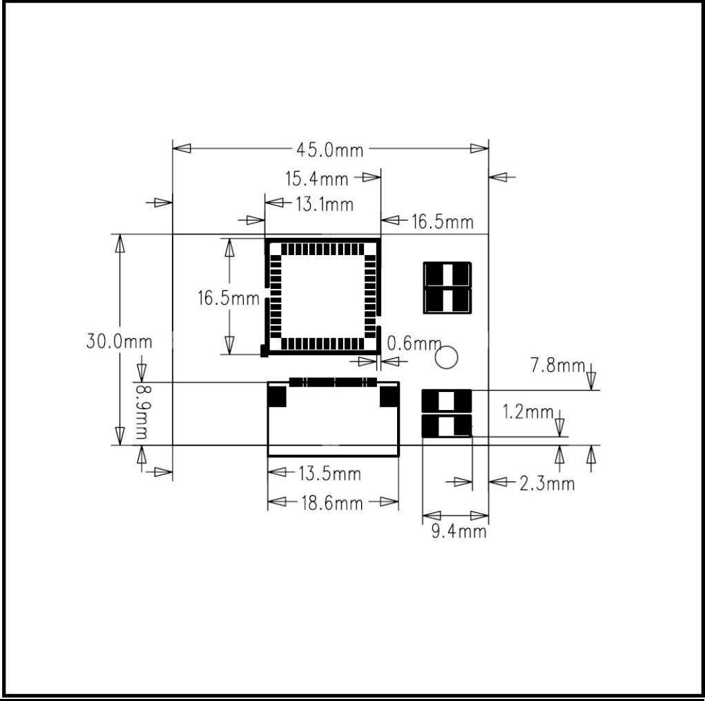
B6Z-400 Pin Functions
No. Pin Name Pin Type Pin Description
1 NC -- --
2 SPKR_R Analogue Speaker output positive, right
3 SPKR_L Analogue Speaker output negative, left
4 AGND Analogue Analog Ground
5 PIO8 Digital I/O PIO8 of BTM645
6. PIO9 Digital Input PIO9 of BTM645, (Reset Pairing List)
7. PIO20 Digital Input PIO20 of BTM645, (Next Track)
8. PIO21 Digital Input PIO21 of BTM645, (Volume +)
9. PIO19 Digital Input PIO19 of BTM645, (Previous Track)
10. PIO18 Digital Input PIO18 of BTM645, (Play/Pause)
11. PIO7 Digital Input PIO7 of BTM645, (Volume -)
12. PIO6 Digital Output PIO6 of BTM645, (Amplifier Enable Control)
13. PIO17 Digital Output PIO17 of BTM645, (To Enter Pairing mode)
14 GND System Ground System Ground
15 VBAT_3V3 Power Input The main Power supply to B6Z-400
16. VREG_ENABLE Analogue Regulator enable input
17. SPI_MISO Bi-directional SPI_MOSI:SPI data input
18. SPI_CLK Bi-directional SPI_CLK:SPI clock input
19. SPI_MISO Bi-directional SPI_MISO:SPI data output
20. SPI_CSB Bi-directional SPI_CSB:SPI Select input
21. LED2 Open drain
output LED Driver
22. LED1 Open drain
output LED Driver
23 LED0 Open drain
output LED Driver
24 RST# Input with
strong pull-up
Active low. Pull low for minimum 5ms to cause a
reset
25. AIO0 Bi-directional Analogue programmable input/output line
Interfaces
Analogue I/O Ports, AIO
B6Z-400 has 1 general-purpose analogue interface pin, AIO[0]. Typically, this connects to a thermistor for
battery pack temperature measurements during charge control.
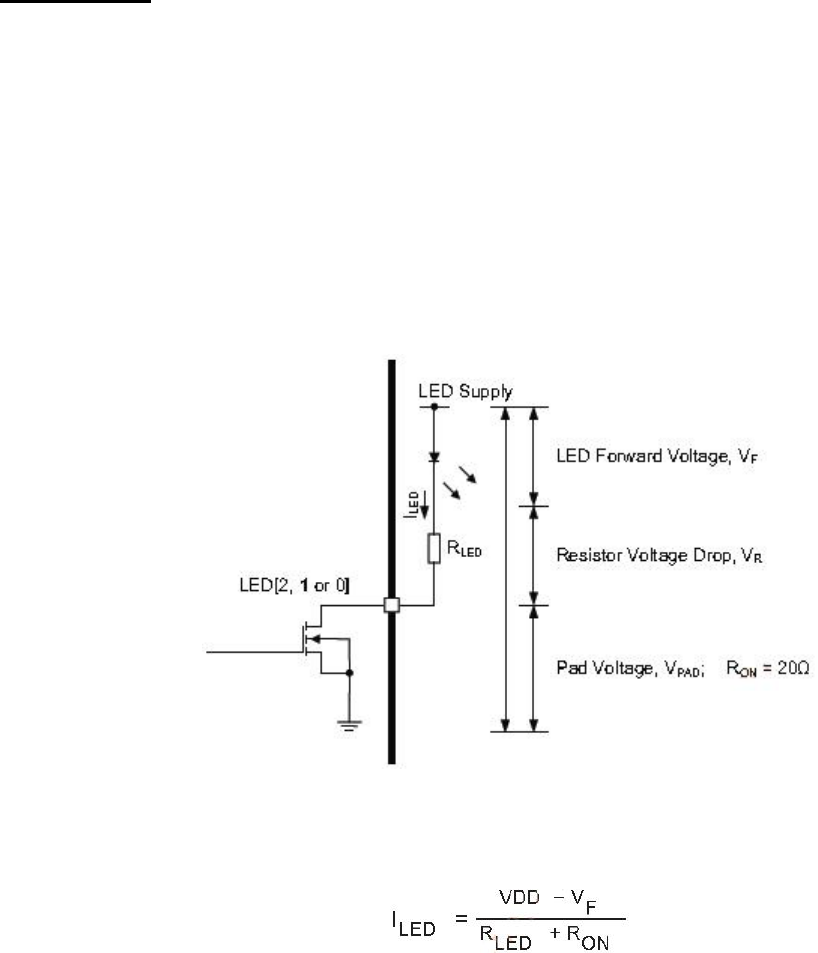
LED Drivers
B6Z-400 includes a 3-pad synchronised PWM LED driver for driving RGB LEDs for producing a wide range
of colours. All LEDs are controlled by firmware.
The terminals are open-drain outputs, so the LED must be connected from a positive supply rail to the pad in series
with a current-limiting resistor.
Figure 2.1: LED Equivalent Circuit
From Figure 2.1 it is possible to derive Equation 2.1 to calculate ILED. If a known value of current is required through
the LED to give a specific luminous intensity, then the value of RLED is calculated.
Equation 2.1: LED Current
For the LED pads to act as resistance, the external series resistor, RLED, needs to be such that the voltage drop
across it, VR, keeps VPAD below 0.5V. Equation 2.2 also applies.
VDD = VF + VR + VPAD
Equation 2.2: LED PAD Voltage
Note:
The LED current adds to the overall current. Conservative LED selection extends battery life.
Reset, RST#
B6Z-400 is reset from several sources:
■ RST# pin
■ Power-on reset
■ USB charger attach reset

■ Software configured watchdog timer
The RST# pin is an active low reset and is internally filtered using the internal low frequency clock oscillator. Rayson
recommends applying RST# for a period >5ms.
At reset the digital I/O pins are set to inputs for bidirectional pins and outputs are set to tristate.
Digital Pin States on Reset
Table 3.3.1 shows the pin states of B6Z-400 on reset.
Pin Name / Group I/O Type Full Chip Reset
USB_DP Digital bidirectional N/A
USB_DN Digital bidirectional N/A
PIO[0] Digital bidirectional PUS
PIO[1] Digital bidirectional PUS
PIO[2] Digital bidirectional PDW
PIO[3] Digital bidirectional PDW
PIO[4] Digital bidirectional PDW
PIO[5] Digital bidirectional PDW
PIO[6] Digital bidirectional PDS
PIO[7] Digital bidirectional PDS
PIO[8] Digital bidirectional PUS
PIO[9] Digital bidirectional PDS
PIO[16] Digital bidirectional PUS
PIO[17] Digital bidirectional PDS
PIO[18] Digital bidirectional PDW
PIO[19] Digital bidirectional PDW
PIO[20] Digital bidirectional PDW
PIO[21] Digital bidirectional PDW
Table 3.3.1: Pin States on Reset
Note:
PUS = Strong pull-up
PDS = Strong pull-down
PUW = Weak pull-up
PDW = Weak pull-down
FederalCommunicationsCommission(FCC)Statement
15.21
Youarecautionedthatchangesormodificationsnotexpresslyapprovedbythepartresponsiblefor
compliancecouldvoidtheuser’sauthoritytooperatetheequipment.
15.105(b)
ThisequipmenthasbeentestedandfoundtocomplywiththelimitsforaClassBdigitaldevice,
pursuanttopart15oftheFCCrules.Theselimitsaredesignedtoprovidereasonableprotection
againstharmfulinterferenceinaresidentialinstallation.Thisequipmentgenerates,usesandcan
radiateradiofrequencyenergyand,ifnotinstalledandusedinaccordancewiththeinstructions,
maycauseharmfulinterferencetoradiocommunications.However,thereisnoguaranteethat
interferencewillnotoccurinaparticularinstallation.Ifthisequipmentdoescauseharmful
interferencetoradioortelevisionreception,whichcanbedeterminedbyturningtheequipmentoff
andon,theuserisencouragedtotrytocorrecttheinterferencebyoneormoreofthefollowing
measures:
‐Reorientorrelocatethereceivingantenna.
‐Increasetheseparationbetweentheequipmentandreceiver.
‐Connecttheequipmentintoanoutletonacircuitdifferentfromthattowhichthereceiveris
connected.
‐Consultthedealeroranexperiencedradio/TVtechnicianforhelp.
ThisdevicecomplieswithPart15oftheFCCRules.Operationissubjecttothefollowingtwo
conditions:
1)thisdevicemaynotcauseharmfulinterference,and
2)thisdevicemustacceptanyinterferencereceived,includinginterferencethatmaycause
undesiredoperationofthedevice.
FCCRFRadiationExposureStatement:
ThisequipmentcomplieswithFCCradiationexposurelimitssetforthforanuncontrolled
environment.EndusersmustfollowthespecificoperatinginstructionsforsatisfyingRFexposure
compliance.Thistransmittermustnotbeco‐locatedoroperatinginconjunctionwithanyother
antennaortransmitter.
Note:Theendproductshallhasthewords“ContainsTransmitterModuleFCCID:PU5B6Z400”