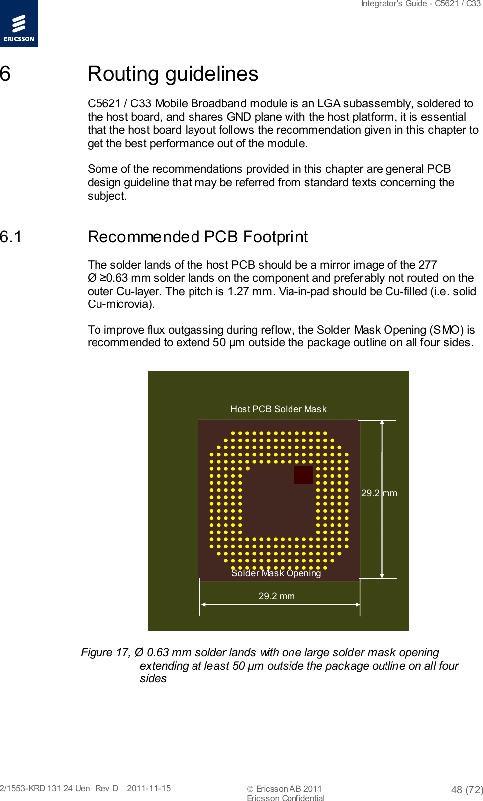
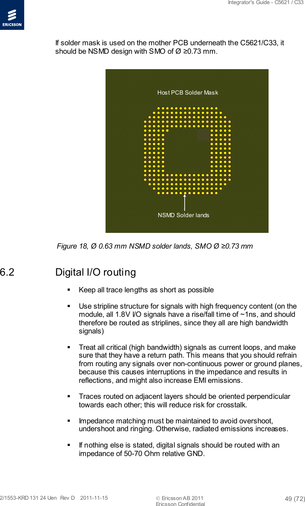
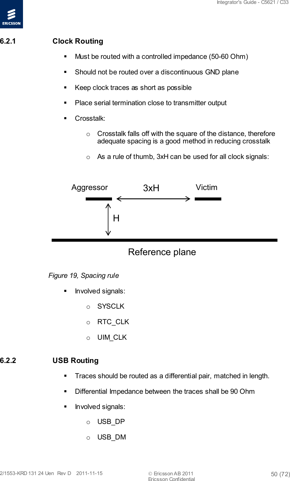
Wistron TP00043AEF 10.1 inch Tablet with 802.11 abgn 1x1 + BT 4.0 User Manual Integrator s Guide C5621 C33
Wistron Corporation 10.1 inch Tablet with 802.11 abgn 1x1 + BT 4.0 Integrator s Guide C5621 C33
Wistron >
Contents
- 1. users guide
- 2. User guide
- 3. user guide
- 4. Integrators guide
- 5. Regulatory notice
Integrators guide
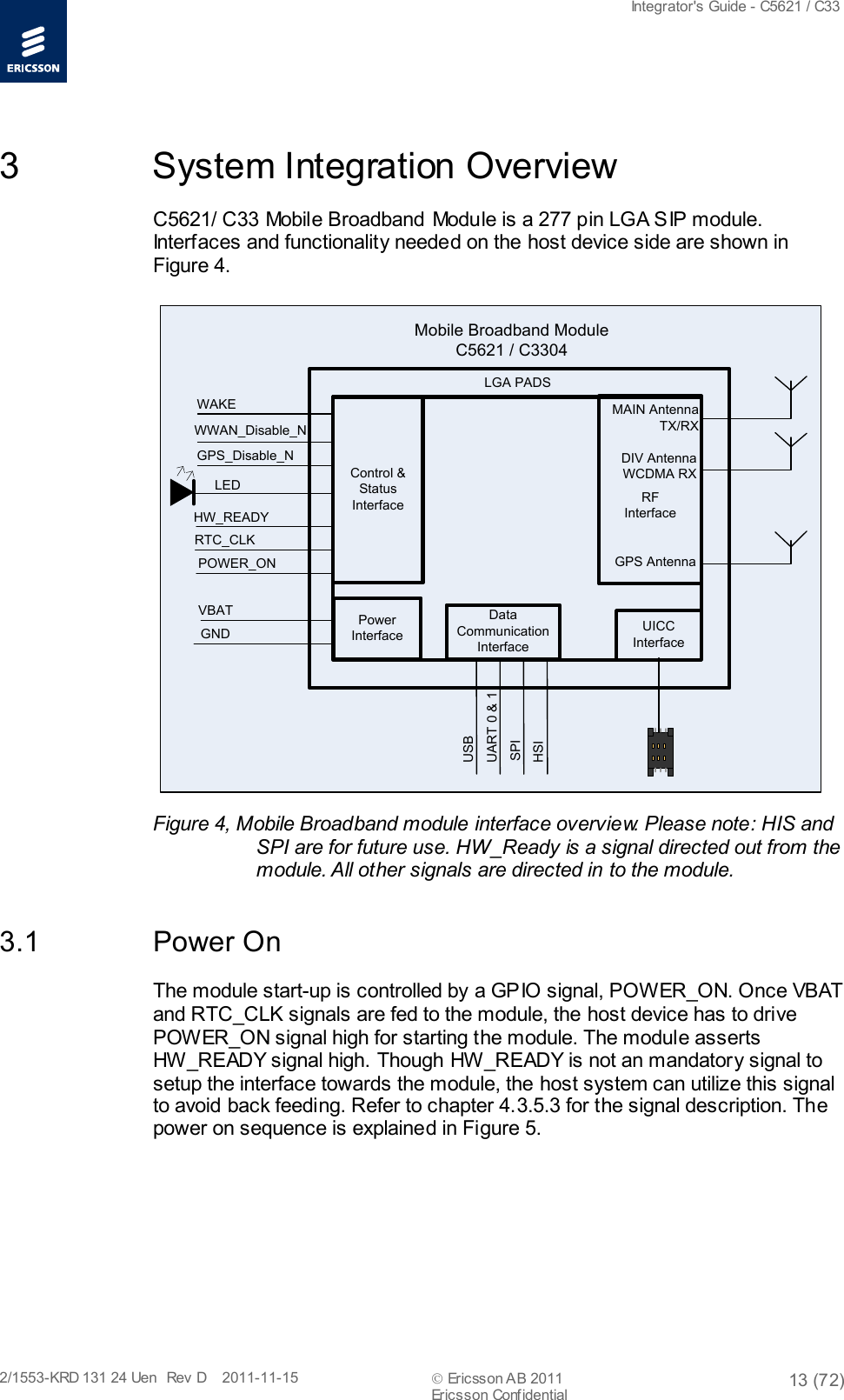
![Integrator's Guide - C5621 / C33 2/1553-KRD 131 24 Uen Rev D 2011-11-15 Ericsson AB 2011 6 (72) Ericsson Confidential 1 Introduction Ericsson’s C5621/C33 Mobile Broadband Module is a 277 pin LGA subassembly, which enables end users to have mobile access to the internet or corporate network with flexibility and high speed, including ‘always online’ capability. It supports data services HSPA Evolution, HSPA, UMTS, EDGE, GPRS, and SMS. The C5621 module also has an integrated GPS receiver, which can be used by positioning applications. The Ericsson Mobile Broadband Module is a solution designed as an add-in option for various host devices such as netbooks, tablets, Personal Navigation Devices (PND), e-Readers, handheld gaming devices, cameras and other consumer devices. The integration of HSI and SPI are not covered in this document. However, they will be covered in future revisions. Product introduction and general information can be found in the Technical Description and User Guide for the mobile broadband module, see [1]. 1.1 Target Users The Ericsson Mobile Broadband Modules are designed for the embedded community for integration into any host device. Target focus is mainstream PC-OEM businesses making slim tablet devices, Personal Navigation Devices (PND), e-Readers and other consumer devices. 1.2 Prerequisites Integration of the Ericsson Mobile Broadband Module should be performed at facilities under host device management. The necessary integration instruction, driver software and user documentation will be provided. No special prerequisite knowledge is necessary. In general, it is recommended to follow the guidelines presented by GSMA for the integration of 3G WWAN modules into notebook computers, see 3G in Notebooks Guidelines [2].](https://usermanual.wiki/Wistron/TP00043AEF.Integrators-guide/User-Guide-1834315-Page-6.png)
![Integrator's Guide - C5621 / C33 2/1553-KRD 131 24 Uen Rev D 2011-11-15 Ericsson AB 2011 8 (72) Ericsson Confidential HostPower OnMobile Broadband ModulePower OnGetDescriptorsSoft DetachVID, PID model and vendor nameContinue Start-upSet ConfigurationUSB_D+ Quick EnumerationUSB_D+ Full Enumeration Figure 1, USB quick-enumeration process 2.2 Always On The Mobile Broadband Module behavior when the host enters Sleep (ACPI S3) or Hibernate (ACPI S4) is configurable by registry key settings. The WMCore service can command the module to either shut down or stay registered to the network - “Alwa ys On”. When the Always On setting is enabled, the module shall be kept powered-on while the host device goes into sleep/hibernate. When the Always On setting is disabled, the module power supply shall be turned off when host device enters Sleep. If “ Always On” is enabled, the WWAN LED and WWAN disable functionality shall also be supported by the host device when in S3. This requirement is to ensure that the WWAN LED indication is available even if the host device is in Sleep state. For implementations that do not use the WMCore service, such as Linux or 3rd party connection managers, the host device software is required to handle the Always On functionality if implemented. It is also possible to configure the Mobile Broadband Module to automatically enable the radio and register to the network without interaction with the host device software. The module checks this configuration at each start-up and changes the radio state accordingly. Please refer to ME Radio Policy in the AT command manual [4].](https://usermanual.wiki/Wistron/TP00043AEF.Integrators-guide/User-Guide-1834315-Page-8.png)
![Integrator's Guide - C5621 / C33 2/1553-KRD 131 24 Uen Rev D 2011-11-15 Ericsson AB 2011 9 (72) Ericsson Confidential 2.3 Wake on Wireless The module supports Wake on Wireless (WoW) functionality, i.e. wake the host from sleep states. The WoW feature requires the host device to have the Always On feature enabled. The WoW trigger-rules can be set by AT commands. The WoW functionality can be configured to use the USB interface or WAKE_N signal to trigger a wake-up signal in order to wake up the host. Table 1 WoW support M ode l Interface Host State (ACPI) C5621 / C33 USB, WAKE_N signal Sleep (S3), Hibernate (S4) and Off (S5). The module can be configured to wake the host when an SMS, starting with a predefined text string (payload) and/or with a predefined originating address, is received by the module. When an SMS, which corresponds to the above criteria, is received an unsolicited AT response is generated. The wake event is signaled using the USB and the normal USB wakeup procedure is triggered. Additionally it is possible to configure out of band wakeup signaling using the WAKE_N signal. In addition to wakeup triggered by SMS, the module can be configured to wake the host when other predefined events occur, which generate unsolicited AT responses. Examples are changes in network status, reception of any SMS and SMS memory full. If the wake up was triggered by an SMS, the payload can be fetched using the SDK or AT commands [9] when the host has resumed from its sleep state. For further details see [15]. 2.4 Idle Mode Power Management The Mobile Broadband Module supports features to minimize power consumption when in idle mode. Based on the ongoing activities in the module, the module is able to remove or decrease power in various parts of the platform.](https://usermanual.wiki/Wistron/TP00043AEF.Integrators-guide/User-Guide-1834315-Page-9.png)
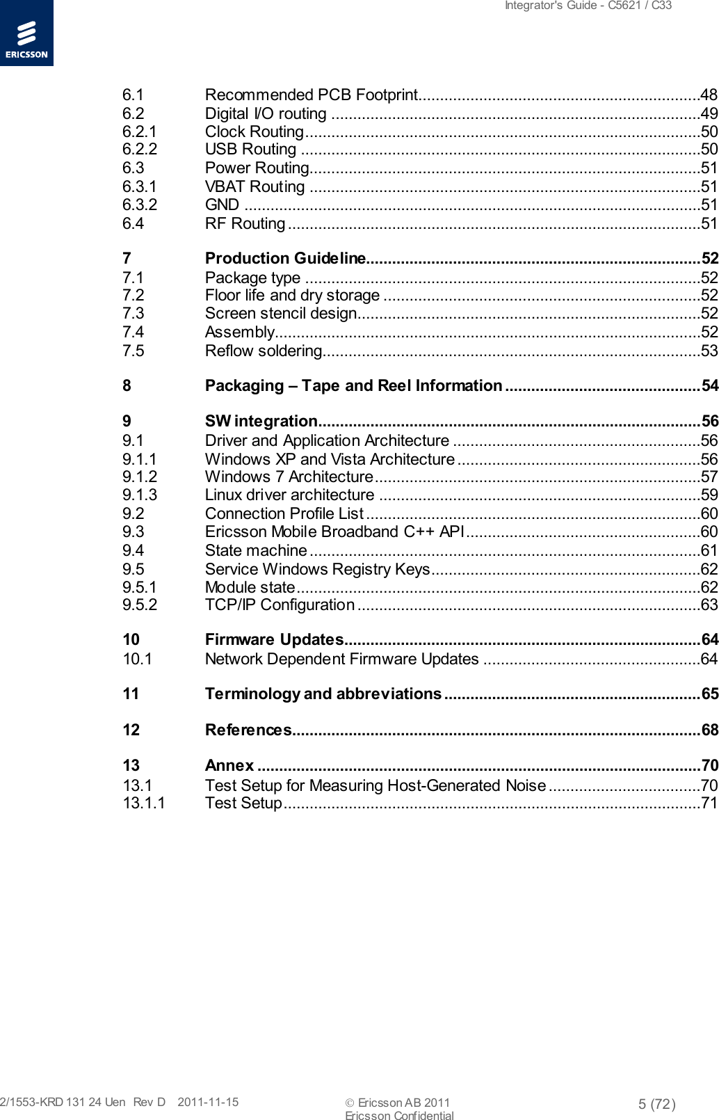
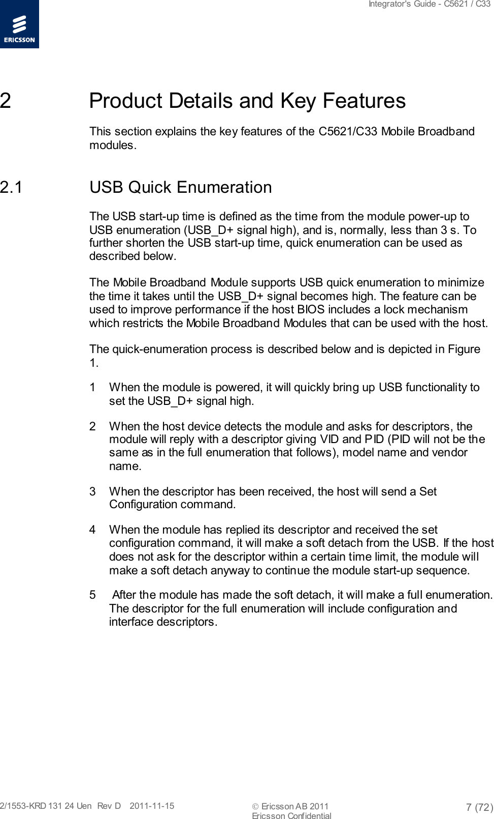
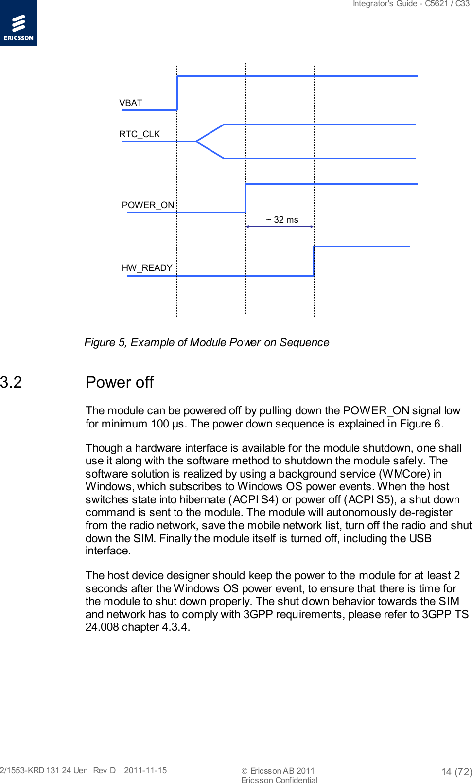
![Integrator's Guide - C5621 / C33 2/1553-KRD 131 24 Uen Rev D 2011-11-15 Ericsson AB 2011 11 (72) Ericsson Confidential The module sends a ‘Signalling Connection Release Indication’ Cause to the network. The UTRAN (network) upon reception of this IE may decide to trigger an RRC State transition to a more battery efficient state, ultimately IDLE. Fast Dormancy is triggered and is steered from the host and it’s a feature available in 3GPP release 8. Note: The fast dormancy support in C5621 has one of the timers (T323) set to a default value of 60 seconds. 2.5 Over-temperature protection To protect the Mobile Broadband Module hardware from over-heating, and to ensure radio performance and component life length, the module supports over-temperature protection. The over-temperature protection function consists of three parts: • Over-temperature signaling • GPS thermal throttling • PA thermal throttling 2.5.1 Over-temperature signaling This function reports to the host SW, e.g. connection manager software, when the temperature passes through some configurable temperature threshold; refer to the SDK [5] and the AT Command Manual [4] for details. 2.5.2 GPS Thermal Throttling The GPS Thermal Throttling function limits the GPS functionality according to module temperature. This is done to prioritize module functionality in higher temperatures. GPS will automatically turn off when temperature exceeds Threshold A, see Figure 2. Any changes in the GPS status depending on this function is reported, unsolicited, to the host software; see the SDK [5] and the AT Command Manual [4] for details.](https://usermanual.wiki/Wistron/TP00043AEF.Integrators-guide/User-Guide-1834315-Page-11.png)
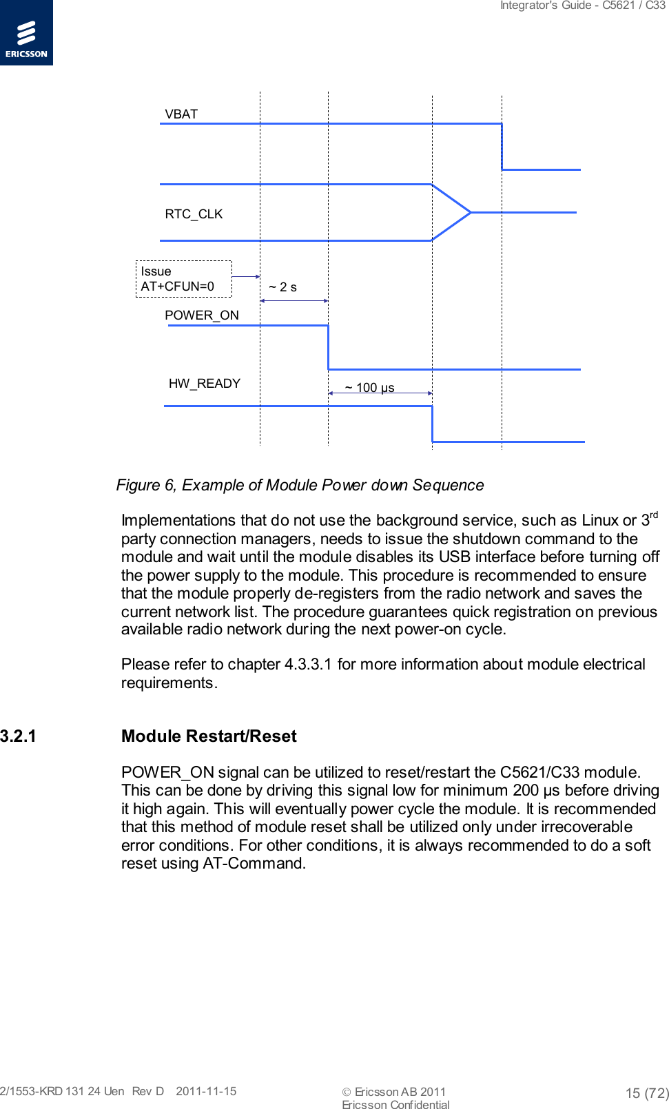
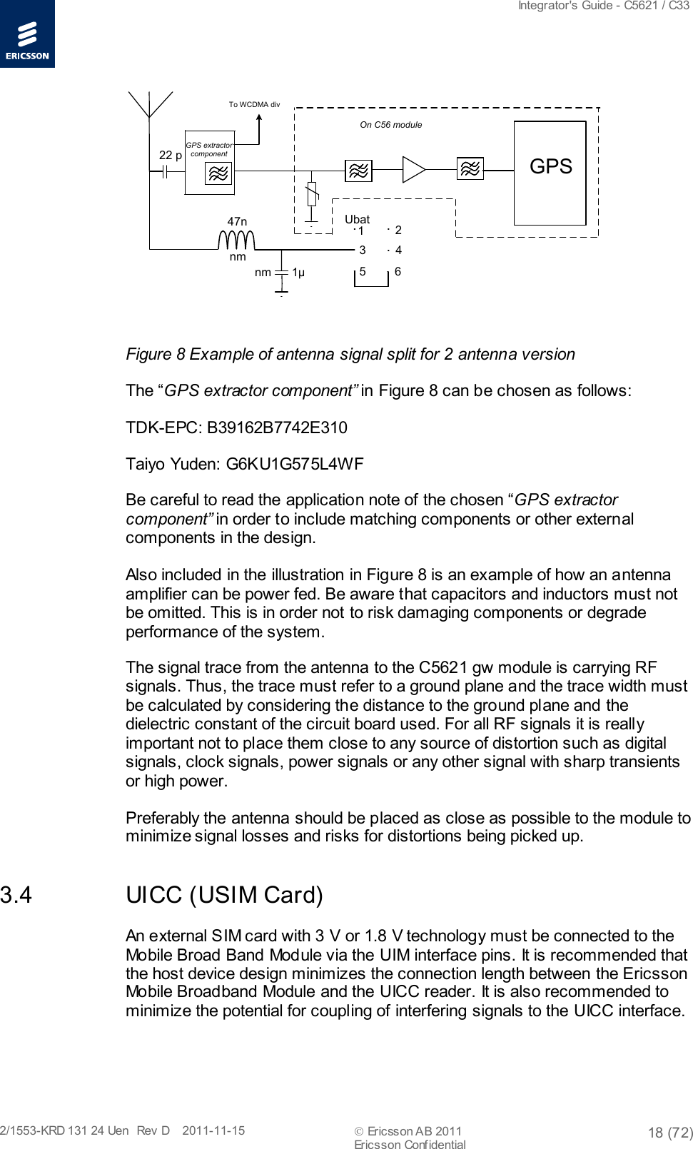
![Integrator's Guide - C5621 / C33 2/1553-KRD 131 24 Uen Rev D 2011-11-15 Ericsson AB 2011 16 (72) Ericsson Confidential ≥200 μsHW_READYPOWER_ONRTC_CLKVBATModule Reset Cycle Figure 7, Example of Module Reset Sequence 3.3 GPS Interface The Mobile Broadband Module supports different kinds of assisted GPS features, which put requirements on SW to be installed on the host side and in some use cases also agreements to be signed by the integrator. 3.3.1 Antenna Recommendations The GPS performance when integrated in a host device is dependent on antenna efficiency (including cable loss), antenna pattern/polarization and host-generated noise. The internal noise can be generated from DC/DC converter, LCD, CPU, hard drives etc and other co-existing radio transceivers (e.g. WLAN and Bluetooth). To achieve good performance the host-generated noise level should be less than -116.5 dBm/MHz in 1525.42 ± 1 MHz band. The noise level is not possible to measure with conventional instruments. However, there is a way to estimate the noise added by the host platform using an Over-The-Air (OTA) measurement setup. The test setup is described in chapter 13.1. General recommendation for designing 3G, 2G and GPS antenna is stated in the ‘Antenna Performance Guideline’ document [10].](https://usermanual.wiki/Wistron/TP00043AEF.Integrators-guide/User-Guide-1834315-Page-16.png)
![Integrator's Guide - C5621 / C33 2/1553-KRD 131 24 Uen Rev D 2011-11-15 Ericsson AB 2011 19 (72) Ericsson Confidential Note: The UICC design (UICC reader, signal strength and integrity), is part of the 3GPP testing on system level. Note: UICC electrical requirements are not guaranteed by the module in the event of UICC Hot swap. Host device design is required to choose a UICC socket which offers such protection. Note: This is a software-based solution. The SIM_OFF signal is not used. 3.4.1 UICC Hot Swap The Mobile Broadband module will autonomously detect and reset its internal logic to handle a UICC hot swap. The module can be configured to send an unsolicited AT response when a UICC removal event is registered. When a UICC detection event is registered, the host will be alerted by an unsolicited response before the module is automatically restarted. The WMCore service handles this logic and will issue UICC event notifications on the C++ API [5]. The host must be prepared for an automatic module restart when a UICC detection event is registered. For implementations that do not use the WMCore service, such as Linux or 3rd party connection managers, the host device software is required to handle the UICC hot swap functionality, if implemented. 3.5 Electrostatic Discharge (ESD) Precautions The Ericsson Mobile Broadband Module is Electrostatic Discharge (ESD) protected. However, it is recommended that integrators follow electronic device handling precautions when working with any electronic device system to prevent damage to the host or the radio device. When the Ericsson Mobile Broadband Module is mounted in the host, it is the responsibility of the integrator to ensure that static discharge protection is designed in to the host product. If exposed, the antenna and UICC interfaces are vulnerable contact points for ESD.](https://usermanual.wiki/Wistron/TP00043AEF.Integrators-guide/User-Guide-1834315-Page-19.png)
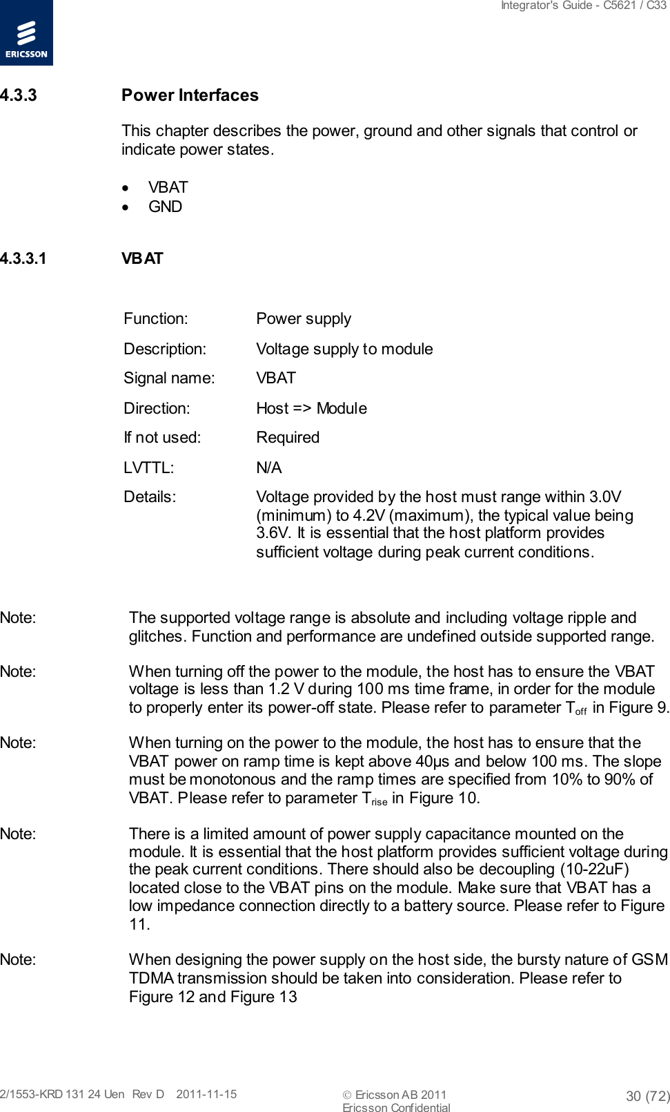
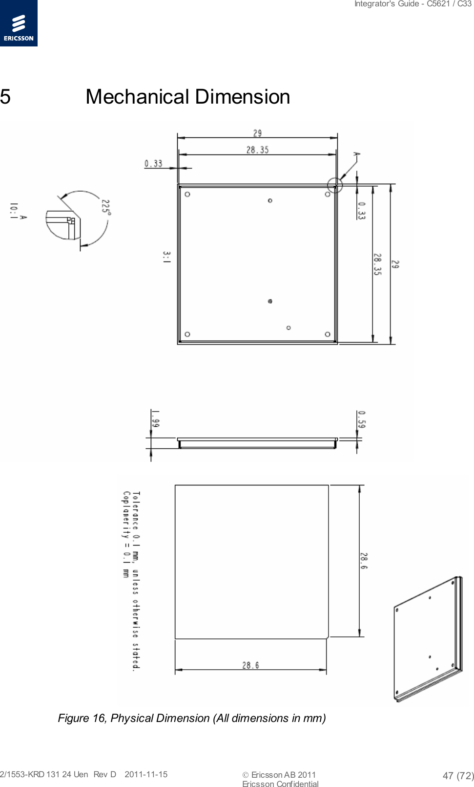
![Integrator's Guide - C5621 / C33 2/1553-KRD 131 24 Uen Rev D 2011-11-15 Ericsson AB 2011 20 (72) Ericsson Confidential 4 Electrical Integration This chapter describes the electrical interface between the Ericsson Mobile Broadband Module and the host device. A summary of the function of each signal is provided, together with any additional relevant information. Signals are described from the perspective of the Ericsson Mobile Broadband Module. Consequently, signals described as ‘Input’ are input signals to the module, driven by the host [Host ⇒ Module]. Likewise, signals described as ‘Output’ are driven by the module into the host [Module ⇒ Host]. Bi-directional signal flow (I/O) is indicated by a double-headed arrow [Module ⇔ Host]. In cases like UICC interface, which utilizes the host circuitry to interface to the module, it will be indicated as an interface between the module and the respective component, like [Module ⇒ UICC]. Apart from the module soldering process, the system radio performance depends also on host system design, host device noise, antenna design and performance etc. The host antenna system design is very important for total radio performance. For minimal system 3G performance recommendations see [2]. Note that the operators may have stricter radio performance requirements than stated in [1]. This equipment complies with FCC radiation exposure limits set forth for an uncontrolled environment if the equipment is installed and operated with minimum distance of 20 cm between the radiator and your body. Depending on host design and antenna location there are requirements on human body exposure to RF emissions, please refer to [11] and [12] for more information. The transmitter must not be co-located or operating in conjunction with any other antenna or transmitter. 4.1 Physical size Width: 29 (±0.1) mm Length: 29 (±0.1) mm Height: < 1.99 (±0.1) mm](https://usermanual.wiki/Wistron/TP00043AEF.Integrators-guide/User-Guide-1834315-Page-20.png)
![Integrator's Guide - C5621 / C33 2/1553-KRD 131 24 Uen Rev D 2011-11-15 Ericsson AB 2011 33 (72) Ericsson Confidential Direction: N/A If not used: Required LVTTL: N/A Details: Return path for all currents and ground reference. 4.3.4 Data communication interfaces 4.3.4.1 USB 2.0 Function: USB2.0 data communication port Description: USB transmit and receive port for data communication between module and host Signal name: USB_DP USB_DM Direction: Module host If not used: Required LVTTL: N/A Details: The module USB interface is designed to the High Speed USB specifications; see Universal Serial Bus Specification 2.0 [3]. Power to the USB interface is provided by VBAT input from the host. The USB start-up time, i.e. from module startup to D+ high, is less than 3 s. The module has support for quick enumeration which allows for even shorter BIOS detection times, please see chapter 2.1 Note: Ericsson strongly recommends that the USB is connected directly to the root HUB, which is not shared with other USB devices. This ensures that the module USB selective suspend function is not limited by other devices connected to the same HUB. Note: To achieve full throughput performance, the USB host controller should adhere to USB2.0 specification and be configured for High Speed Mode.](https://usermanual.wiki/Wistron/TP00043AEF.Integrators-guide/User-Guide-1834315-Page-33.png)
![Integrator's Guide - C5621 / C33 2/1553-KRD 131 24 Uen Rev D 2011-11-15 Ericsson AB 2011 34 (72) Ericsson Confidential 4.3.5 Debug Interface UART 0 & 1 signals are used for debugging purpose, when USB interface is disconnected or suspended. Signals shall be routed to test pads or to a test connector. All signals shall be placed on the same side of the board, for the ease of accessibility. UART0 CTS & RTS signals can be left as ‘NC’ as they are not utilized for debugging purpose. Added to this, TEST_PIN (Pin V2) shall be placed along with these UART signals for debugging. There is cable detection functionality. Thus, if the signal goes low on these lines then the module will not go to suspend. It is rec ommended that the mentioned signals are routed to test pads or test connector since Ericsson will use them for claims purposes. Along with the UART signals, USB_DN, USB_DP and RTC_CLK signals from the module shall be terminated on test pads. These signals shall be used for debugging the module in the stand-alone mode. The recommendations for stand-alone mode are described further in this section. 4.3.5.1 UART0 Function: UART0 data communication port (for debugging) Description: UART data communication port with flow control Signal name: UART0_TX UART0_RX UART0_ RTS UART0_ CTS Direction: Module host If not used: Leave open LVTTL: 1.8V Details: 115200 baud, 8 data bit, 1 stop bit, no parity, flow control. Electrical specification and signaling levels according to [13]. This port is used for debugging purpose. 4.3.5.2 UART1 Function: UART1 data communication port (for debugging) Description: UART data communication port without flow control Signal name: UART1_TX UART1_RX Direction: Module host](https://usermanual.wiki/Wistron/TP00043AEF.Integrators-guide/User-Guide-1834315-Page-34.png)
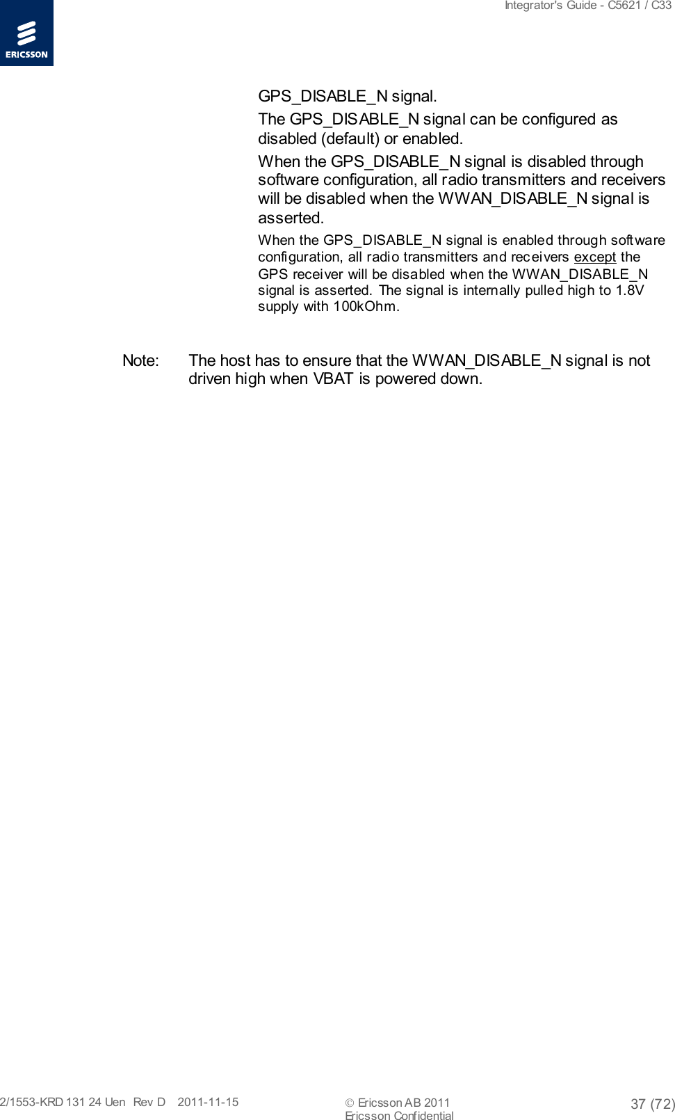
![Integrator's Guide - C5621 / C33 2/1553-KRD 131 24 Uen Rev D 2011-11-15 Ericsson AB 2011 35 (72) Ericsson Confidential If not used: Leave open LVTTL: 1.8V Details: 115200 baud, 8 data bit, 1 stop bit, no parity, no flow control. Electrical specification and signaling levels according to [13]. This port is used for debugging purpose. 4.3.5.3 Interface for Stand-alone Debug Mode Ericsson recommends the device integrators to provide an option to start up the module in ‘stand alone’ debug mode. This interface will primarily be used for debugging during the R&D phase of the device integrators and by Ericsson personnel during claims process. The intention of defining this interface is to test the C5621/C33 module stand-alone, if any issues in the system functionality or performance is reported. This will help to isolate the root cause of the issue. To start up the module in stand-alone, the following recommendations are to be considered: • There shall be possibility to power-up the module in the stand-alone mode, preferably from an external power source (VBAT), bypassing the host power-on control logic. The corresponding reference GND shall also be provided on a test pad. • RTC_CLK (32.768kHz) shall be available to start up the module in this mode. Terminating RTC_CLK to a test pad enables the possibility to connect this signal to an external clock source. • A default pull-up option for POWER_ON signal enables the module to power-up even when this signal is isolated from the host control logic. • Possibility to connect USB traces to an external host – by soldering cable to the test pads or by routing USB traces to a test USB connector. • Series zero ohm resistors are to be provided on USB_DP, USB_DN, POWER_ON and RTC_CLK signals so that these signals can be isolated to the external test pads in the stand-alone mode. • UICC interface on the host PCB shall be available, by default, so that the module is able to communicate with the SIM. The mentioned signals along with the UART signals and TEST_PIN shall be placed in the same order as indicated in Figure 14, - pin 1 being referred as UART0_RX.](https://usermanual.wiki/Wistron/TP00043AEF.Integrators-guide/User-Guide-1834315-Page-35.png)
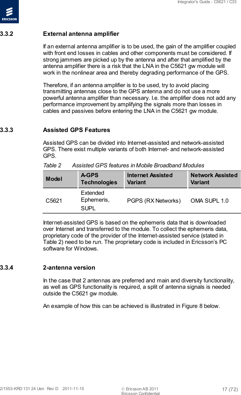
![Integrator's Guide - C5621 / C33 2/1553-KRD 131 24 Uen Rev D 2011-11-15 Ericsson AB 2011 42 (72) Ericsson Confidential LVTTL: 1.8V Details: The clock presented on the SYSCLK signal is referenced to the WWAN system clock. 4.3.7 UICC Interface The UICC interfaces consist of the following signals: • UIM Power • UIM Data • UIM Clock • UIM Reset • UIM SIMOFF The picture below illustrates the UICC (SIM) interface. Note: The UICC interface should be ESD protected on the host side. 10kOhmUIM_PWRUIM_CLKUIM_RSTUIM_DATALGA PADSLDO1.8/3V SIM Interface1µFPlace ESD protectionclose to SIM card holderModule Host Device Figure 15, UICC interface 4.3.7.1 UIM _PWR Function: UIM Power Description: 1.8 V or 3 V power supply to the UICC Signal Name: UIM_PW R [Module⇒UICC] If not used: Required](https://usermanual.wiki/Wistron/TP00043AEF.Integrators-guide/User-Guide-1834315-Page-42.png)
![Integrator's Guide - C5621 / C33 2/1553-KRD 131 24 Uen Rev D 2011-11-15 Ericsson AB 2011 43 (72) Ericsson Confidential LVTTL: N/A Details: The UIM_PWR signal is the Ericsson Mobile Broadband Module power supply to the UICC. The Ericsson Mobile Broadband Module supports UICC of Class B and C. The signal details shall be according to [14]. Note: Only the UICC reader may be connected to UIM_PWR. The UIM_PWR signal should not be fitted with decoupling capacitors in the host design. Table 8, UIM_PWR Electrical Characteristics Parameter Condition Min T ype Max Unit UIM_PW R 1.8 V mode 1.67 1.8 1.98 V 3 V mode 2.8 2.85 2.9 V 4.3.7.2 UIM_DATA Function: UIM Data Description: Single-ended data signal Signal Name: UIM_DAT A [Module⇔UICC] If not used: Required LVTTL: N/A Details: The Ericsson Mobile Broadband Module provides this data signal interface to the host mounted UICC. A 10 kOhm pull-up resistor to UIM_PWR is mounted on the module. The signal details shall be according to [14].](https://usermanual.wiki/Wistron/TP00043AEF.Integrators-guide/User-Guide-1834315-Page-43.png)
![Integrator's Guide - C5621 / C33 2/1553-KRD 131 24 Uen Rev D 2011-11-15 Ericsson AB 2011 44 (72) Ericsson Confidential Table 9, UIM_DATA Electrical Characteristics: Parameter Condition Min T ype Max Unit UIM_DATA Input low level 0.2 x UIM_PW R V Input high level 0.7 x UIM_PW R V Output low level 0 0.3 V Output high level U IM_PW R -0.3 U IM_PW R V 4.3.7.3 UIM_CLK Function: UIM Clock Description: Single-ended clock signal Signal Name: UIM_CLK [Module⇒UICC] If not used: Required LVTTL: N/A Details: The Ericsson Mobile Broadband Module provides this clock signal interface to the host mounted UICC. The signal details shall be according to [14]. Table 10, UIM_CLK Electrical Characteristics Parameter Condition Min T ype Max Unit UIM_CLK 1.8 V mode, low level 0 0.2 V 1.8 V mode, high level 1.6 UIM_PW R V 3 V mode, low level 0 0.35 V 3 V mode, high level 2.4 UIM_PW R V 4.3.7.4 UIM_RST Function: UIM Reset Description: Reset signal to the UICC](https://usermanual.wiki/Wistron/TP00043AEF.Integrators-guide/User-Guide-1834315-Page-44.png)
![Integrator's Guide - C5621 / C33 2/1553-KRD 131 24 Uen Rev D 2011-11-15 Ericsson AB 2011 45 (72) Ericsson Confidential Signal Name: UIM_RST [Module⇒UICC] If not used: Required LVTTL: N/A Details: The Ericsson Mobile Broadband Module provides this reset signal interface to the host mounted UICC. The signal details shall be according to [14]. Table 11, UIM_RST Electrical Characteristics Parameter Condition Min T ype Max Unit UIM_RST 1.8 V mode, low level 0 0.2 V 1.8 V mode, high level 1.6 UIM_PW R V 3 V mode, low level 0 0.35 V 3 V mode, high level 2.4 UIM_PW R V 4.3.7.5 UIM_SIMOFF_N (For Future Use) Function: UICC interface disable Description: Active low UICC interface disable Signal Name: UIM_SIMOFF_N [UICC⇒Module] Table 12, UIM_SIMOFF_N Electrical Characteristics Parameter Condition Min T ype Max Unit UIM_SIMOFF_N 1.8 V mode 1.67 1.8 1.98 V 4.3.8 PCM 0 & 1 Interface The module is hardware prepared to support digital voice interface between the module and the host. PCM 0 & 1 are intended for that purpose. For C5621/C33 module configuration, this interface is not enabled. Hence, the signals corresponding to PCM 0 /1 interface shall be pulled-low or tied to GND. Refer to Table 3 for pin details.](https://usermanual.wiki/Wistron/TP00043AEF.Integrators-guide/User-Guide-1834315-Page-45.png)
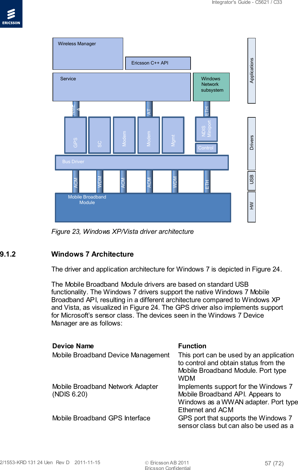
![Integrator's Guide - C5621 / C33 2/1553-KRD 131 24 Uen Rev D 2011-11-15 Ericsson AB 2011 56 (72) Ericsson Confidential 9 SW integration 9.1 Driver and Application Architecture 9.1.1 Windows XP and Vista Architecture The driver and application architecture for XP and Vista is depicted in Figure 23. The drivers are based on standard USB functionality. The Mobile Broadband Module appears as the following devices when examined in Windows Device Manager: Device Name Function Mobile Broadband Device Management This port can be used by an application to control and obtain status from the Mobile Broadband Module. Port type WDM Mobile Broadband Network Adapter (NDIS) NDIS i nterface over which Ethernet communication can be established. Appears to Windows as a network adapter. Port type Ethernet Mobile Broadband GPS Interface GPS COM port which streams out NMEA. Port type ACM SIM Card Reader (SC) PC-Smartcard interface. Port type WDM Wireless Modem Modem device which may be used for legacy Dial-Up Networking connection. Port type ACM. On top of the drivers is an application, WMCore, running as background service. The service is started automatically at Windows startup and can be used to change the state of the Mobile Broadband Module without end-user interaction also prior to Windows login. The WMCore service provides a number of functions to control the module and retrieve information about the module and its states. The functions are accessible through the Ericsson Mobile Broadband C++ API, see [5]. The service is also used by Ericsson’s Wireless Manager.](https://usermanual.wiki/Wistron/TP00043AEF.Integrators-guide/User-Guide-1834315-Page-56.png)
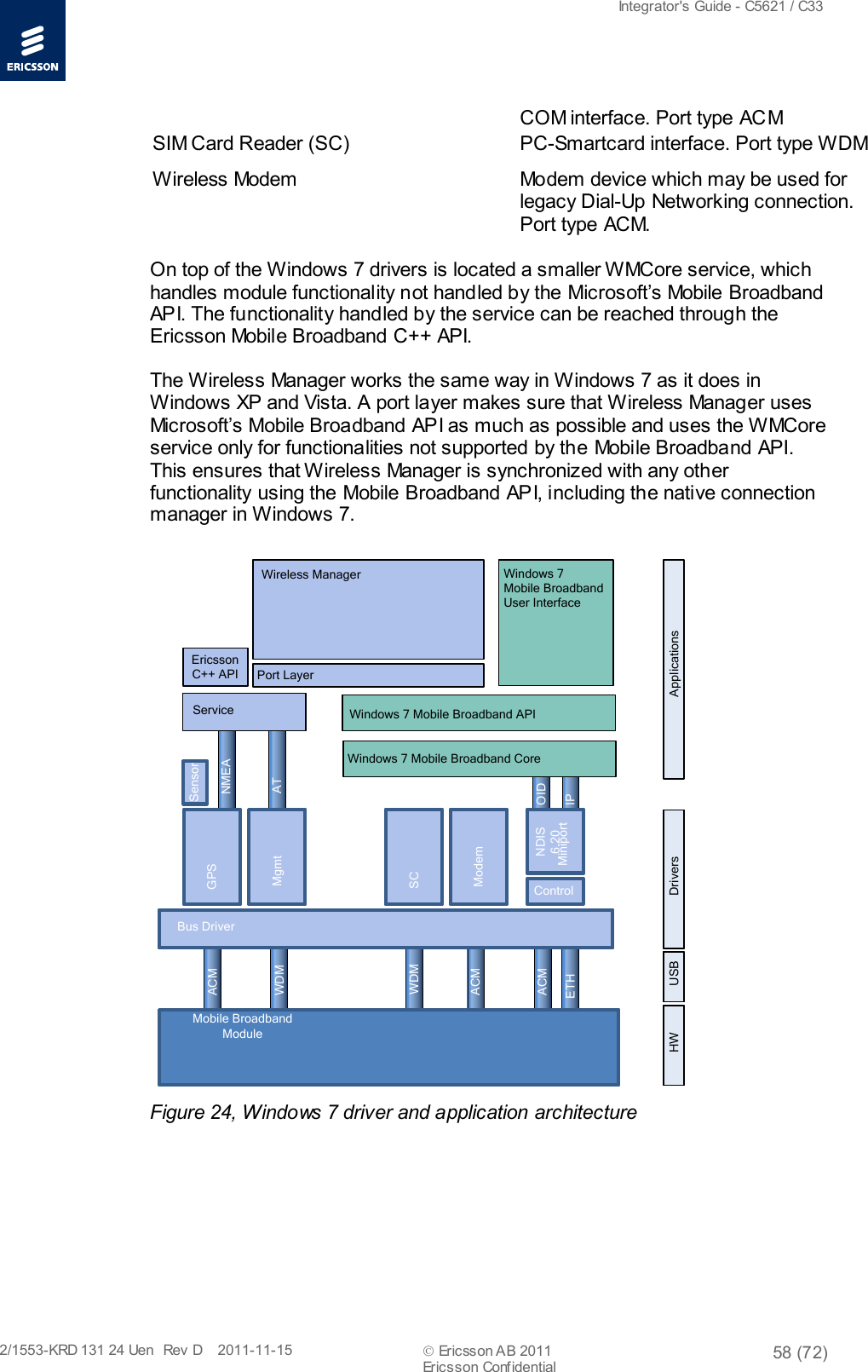
![Integrator's Guide - C5621 / C33 2/1553-KRD 131 24 Uen Rev D 2011-11-15 Ericsson AB 2011 59 (72) Ericsson Confidential 9.1.3 Linux driver architecture Ericsson is a part of the Linux community to continuously improve the support in GNU/Linux for Ericsson Mobile Broadband Modules, please see [7] for more information. The module firmware provides WDM (Wireless Mobile Communications Device Management) interfaces for device management and AC M (Abstract Control Module) interfaces for control and data traffic. The module exposes ACM ports, which can be used for GPS, Connection Manager and SMS. WDM and ACM are both based on CDC (Communication Device Class). Control is handled by AT commands according to the V.25 standard. The network connection uses USBnet architecture as base with support from CDC-NC M. The module supports DUN using PPP on the ACM interface. Note: Kernel modifications may be needed to support customer requested VID/PID customizations, check with your Linux distributor. Network Manager and GPS functionality is provided by user space applications. For more information please refer to [8] Figure 25, Linux driver architecture Host USB HardwareUSB CoreUSBnetACMWDMHardwareKernelLegendGPS Control Kernel-spaceUser-spaceNetwork ManagerModuleCDC-NCM](https://usermanual.wiki/Wistron/TP00043AEF.Integrators-guide/User-Guide-1834315-Page-59.png)
![Integrator's Guide - C5621 / C33 2/1553-KRD 131 24 Uen Rev D 2011-11-15 Ericsson AB 2011 60 (72) Ericsson Confidential 9.2 Connection Profile List In Windows XP and Vista, the WMCore service includes a list with connection profiles which can be used by connection managers when setting up connections. The profile list contains a list of default network operator APN which is automatically selected by the connection manager depending on the detected UICC card. The matching between APN and UICC card is done based on the MCC and MNC (2 or 3 digit). In Windows 7 the list of profiles is part of the WWAN adapter and is accessed and handled through the Windows 7 Mobile Broadband API as specified by Microsoft. Wireless Manager utilizes the profile list in the WMCore service in Windows XP and Vista. In Windows 7, Wireless Manager carries the profile list itself to facilitate updates of the list without requiring a driver update. Updates of the connection profile list can be made by using a Connection Profile Updater, for more information, see [6]. The connection profile updater updates the profile list in WMCore in XP and Vista and the profile list carried by Wireless Manager in Windows 7. 9.3 Ericsson Mobile Broadband C++ API The Ericsson Mobile Broadband C++ API (the C++ API) is part of the Ericsson Mobile Broadband Software Development Kit (SDK), which is available for integration of mobile broadband modules. The C++ API can be used as an extension to the Mobile Broadband API in Windows 7 to access functionality not supported in the Mobile Broadband API. In Windows XP and Vista, the C++ API covers the entire Mobile Broadband API as well as the extensions. The C++ API is backward compatible. The C++ API supports multi-process and multi-thread access. By using the C++ API, application development becomes easier and more efficient since high-level interfaces can be used. The C++ API also leverages on functionality provided by the WMCore service, which includes: • Module state and concurrency handling • Windows Auto-connect and pre-logon connect • Always-on functionality • Automatic state transitions after Sleep(S3) and WWAN disable • GPS configuration • Internet account (APN) configuration](https://usermanual.wiki/Wistron/TP00043AEF.Integrators-guide/User-Guide-1834315-Page-60.png)
![Integrator's Guide - C5621 / C33 2/1553-KRD 131 24 Uen Rev D 2011-11-15 Ericsson AB 2011 62 (72) Ericsson Confidential 9.5 Service Windows Registry Keys The Ericsson WMCore service uses Windows Registry Keys to control the module behavior during OS power-state changes. Windows TCP/IP settings can also be optimized automatically when installing the drivers. When using the Ericsson Mobile Broadband C++ API there is no need to manually control the registry settings, however, integrators opting for using the module without the API could use these. The register settings are used to control the following features: • Always On (OS power event behavior) • Auto connect • Auto radio enable • TCP/IP optimization for WWAN devices. Note: The registry settings are defined within the definition of the WMCore service. The registry settings definition and function can be changed or removed without prior notice. 9.5.1 Module state The following parameters control the module function state during OS power event changes. They are used to synchronize the module state to OS state. Please refer to the AT Command Manual [4] for details on CFUN state. The registry keys are set during the driver and WMCore installation. Search path: [HKEY_L OCA L_MA CHINE\SOFTWARE\WMCore] (32bit installations) [HKEY_LOCAL_MACHINE\S OF TW A RE\Wow6432Node\WMCore] (64bit installations) Table 13 Module state settings Name Type Description LastKnownRadioState REG_DWORD CFUN value to set after boot / reboot. ShutdownCFUN REG_DWORD CFUN value to set before shutdown / reboot. KeepRadioStateDuringSleep REG_DWORD 0: Do not keep current radio state 1: Keep radio state when entering sleep](https://usermanual.wiki/Wistron/TP00043AEF.Integrators-guide/User-Guide-1834315-Page-62.png)
![Integrator's Guide - C5621 / C33 2/1553-KRD 131 24 Uen Rev D 2011-11-15 Ericsson AB 2011 63 (72) Ericsson Confidential Table 14 Connection state settings Name T ype Description AllowAutoConnectAfterSleep REG_DWORD 0: Never autoconnect after sleep, regardless of previous state 1: Allow reconnection, if previously connected. AutoConnectStartup REG_DWORD 0: Do not automatically connect after boot. 1: Automatically connect after boot. DisableAutoConnect REG_DWORD 0: Does nothing 1: Never autoconnect 9.5.2 TCP/IP Configuration As part of installation in Windows XP, the following registry settings are made in order to optimize the throughput for WWAN devices. [HKEY_LOCAL_MACHINE\SYSTEM\Current ControlSet\Services\Tc pip\Paramet ers] Table 15 TCP/IP Optimization Name T ype Value TcpWindowSize REG_DWORD 0x40290 Tcp1323Opts REG_DWORD 0x1 Note: Setting Tcp1323Opts="0x3" and thus enabling Timestamp might help in some cases where there is increased packet loss. However, generally better throughput is achieved with Tcp1323Opts="0x1", since Timestamps add 12 bytes to the header of each IP packet.](https://usermanual.wiki/Wistron/TP00043AEF.Integrators-guide/User-Guide-1834315-Page-63.png)
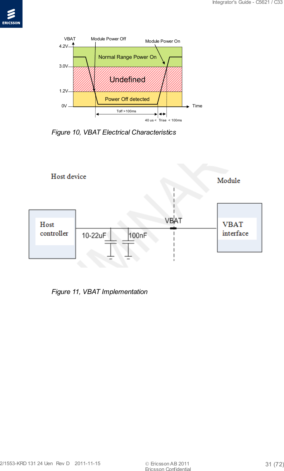
![Integrator's Guide - C5621 / C33 2/1553-KRD 131 24 Uen Rev D 2011-11-15 Ericsson AB 2011 64 (72) Ericsson Confidential 10 Firmware Updates Within a single model of the Mobile Broadband Module, different firmware configuration may be introduced for mainly two reasons: 1. A firmware configuration may be accepted by some mobile operators whereas other may require further changes to be made. This will result in that two or more versions have to be available at the same time. 2. Updated firmware configurations with added features and error corrections are created as maintenance releases, which can be supplied to the end-user for improved performance. The first of these two reasons for different firmware configurations has traditionally resulted in multiple SKUs of the Mobile Broadband Module. The situation is improved now as the module will be able to change firmware configuration automatically, see chapter 10.1. The second reason for different firmware configurations results in that the updated firmware is distributed to the end-user as a firmware updater application to be run on the host device. 10.1 Network Dependent Firmware Updates The Mobile Broadband module has the capability of storing several different firmware configurations in the persistent on-board flash memory. A database containing information about all operators that have approved a specific firmware configuration is stored in the module. When a new firmware configuration is released the database will be updated. During module manufacturing the latest database available is stored in the module memory together with the valid released and approved firmware configurations. During startup, the module will use the UICC card to identify the network operator that is currently used. The module can, based on this information select to use a different firmware configuration. The host software can supply the end user with information regarding the updates as well as provide interfaces for 3rd party applications to implement own support for showing update information. For more information regarding Network dependent firmware updates, see [9].](https://usermanual.wiki/Wistron/TP00043AEF.Integrators-guide/User-Guide-1834315-Page-64.png)
![Integrator's Guide - C5621 / C33 2/1553-KRD 131 24 Uen Rev D 2011-11-15 Ericsson AB 2011 68 (72) Ericsson Confidential 12 References [1] C5621gw Technical Description 1/1550-KRD 131 24 Ericsson AB [2] 3G in Notebooks Guidelines version 4 Copyright © 2007 GSM Association [3] Universal Serial Bus Specification 2.0 Copyright © 2000, Compaq Computer Corporation, Hewlett-Packard Company, Intel Corporation, Lucent Technologies Inc, Microsoft Corporation, NEC Corporation, Koninklijke Philips Electronics N.V. All rights reserved. [4] AT Command Manual 3/1553-KRD 131 15+ Ericsson AB [5] Ericsson Mobile Broadband SDK 1/1550-CXP 901 4397/1 Ericsson AB [6] Connection Profile Updater 1553-CXC 172 8313/1 Ericsson AB [7] MBM Linux Support 1/102 72-HRC 105 042 Ericsson AB [8] MBM Linux Wiki, http://mbm.sourceforge.net [9] Network Dependent Firmware Upgrades 1/1550-KRD 131 18+ Ericsson AB [10] Antenna Performance Guideline 1/1553-FAF 901 658/1 Ericsson AB [11] Evaluating Compliance with FCC Guidelines for Human Exposure to Radiofrequency Electromagnetic Fields OET Bulletin 65 Supplement C (2001-01) [12] Assessment Of Electronic And Electrical Equipment Related To Human Exposure Restrictions For Electromagnetic Fields (0 Hz - 300 GHz) EN 62311:2008 [13] Electronic Industries Association, "EIA Standard RS-232-C Interface Between Data Terminal Equipment and Data Communication](https://usermanual.wiki/Wistron/TP00043AEF.Integrators-guide/User-Guide-1834315-Page-68.png)
![Integrator's Guide - C5621 / C33 2/1553-KRD 131 24 Uen Rev D 2011-11-15 Ericsson AB 2011 69 (72) Ericsson Confidential Equipment Employing Serial Data Interchange", August 1969, reprinted in Telebyte Technology Data Communication Library, Greenlawn NY, 1985, no ISBN [14] Smartcards, UICC-Terminal Interface; Physical and logical Characteristics, ETSI TS 102 221 [15] Wake on Wireless 2/198 10-FAF 901 658/1 Ericsson AB](https://usermanual.wiki/Wistron/TP00043AEF.Integrators-guide/User-Guide-1834315-Page-69.png)
![Integrator's Guide - C5621 / C33 2/1553-KRD 131 24 Uen Rev D 2011-11-15 Ericsson AB 2011 70 (72) Ericsson Confidential 13 Annex 13.1 Test Setup for Measuring Host-Generated Noise For a module integrated in host the total noise density level ( totN) seen at the GPS receiver can be expressed as the sum of different contributions. • Thermal Noise – Generated within the GPS receiver • External Noise – Generated by the laptop • WW AN Noise – Generated by the WWAN transmitter All of these noise sources are uncorrelated and will add up to a total noise density totN at the auxiliary Antenna Reference Port (ARP), according to Equation 1. Equation 1 Total noise level [W/Hz] wwanextttot NNNN ++= The thermal noise density generated by the GPS receiver itself is equal to kTFNt=, where kT is -174 dBm/Hz at room temperature and F is the noise figure, typically 3.5 dB. The noise density generated by the GPS receiver is then calculated to -170.5 dBm/Hz=-116.5 dBm/MHz. The thermal noise is the critical contribution and will set the limit for the GPS performance. Assume that the WWAN radio is disabled, then wwanN can be set to zero and therefore neglected in the further analysis. To minimize the impact of the noise generated outside the GPS receiver a noise margin M is introduced, according to Figure 27. Ntot Nt ∆ Next M Figure 27, Definition of Noise Margin](https://usermanual.wiki/Wistron/TP00043AEF.Integrators-guide/User-Guide-1834315-Page-70.png)
![Integrator's Guide - C5621 / C33 2/1553-KRD 131 24 Uen Rev D 2011-11-15 Ericsson AB 2011 71 (72) Ericsson Confidential The external noise must be lower than the thermal noise to conserve the GPS performance. The main question is how much lower? The noise margin can be expressed as a function of the noise degradation as in Equation 2. Equation 2 Noise Margin [dB] −=∆1101log1010M Equation 2 then plotted in Figure 28 Noise Margin as a function of degradation as function of the degradation. -5,00,05,010,015,020,00,0 1,0 2,0 3,0 4,0 5,0 6,0Degradation [dB]Margin [dB]Noise Margin Figure 28 Noise Margin as a function of degradation It can be seen that if the margin is set to zero, then the degradation is 3 dB. A consequence of this is that the noise generated by the host device must be substantially lower than the internal noise generated by the receiver it self. So if the overall performance shall be conserved we can assume that the total noise level shall be degraded only 1 dB. This assumption gives, according to Figure 28 Noise Margin as a function of degradation , that the margin must be 6 dB and therefore the noise generated by the host device at ARP must be less than -176.5 dBm/Hz=-116.5 dBm/MHz. 13.1.1 Test Setup The test setup for measuring host-generated noise at ARP consists of two host devices:](https://usermanual.wiki/Wistron/TP00043AEF.Integrators-guide/User-Guide-1834315-Page-71.png)