Wistron TP00043AEF 10.1 inch Tablet with 802.11 abgn 1x1 + BT 4.0 User Manual Integrator s Guide C5621 C33
Wistron Corporation 10.1 inch Tablet with 802.11 abgn 1x1 + BT 4.0 Integrator s Guide C5621 C33
Wistron >
Contents
- 1. users guide
- 2. User guide
- 3. user guide
- 4. Integrators guide
- 5. Regulatory notice
Integrators guide

Integrator's Guide - C5621 / C33
OPERATING MANUAL
2/1553-KRD 131 24 Uen Rev D

Integrator's Guide - C5621 / C33
2/1553-KRD 131 24 Uen Rev D 2011-11-15
Ericsson AB 2011
2 (72)
Ericsson Conf idential
© Ericsson AB 2011
All rights reserved. The information in this document is the property of
Ericsson. Except as specifically authorized in writing by Ericsson, the
receiver of this document shall keep the information contained herein
confidential and shall protect the same in whole or in part from disclosure
and dissemination to third parties. Disclosure and disseminations to the
receiver's employees shall only be made on a strict need to know basis.

Integrator's Guide - C5621 / C33
2/1553-KRD 131 24 Uen Rev D 2011-11-15
Ericsson AB 2011
3 (72)
Ericsson Conf idential
Abstract
This document describes the Ericsson Mobile Broadband Module and is
intended to support developers when integrating the product into host devices.
Purpose
The Integrator’s Guide is designed to give the reader a deeper technical
understanding of the Ericsson Mobile Broadband Modules and information
needed for integrating the product into host devices. It also describes the PC
software for the Mobile Broadband Modules that has been developed by
Ericsson.
Trademark and Acknowledgements
Microsoft, Windows, Windows Vista, Internet Explorer, .NET and Outlook are
registered trademarks or trademarks of Microsoft Corporation in the United
States and/or other countries.
Intel is a trademark of Intel Corporation in the United States
Ericsson is a trademark of Telefonaktiebolaget LM Ericsson.
GSM and the GSM Logo are registered and owned by the GSM Association.
PGPS is a trademark of Rx Networks Inc.
Linux® is the registered trademark of Linus Torvalds in the U.S. and other
countries.
All trademarks are the property of their respective owners. All other product or
service names mentioned in this document are trademarks of their respective
companies.

Integrator's Guide - C5621 / C33
2/1553-KRD 131 24 Uen Rev D 2011-11-15
Ericsson AB 2011
4 (72)
Ericsson Conf idential
Contents
1 Introduction .............................................................................................. 6
1.1 Target Users ..............................................................................................6
1.2 Prerequisites ..............................................................................................6
2 Product Details and Key Features ......................................................... 7
2.1 USB Quick Enumeration ............................................................................7
2.2 Always On ..................................................................................................8
2.3 Wake on Wireless ......................................................................................9
2.4 Idle Mode Power Management..................................................................9
2.4.1 USB Selective Suspend...........................................................................10
2.4.2 Continuous Packet Connectivity ..............................................................10
2.4.3 Fast Dormancy .........................................................................................10
2.5 Over-temperature protection....................................................................11
2.5.1 Over-temperature signaling .....................................................................11
2.5.2 GPS Thermal Throttling ...........................................................................11
2.5.3 PA Thermal Throttling ..............................................................................12
3 System Integration Overview ............................................................... 13
3.1 Power On .................................................................................................13
3.2 Power off ..................................................................................................14
3.2.1 Module Restart/Reset ..............................................................................15
3.3 GPS Interface...........................................................................................16
3.3.1 Antenna Recommendations ....................................................................16
3.3.2 External antenna amplifier .......................................................................17
3.3.3 Assisted GPS Features ...........................................................................17
3.3.4 2-antenna version ....................................................................................17
3.4 UICC (USIM Card) ...................................................................................18
3.4.1 UICC Hot Swap........................................................................................19
3.5 Electrostatic Discharge (ESD) Precautions.............................................19
4 Electrical Integration ............................................................................. 20
4.1 Physical size ............................................................................................20
4.2 Pinout .......................................................................................................21
4.3 System Connector ...................................................................................22
4.3.1 Electrical Interface Detail Format ............................................................29
4.3.2 TTL Levels ...............................................................................................29
4.3.3 Power Interfaces ......................................................................................30
4.3.4 Data communication interfaces ...............................................................33
4.3.5 Debug Interface........................................................................................34
4.3.6 Control and Status Interfaces ..................................................................36
4.3.7 UICC Interface .........................................................................................42
4.3.8 PCM 0 & 1 Interface.................................................................................45
4.3.9 RF interface..............................................................................................46
5 Mechanical Dimension .......................................................................... 47
6 Routing guidelines................................................................................. 48

Integrator's Guide - C5621 / C33
2/1553-KRD 131 24 Uen Rev D 2011-11-15
Ericsson AB 2011
5 (72)
Ericsson Confidential
6.1 Recommended PCB Footprint.................................................................48
6.2 Digital I/O routing .....................................................................................49
6.2.1 Clock Routing ...........................................................................................50
6.2.2 USB Routing ............................................................................................50
6.3 Power Routing..........................................................................................51
6.3.1 VBAT Routing ..........................................................................................51
6.3.2 GND .........................................................................................................51
6.4 RF Routing ...............................................................................................51
7 Production Guideline............................................................................. 52
7.1 Package type ...........................................................................................52
7.2 Floor life and dry storage .........................................................................52
7.3 Screen stencil design ...............................................................................52
7.4 Assembly..................................................................................................52
7.5 Reflow soldering.......................................................................................53
8 Packaging – Tape and Reel Information ............................................. 54
9 SW integration........................................................................................ 56
9.1 Driver and Application Architecture .........................................................56
9.1.1 Windows XP and Vista Architecture ........................................................56
9.1.2 Windows 7 Architecture ...........................................................................57
9.1.3 Linux driver architecture ..........................................................................59
9.2 Connection Profile List .............................................................................60
9.3 Ericsson Mobile Broadband C++ API ......................................................60
9.4 State machine ..........................................................................................61
9.5 Service Windows Registry Keys ..............................................................62
9.5.1 Module state.............................................................................................62
9.5.2 TCP/IP Configuration ...............................................................................63
10 Firmware Updates .................................................................................. 64
10.1 Network Dependent Firmware Updates ..................................................64
11 Terminology and abbreviations ........................................................... 65
12 References .............................................................................................. 68
13 Annex ...................................................................................................... 70
13.1 Test Setup for Measuring Host-Generated Noise ...................................70
13.1.1 Test Setup ................................................................................................71

Integrator's Guide - C5621 / C33
2/1553-KRD 131 24 Uen Rev D 2011-11-15
Ericsson AB 2011
6 (72)
Ericsson Confidential
1 Introduction
Ericsson’s C5621/C33 Mobile Broadband Module is a 277 pin LGA
subassembly, which enables end users to have mobile access to the internet
or corporate network with flexibility and high speed, including ‘always online’
capability. It supports data services HSPA Evolution, HSPA, UMTS, EDGE,
GPRS, and SMS. The C5621 module also has an integrated GPS receiver,
which can be used by positioning applications.
The Ericsson Mobile Broadband Module is a solution designed as an add-in
option for various host devices such as netbooks, tablets, Personal Navigation
Devices (PND), e-Readers, handheld gaming devices, cameras and other
consumer devices.
The integration of HSI and SPI are not covered in this document. However,
they will be covered in future revisions.
Product introduction and general information can be found in the Technical
Description and User Guide for the mobile broadband module, see [1].
1.1 Target Users
The Ericsson Mobile Broadband Modules are designed for the embedded
community for integration into any host device. Target focus is mainstream
PC-OEM businesses making slim tablet devices, Personal Navigation Devices
(PND), e-Readers and other consumer devices.
1.2 Prerequisites
Integration of the Ericsson Mobile Broadband Module should be performed at
facilities under host device management. The necessary integration
instruction, driver software and user documentation will be provided. No
special prerequisite knowledge is necessary. In general, it is recommended to
follow the guidelines presented by GSMA for the integration of 3G WWAN
modules into notebook computers, see 3G in Notebooks Guidelines [2].

Integrator's Guide - C5621 / C33
2/1553-KRD 131 24 Uen Rev D 2011-11-15
Ericsson AB 2011
7 (72)
Ericsson Confidential
2 Product Details and Key Features
This section explains the key features of the C5621/C33 Mobile Broadband
modules.
2.1 USB Quick Enumeration
The USB start-up time is defined as the time from the module power-up to
USB enumeration (USB_D+ signal high), and is, normally, less than 3 s. To
further shorten the USB start-up time, quick enumeration can be used as
described below.
The Mobile Broadband Module supports USB quick enumeration to minimize
the time it takes until the USB_D+ signal becomes high. The feature can be
used to improve performance if the host BIOS includes a lock mechanism
which restricts the Mobile Broadband Modules that can be used with the host.
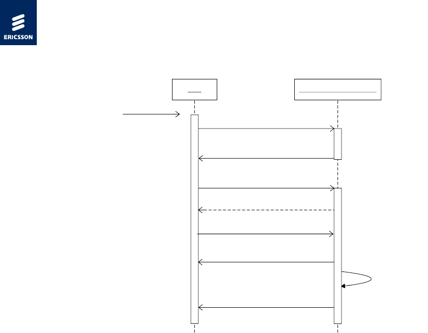
The quick-enumeration process is described below and is depicted in Figure
1.
1 When the module is powered, it will quickly bring up USB functionality to
set the USB_D+ signal high.
2 When the host device detects the module and asks for descriptors, the
module will reply with a descriptor giving VID and PID (PID will not be the
same as in the full enumeration that follows), model name and vendor
name.
3 When the descriptor has been received, the host will send a Set
Configuration command.
4 When the module has replied its descriptor and received the set
configuration command, it will make a soft detach from the USB. If the host
does not ask for the descriptor within a certain time limit, the module will
make a soft detach anyway to continue the module start-up sequence.
5 After the module has made the soft detach, it will make a full enumeration.
The descriptor for the full enumeration will include configuration and
interface descriptors.
Integrator's Guide - C5621 / C33
2/1553-KRD 131 24 Uen Rev D 2011-11-15
Ericsson AB 2011
8 (72)
Ericsson Confidential
Host
Power On
Mobile Broadband Module
Power On
GetDescriptors
Soft Detach
VID, PID model
and vendor name
Continue Start-up
Set Configuration
USB_D+ Quick Enumeration
USB_D+ Full Enumeration
Figure 1, USB quick-enumeration process
2.2 Always On
The Mobile Broadband Module behavior when the host enters Sleep (ACPI
S3) or Hibernate (ACPI S4) is configurable by registry key settings. The
WMCore service can command the module to either shut down or stay
registered to the network - “Alwa ys On”. When the Always On setting is
enabled, the module shall be kept powered-on while the host device goes into
sleep/hibernate. When the Always On setting is disabled, the module power
supply shall be turned off when host device enters Sleep.
If “ Always On” is enabled, the WWAN LED and WWAN disable functionality
shall also be supported by the host device when in S3. This requirement is to
ensure that the WWAN LED indication is available even if the host device is in
Sleep state.
For implementations that do not use the WMCore service, such as Linux or 3rd
party connection managers, the host device software is required to handle the
Always On functionality if implemented.
It is also possible to configure the Mobile Broadband Module to automatically
enable the radio and register to the network without interaction with the host
device software. The module checks this configuration at each start-up and
changes the radio state accordingly. Please refer to ME Radio Policy in the AT
command manual [4].

Integrator's Guide - C5621 / C33
2/1553-KRD 131 24 Uen Rev D 2011-11-15
Ericsson AB 2011
9 (72)
Ericsson Confidential
2.3 Wake on Wireless
The module supports Wake on Wireless (WoW) functionality, i.e. wake the
host from sleep states. The WoW feature requires the host device to have the
Always On feature enabled. The WoW trigger-rules can be set by AT
commands. The WoW functionality can be configured to use the USB
interface or WAKE_N signal to trigger a wake-up signal in order to wake up
the host.
Table 1 WoW support
M ode l Interface Host State (ACPI)
C5621 / C33 USB, WAKE_N
signal
Sleep (S3), Hibernate
(S4) and Off (S5).
The module can be configured to wake the host when an SMS, starting with a
predefined text string (payload) and/or with a predefined originating address,
is received by the module. When an SMS, which corresponds to the above
criteria, is received an unsolicited AT response is generated. The wake event
is signaled using the USB and the normal USB wakeup procedure is triggered.
Additionally it is possible to configure out of band wakeup signaling using the
WAKE_N signal.
In addition to wakeup triggered by SMS, the module can be configured to
wake the host when other predefined events occur, which generate unsolicited
AT responses. Examples are changes in network status, reception of any
SMS and SMS memory full.
If the wake up was triggered by an SMS, the payload can be fetched using the
SDK or AT commands [9] when the host has resumed from its sleep state.
For further details see [15].
2.4 Idle Mode Power Management
The Mobile Broadband Module supports features to minimize power
consumption when in idle mode. Based on the ongoing activities in the
module, the module is able to remove or decrease power in various parts of
the platform.

Integrator's Guide - C5621 / C33
2/1553-KRD 131 24 Uen Rev D 2011-11-15
Ericsson AB 2011
10 (72)
Ericsson Confidential
2.4.1 USB Selective Suspend
The Mobile Broadband Module and the drivers support USB selective
suspend. The USB selective suspend functionality is available for both
Windows and Linux (autosuspend). When there is no communication over the
module’s USB interface, the interface will automatically be suspended
independently of other devices connected to the host device. When the
selective suspend mode is reached the power consumption in the module
decreases significantly, and it also allows the host platform to enter lower
power modes.
To optimize the time the module spends in USB selective suspend, it is
important that software applications on the host device subscribes to events
from the WMCore service or utilize unsolicited AT commands instead of
periodically polling for information. Please see note in chapter 4.3.4.1 for host
design recommendations.
2.4.2 Continuous Packet Connectivity
The C5621 module has support for the CPC feature available in 3GPP release
7. CPC is a set of features to save battery power. The most important features
are DRX and DTX.
DRX (Discontinuous Reception): When module is in HSPA mode it has to
monitor a certain signaling channel from the base station to see if data
packets will be delivered to it in coming time slots. If the data traffic is bursty,
the base station can instruct the module to listen to the signaling channel less
frequently than normal. In this way the module’s receiver can be switched off
and save power.
DTX (Discontinuous Transmission): When module is in HSPA mode it has to
stay synchronized to the base station. The module does this by sending
control information on a dedicated signaling channel to the base station. This
is done continuously. If data traffic is bursty, the base station can let the
module send information in bursts rather than continuously. In this way the
module’s transmitter can be switched off and save power.
The CPC feature also helps to improve the initial data latency which occurs
while moving from the idle channels to high speed data channels. The CPC
feature needs to be supported in the radio network to be effective.
2.4.3 Fast Dormancy
The C5621 module has support for the Fast Dormancy feature. It is a feature
for saving battery life. This functionality enables a way around the network
timers for downgrading from Cell_DCH/Cell_FACH to the least power state in
a faster manner.

Integrator's Guide - C5621 / C33
2/1553-KRD 131 24 Uen Rev D 2011-11-15
Ericsson AB 2011
11 (72)
Ericsson Confidential
The module sends a ‘Signalling Connection Release Indication’ Cause to the
network. The UTRAN (network) upon reception of this IE may decide to trigger
an RRC State transition to a more battery efficient state, ultimately IDLE.
Fast Dormancy is triggered and is steered from the host and it’s a feature
available in 3GPP release 8.
Note: The fast dormancy support in C5621 has one of the timers (T323) set to a
default value of 60 seconds.
2.5 Over-temperature protection
To protect the Mobile Broadband Module hardware from over-heating, and to
ensure radio performance and component life length, the module supports
over-temperature protection.
The over-temperature protection function consists of three parts:
• Over-temperature signaling
• GPS thermal throttling
• PA thermal throttling
2.5.1 Over-temperature signaling
This function reports to the host SW, e.g. connection manager software, when
the temperature passes through some configurable temperature threshold;
refer to the SDK [5] and the AT Command Manual [4] for details.
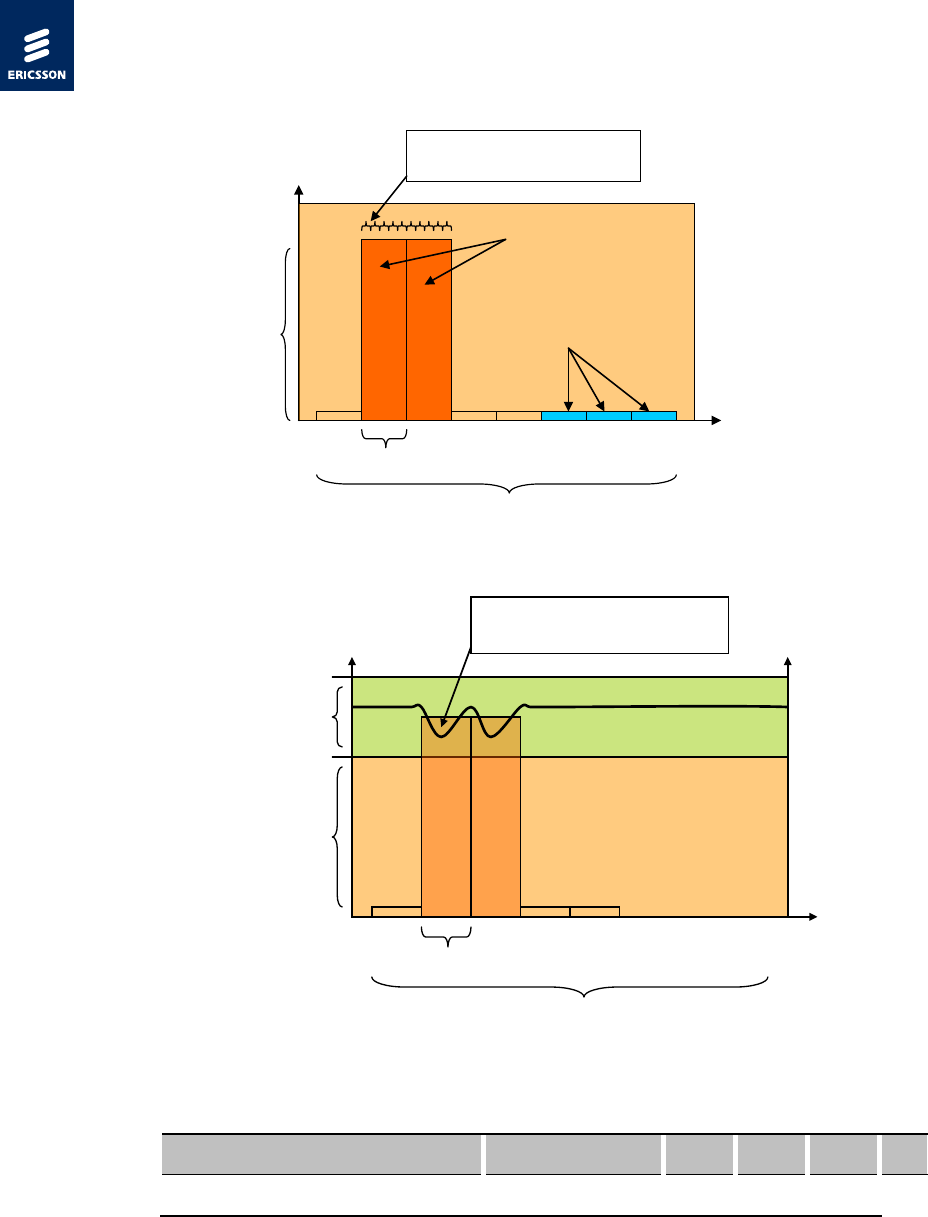
2.5.2 GPS Thermal Throttling
The GPS Thermal Throttling function limits the GPS functionality according to
module temperature. This is done to prioritize module functionality in higher
temperatures.
GPS will automatically turn off when temperature exceeds Threshold A, see
Figure 2. Any changes in the GPS status depending on this function is
reported, unsolicited, to the host software; see the SDK [5] and the AT
Command Manual [4] for details.
Integrator's Guide - C5621 / C33
2/1553-KRD 131 24 Uen Rev D 2011-11-15
Ericsson AB 2011
12 (72)
Ericsson Confidential
Temperature
Threshold A
Time
* Start limited search time,
T_status changes to 1
GPS shut down,
T_status changes to 2
* Search time limited to 90s by default
GPS re-start allowed when
below hysteresis, T_status
changes to 1
GPS operation allowed if
last command was GPS
enable, T_status changes
to 0
Figure 2, GPS Thermal Throttling
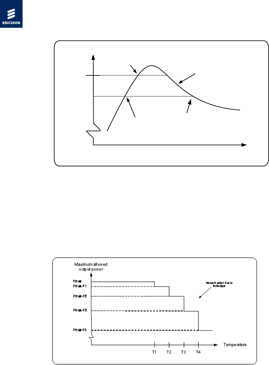
2.5.3 PA Thermal Throttling
The PA Thermal Throttling function limits the output power according to
module temperature. The temperature thresholds and back-off values are set
in module firmware see Figure 3. The decreased maximal output power will
cause the mobile network to take action, for instance limit uplink throughput or
handover to 2G.
Figure 3, Maximal output power reduction due to PA throttling
Integrator's Guide - C5621 / C33
2/1553-KRD 131 24 Uen Rev D 2011-11-15
Ericsson AB 2011
13 (72)
Ericsson Confidential
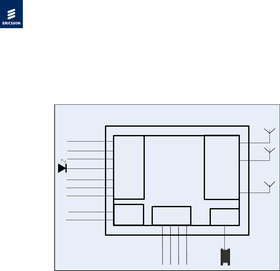
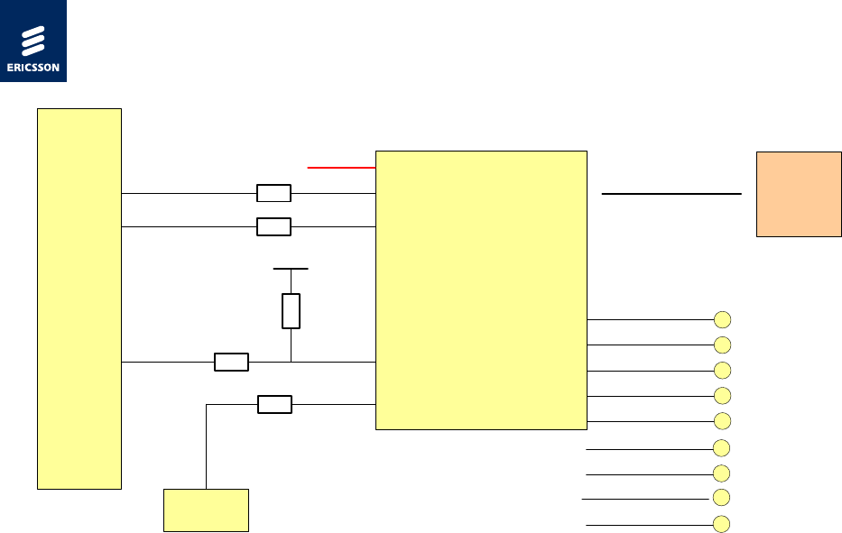
3 System Integration Overview
C5621/ C33 Mobile Broadband Module is a 277 pin LGA SIP module.
Interfaces and functionality needed on the host device side are shown in
Figure 4.
MAIN Antenna
TX/RX
DIV Antenna
WCDMA RX
LED
VBAT
GND
USB
WWAN_Disable_N
WAKE
GPS_Disable_N
GPS Antenna
UART 0 & 1
SPI
POWER_ON
LGA PADS
UICC
Interface
Control &
Status
Interface
Power
Interface
Data
Communication
Interface
HSI
HW_READY
RTC_CLK
RF
Interface
Mobile Broadband Module
C5621 / C3304
Figure 4, Mobile Broadband module interface overview. Please note: HIS and
SPI are for future use. HW_Ready is a signal directed out from the
module. All other signals are directed in to the module.
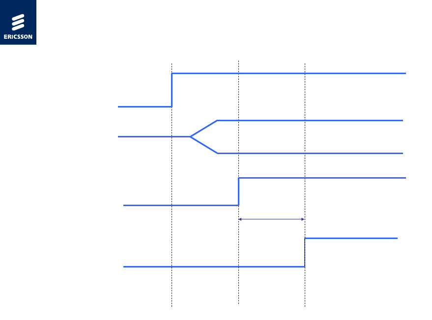
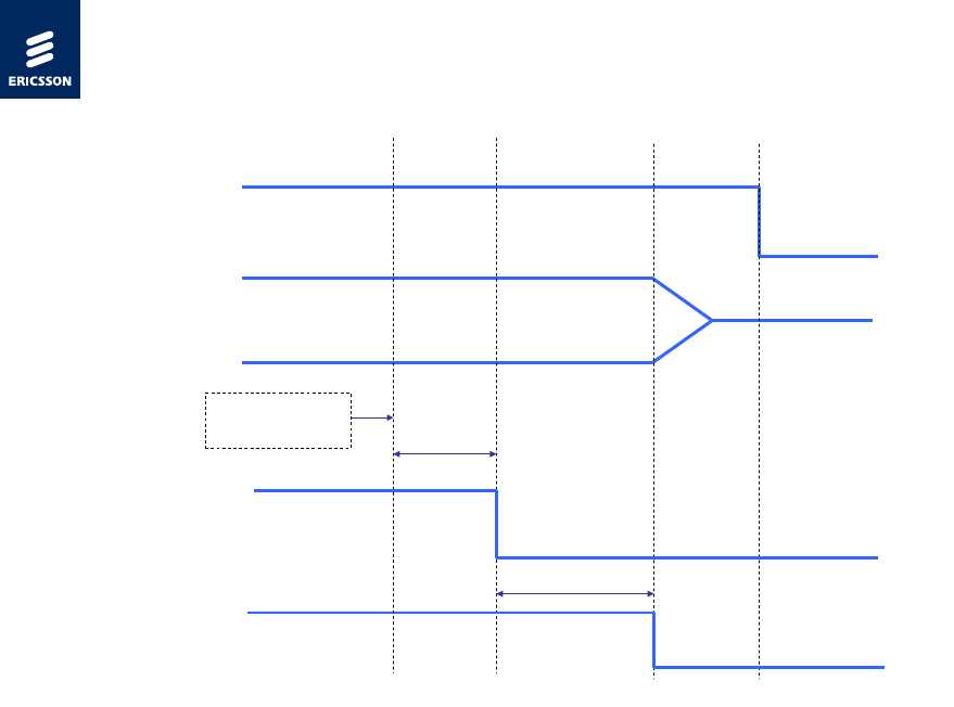
3.1 Power On
The module start-up is controlled by a GPIO signal, POWER_ON. Once VBAT
and RTC_CLK signals are fed to the module, the host device has to drive
POWER_ON signal high for starting the module. The module asserts
HW_READY signal high. Though HW_READY is not an mandatory signal to
setup the interface towards the module, the host system can utilize this signal
to avoid back feeding. Refer to chapter 4.3.5.3 for the signal description. The
power on sequence is explained in Figure 5.
Integrator's Guide - C5621 / C33
2/1553-KRD 131 24 Uen Rev D 2011-11-15
Ericsson AB 2011
14 (72)
Ericsson Confidential
~ 32 ms
HW_READY
POWER_ON
RTC_CLK
VBAT
Figure 5, Example of Module Power on Sequence
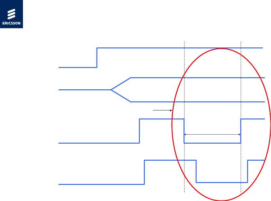
3.2 Power off
The module can be powered off by pulling down the POWER_ON signal low
for minimum 100 μs. The power down sequence is explained in Figure 6.
Though a hardware interface is available for the module shutdown, one shall
use it along with the software method to shutdown the module safely. The
software solution is realized by using a background service (WMCore) in
Windows, which subscribes to Windows OS power events. When the host
switches state into hibernate (ACPI S4) or power off (ACPI S5), a shut down
command is sent to the module. The module will autonomously de-register
from the radio network, save the mobile network list, turn off the radio and shut
down the SIM. Finally the module itself is turned off, including the USB
interface.
The host device designer should keep the power to the module for at least 2
seconds after the Windows OS power event, to ensure that there is time for
the module to shut down properly. The shut down behavior towards the SIM
and network has to comply with 3GPP requirements, please refer to 3GPP TS
24.008 chapter 4.3.4.
Integrator's Guide - C5621 / C33
2/1553-KRD 131 24 Uen Rev D 2011-11-15
Ericsson AB 2011
15 (72)
Ericsson Confidential
~ 100 μs
HW_READY
POWER_ON
RTC_CLK
VBAT
Issue
AT+CFUN=0 ~ 2 s
Figure 6, Example of Module Power down Sequence
Implementations that do not use the background service, such as Linux or 3rd
party connection managers, needs to issue the shutdown command to the
module and wait until the module disables its USB interface before turning off
the power supply to the module. This procedure is recommended to ensure
that the module properly de-registers from the radio network and saves the
current network list. The procedure guarantees quick registration on previous
available radio network during the next power-on cycle.
Please refer to chapter 4.3.3.1 for more information about module electrical
requirements.
3.2.1 Module Restart/Reset
POWER_ON signal can be utilized to reset/restart the C5621/C33 module.
This can be done by driving this signal low for minimum 200 μs before driving
it high again. This will eventually power cycle the module. It is recommended
that this method of module reset shall be utilized only under irrecoverable
error conditions. For other conditions, it is always recommended to do a soft
reset using AT-Command.
Integrator's Guide - C5621 / C33
2/1553-KRD 131 24 Uen Rev D 2011-11-15
Ericsson AB 2011
16 (72)
Ericsson Confidential
≥200 μs
HW_READY
POWER_ON
RTC_CLK
VBAT
Module Reset Cycle
Figure 7, Example of Module Reset Sequence
3.3 GPS Interface
The Mobile Broadband Module supports different kinds of assisted GPS
features, which put requirements on SW to be installed on the host side and in
some use cases also agreements to be signed by the integrator.
3.3.1 Antenna Recommendations
The GPS performance when integrated in a host device is dependent on
antenna efficiency (including cable loss), antenna pattern/polarization and
host-generated noise. The internal noise can be generated from DC/DC
converter, LCD, CPU, hard drives etc and other co-existing radio transceivers
(e.g. WLAN and Bluetooth). To achieve good performance the host-generated
noise level should be less than -116.5 dBm/MHz in 1525.42
±
1 MHz band.
The noise level is not possible to measure with conventional instruments.
However, there is a way to estimate the noise added by the host platform
using an Over-The-Air (OTA) measurement setup. The test setup is described
in chapter 13.1.
General recommendation for designing 3G, 2G and GPS antenna is stated in
the ‘Antenna Performance Guideline’ document [10].

Integrator's Guide - C5621 / C33
2/1553-KRD 131 24 Uen Rev D 2011-11-15
Ericsson AB 2011
17 (72)
Ericsson Confidential
3.3.2 External antenna amplifier
If an external antenna amplifier is to be used, the gain of the amplifier coupled
with front end losses in cables and other components must be considered. If
strong jammers are picked up by the antenna and after that amplified by the
antenna amplifier there is a risk that the LNA in the C5621 gw module will
work in the nonlinear area and thereby degrading performance of the GPS.
Therefore, if an antenna amplifier is to be used, try to avoid placing
transmitting antennas close to the GPS antenna and do not use a more
powerful antenna amplifier than necessary. I.e. the amplifier does not add any
performance improvement by amplifying the signals more than losses in
cables and passives before entering the LNA in the C5621 gw module.
3.3.3 Assisted GPS Features
Assisted GPS can be divided into Internet-assisted and network-assisted
GPS. There exist multiple variants of both Internet- and network-assisted
GPS.
Table 2 Assisted GPS features in Mobile Broadband Modules
M ode l A-GPS
Technologies
Internet Assisted
Variant
Network Assisted
Variant
C5621
Extended
Ephemeris,
SUPL
PGPS (RX Networks) OMA SUPL 1.0
Internet-assisted GPS is based on the ephemeris data that is downloaded
over Internet and transferred to the module. To collect the ephemeris data,
proprietary code of the provider of the Internet-assisted service (stated in
Table 2) need to be run. The proprietary code is included in Ericsson’s PC
software for Windows.
3.3.4 2-antenna version
In the case that 2 antennas are preferred and main and diversity functionality,
as well as GPS functionality is required, a split of antenna signals is needed
outside the C5621 gw module.
An example of how this can be achieved is illustrated in Figure 8 below.

Integrator's Guide - C5621 / C33
2/1553-KRD 131 24 Uen Rev D 2011-11-15
Ericsson AB 2011
18 (72)
Ericsson Confidential
GPS
1μ
22 p
nm
47n
nm
12
3 4
56
Ubat
On C56 module
To WCDMA div
GPS extractor
component
Figure 8 Example of antenna signal split for 2 antenna version
The “GPS extractor component” in Figure 8 can be chosen as follows:
TDK-EPC: B39162B7742E310
Taiyo Yuden: G6KU1G575L4WF
Be careful to read the application note of the chosen “GPS extractor
component” in order to include matching components or other external
components in the design.
Also included in the illustration in Figure 8 is an example of how an antenna
amplifier can be power fed. Be aware that capacitors and inductors must not
be omitted. This is in order not to risk damaging components or degrade
performance of the system.
The signal trace from the antenna to the C5621 gw module is carrying RF
signals. Thus, the trace must refer to a ground plane and the trace width must
be calculated by considering the distance to the ground plane and the
dielectric constant of the circuit board used. For all RF signals it is really
important not to place them close to any source of distortion such as digital
signals, clock signals, power signals or any other signal with sharp transients
or high power.
Preferably the antenna should be placed as close as possible to the module to
minimize signal losses and risks for distortions being picked up.
3.4 UICC (USIM Card)
An external SIM card with 3 V or 1.8 V technology must be connected to the
Mobile Broad Band Module via the UIM interface pins. It is recommended that
the host device design minimizes the connection length between the Ericsson
Mobile Broadband Module and the UICC reader. It is also recommended to
minimize the potential for coupling of interfering signals to the UICC interface.

Integrator's Guide - C5621 / C33
2/1553-KRD 131 24 Uen Rev D 2011-11-15
Ericsson AB 2011
19 (72)
Ericsson Confidential
Note: The UICC design (UICC reader, signal strength and integrity), is part of the
3GPP testing on system level.
Note: UICC electrical requirements are not guaranteed by the module in the event of
UICC Hot swap. Host device design is required to choose a UICC socket
which offers such protection.
Note: This is a software-based solution. The SIM_OFF signal is not used.
3.4.1 UICC Hot Swap
The Mobile Broadband module will autonomously detect and reset its internal
logic to handle a UICC hot swap. The module can be configured to send an
unsolicited AT response when a UICC removal event is registered. When a
UICC detection event is registered, the host will be alerted by an unsolicited
response before the module is automatically restarted. The WMCore service
handles this logic and will issue UICC event notifications on the C++ API [5].
The host must be prepared for an automatic module restart when a UICC
detection event is registered. For implementations that do not use the
WMCore service, such as Linux or 3rd party connection managers, the host
device software is required to handle the UICC hot swap functionality, if
implemented.
3.5 Electrostatic Discharge (ESD) Precautions
The Ericsson Mobile Broadband Module is Electrostatic Discharge (ESD)
protected. However, it is recommended that integrators follow electronic
device handling precautions when working with any electronic device system
to prevent damage to the host or the radio device.
When the Ericsson Mobile Broadband Module is mounted in the host, it is the
responsibility of the integrator to ensure that static discharge protection is
designed in to the host product. If exposed, the antenna and UICC interfaces
are vulnerable contact points for ESD.

Integrator's Guide - C5621 / C33
2/1553-KRD 131 24 Uen Rev D 2011-11-15
Ericsson AB 2011
20 (72)
Ericsson Confidential
4 Electrical Integration
This chapter describes the electrical interface between the Ericsson Mobile
Broadband Module and the host device. A summary of the function of each
signal is provided, together with any additional relevant information.
Signals are described from the perspective of the Ericsson Mobile Broadband
Module. Consequently, signals described as ‘Input’ are input signals to the
module, driven by the host [Host ⇒ Module]. Likewise, signals described as
‘Output’ are driven by the module into the host [Module ⇒ Host]. Bi-directional
signal flow (I/O) is indicated by a double-headed arrow [Module ⇔ Host]. In
cases like UICC interface, which utilizes the host circuitry to interface to the
module, it will be indicated as an interface between the module and the
respective component, like [Module ⇒ UICC].
Apart from the module soldering process, the system radio performance
depends also on host system design, host device noise, antenna design and
performance etc. The host antenna system design is very important for total
radio performance. For minimal system 3G performance recommendations
see [2]. Note that the operators may have stricter radio performance
requirements than stated in [1].
This equipment complies with FCC radiation exposure limits set forth for an
uncontrolled environment if the equipment is installed and operated with
minimum distance of 20 cm between the radiator and your body. Depending
on host design and antenna location there are requirements on human body
exposure to RF emissions, please refer to [11] and [12] for more information.
The transmitter must not be co-located or operating in conjunction with any
other antenna or transmitter.
4.1 Physical size
Width: 29 (±0.1) mm
Length: 29 (±0.1) mm
Height: < 1.99 (±0.1) mm
Integrator's Guide - C5621 / C33
2/1553-KRD 131 24 Uen Rev D 2011-11-15
Ericsson AB 2011
21 (72)
Ericsson Confidential
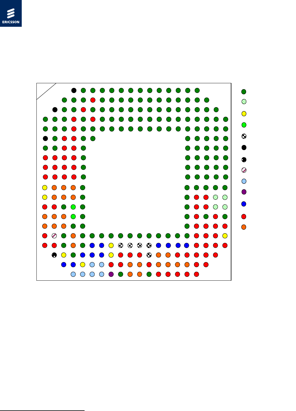
4.2 Pinout
The pin out is configured as a 277 pin LGA. Pad diameter is 0.63mm, pitch
1.27mm. The coordinate F6 in Figure 8 is the reference point.
GND
VBAT
Control & Status
USB
UICC
RF
TP
SYS_CLK
UART
RTC_CLK
Reserved
NC
Future Use
1 2 3 4 5 6 7 8 9 10 11 12 13 14 15 16 17 18 19 20
A
B
C
D
E
F
G
H
J
K
L
M
N
P
R
T
U
V
W
Y
GND
VBAT
Control & Status
USB
UICC
RF
TP
SYS_CLK
UART
RTC_CLK
Reserved
NC
Future Use
Figure 9, C5621/C33 Top View (looking through the module) 1. The coordinate
F6 is the reference point.
1 Please use electronic format to vi ew this fi gure to get better clarity on the details

Integrator's Guide - C5621 / C33
2/1553-KRD 131 24 Uen Rev D 2011-11-15
Ericsson AB 2011
22 (72)
Ericsson Confidential
4.3 System Connector
All signals are routed through the LGA pads for interfacing with the host
device - power, ground, data, control, status and UICC interface.
Table 3, Pin List
Pin Name Function
A4 RF_ MAIN Main RF Interface for GSM and WCDMA
A5 GND
A6 GND
A7 GND
A8 GND
A9 GND
A10 GND
A11 GND
A12 GND
A13 GND
A14 GND
A15 GND
A16 GND
A17 GND
B3 GND
B4 GND
B5 GND
B6 Reserved NC1
B7 GND
B8 GND
B9 GND
B10 GND
B11 GND
B12 GND
B13 GND
B14 GND
B15 GND
B16 GND
B17 GND
B18 GND
C2 RF_GPS GPS Receiver RF Interface
C3 GND
C4 GND
C5 Reserved NC
1
C6 GND
C7 GND

Integrator's Guide - C5621 / C33
2/1553-KRD 131 24 Uen Rev D 2011-11-15
Ericsson AB 2011
23 (72)
Ericsson Confidential
Pin Name Function
C8 GND
C9 GND
C10 GND
C11 GND
C12 GND
C13 GND
C14 GND
C15 GND
C16 GND
C17 GND
C18 GND
C19 GND
D1 GND
D2 GND
D3 GND
D4 Reserved NC
1
D5 GND
D6 Reserved NC
1
D7 GND
D8 GND
D9 GND
D10 GND
D11 GND
D12 GND
D13 GND
D14 GND
D15 GND
D16 GND
D17 GND
D18 GND
D19 GND
D20 GND
E1 GND
E2 GND
E3 GND
E4 Reserved NC
1
E5 GND
E6 GND
E7 GND
E8 GND
E9 GND
E10 GND

Integrator's Guide - C5621 / C33
2/1553-KRD 131 24 Uen Rev D 2011-11-15
Ericsson AB 2011
24 (72)
Ericsson Confidential
Pin Name Function
E11 GND
E12 GND
E13 GND
E14 GND
E15 GND
E16 GND
E17 GND
E18 GND
E19 GND
E20 GND
F1 RF_DIV RF Interface for WCDMA Diversity
F2 GND
F3 Reserved
NC1
F4 Reserved
NC1
F5 GND
F6 GND
F16 GND
F17 GND
F18 GND
F19 GND
F20 GND
G1 GND
G2 GND
G3 Reserved
NC1
G4 Reserved
NC1
G5 GND
G16 GND
G17 GND
G18 GND
G19 GND
G20 GND
H1 Reserved
NC1
H2 Reserved
NC1
H3 Reserved
NC1
H4 Reserved
NC1
H5 GND
H16 GND
H17 GND
H18 GND
H19 GND
H20 GND
J1 Reserved NC
1

Integrator's Guide - C5621 / C33
2/1553-KRD 131 24 Uen Rev D 2011-11-15
Ericsson AB 2011
25 (72)
Ericsson Confidential
Pin Name Function
J2 Reserved
NC1
J3 Reserved
NC1
J4 Reserved
NC1
J5 GND
J16 GND
J17 GND
J18 GND
J19 GND
J20 GND
K1 Reserved
NC1
K2 Reserved
NC1
K3 Reserved
NC1
K4 Reserved
NC1
K5 GND
K16 GND
K17 GND
K18 GND
K19 GND
K20 GND
L1 GPS_DISABLE_N GPS RX Disable
L2 HSI_ACDATA HSI 1
L3 HSI_ACFLAG HSI
1
L4 HSI_CAREADY HSI
1
L5 GND
L16 GND
L17 GND
L18 GND
L19 GND
L20 GND
M1 WAKE_N Host Wake up signal
M2 HSI_CADATA HSI
1
M3 HSI_CAFLAG HSI
1
M4 HSI_ AC R EAD Y HSI
1
M5 GND
M16 GND
M17 Reserved
NC1
M18 Reserved
NC1
M19 VB AT Power supply
M20 VB AT Power supply
1 Referenced for future use; Leave open in the host design
2 Referenced for future use; Pull low or tie to GND in the host design

Integrator's Guide - C5621 / C33
2/1553-KRD 131 24 Uen Rev D 2011-11-15
Ericsson AB 2011
26 (72)
Ericsson Confidential
Pin Name Function
N1 Reserved
NC1
N2 Reserved
NC1
N3 GND
N4 USB_DP USB 2.0
N5 GND
N16 GND
N17 Reserved NC
1
N18 Reserved NC
1
N19 VB AT Power supply
N20 VB AT Power supply
P1 IPC _ C A_ WAKE HSI/SPI
1
P2 SPI0_MOSI SPI
1
P3 SPI0_CLK SPI
1
P4 USB_DM USB 2.0
P5 GND
P16 GND
P17 Reserved NC
1
P18 GND
P19 Reserved NC
1
P20 GND
R1 IPC_AC_WAKE HSI/SPI 1
R2 SPI0_CS0 SPI
1
R3 SPI0_MISO SPI
1
R4 GND
R5 GND
R16 GND
R17 Reserved
NC1
R18 Reserved
NC1
R19 Reserved
NC1
R20 Reserved
NC1
T1 Reserved
NC1
T2 SYSCLK Reference WWAN System Clock
T3 GND
T4 HSIC_STROBE HSIC
1
T5 GND
T6 GND
T7 GND
T8 GND
T9 GND
T10 GND
1 Referenced for future use; Leave open in the host design
2 Referenced for future use; Pull low or tie to GND in the host design

Integrator's Guide - C5621 / C33
2/1553-KRD 131 24 Uen Rev D 2011-11-15
Ericsson AB 2011
27 (72)
Ericsson Confidential
Pin Name Function
T11 GND
T12 GND
T13 GND
T14 GND
T15 GND
T16 GND
T17 Reserved
NC1
T18 Reserved
NC1
T19 Reserved NC
1
T20 POWER_ON Module Power On / Reset control
U1 Reserved NC
1
U2 AU X_5V NC
1
U3 GND
U4 HSIC_DATA HSIC
1
U5 GND
U6 Reserved
NC1
U7 Reserved
NC1
U8 WWAN_LED
LED interface for WWAN status indication
U9 U IM_S I MO FF_ N UICC
U10 UIM_CLK UICC
U11 UIM_DATA UICC
U12 UIM_ PWR UICC
U13 Reserved
NC1
U14 Reserved
NC1
U15 Reserved
NC1
U16 Reserved
NC1
U17 Reserved NC
1
U18 Reserved NC
1
U19 RESET_N NC
1
U20 Reserved NC
1
V2 TEST_PIN Test Pin to be terminated on a TP
V3 WWAN_DISABLE_N Radio Disable Control
V4 GND
V5 Reserved NC
1
V6 Reserved NC
1
V7 Reserved NC
1
V8 TX_ ON GSM TX Burst Indication
V9 Reserved NC
1
V10 SW_READY HIS/SPI
1
V11 Reserved NC
1
1 Referenced for future use; Leave open in the host design
2 Referenced for future use; Pull low or tie to GND in the host design

Integrator's Guide - C5621 / C33
2/1553-KRD 131 24 Uen Rev D 2011-11-15
Ericsson AB 2011
28 (72)
Ericsson Confidential
Pin Name Function
V12 UIM_RST UICC
V13 PCM1_ULD PC M1
2
V14 PCM1_SCK PC M1
2
V15 Reserved
NC1
V16 Reserved
NC1
V17 Reserved
NC1
V18 Reserved
NC1
V19 Res erved
NC1
W3 Reserved
NC1
W4 Reserved
NC1
W5 HW_READY Module start-up indication
W6 UART0_CTS UART0
W7 UART0_RTS UART0
W8 Reserved
NC1
W9 Reserved
NC1
W10 PCM0_DLD PCM0
2
W11 PCM0_WS PCM0
2
W12 Reserved NC
1
W13 PCM1_WS PCM1
2
W14 PCM1_DLD PCM1
2
W15 SMB_CLK SMB 1
W16 SMB_DATA SMB
1
W17 Reserved
NC1
W18 Reserved
NC1
Y4 UART1_TX UART1
Y5 UART1_RX UART1
Y6 UART0_TX UART0
Y7 UART0_RX UART0
Y8 RTC_CLK 32kHz Module Boot-up Clock
Y9 GND
Y10 PCM0_ULD PC M0
2
Y11 PCM0_SCK PC M0
2
Y12 GND
Y13 Reserved
NC1
Y14 Reserved
NC1
Y15 Reserved
NC1
Y16 Reserved
NC1
Y17 Reserved
NC1
1 Referenced for future use; Leave open in the host design
2 Referenced for future use; Pull low or tie to GND in the host design

Integrator's Guide - C5621 / C33
2/1553-KRD 131 24 Uen Rev D 2011-11-15
Ericsson AB 2011
29 (72)
Ericsson Confidential
4.3.1 Electrical Interface Detail Format
The description of each interface follows a common format. An example is
shown below:
Interface name: Name of the interface. Preferably, this is the actual name
of the interface in the pin list, but some interfaces are
grouped and the interface name is a collection of interface
signals.
Function: Describe the basic function of the interface; some
interface signals are grouped according to function.
Description: Basic description of the interface and the relationship to
the host.
Signal name: All signal names associated to the interface, all names are
given
Direction: Signal flow direction.
If not used: Specific details for each signal how to terminate the
physical connection if not used by the host. Failure to
observe this convention can result in unpredictable
behavior.
LVTTL: TTL signal level.
Details: Any specific details noted.
4.3.2 TTL Levels
The table below defines the TTL levels of C5621/ C33 Mobile Broadband
Module.
Table 4 TTL signal level definitions
Voltage level 1.8V
VMax VHigh + 0.3
VHigh 1.8
VOutHigh >1.35
VInHigh
>1.17
VThreshold 0.9
VInLow
<0.63
VOutLow
<0.45
VLow 0
VMin -0.3

Integrator's Guide - C5621 / C33
2/1553-KRD 131 24 Uen Rev D 2011-11-15
Ericsson AB 2011
30 (72)
Ericsson Confidential
4.3.3 Power Interfaces
This chapter describes the power, ground and other signals that control or
indicate power states.
• VBAT
• GND
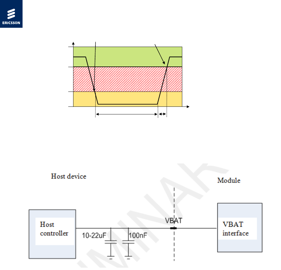
4.3.3.1 VB AT
Function: Power supply
Description: Voltage supply to module
Signal name: VBAT
Direction: Host => Module
If not used: Required
LVTTL: N/A
Details: Voltage provided by the host must range within 3.0V
(minimum) to 4.2V (maximum), the typical value being
3.6V. It is essential that the host platform provides
sufficient voltage during peak current conditions.
Note: The supported voltage range is absolute and including voltage ripple and
glitches. Function and performance are undefined outside supported range.
Note: When turning off the power to the module, the host has to ensure the VBAT
voltage is less than 1.2 V during 100 ms time frame, in order for the module
to properly enter its power-off state. Please refer to parameter Toff in Figure 9.
Note: When turning on the power to the module, the host has to ensure that the
VBAT power on ramp time is kept above 40µs and below 100 ms. The slope
must be monotonous and the ramp times are specified from 10% to 90% of
VBAT. Please refer to parameter Trise in Figure 10.
Note: There is a limited amount of power supply capacitance mounted on the
module. It is essential that the host platform provides sufficient voltage during
the peak current conditions. There should also be decoupling (10-22uF)
located close to the VBAT pins on the module. Make sure that VBAT has a
low impedance connection directly to a battery source. Please refer to Figure
11.
Note: When designing the power supply on the host side, the bursty nature of GS M
TDMA transmission should be taken into consideration. Please refer to
Figure 12 and Figure 13
Integrator's Guide - C5621 / C33
2/1553-KRD 131 24 Uen Rev D 2011-11-15
Ericsson AB 2011
31 (72)
Ericsson Confidential
Time
VBAT
Undefined
3.0V
Normal Range Power On
4.2V
0V
1.2V
Power Off detected
Module Power Off Module Power On
Toff >100ms
40 us < Tri s e < 100ms
Figure 10, VBAT Electrical Characteristics
Figure 11, VBAT Implementation
Integrator's Guide - C5621 / C33
2/1553-KRD 131 24 Uen Rev D 2011-11-15
Ericsson AB 2011
32 (72)
Ericsson Confidential
Time
Power
Consumption
TDMA Frame (4.615 ms)
Timeslot (~577 µs)
Peak 2.50A averaged over a
100µs window in TX burst
Transmit bursts
Peak
Power
Consumption
Receive bursts
Figure 12, Example GPRS/EDGE 3+2 multislot transmission
Time
VB AT
3.0V
4.2V
Operating range
Non operating range
TDMA Fram e (4.615 ms)
Timeslot (~577 µs)
VBAT must never drop below
3.0V during TX burst
Transmit bursts
Figure 13, VBAT during GPRS/EDGE TX burst
Table 5, VBAT Electrical Characteristics
Parameter Condition Low Mid High Unit
Voltage 3.0 3.6 4.2V V
4.3.3.2 GND
Function: Ground
Description: Ground connection(s)
Signal name: GND

Integrator's Guide - C5621 / C33
2/1553-KRD 131 24 Uen Rev D 2011-11-15
Ericsson AB 2011
33 (72)
Ericsson Confidential
Direction: N/A
If not used: Required
LVTTL: N/A
Details: Return path for all currents and ground reference.
4.3.4 Data communication interfaces
4.3.4.1 USB 2.0
Function: USB2.0 data communication port
Description: USB transmit and receive port for data communication
between module and host
Signal name: USB_DP
USB_DM
Direction: Module host
If not used: Required
LVTTL: N/A
Details: The module USB interface is designed to the High Speed
USB specifications; see Universal Serial Bus Specification
2.0 [3].
Power to the USB interface is provided by VBAT input
from the host. The USB start-up time, i.e. from module
startup to D+ high, is less than 3 s. The module has
support for quick enumeration which allows for even
shorter BIOS detection times, please see chapter 2.1
Note: Ericsson strongly recommends that the USB is connected directly to the root
HUB, which is not shared with other USB devices. This ensures that the
module USB selective suspend function is not limited by other devices
connected to the same HUB.
Note: To achieve full throughput performance, the USB host controller should
adhere to USB2.0 specification and be configured for High Speed Mode.

Integrator's Guide - C5621 / C33
2/1553-KRD 131 24 Uen Rev D 2011-11-15
Ericsson AB 2011
34 (72)
Ericsson Confidential
4.3.5 Debug Interface
UART 0 & 1 signals are used for debugging purpose, when USB interface is
disconnected or suspended. Signals shall be routed to test pads or to a test
connector. All signals shall be placed on the same side of the board, for the
ease of accessibility. UART0 CTS & RTS signals can be left as ‘NC’ as they
are not utilized for debugging purpose. Added to this, TEST_PIN (Pin V2) shall
be placed along with these UART signals for debugging. There is
cable detection functionality. Thus, if the signal goes low on these lines then
the module will not go to suspend.
It is rec ommended that the mentioned signals are routed to test pads or test
connector since Ericsson will use them for claims purposes.
Along with the UART signals, USB_DN, USB_DP and RTC_CLK signals from
the module shall be terminated on test pads. These signals shall be used for
debugging the module in the stand-alone mode. The recommendations for
stand-alone mode are described further in this section.
4.3.5.1 UART0
Function: UART0 data communication port (for debugging)
Description: UART data communication port with flow control
Signal name: UART0_TX
UART0_RX
UART0_ RTS
UART0_ CTS
Direction: Module host
If not used: Leave open
LVTTL: 1.8V
Details: 115200 baud, 8 data bit, 1 stop bit, no parity, flow control.
Electrical specification and signaling levels according to
[13].
This port is used for debugging purpose.
4.3.5.2 UART1
Function: UART1 data communication port (for debugging)
Description: UART data communication port without flow control
Signal name: UART1_TX
UART1_RX
Direction: Module host

Integrator's Guide - C5621 / C33
2/1553-KRD 131 24 Uen Rev D 2011-11-15
Ericsson AB 2011
35 (72)
Ericsson Confidential
If not used: Leave open
LVTTL: 1.8V
Details: 115200 baud, 8 data bit, 1 stop bit, no parity, no flow
control.
Electrical specification and signaling levels according to
[13].
This port is used for debugging purpose.
4.3.5.3 Interface for Stand-alone Debug Mode
Ericsson recommends the device integrators to provide an option to start up
the module in ‘stand alone’ debug mode. This interface will primarily be used
for debugging during the R&D phase of the device integrators and by Ericsson
personnel during claims process.
The intention of defining this interface is to test the C5621/C33 module stand-
alone, if any issues in the system functionality or performance is reported. This
will help to isolate the root cause of the issue.
To start up the module in stand-alone, the following recommendations are to
be considered:
• There shall be possibility to power-up the module in the stand-alone
mode, preferably from an external power source (VBAT), bypassing
the host power-on control logic. The corresponding reference GND
shall also be provided on a test pad.
• RTC_CLK (32.768kHz) shall be available to start up the module in this
mode. Terminating RTC_CLK to a test pad enables the possibility to
connect this signal to an external clock source.
• A default pull-up option for POWER_ON signal enables the module to
power-up even when this signal is isolated from the host control logic.
• Possibility to connect USB traces to an external host – by soldering
cable to the test pads or by routing USB traces to a test USB
connector.
• Series zero ohm resistors are to be provided on USB_DP, USB_DN,
POWER_ON and RTC_CLK signals so that these signals can be
isolated to the external test pads in the stand-alone mode.
• UICC interface on the host PCB shall be available, by default, so that
the module is able to communicate with the SIM.
The mentioned signals along with the UART signals and TEST_PIN shall be
placed in the same order as indicated in Figure 14, - pin 1 being referred as
UART0_RX.
Integrator's Guide - C5621 / C33
2/1553-KRD 131 24 Uen Rev D 2011-11-15
Ericsson AB 2011
36 (72)
Ericsson Confidential
VBAT
N4
P4
USB_DN
USB_DP
0 ohm
0 ohm
1.8(VBAT)
100kohm
RTC_CLK
POWER_ON
0 ohm
UICC Interface
SIM
Connector
C5621/C33
T20
Y8
UART0_TX
UART0_RX
UART1_TX
UART1_RX
TEST_PIN
Y4
Y5
Y6
Y7
V2
Host
32.768kHz
0 ohm
RTC_CLK
USB_DN
USB_DP
REF_GND
Figure 14 Stand alone setup for C5621/C33
4.3.6 Control and Status Interfaces
The Control and Status interfaces consist of the following signals:
• WAKE_N
• WWAN & GPS Disable
• WW AN LED
• HW Ready
• TX_ON
• POWER_ON
• RTC CLK
• SYSCLK
4.3.6.1 WWAN_DISABLE_N
Function: Wireless disable input signal
Description: Active low input to disable radio functionality
Signal name: WWAN_DISABLE_N
Direction: Host => module
If not used: Leave open
LVTTL: 1.8V
Details: The function of the WWAN_DISABLE_N signal is
dependant on the software configuration of the

Integrator's Guide - C5621 / C33
2/1553-KRD 131 24 Uen Rev D 2011-11-15
Ericsson AB 2011
37 (72)
Ericsson Confidential
GPS_DISABLE_N signal.
The GPS_DISABLE_N signal can be configured as
disabled (default) or enabled.
When the GPS_DISABLE_N signal is disabled through
software configuration, all radio transmitters and receivers
will be disabled when the WWAN_DISABLE_N signal is
asserted.
When the GPS_DISABLE_N signal is enabled through soft ware
configuration, all radi o transmitters and rec eivers except the
GPS recei ver will be disabled when the WWAN_DISABLE_N
signal is asserted. The signal is internally pulled high to 1.8V
supply with 100kOhm.
Note: The host has to ensure that the WWAN_DISABLE_N signal is not
driven high when VBAT is powered down.

Integrator's Guide - C5621 / C33
2/1553-KRD 131 24 Uen Rev D 2011-11-15
Ericsson AB 2011
38 (72)
Ericsson Confidential
4.3.6.2 GPS_DISABLE_N
Function: GPS disable input signal
Description: Active low input to disable GPS functionality
Signal name: Note: The host has to ensure that the
WWAN_DISABLE_N signal is not driven high when VBAT
is powered down.
GPS_DISABLE_N
Direction: Host => module
If not used: Leave open
LVTTL: 1.8V
Details: Signal is used in conjunction with WWAN_DISABLE_N.
The function of GPS_DISABLE_N is software
configurable in two states; enabled and disabled.
When GPS_DISABLE_N signal is enabled through
software configuration, the GPS receiver shall be disabled
when the signal is asserted.
When GPS_DISABLE_N signal is disabled through
software configuration, nothing shall happen when the
signal is asserted.
Note: The host has to ensure that the GPS_DISABLE_N signal is not driven high
when VBAT is powered down.
Note: The module must be customized to allow the signal to control the GPS. The
default configuration uses the WWAN_DISABLE_N signal to disable both
WWAN and GPS functions.
4.3.6.3 W AK E _ N
Function: Wake up host signal
Description: Wake up the host, active low
Signal name: WAKE_N
Direction: Module => host
If not used: Leave open
LVTTL: 1.8V
Details: The WAKE_N pin can be used to provide an out-of-band
signal for waking up the host device from sleep states.

Integrator's Guide - C5621 / C33
2/1553-KRD 131 24 Uen Rev D 2011-11-15
Ericsson AB 2011
39 (72)
Ericsson Confidential
4.3.6.4 WWAN_LED
Function: Wireless WAN LED control
Description: LED control
Signal name: WWAN_LED
Direction: Module => host
If not used: Leave open
LVTTL: N/A
Details: The Ericsson Mobile Broadband Module uses this pin for
LED control. The pin is driven as a current sink of
approximately 10mA maximum.
The LED will reflect the current WWAN radio status. If the
WWAN radio is on, the led will be lit and vice versa.
Note: It is recommended that the power supply for the LED is disabled when the
VBAT power rails are disabled.
Table 6, WWAN_LED Electrical Characteristics
Parameter Condition Min T yp Max Unit
WWAN_LED
ON - 10 - mA
OFF High Z
Input voltage
level 5.5 V
4.3.6.5 HW_READY
Function: Status signal intended for preventing back
feeding
Description: Status signal for host I/O.
Signal name: HW_REA DY
Direction: Module => host
If not used: Leave open
LVTTL: 1.8V
Details: The signal has an initial low state from the start-
up of the module. The signal is indicating the

Integrator's Guide - C5621 / C33
2/1553-KRD 131 24 Uen Rev D 2011-11-15
Ericsson AB 2011
40 (72)
Ericsson Confidential
modules on/off/reset state.
• Via a low signal is the module indicating a
power off or a reset state.
• Via a high signal is the module indicating
a power on state.
When the HW_READY signal is high, the host
can set the interfaces without risk for current
leakage.
4.3.6.6 POWER_ON
Function: Signal to turn on the module
Description: Active high signal to start the module
Signal name: POWER_ON
Direction: Host => module
If not used: Required
LVTTL: 1.8V (VBAT Compatible)
Details: The POWER_ON signal is used by the host to start up the
module. This signal is level-sensitive.
A high level on POWER_ON triggers the module start up
sequence. The POWER_ON signal is internally gated with
the 32kHz clock input signal (RTC_CLK). After 1024
pulses (32ms) the modem starts the boot process.
The module has an internal pull down and requires the
host system to drive this signal HIGH to start the module.
The host controller must pull this pin high in order for the
module to startup.
4.3.6.7 TX_ON (For Future Use)
Function: Indicate GSM TX burst
Description: Active high signal sent during entire GSM TX burst
Signal name: TX_ON
Direction: Module => host
If not used: Leave open
LVTTL: 1.8V
Details: Intended to be used for GSM TX burst masking.

Integrator's Guide - C5621 / C33
2/1553-KRD 131 24 Uen Rev D 2011-11-15
Ericsson AB 2011
41 (72)
Ericsson Confidential
4.3.6.8 RTC_CLK
Function: Main clock input
Description: Single ended clock input
Signal name: RTC_CLK
Direction: Host => module
If not used: Required
LVTTL: N/A
Details: The signal is primarily used in sleep mode when the 26
MHz clock is powered on. The clock should always be
available except in shut-down mode when the platform is
powered off.
The RTC clock should be switched off when the power to
the module is switched off to prevent back leakage.
Table 7 RTC_CLK Electrical Characteristics
Parameter Condition Mi n Typ Ma x Unit
High level
input voltage,
VIH
1.7 1.8 2.1 V
Low level input
voltage, VIL
-0.3 0 0.3 V
Input
frequency, fIN
32.768 kHz
Duty cycle,
tDCin
40 50 60 %
Frequency
tolerance
20ppm
Rise/fall time 4 200 ns
4.3.6.9 SYSCLK (For Future Use)
Function: Long term stabile 26MHz clock
Description: 26MHz clock output
Signal name: SYSCLK
Direction: Module => host
If not used: Leave open
Integrator's Guide - C5621 / C33
2/1553-KRD 131 24 Uen Rev D 2011-11-15
Ericsson AB 2011
42 (72)
Ericsson Confidential
LVTTL: 1.8V
Details: The clock presented on the SYSCLK signal is referenced
to the WWAN system clock.
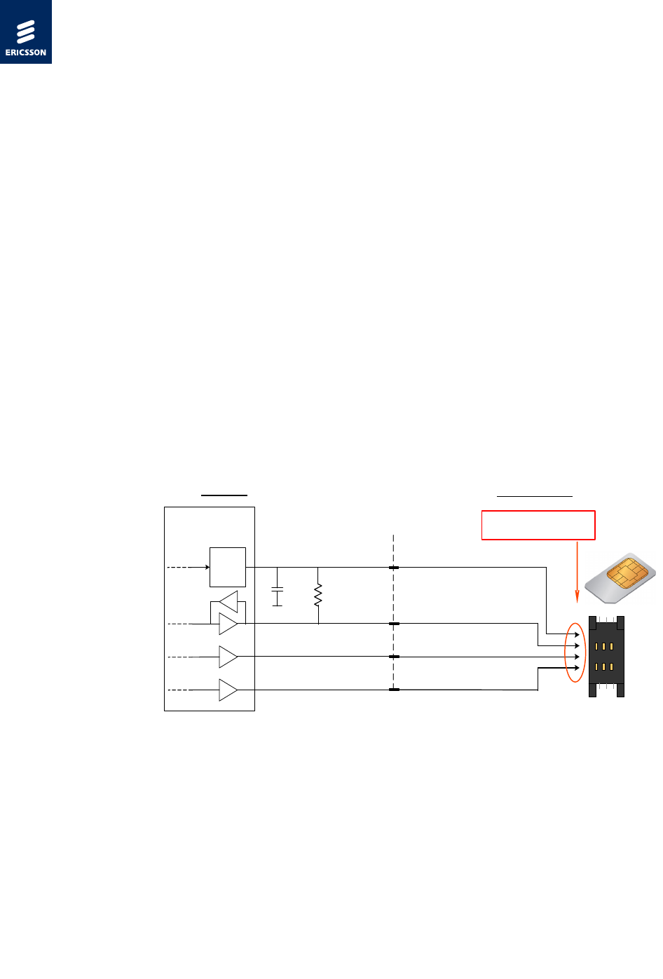
4.3.7 UICC Interface
The UICC interfaces consist of the following signals:
• UIM Power
• UIM Data
• UIM Clock
• UIM Reset
• UIM SIMOFF
The picture below illustrates the UICC (SIM) interface.
Note: The UICC interface should be ESD protected on the host side.
10kOhm
UIM_PWR
UIM_CLK
UIM_RST
UIM_DATA
LGA PADS
LDO
1.8/3V
SIM
Interface
1µF
Place ESD protection
close to SIM card holder
Module Host Device
Figure 15, UICC interface
4.3.7.1 UIM _PWR
Function:
UIM Power
Description:
1.8 V or 3 V power supply to the UICC
Signal Name: UIM_PW R [Module⇒UICC]
If not used: Required
Integrator's Guide - C5621 / C33
2/1553-KRD 131 24 Uen Rev D 2011-11-15
Ericsson AB 2011
43 (72)
Ericsson Confidential
LVTTL: N/A
Details:
The UIM_PWR signal is the Ericsson Mobile Broadband
Module power supply to the UICC. The Ericsson Mobile
Broadband Module supports UICC of Class B and C.
The signal details shall be according to [14].
Note: Only the UICC reader may be connected to UIM_PWR. The UIM_PWR signal
should not be fitted with decoupling capacitors in the host design.
Table 8, UIM_PWR Electrical Characteristics
Parameter Condition Min T ype Max Unit
UIM_PW R 1.8 V mode 1.67 1.8 1.98 V
3 V mode 2.8 2.85 2.9 V
4.3.7.2 UIM_DATA
Function: UIM Data
Description:
Single-ended data signal
Signal Name: UIM_DAT A [Module⇔UICC]
If not used: Required
LVTTL: N/A
Details: The Ericsson Mobile Broadband Module provides this data
signal interface to the host mounted UICC. A 10 kOhm pull-
up resistor to UIM_PWR is mounted on the module.
The signal details shall be according to [14].
Integrator's Guide - C5621 / C33
2/1553-KRD 131 24 Uen Rev D 2011-11-15
Ericsson AB 2011
44 (72)
Ericsson Confidential
Table 9, UIM_DATA Electrical Characteristics:
Parameter Condition Min T ype Max Unit
UIM_DATA
Input low level 0.2 x
UIM_PW R V
Input high level 0.7 x
UIM_PW R V
Output low level 0 0.3 V
Output high level U IM_PW R
-0.3 U IM_PW R V
4.3.7.3 UIM_CLK
Function:
UIM Clock
Description:
Single-ended clock signal
Signal Name: UIM_CLK [Module⇒UICC]
If not used: Required
LVTTL: N/A
Details: The Ericsson Mobile Broadband Module provides this clock
signal interface to the host mounted UICC. The signal details
shall be according to [14].
Table 10, UIM_CLK Electrical Characteristics
Parameter Condition Min T ype Max Unit
UIM_CLK
1.8 V mode, low
level 0 0.2 V
1.8 V mode, high
level 1.6 UIM_PW R V
3 V mode, low level 0 0.35 V
3 V mode, high
level 2.4 UIM_PW R V
4.3.7.4 UIM_RST
Function:
UIM Reset
Description:
Reset signal to the UICC

Integrator's Guide - C5621 / C33
2/1553-KRD 131 24 Uen Rev D 2011-11-15
Ericsson AB 2011
45 (72)
Ericsson Confidential
Signal Name: UIM_RST [Module⇒UICC]
If not used: Required
LVTTL: N/A
Details: The Ericsson Mobile Broadband Module provides this reset
signal interface to the host mounted UICC. The signal details
shall be according to [14].
Table 11, UIM_RST Electrical Characteristics
Parameter Condition Min T ype Max Unit
UIM_RST
1.8 V mode, low
level 0 0.2 V
1.8 V mode, high
level 1.6 UIM_PW R V
3 V mode, low level 0 0.35 V
3 V mode, high
level 2.4 UIM_PW R V
4.3.7.5 UIM_SIMOFF_N (For Future Use)
Function: UICC interface disable
Description: Active low UICC interface disable
Signal Name: UIM_SIMOFF_N [UICC⇒Module]
Table 12, UIM_SIMOFF_N Electrical Characteristics
Parameter Condition Min T ype Max Unit
UIM_SIMOFF_N 1.8 V mode 1.67 1.8 1.98 V
4.3.8 PCM 0 & 1 Interface
The module is hardware prepared to support digital voice interface between
the module and the host. PCM 0 & 1 are intended for that purpose. For
C5621/C33 module configuration, this interface is not enabled. Hence, the
signals corresponding to PCM 0 /1 interface shall be pulled-low or tied to
GND. Refer to Table 3 for pin details.

Integrator's Guide - C5621 / C33
2/1553-KRD 131 24 Uen Rev D 2011-11-15
Ericsson AB 2011
46 (72)
Ericsson Confidential
4.3.9 RF interface
4.3.9.1 RF_MAIN
Function: Main antenna port for E-GSM and WCDMA
Description: 50Ω antenna interface used for main RF branch
Signal name: RF_MAIN
Direction: Module antenna system
If not used: Required
LVTTL: N/A
Details: No DC protection implemented on this interface.
4.3.9.2 RF_DIV
Function: Antenna port for WCDMA diversity
Description: 50Ω antenna interface used for receive diversity branch
Signal name: RF_DIV
Direction: Antenna system => module
If not used: Required
LVTTL: N/A
Details: No DC protection implemented on this interface.
4.3.9.3 RF_GPS
Function: Antenna port for GPS interface
Description: 50Ω antenna interface used for GPS
Signal name: RF_GPS
Direction: Antenna system => module
If not used: Leave open
LVTTL: N/A
Details:
Maximum DC rating on this interface is 3V @ 25 +/- 2
degrees C.
Integrator's Guide - C5621 / C33
2/1553-KRD 131 24 Uen Rev D 2011-11-15
Ericsson AB 2011
47 (72)
Ericsson Confidential
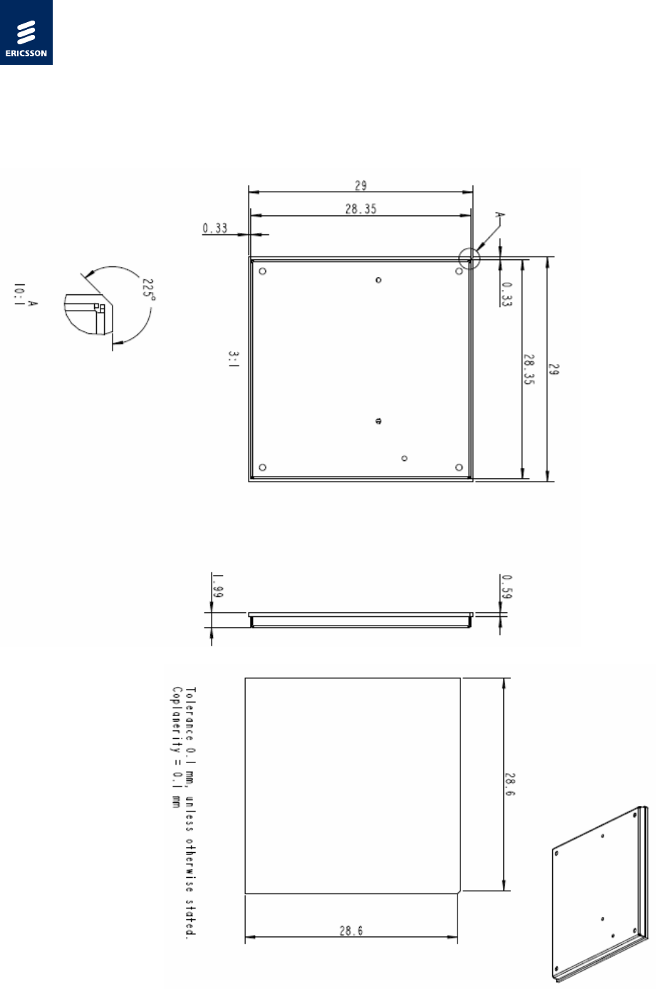
5 Mechanical Dimension
Figure 16, Physical Dimension (All dimensions in mm)

Integrator's Guide - C5621 / C33
2/1553-KRD 131 24 Uen Rev D 2011-11-15
Ericsson AB 2011
48 (72)
Ericsson Confidential
6 Routing guidelines
C5621 / C33 Mobile Broadband module is an LGA subassembly, soldered to
the host board, and shares GND plane with the host platform, it is essential
that the host board layout follows the recommendation given in this chapter to
get the best performance out of the module.
Some of the recommendations provided in this chapter are general PCB
design guideline that may be referred from standard texts concerning the
subject.
6.1 Recommended PCB Footprint
The solder lands of the host PCB should be a mirror image of the 277
Ø ≥0.63 mm solder lands on the component and preferably not routed on the
outer Cu-layer. The pitch is 1.27 mm. Via-in-pad should be Cu-filled (i.e. solid
Cu-microvia).
To improve flux outgassing during reflow, the Solder Mask Opening (SMO) is
recommended to extend 50 µm outside the package outline on all four sides.
Figure 17, Ø 0.63 mm solder lands with one large solder mask opening
extending at least 50 μm outside the package outline on all four
sides
Host PCB Solder Mask
Solder Mask Opening
29.2 mm
29.2 mm

Integrator's Guide - C5621 / C33
2/1553-KRD 131 24 Uen Rev D 2011-11-15
Ericsson AB 2011
49 (72)
Ericsson Confidential
If solder mask is used on the mother PCB underneath the C5621/C33, it
should be NSMD design with SMO of Ø ≥0.73 mm.
Figure 18, Ø 0.63 mm NSMD solder lands, SMO Ø ≥0.73 mm
6.2 Digital I/O routing
Keep all trace lengths as short as possible
Use stripline structure for signals with high frequency content (on the
module, all 1.8V I/O signals have a rise/fall time of ~1ns, and should
therefore be routed as striplines, since they all are high bandwidth
signals)
Treat all critical (high bandwidth) signals as current loops, and make
sure that they have a return path. This means that you should refrain
from routing any signals over non-continuous power or ground planes,
because this causes interruptions in the impedance and results in
reflections, and might also increase EMI emissions.
Traces routed on adjacent layers should be oriented perpendicular
towards each other; this will reduce risk for crosstalk.
Impedance matching must be maintained to avoid overshoot,
undershoot and ringing. Otherwise, radiated emissions increases.
If nothing else is stated, digital signals should be routed with an
impedance of 50-70 Ohm relative GND.
NSMD Solder lands
Host PCB Solder Mask
Integrator's Guide - C5621 / C33
2/1553-KRD 131 24 Uen Rev D 2011-11-15
Ericsson AB 2011
50 (72)
Ericsson Confidential
6.2.1 Clock Routing
Must be routed with a controlled impedance (50-60 Ohm)
Should not be routed over a discontinuous GND plane
Keep clock traces as short as possible
Place serial termination close to transmitter output
Crosstalk:
o Crosstalk falls off with the square of the distance, therefore
adequate spacing is a good method in reducing crosstalk
o As a rule of thumb, 3xH can be used for all clock signals:
Figure 19, Spacing rule
Involved signals:
o SYSCLK
o RTC_CLK
o UIM_CLK
6.2.2 USB Routing
Traces should be routed as a differential pair, matched in length.
Differential Impedance between the traces shall be 90 Ohm
Involved signals:
o USB_DP
o USB_DM
H
3xH
Reference plane
Aggressor Victim

Integrator's Guide - C5621 / C33
2/1553-KRD 131 24 Uen Rev D 2011-11-15
Ericsson AB 2011
51 (72)
Ericsson Confidential
6.3 Power Routing
6.3.1 VBAT Routing
The VBAT pads should have a direct, low impedance connection to a
battery
The decoupling should be placed close to VBAT pads
VBAT net shall be designed such that the supply voltage to the module is
always within its operating range even at the maximum current
consumption (worst case being 2G transmit operation). Refer to chapter
4.3.3.1 for details
6.3.2 GND
On the layers where a power plane is implemented, a cut-out creating a local
GND plane should be implemented. The local plane should be connected to
the complete GND planes with as many vias as possible; this will increase the
thermal coupling.
6.4 RF Routing
RF signals must have a controlled impedance of 50 Ohm
The signals should be directly connected to respective antennas / antenna
connectors
It is important to isolate the RF-lines from any unwanted signal or noise.
RF stripline is a good choice for realization of RF-lines since it provides
good shielding from both radiated and conducted noise. Care must also be
taken to isolate main/diversity/GPS traces with regards to each other.
Via fence around the stripline, creating an embedded RF cage in the PCB,
will improve isolation. Care shall be taken while calculating trace
impedance since via fence placed very close to the RF striplines, may
lower the impedance somewhat.
Via stub should be eliminated or minimized

Integrator's Guide - C5621 / C33
2/1553-KRD 131 24 Uen Rev D 2011-11-15
Ericsson AB 2011
52 (72)
Ericsson Confidential
7 Production Guideline
7.1 Package type
C5621 / C33 module has ENIG bottom terminations with a LGA design; no
solder mask is present at the underside of the package.
Figure 20, Top view of C5621/C33
7.2 Floor life and dry storage
The CE module should be stored in a dry pack and handled according to
IPC/JEDEC J-STD-033B.1, MSL 3 with bake at:
• 125 °C, when supplied on JEDEC tray
• 40 °C ≤5% RH when supplied on 44 mm tape and reel
7.3 Screen stencil design
Material: Stainless steel
Thickness: 0.1 mm (~4 mil)
Aperture size: Ø 0.63 mm (277x)
All solder paste deposits should be centered on the PCB.
7.4 Assembly
Pick-up position should be centered on the package topside.
Nozzle Ø: 10-20 mm

Integrator's Guide - C5621 / C33
2/1553-KRD 131 24 Uen Rev D 2011-11-15
Ericsson AB 2011
53 (72)
Ericsson Confidential
7.5 Reflow soldering
Forced convection soldering in air or N2 can be used.
Reflow profile shall be with the stated limits in IPC/JEDEC J-STD-020D.1.
The classification temperature (Tc) is 250 °C1.
1 The temperature value is according to the requirements stated in Tabl e 4-2 IPC/JEDE C J-STD-020D.1.
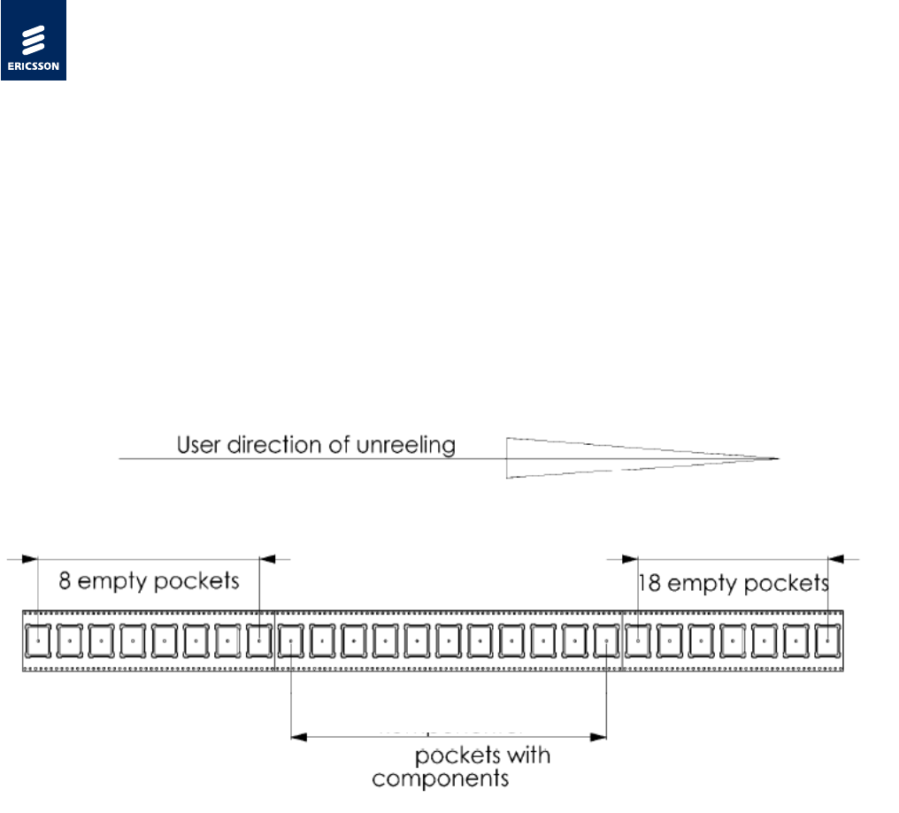
Integrator's Guide - C5621 / C33
2/1553-KRD 131 24 Uen Rev D 2011-11-15
Ericsson AB 2011
54 (72)
Ericsson Confidential
8 Packaging – Tape and Reel Information
C5621/C33 modules are shipped as tape reels.
Each reel has 724 modules placed into the carrier tape and sealed with the
cover tape. There will be 8 empty pockets as trailer and 18 empty pockets as
leader in each reel.
Figure 21, Reel Direction
724
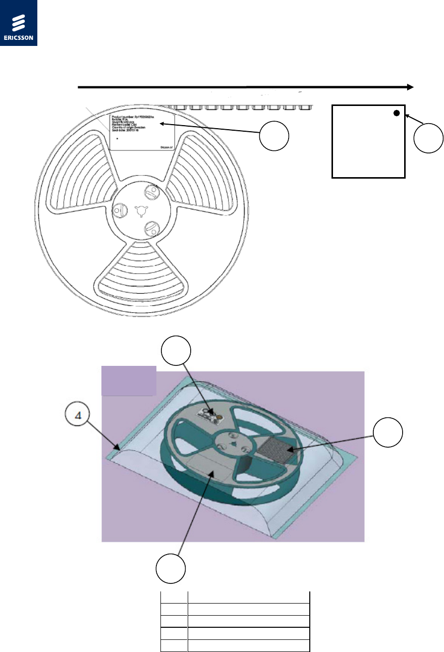
Integrator's Guide - C5621 / C33
2/1553-KRD 131 24 Uen Rev D 2011-11-15
Ericsson AB 2011
55 (72)
Ericsson Confidential
1
Label
2
Humi dity Indicator
3
Desiccant
4
Shielding Bag
5
Module Orientation Mark
Figure 22, Tape Reel Details
User direction of unreeling
1
C5621/C33
Module
5
2
1
3

Integrator's Guide - C5621 / C33
2/1553-KRD 131 24 Uen Rev D 2011-11-15
Ericsson AB 2011
56 (72)
Ericsson Confidential
9 SW integration
9.1 Driver and Application Architecture
9.1.1 Windows XP and Vista Architecture
The driver and application architecture for XP and Vista is depicted in Figure
23.
The drivers are based on standard USB functionality. The Mobile Broadband
Module appears as the following devices when examined in Windows Device
Manager:
Device Name
Function
Mobile Broadband Device Management
This port can be used by an application
to control and obtain status from the
Mobile Broadband Module. Port type
WDM
Mobile Broadband Network Adapter
(NDIS)
NDIS i nterface over which Ethernet
communication can be established.
Appears to Windows as a network
adapter. Port type Ethernet
Mobile Broadband GPS Interface
GPS COM port which streams out
NMEA. Port type ACM
SIM Card Reader (SC)
PC-Smartcard interface. Port type WDM
Wireless Modem
Modem device which may be used for
legacy Dial-Up Networking connection.
Port type ACM.
On top of the drivers is an application, WMCore, running as background
service. The service is started automatically at Windows startup and can be
used to change the state of the Mobile Broadband Module without end-user
interaction also prior to Windows login.
The WMCore service provides a number of functions to control the module
and retrieve information about the module and its states. The functions are
accessible through the Ericsson Mobile Broadband C++ API, see [5]. The
service is also used by Ericsson’s Wireless Manager.
Integrator's Guide - C5621 / C33
2/1553-KRD 131 24 Uen Rev D 2011-11-15
Ericsson AB 2011
57 (72)
Ericsson Confidential
NME
A
F3507g / F3607gw
Bus Driver
WMCore
GPS
SC
Modem
Modem
Mgmt
Windows 7
Network
subsystem
Wireless Manager 6.0
C++ API
Drivers
USBHW
ETH
Mobile Broadband
Module
ACM
Bus Driver
Service
GPS
SC
Modem
Modem
Mgmt
NDIS
Miniport
Windows
Network
subsystem
Wireless Manager
Ericsson C++ API
Drivers
USBHW Applications
Control
WDM
ACM
ACM
WDM
ETH
AT
Figure 23, Windows XP/Vista driver architecture
9.1.2 Windows 7 Architecture
The driver and application architecture for Windows 7 is depicted in Figure 24.
The Mobile Broadband Module drivers are based on standard USB
functionality. The Windows 7 drivers support the native Windows 7 Mobile
Broadband API, resulting in a different architecture compared to Windows XP
and Vista, as visualized in Figure 24. The GPS driver also implements support
for Microsoft’s sensor class. The devices seen in the Windows 7 Device
Manager are as follows:
Device Name
Function
Mobile Broadband Device Management
This port can be used by an application
to control and obtain status from the
Mobile Broadband Module. Port type
WDM
Mobile Broadband Network Adapter
(NDIS 6.2 0)
Implements support for the Windows 7
Mobile Broadband API. Appears to
Windows as a WWAN adapter. Port type
Ethernet and ACM
Mobile Broadband GPS Interface
GPS port that supports the Windows 7
sensor class but can also be used as a
Integrator's Guide - C5621 / C33
2/1553-KRD 131 24 Uen Rev D 2011-11-15
Ericsson AB 2011
58 (72)
Ericsson Confidential
COM interface. Port type ACM
SIM Card Reader (SC)
PC-Smartcard interface. Port type WDM
Wireless Modem
Modem device which may be used for
legacy Dial-Up Networking connection.
Port type ACM.
On top of the Windows 7 drivers is located a smaller WMCore service, which
handles module functionality not handled by the Microsoft’s Mobile Broadband
API. The functionality handled by the service can be reached through the
Ericsson Mobile Broadband C++ API.
The Wireless Manager works the same way in Windows 7 as it does in
Windows XP and Vista. A port layer makes sure that Wireless Manager uses
Microsoft’s Mobile Broadband API as much as possible and uses the WMCore
service only for functionalities not supported by the Mobile Broadband API.
This ensures that Wireless Manager is synchronized with any other
functionality using the Mobile Broadband API, including the native connection
manager in Windows 7.
OID
NMEA
ACM
F3507g / F3607gw
Bus Driver
GPS
SC
Modem
Mgmt
DriversUSBHW Applications
IP
Mobile Broadband
Module
ACM
Bus Driver
Service
GPS
SC
Modem
Mgmt
NDIS
6.20
Miniport
Windows 7 Mobile Broadband Core
Wireless Manager
DriversUSBHW
Control
WDM
ACM
WDM
ETH
AT
Sensor
Windows 7 Mobile Broadband API
Windows 7
Mobile Broadband
User Interface
Ericsson
C++ API Port Layer
Figure 24, Windows 7 driver and application architecture
Integrator's Guide - C5621 / C33
2/1553-KRD 131 24 Uen Rev D 2011-11-15
Ericsson AB 2011
59 (72)
Ericsson Confidential
9.1.3 Linux driver architecture
Ericsson is a part of the Linux community to continuously improve the support
in GNU/Linux for Ericsson Mobile Broadband Modules, please see [7] for more
information.
The module firmware provides WDM (Wireless Mobile Communications
Device Management) interfaces for device management and AC M (Abstract
Control Module) interfaces for control and data traffic. The module exposes
ACM ports, which can be used for GPS, Connection Manager and SMS. WDM
and ACM are both based on CDC (Communication Device Class). Control is
handled by AT commands according to the V.25 standard. The network
connection uses USBnet architecture as base with support from CDC-NC M.
The module supports DUN using PPP on the ACM interface.
Note: Kernel modifications may be needed to support customer requested VID/PID
customizations, check with your Linux distributor.
Network Manager and GPS functionality is provided by user space
applications.
For more information please refer to [8]
Figure 25, Linux driver architecture
Host USB Hardware
USB Core
USBnet
ACM
WDM
Hardware
Kernel
Legend
GPS
Control
Kernel-space
User-space
Network
Manager
Module
CDC-NCM

Integrator's Guide - C5621 / C33
2/1553-KRD 131 24 Uen Rev D 2011-11-15
Ericsson AB 2011
60 (72)
Ericsson Confidential
9.2 Connection Profile List
In Windows XP and Vista, the WMCore service includes a list with connection
profiles which can be used by connection managers when setting up
connections. The profile list contains a list of default network operator APN
which is automatically selected by the connection manager depending on the
detected UICC card. The matching between APN and UICC card is done
based on the MCC and MNC (2 or 3 digit). In Windows 7 the list of profiles is
part of the WWAN adapter and is accessed and handled through the Windows
7 Mobile Broadband API as specified by Microsoft.
Wireless Manager utilizes the profile list in the WMCore service in Windows
XP and Vista. In Windows 7, Wireless Manager carries the profile list itself to
facilitate updates of the list without requiring a driver update. Updates of the
connection profile list can be made by using a Connection Profile Updater, for
more information, see [6]. The connection profile updater updates the profile
list in WMCore in XP and Vista and the profile list carried by Wireless Manager
in Windows 7.
9.3 Ericsson Mobile Broadband C++ API
The Ericsson Mobile Broadband C++ API (the C++ API) is part of the Ericsson
Mobile Broadband Software Development Kit (SDK), which is available for
integration of mobile broadband modules. The C++ API can be used as an
extension to the Mobile Broadband API in Windows 7 to access functionality
not supported in the Mobile Broadband API. In Windows XP and Vista, the
C++ API covers the entire Mobile Broadband API as well as the extensions.
The C++ API is backward compatible. The C++ API supports multi-process
and multi-thread access. By using the C++ API, application development
becomes easier and more efficient since high-level interfaces can be used.
The C++ API also leverages on functionality provided by the WMCore service,
which includes:
• Module state and concurrency handling
• Windows Auto-connect and pre-logon connect
• Always-on functionality
• Automatic state transitions after Sleep(S3) and WWAN disable
• GPS configuration
• Internet account (APN) configuration
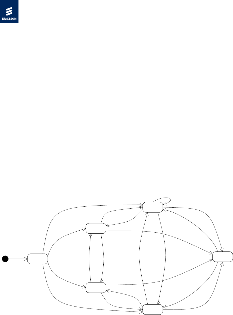
Integrator's Guide - C5621 / C33
2/1553-KRD 131 24 Uen Rev D 2011-11-15
Ericsson AB 2011
61 (72)
Ericsson Confidential
9.4 State machine
The state machine focuses on the main states of the module; states of the
mobile radio (Radio On/Off) and the GPS radio (GPS On/Off). The transitions
in the state machine that require the Software (radio) and GPS to be enabled
can be made using the WMCore service (recommended) or AT commands
directly. In Windows 7, several of the transitions are caused by the WW AN
(Network) driver.
The transition between HW Off and states where the radio is on can be made
automatically by the module without including any host software, see chapter
2.2.
The module supports a SW Off (D3 hot) state where most functionality is
turned off in the mobile broadband module. The main intention with the state is
to prepare the module to be powered off. Among other things is the SIM card
turned off. In the SW Off state it is possible to turn the module back on again
using AT commands (AT+CFUN). When the module is turned on the SIM card
is reset and all functionality of the mobile broadband module is turned on
again.
Additionally, the module supports a separate HW control of GPS Off, see
chapter 0. This feature is not depicted in Figure 26.
HW Off
(D3)
Radio Off
GPS Off
Radio Off
GPS On
Radio On
GPS On
Radio On
GPS Off
Module Powered
(Hardware && Software
Enabled && GPS Disabled)
Module Powered
(Hardware && Software
Enabled && GPS Enabled)
Module Powered
(Software Disabled &&
Hardware Enabled && GPS
Enabled)
Module Powered
( (Hardware || Software
Disabled) && (Hardware ||
GPS Disabled) )
GPS Enable
GPS Disable
GPS Enable &&
HW Enabled
HW Disable ||
GPS Disable
Hardware &&
Software Enabled
Hardware ||
Software Disabled
Software Enabled
Software Disabled
SW Off
(D3 Hot)
HW Disable ||
SW Disable
Software Off
Software Off
Software Off
Software Off
Software On
(Software &&
Hardware Enabled)
Software On
(Software ||
Hardware Disabled)
Figure 26, State machine for C5621 (Same applicable for C33 - Excluding
GPS events)

Integrator's Guide - C5621 / C33
2/1553-KRD 131 24 Uen Rev D 2011-11-15
Ericsson AB 2011
62 (72)
Ericsson Confidential
9.5 Service Windows Registry Keys
The Ericsson WMCore service uses Windows Registry Keys to control the
module behavior during OS power-state changes. Windows TCP/IP settings
can also be optimized automatically when installing the drivers. When using
the Ericsson Mobile Broadband C++ API there is no need to manually control
the registry settings, however, integrators opting for using the module without
the API could use these. The register settings are used to control the following
features:
• Always On (OS power event behavior)
• Auto connect
• Auto radio enable
• TCP/IP optimization for WWAN devices.
Note: The registry settings are defined within the definition of the WMCore service.
The registry settings definition and function can be changed or removed
without prior notice.
9.5.1 Module state
The following parameters control the module function state during OS power
event changes. They are used to synchronize the module state to OS state.
Please refer to the AT Command Manual [4] for details on CFUN state.
The registry keys are set during the driver and WMCore installation.
Search path:
[HKEY_L OCA L_MA CHINE\SOFTWARE\WMCore]
(32bit installations)
[HKEY_LOCAL_MACHINE\S OF TW A RE\Wow6432Node\WMCore]
(64bit installations)
Table 13 Module state settings
Name Type Description
LastKnownRadioState REG_DWORD CFUN value to set after boot / reboot.
ShutdownCFUN REG_DWORD CFUN value to set before shutdown /
reboot.
KeepRadioStateDuringSleep
REG_DWORD 0: Do not keep current radio state
1: Keep radio state when entering sleep

Integrator's Guide - C5621 / C33
2/1553-KRD 131 24 Uen Rev D 2011-11-15
Ericsson AB 2011
63 (72)
Ericsson Confidential
Table 14 Connection state settings
Name T ype Description
AllowAutoConnectAfterSleep
REG_DWORD
0: Never autoconnect after sleep, regardless of
previous state
1: Allow reconnection, if previously connected.
AutoConnectStartup REG_DWORD 0: Do not automatically connect after boot.
1: Automatically connect after boot.
DisableAutoConnect REG_DWORD 0: Does nothing
1: Never autoconnect
9.5.2 TCP/IP Configuration
As part of installation in Windows XP, the following registry settings are made
in order to optimize the throughput for WWAN devices.
[HKEY_LOCAL_MACHINE\SYSTEM\Current ControlSet\Services\Tc pip\Paramet ers]
Table 15 TCP/IP Optimization
Name T ype Value
TcpWindowSize REG_DWORD 0x40290
Tcp1323Opts REG_DWORD 0x1
Note: Setting Tcp1323Opts="0x3" and thus enabling Timestamp might help in some
cases where there is increased packet loss. However, generally better
throughput is achieved with Tcp1323Opts="0x1", since Timestamps add 12
bytes to the header of each IP packet.

Integrator's Guide - C5621 / C33
2/1553-KRD 131 24 Uen Rev D 2011-11-15
Ericsson AB 2011
64 (72)
Ericsson Confidential
10 Firmware Updates
Within a single model of the Mobile Broadband Module, different firmware
configuration may be introduced for mainly two reasons:
1. A firmware configuration may be accepted by some mobile operators
whereas other may require further changes to be made. This will result
in that two or more versions have to be available at the same time.
2. Updated firmware configurations with added features and error
corrections are created as maintenance releases, which can be
supplied to the end-user for improved performance.
The first of these two reasons for different firmware configurations has
traditionally resulted in multiple SKUs of the Mobile Broadband Module. The
situation is improved now as the module will be able to change firmware
configuration automatically, see chapter 10.1.
The second reason for different firmware configurations results in that the
updated firmware is distributed to the end-user as a firmware updater
application to be run on the host device.
10.1 Network Dependent Firmware Updates
The Mobile Broadband module has the capability of storing several different
firmware configurations in the persistent on-board flash memory. A database
containing information about all operators that have approved a specific
firmware configuration is stored in the module. When a new firmware
configuration is released the database will be updated. During module
manufacturing the latest database available is stored in the module memory
together with the valid released and approved firmware configurations.
During startup, the module will use the UICC card to identify the network
operator that is currently used. The module can, based on this information
select to use a different firmware configuration.
The host software can supply the end user with information regarding the
updates as well as provide interfaces for 3rd party applications to implement
own support for showing update information.
For more information regarding Network dependent firmware updates, see [9].

Integrator's Guide - C5621 / C33
2/1553-KRD 131 24 Uen Rev D 2011-11-15
Ericsson AB 2011
65 (72)
Ericsson Confidential
11 Terminology and abbreviations
2G Generic term for the second generation of cellular
networks. GSM is a 2G network.
3G Generic term for the third generation of cellular networks
such as UMTS
3GPP The 3rd Generation Partnership Project
AC M Abstract Control Model USB communications device
class
AC P I Advanced Configuration and Power Interface
AP N Access Point Name
AR P Antenna Reference Point
CDC USB communications device class
Cu Copper
DRX Discontinuous reception
ECN Engineering Change Notice
EDGE Enhanced Data rates for GSM Evolution
ENIG Electroless Nickel/Immersion Gold
ESD Electro-Static Discharge
GPRS General Packet Radio Service
GPS Global Positioning System
GSM Global System for Mobile Communications
GSMA GSM Association
HSPA High Speed Packet Access
LED Light-Emitting Diode
LGA Land Grid Array
LTO Long Term Orbits (Internet Assisted GPS)
MSL Moisture Sensitivity Level

Integrator's Guide - C5621 / C33
2/1553-KRD 131 24 Uen Rev D 2011-11-15
Ericsson AB 2011
66 (72)
Ericsson Confidential
N2 Nitrogen
NCM Network Control Model USB communications device
class
NDIS Network Driver Interface Specification
NSMD Non Solder Mask Defined
PCB Printed Circuit Board
PC OEM Personal Computer Original Equipment Manufacturer
PGPS Predicted GPS
PLMN Public Land Mobile Network
RF Radio Frequency
RH Relative Humidity
Rx Receive
S AR Specific Absorption Rate
SC Smart Card
SIM Subscriber Identity Module
SIP System In Package
SKU Stock-Keeping Unit
SMO Solder Mask Opening
SUPL Secure User PLane (Network Assisted GPS)
Tx
Transmit
UICC Universal Integrated Circuit Card
UMTS Universal Mobile Telecommunications System
USIM Universal Subscriber Identity Module
USB Universal Serial Bus
WCDMA Wideband Code Division Multiple Access
WDM Wireless Mobile Communications Device Management
USB communications device class
Wo W Wake on Wireless

Integrator's Guide - C5621 / C33
2/1553-KRD 131 24 Uen Rev D 2011-11-15
Ericsson AB 2011
67 (72)
Ericsson Confidential
WWAN Wireless Wide Area Network

Integrator's Guide - C5621 / C33
2/1553-KRD 131 24 Uen Rev D 2011-11-15
Ericsson AB 2011
68 (72)
Ericsson Confidential
12 References
[1] C5621gw Technical Description
1/1550-KRD 131 24
Ericsson AB
[2] 3G in Notebooks Guidelines version 4
Copyright © 2007 GSM Association
[3] Universal Serial Bus Specification 2.0
Copyright © 2000, Compaq Computer Corporation, Hewlett-Packard
Company, Intel Corporation, Lucent Technologies Inc, Microsoft
Corporation, NEC Corporation, Koninklijke Philips Electronics N.V. All
rights reserved.
[4] AT Command Manual
3/1553-KRD 131 15+
Ericsson AB
[5] Ericsson Mobile Broadband SDK
1/1550-CXP 901 4397/1
Ericsson AB
[6] Connection Profile Updater
1553-CXC 172 8313/1
Ericsson AB
[7] MBM Linux Support
1/102 72-HRC 105 042
Ericsson AB
[8] MBM Linux Wiki, http://mbm.sourceforge.net
[9] Network Dependent Firmware Upgrades
1/1550-KRD 131 18+
Ericsson AB
[10] Antenna Performance Guideline
1/1553-FAF 901 658/1
Ericsson AB
[11] Evaluating Compliance with FCC Guidelines for Human Exposure to
Radiofrequency Electromagnetic Fields
OET Bulletin 65 Supplement C (2001-01)
[12] Assessment Of Electronic And Electrical Equipment Related To
Human Exposure Restrictions For Electromagnetic Fields (0 Hz - 300
GHz)
EN 62311:2008
[13] Electronic Industries Association, "EIA Standard RS-232-C Interface
Between Data Terminal Equipment and Data Communication

Integrator's Guide - C5621 / C33
2/1553-KRD 131 24 Uen Rev D 2011-11-15
Ericsson AB 2011
69 (72)
Ericsson Confidential
Equipment Employing Serial Data Interchange", August 1969,
reprinted in Telebyte Technology Data Communication Library,
Greenlawn NY, 1985, no ISBN
[14] Smartcards, UICC-Terminal Interface; Physical and logical
Characteristics, ETSI TS 102 221
[15] Wake on Wireless
2/198 10-FAF 901 658/1
Ericsson AB

Integrator's Guide - C5621 / C33
2/1553-KRD 131 24 Uen Rev D 2011-11-15
Ericsson AB 2011
70 (72)
Ericsson Confidential
13 Annex
13.1 Test Setup for Measuring Host-Generated Noise
For a module integrated in host the total noise density level ( tot
N) seen at the
GPS receiver can be expressed as the sum of different contributions.
• Thermal Noise – Generated within the GPS receiver
• External Noise – Generated by the laptop
• WW AN Noise – Generated by the WWAN transmitter
All of these noise sources are uncorrelated and will add up to a total noise
density tot
N at the auxiliary Antenna Reference Port (ARP), according to
Equation 1.
Equation 1 Total noise level [W/Hz]
wwanextttot NNNN ++=
The thermal noise density generated by the GPS receiver itself is equal
to kTFNt=, where
kT
is -174 dBm/Hz at room temperature and
F
is the
noise figure, typically 3.5 dB. The noise density generated by the GPS
receiver is then calculated to -170.5 dBm/Hz=-116.5 dBm/MHz.
The thermal noise is the critical contribution and will set the limit for the GPS
performance.
Assume that the WWAN radio is disabled, then wwan
N
can be set to zero and
therefore neglected in the further analysis.
To minimize the impact of the noise generated outside the GPS receiver a
noise margin
M
is introduced, according to Figure 27.
Ntot
Nt
∆
Next
M
Figure 27, Definition of Noise Margin
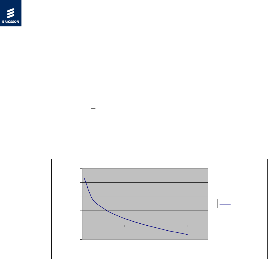
Integrator's Guide - C5621 / C33
2/1553-KRD 131 24 Uen Rev D 2011-11-15
Ericsson AB 2011
71 (72)
Ericsson Confidential
The external noise must be lower than the thermal noise to conserve the GPS
performance. The main question is how much lower?
The noise margin can be expressed as a function of the noise degradation as
in Equation 2.
Equation 2 Noise Margin [dB]
−
=∆
110
1
log10
10
M
Equation 2 then plotted in Figure 28 Noise Margin as a function
of degradation
as function of the degradation.
-5,0
0,0
5,0
10,0
15,0
20,0
0,0 1,0 2,0 3,0 4,0 5,0 6,0
Degradation [dB]
Margin [dB]
Noise Margin
Figure 28 Noise Margin as a function of degradation
It can be seen that if the margin is set to zero, then the degradation is 3 dB. A
consequence of this is that the noise generated by the host device must be
substantially lower than the internal noise generated by the receiver it self.
So if the overall performance shall be conserved we can assume that the total
noise level shall be degraded only 1 dB. This assumption gives,
according to Figure 28 Noise Margin as a function of degradation
, that the margin must be 6 dB and therefore the noise generated by the host
device at ARP must be less than -176.5 dBm/Hz=-116.5 dBm/MHz.
13.1.1 Test Setup
The test setup for measuring host-generated noise at ARP consists of two
host devices:

Integrator's Guide - C5621 / C33
2/1553-KRD 131 24 Uen Rev D 2011-11-15
Ericsson AB 2011
72 (72)
Ericsson Confidential
• Host Device 1 (HD1) is used to control the GPS and measure the 0
/NC
value.
• Host Device 2 (HD2) is the host device to be investigated, also known as
the Device Under Test (DUT). A coaxial cable is connected from HD2
auxiliary antenna to HD1 auxiliary antenna reference port (ARP).
The test is made in two steps:
1 A reference measurement is done with HD2 turned OFF. The signal
strength from all satellites is documented.
2 Then HD2 is turned ON, and a second measurement is performed. The
signal strength from all satellites is documented.
The 0
/NC difference for each satellite is caused by noise added by HD2.
This measurement gives valid estimates if the signal strength from the
satellites can be assumed to be constant.
Equation 3 Relation between 0
/NC and
rx
P
totrx
NP
N
C−=
0
Assume that
rx
P
is constant during the measurement period, then C/No is only
dependent of tot
N
, according to Equation 3.
Doing this test with open sky and good signal conditions makes it possible to
estimate the increased noise density caused by HD2.