Wuerth Elektronik eiSos and Co KG AMB2524 AMB2524 User Manual Testreport ETS 300 335
AMBER Wireless GmbH AMB2524 Testreport ETS 300 335
UserManual.wiki
>
Wuerth Elektronik eiSos and Co KG
>
AMB2524 User Manual
Users Manual
Navigation menu
Upload a User Manual
Namespaces
Wiki Guide
HTML
PDF
Info
Views
User Manual
Discussion / Help
Navigation
![AMB8420_2524_2561_MA_V4_2 Page 7 of 61 Date: 12/2017 3 Electrical parameters 3.1 Input voltage The input voltage of the module ranges from 2.7 to 3.6 V. In order to ensure a constant processor frequency (and UART clock rate) over the entire voltage range, the clock rate is continuously readjusted on the basis of the available watch crystal. Voltage changes during the reception or output over the serial interface can result in a change of the clock rate between two characters. Caution: A clean supply voltage is needed for the module to function correctly. Using a 100 µF blocking capacitor close to the VCC pin is a useful measure (especially when using RS232 converters or clocked DC-DC converters). 3.2 Power consumption 3.2.1 AMB8420 See data sheet [4]. 3.2.2 AMB2524 See data sheet [5]. Caution: To minimize power consumption in Sleep Mode, the input signals of the module (/CONFIG, SLEEP, TRX_DISABLE und /DATA_REQUEST) must be set to the levels defined in Table 1. Open (floating) pins result in increased power consumption. 4 Dimensions and weight See data sheets [4] and [5].](https://usermanual.wiki/Wuerth-Elektronik-eiSos-and-Co-KG/AMB2524/User-Guide-3737675-Page-8.png)
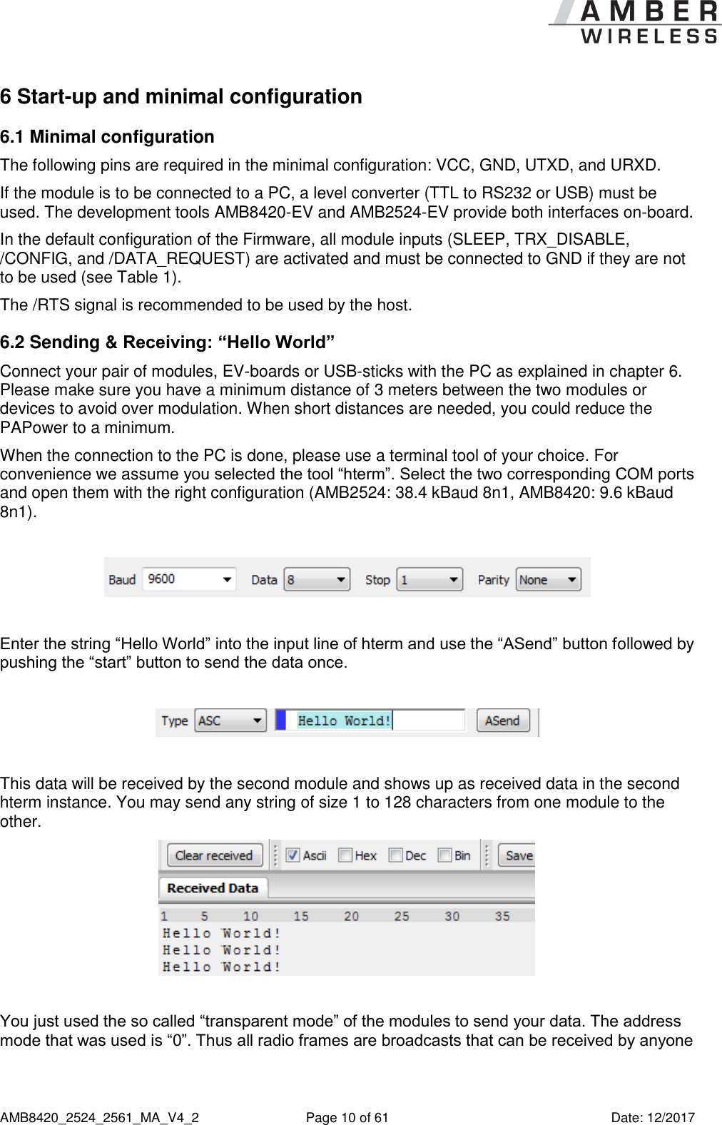
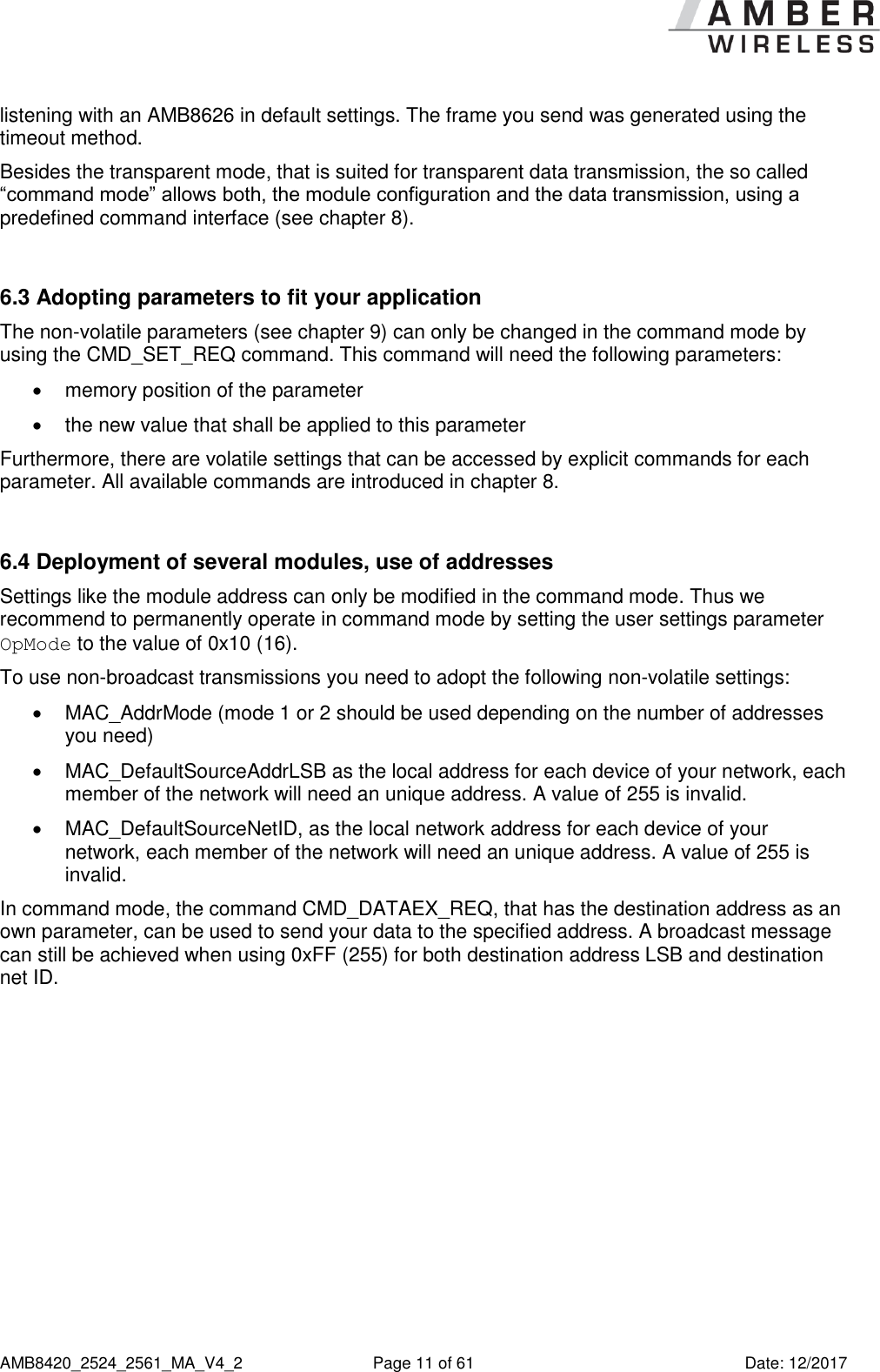
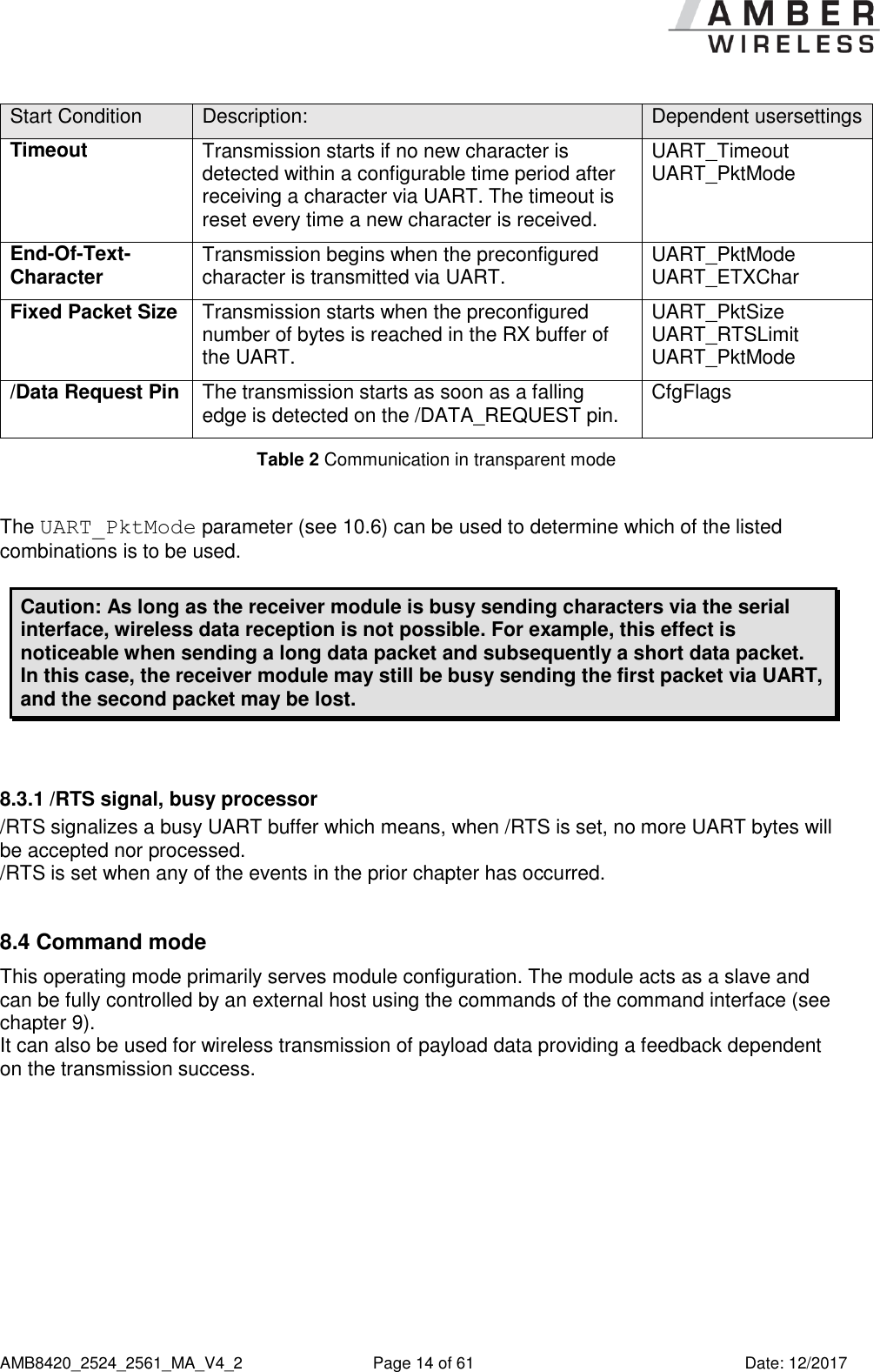
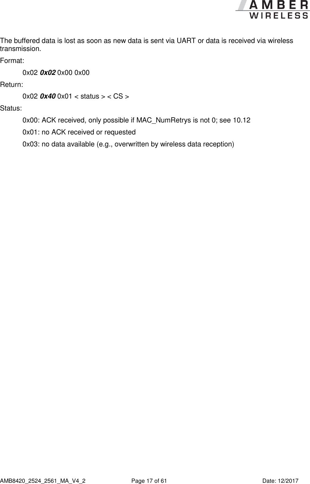
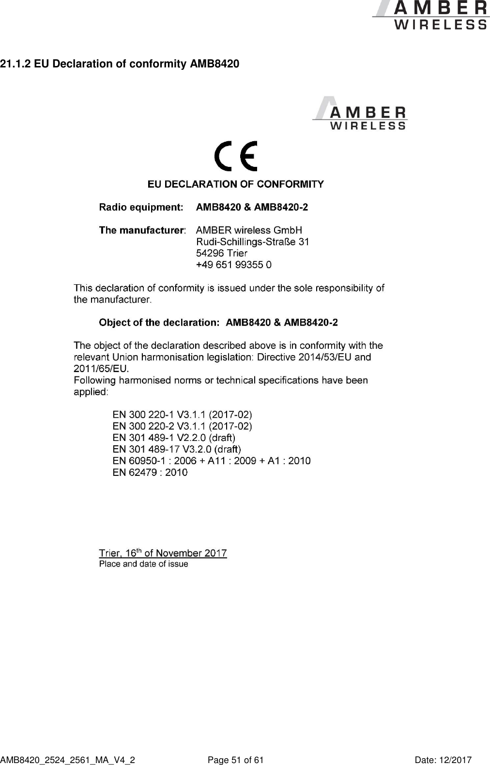
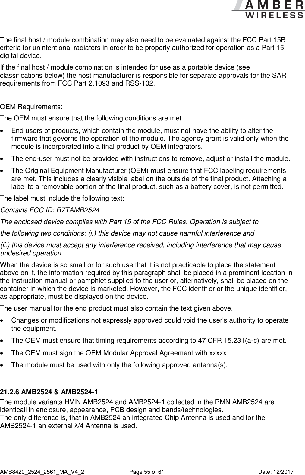
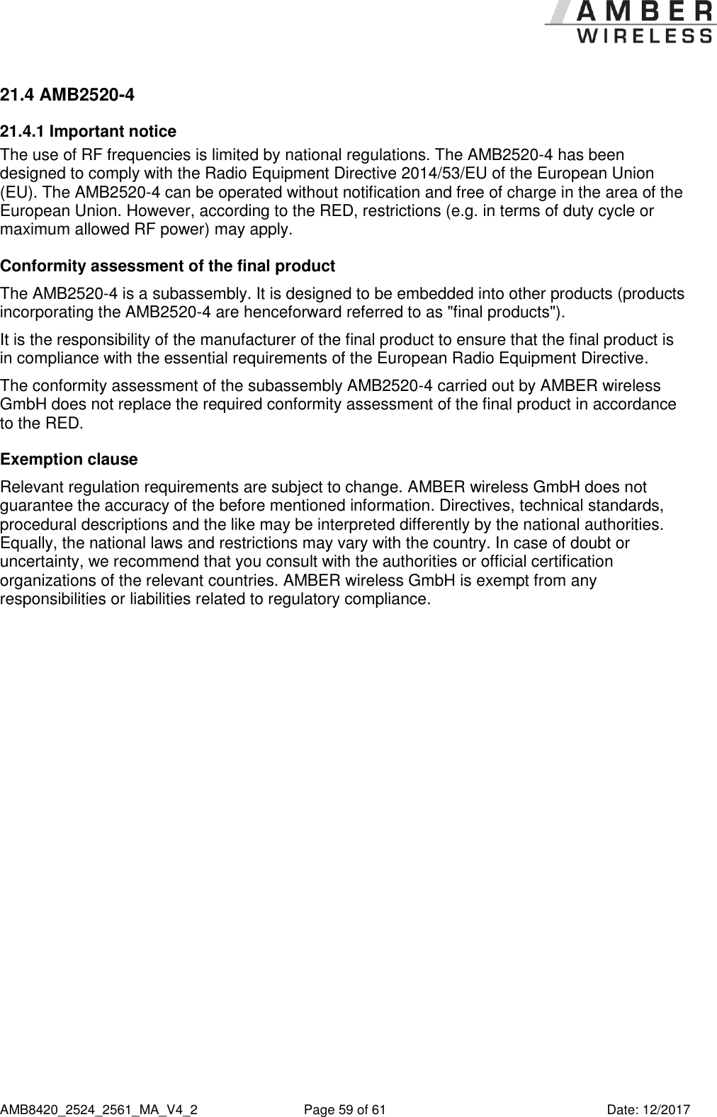
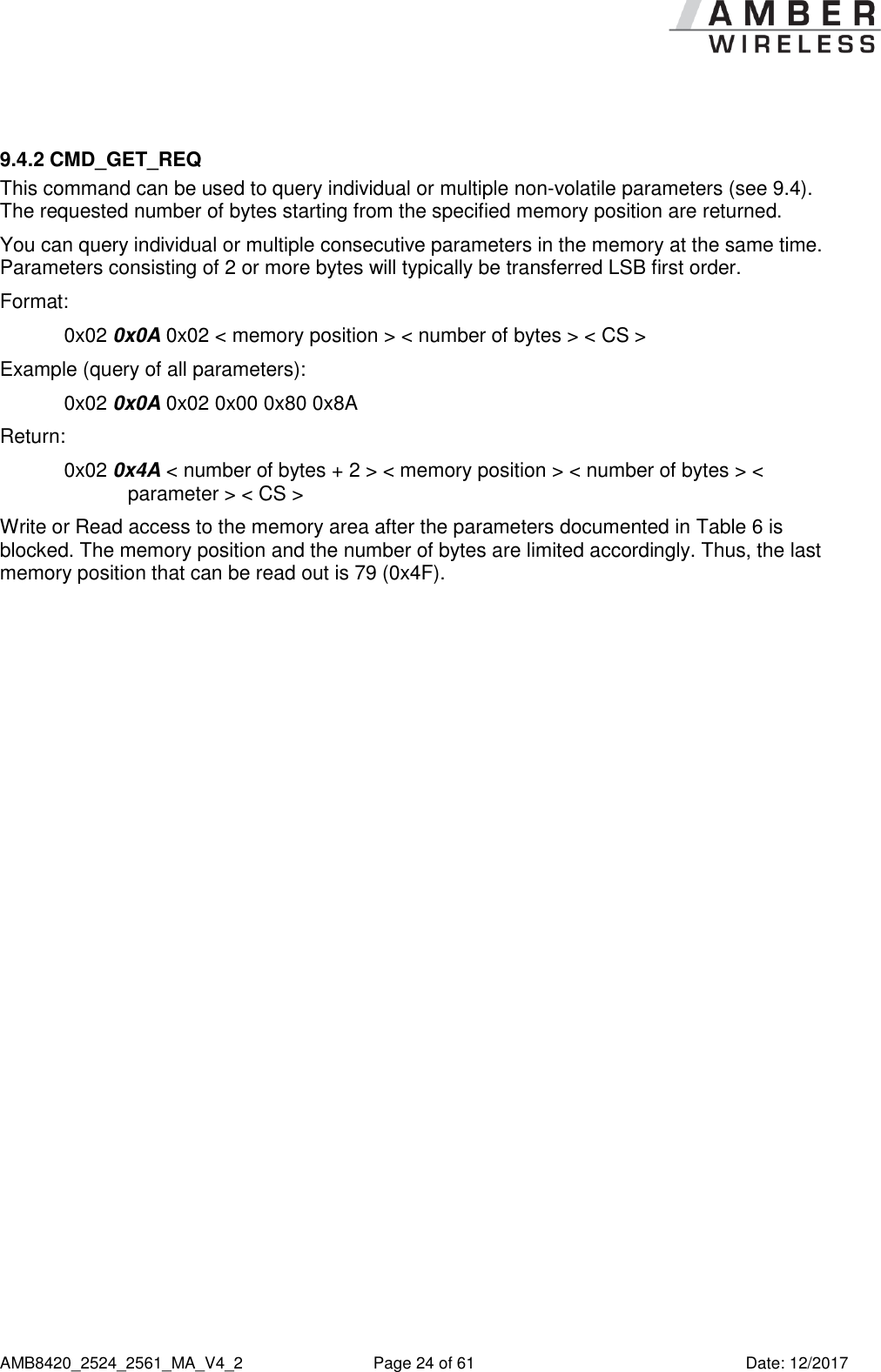
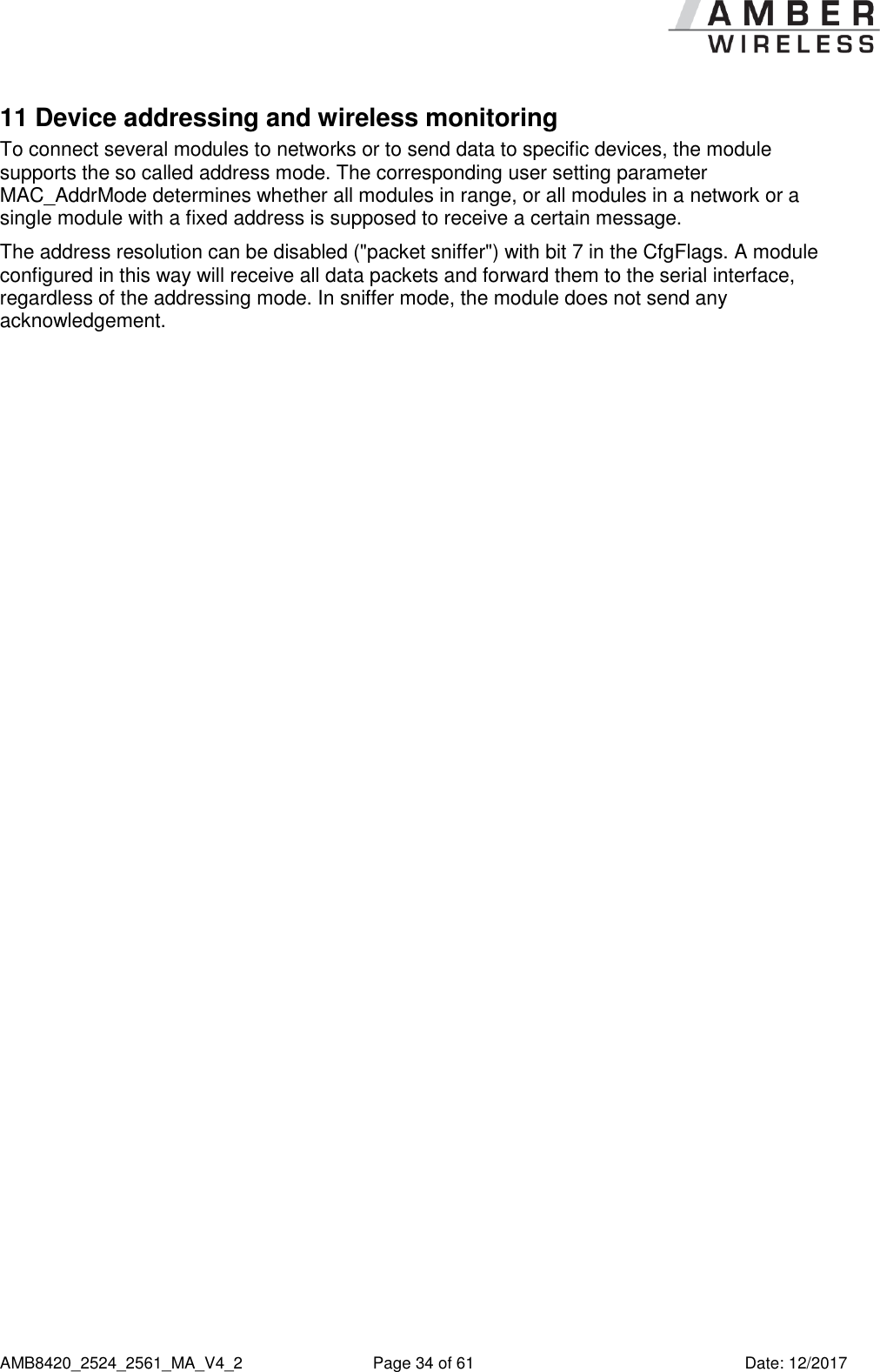
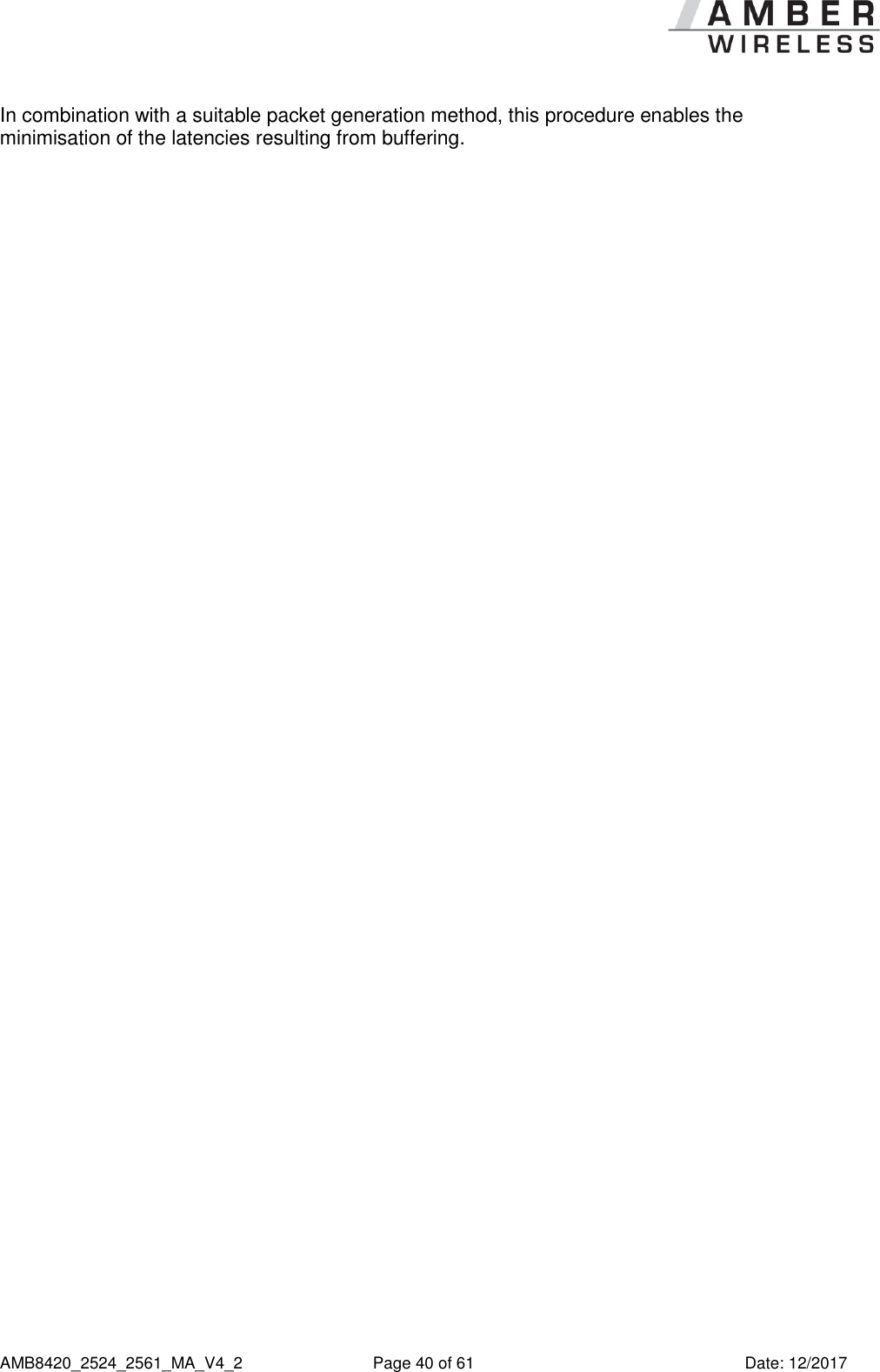
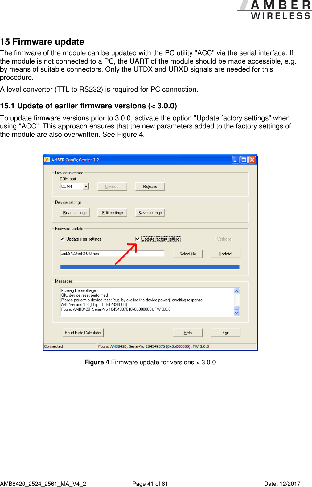
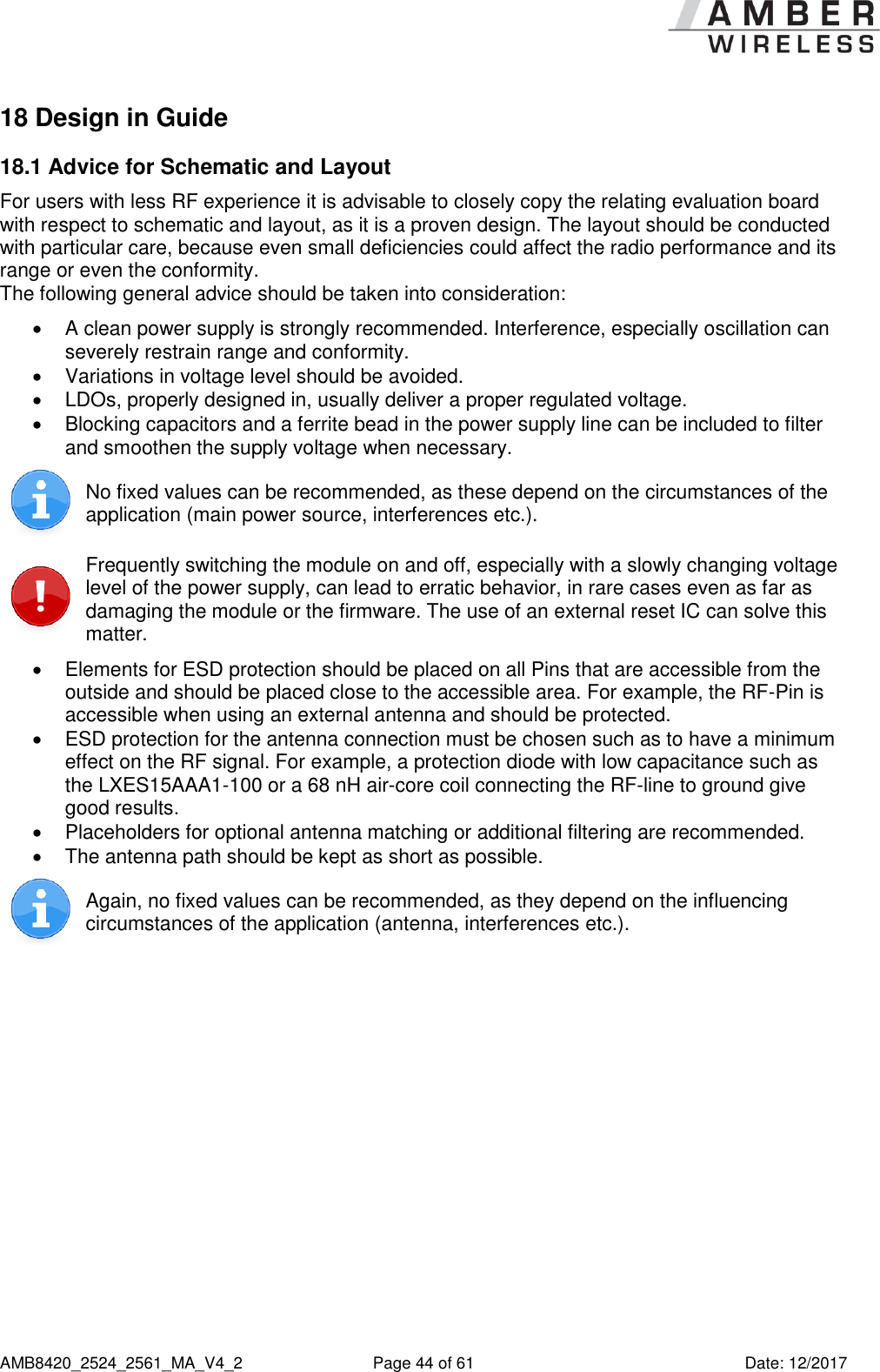
![AMB8420_2524_2561_MA_V4_2 Page 19 of 61 Date: 12/2017 3. Otherwise (RSSIdec < 128): RSSIdBm = RSSIdec / 2 - RSSIOffset RSSIOffset is a data-rate-dependent correction factor according to Table 4 (AMB8420) and Table 5 (AMB2524). The relation between the calculated value and the physical RX level in dBm is not linear across the entire operating range and is displayed in Figure 2 and Figure 3 . Data rate RSSI offset 1.2 kbps 74 38.4 kbps 74 250 kbps 78 Table 4 Data rate-dependent RSSI offset for AMB8420 (from [2]) Data rate RSSI offset 2.4 kbps 71 10 kbps 69 250 kbps 72 500 kbps 72 Table 5 Data rate-dependent RSSI offset for AMB2524 (from [3]) Figure 2 Relation between the RX level and the RSSI value read out for AMB8420 (from [2])](https://usermanual.wiki/Wuerth-Elektronik-eiSos-and-Co-KG/AMB2524/User-Guide-3737675-Page-20.png)
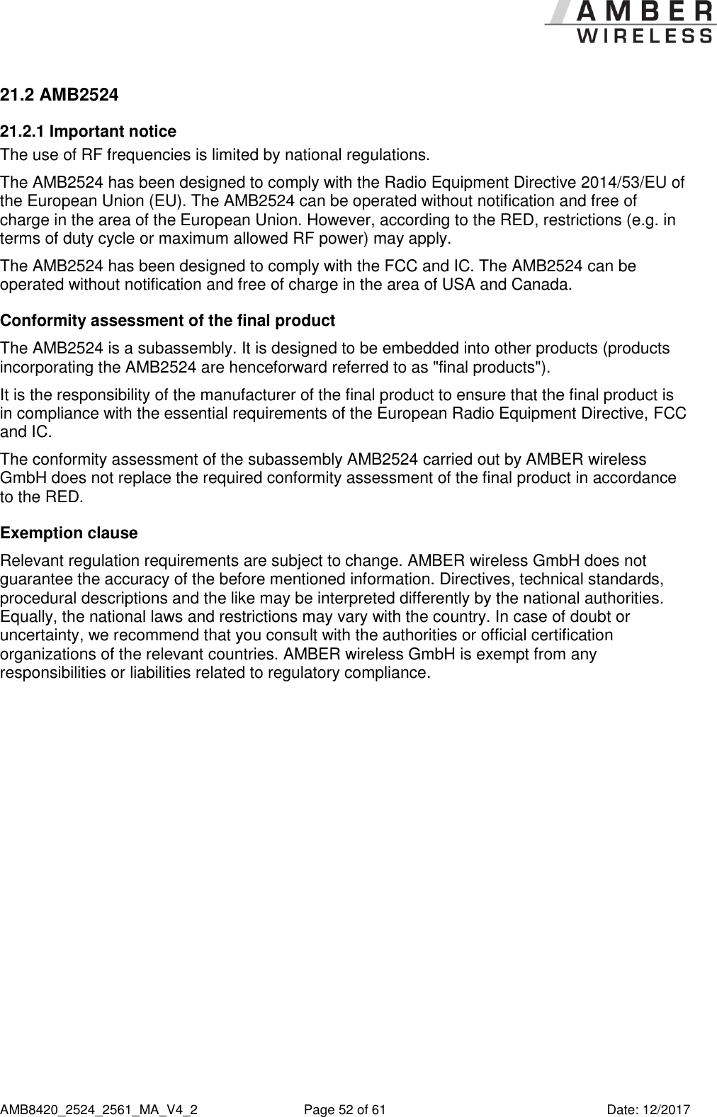
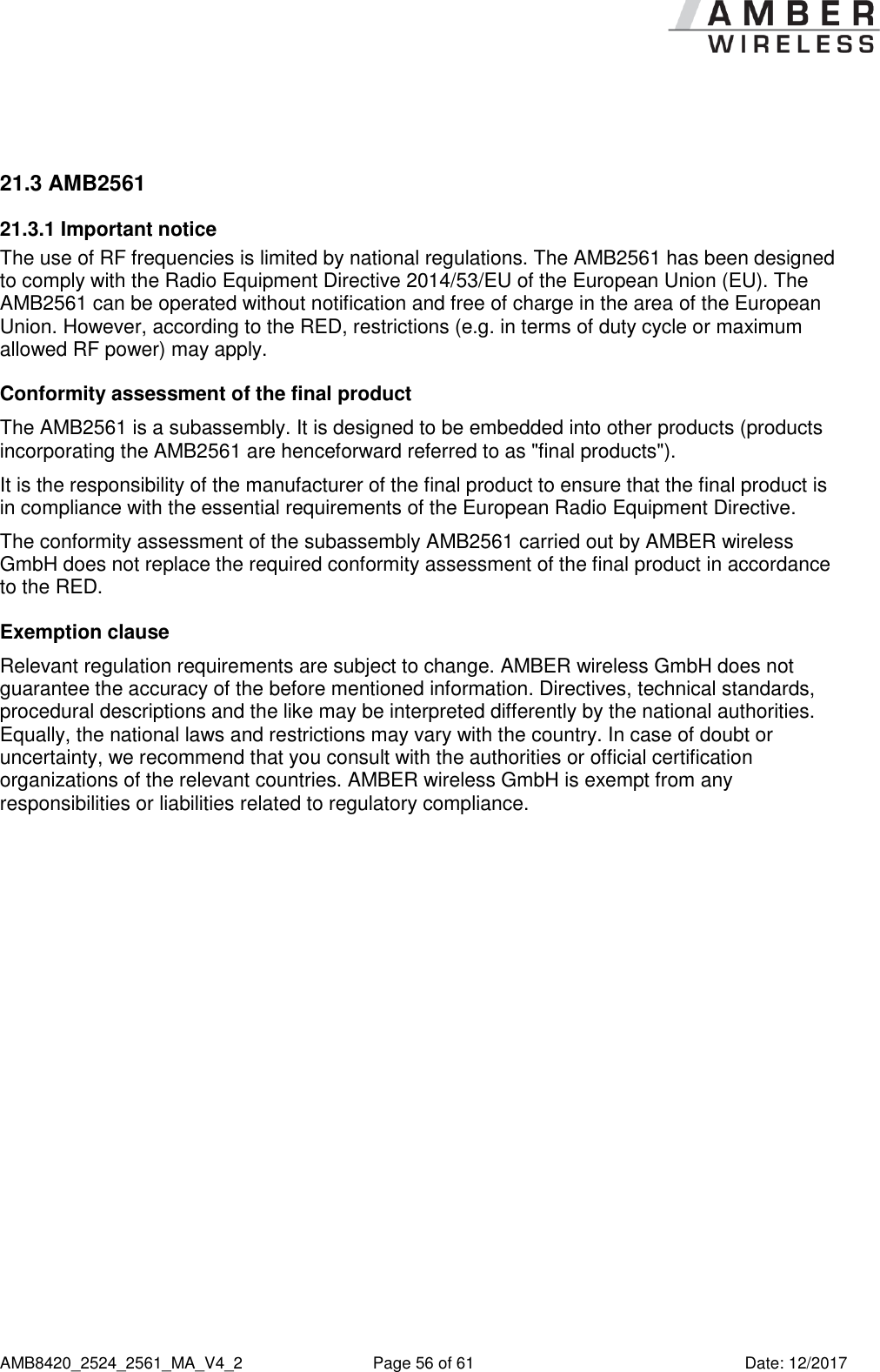
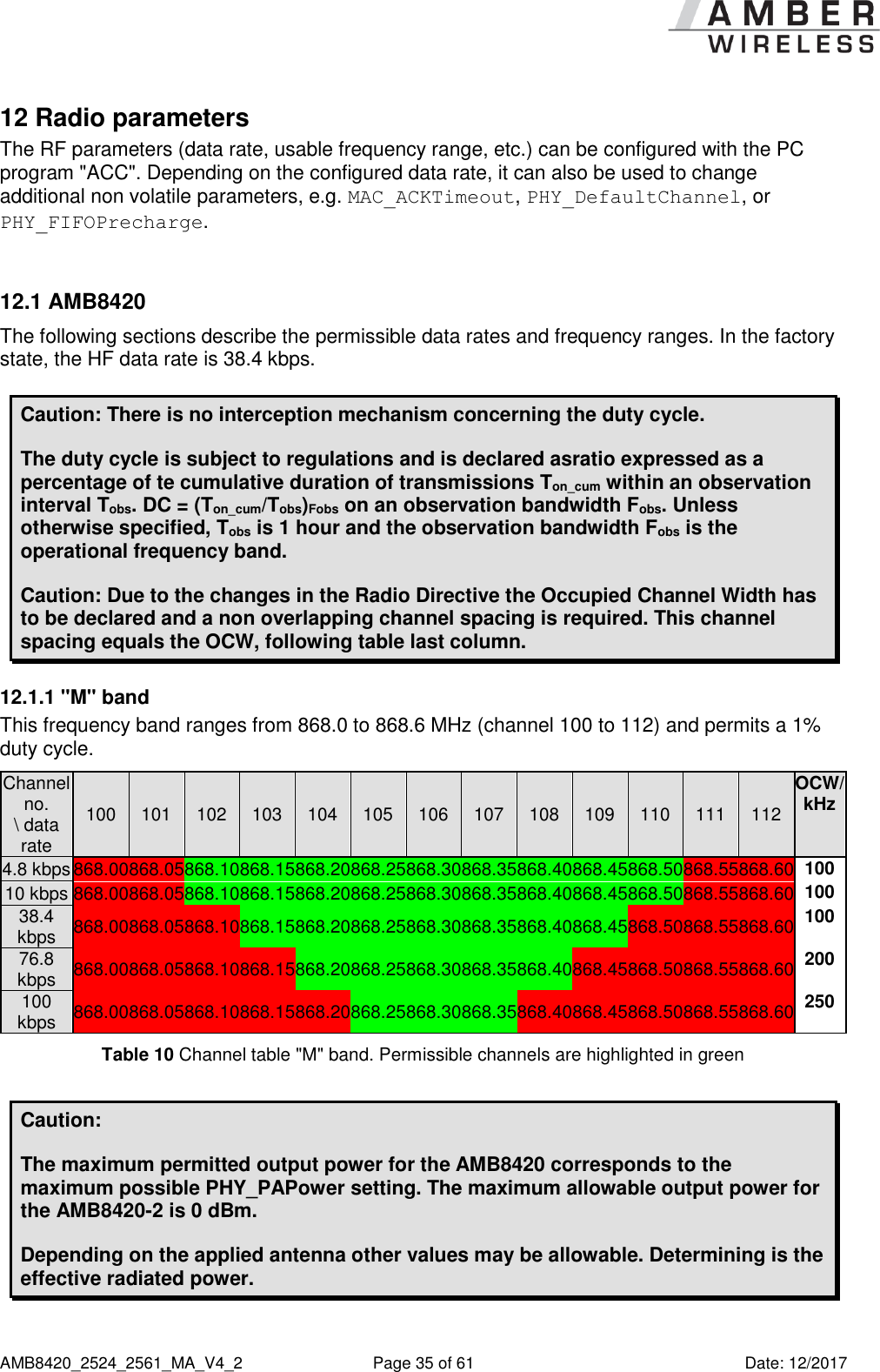
![AMB8420_2524_2561_MA_V4_2 Page 20 of 61 Date: 12/2017 Figure 3 Relation between the RX level and the RSSI value read out for AMB2524 (from [3]) 9.2.4 CMD_ERRORFLAGS_REQ This command returns internal error states. Format: 0x02 0x0E 0x00 0x0C Return: 0x02 0x4E 0x02 < error flags MSB > < error flags LSB >< CS > An error flag return value of "0" indicates that no error has occurred. The value is set back after the query and in the event of a reset. The meaning of the error flags is not described in detail in this context.](https://usermanual.wiki/Wuerth-Elektronik-eiSos-and-Co-KG/AMB2524/User-Guide-3737675-Page-21.png)
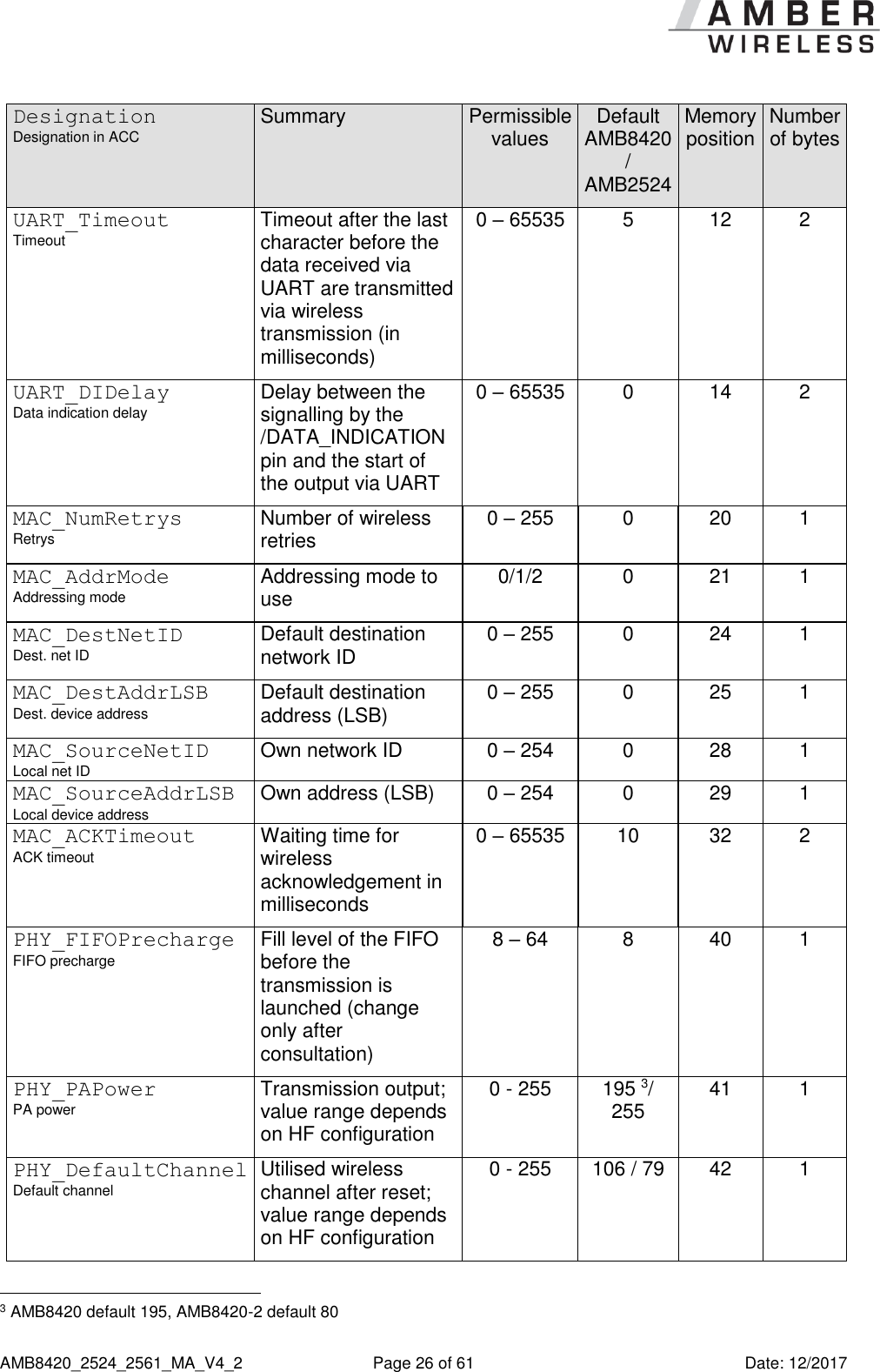
![AMB8420_2524_2561_MA_V4_2 Page 25 of 61 Date: 12/2017 10 User settings The non-volatile parameters listed in the following table can be modified by means of specific commands in the configuration mode (CMD_SET_REQ, see 9.4) of the module or by using the Windows software "ACC". These parameters are stored permanently in the module's flash memory. Caution: The validity of the specified parameters is not verified. Incorrect values can result in device malfunction! Designation Designation in ACC Summary Permissible values Default AMB8420 / AMB2524 Memory position Number of bytes UART_CTL Data format Control register for UART data format See description 16 0 1 UART_TCTL Control register for the baud rate (change only after consultation) 32 32 1 1 UART_MCTL MCTL Control register for fine-adjusting the UART baud rate; concerning the calculation, see [1] 0 - 255 0 / 68 2 1 UART_BR0 BR0 Prescaler for setting the baud rate (LSB); concerning the calculation, see [1] 0 - 255 113 / 156 3 1 UART_BR1 BR1 Prescaler for setting the baud rate (MSB); concerning the calculation, see [1] 0 - 255 2 / 0 4 1 UART_PktMode Packetizing mode Selects the packet generation method 0 or 1 0 5 1 UART_PktSize Packet size Number of characters for transmission start with set packet size 1 - 128 128 7 1 UART_RTSLimit /RTS limit Number of received characters after which /RTS responds 1 - 128 112 8 1 UART_ETXChar ETX character End-of-text character used to mark data packets; reception of this character triggers wireless transmission 0 - 255 10 9 1](https://usermanual.wiki/Wuerth-Elektronik-eiSos-and-Co-KG/AMB2524/User-Guide-3737675-Page-26.png)
![AMB8420_2524_2561_MA_V4_2 Page 28 of 61 Date: 12/2017 10.1 UART_CTL The UART data format can be configured with the help of the upper 4 bits in this register. The meaning of these bits is described in Table 7. Bit no. Description 0 to 3 (0x0F) Reserved, must always be set to 0. 4 (0x10) If this bit is set, the character length will be 8 bits, if not, it will be 7 bits. 5 (0x20) This bit selects the number of stop bits. If this bit is set, 2 stop bits will be used, if not, 1 will be used. 6 (0x40) If this bit is set, even parity will be used, if not, odd parity will be used. This bit is only used if bit 7 is set to ‘1’. 7 (0x80) This bit enables the use of parity (if set). Table 7 Setting the data format 10.2 UART_TCTL This register selects the source for generating the UART clock speed. Currently, the only permissible value is 32. 10.3 UART_MCTL The registers UART_MCTL, UART_BR0, and UART_BR1 can be used to set the UART baud rate. Concerning the calculation of the corresponding settings, see [1]. 10.4 UART_BR0 The registers UART_MCTL, UART_BR0, and UART_BR1 can be used to set the UART baud rate. Concerning the calculation of the corresponding settings, see [1]. 10.5 UART_BR1 The registers UART_MCTL, UART_BR0, and UART_BR1 can be used to set the UART baud rate. Concerning the calculation of the corresponding settings, see [1] 10.6 UART_PktMode Selects the method used for generating packets for the transparent operating mode. Two methods have been implemented: 0. Mode 0: Sends when](https://usermanual.wiki/Wuerth-Elektronik-eiSos-and-Co-KG/AMB2524/User-Guide-3737675-Page-29.png)
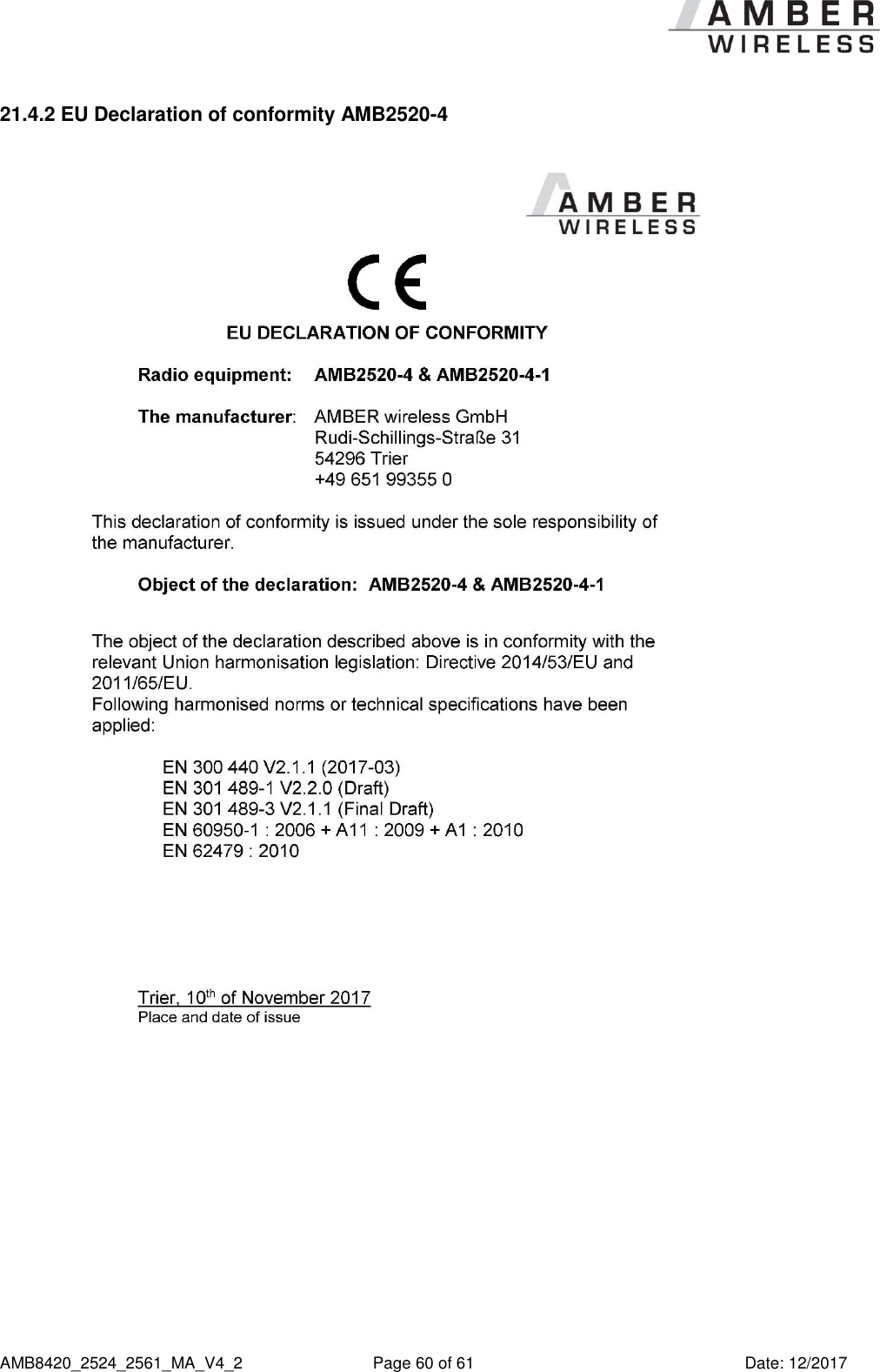
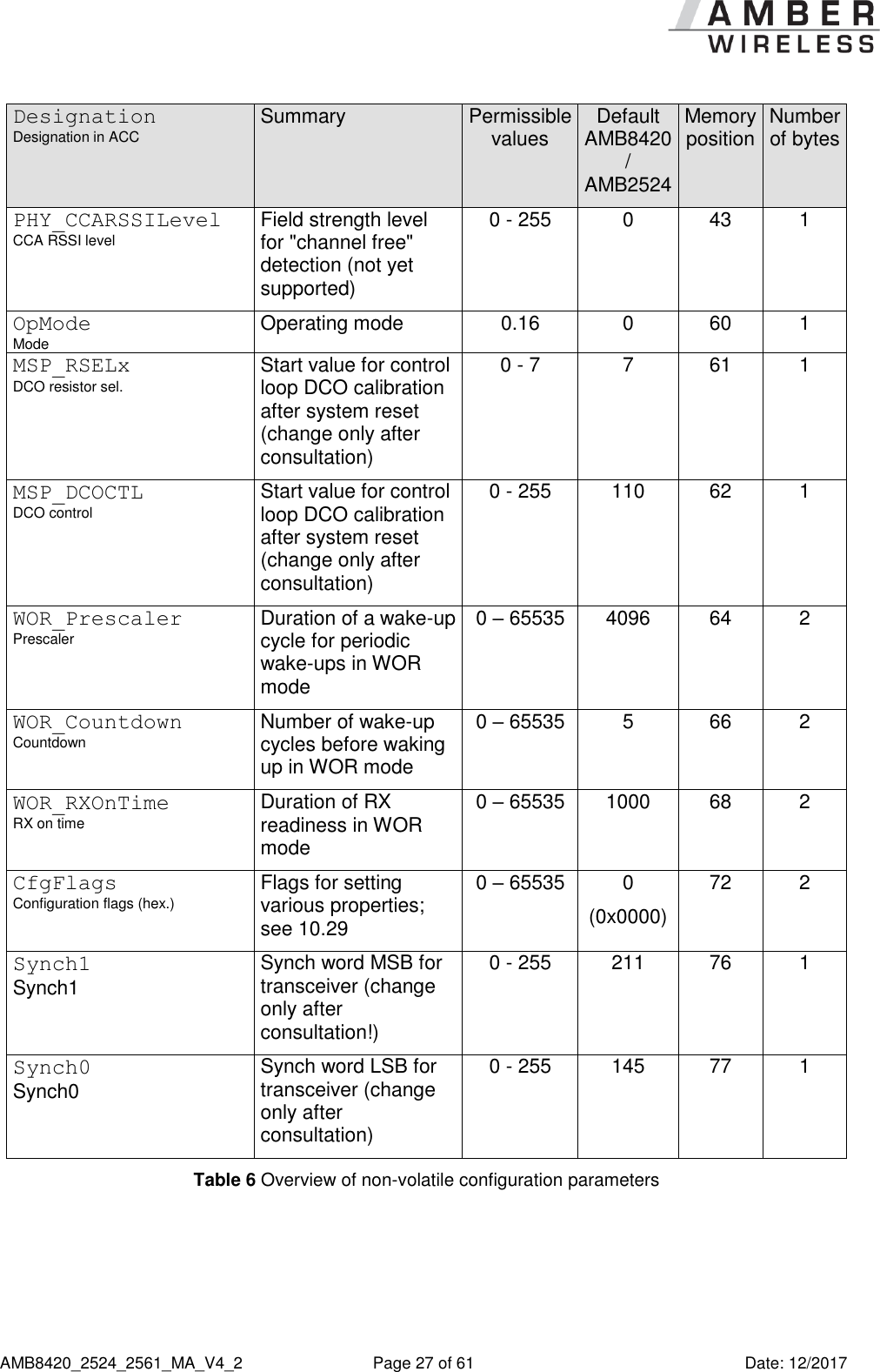
![AMB8420_2524_2561_MA_V4_2 Page 36 of 61 Date: 12/2017 12.2 AMB2524 In the factory state, the HF data rate is 250 kbps. The module AMB2524 uses a channel spacing of approximately 500 kHz; the carrier frequency can be determined with the following formula: )500.0(5.2400][ ChannelC NMHzF Here, the channels 0 to 165 are permissible. See Table 11 for an overview of usable frequencies. Caution: Avoid the channels/frequencies (2405 MHz + n x 13MHz) marked in red, which merely provide a reduced range due to a property of the wireless IC. Channel no. Freq. [MHz] Channel no. Freq. [MHz] Channel no. Freq. [MHz] Channel no. Freq. [MHz] 0 2400.5 41 2421.0 82 2441.5 123 2462.0 1 2401.0 42 2421.5 83 2442.0 124 2462.5 2 2401.5 43 2422.0 84 2442.5 125 2463.0 3 2402.0 44 2422.5 85 2443.0 126 2463.5 4 2402.5 45 2423.0 86 2443.5 127 2464.0 5 2403.0 46 2423.5 87 2444.0 128 2464.5 6 2403.5 47 2424.0 88 2444.5 129 2465.0 7 2404.0 48 2424.5 89 2445.0 130 2465.5 8 2404.5 49 2425.0 90 2445.5 131 2466.0 9 2405.0 50 2425.5 91 2446.0 132 2466.5 10 2405.5 51 2426.0 92 2446.5 133 2467.0 11 2406.0 52 2426.5 93 2447.0 134 2467.5 12 2406.5 53 2427.0 94 2447.5 135 2468.0 13 2407.0 54 2427.5 95 2448.0 136 2468.5 14 2407.5 55 2428.0 96 2448.5 137 2469.0 15 2408.0 56 2428.5 97 2449.0 138 2469.5 16 2408.5 57 2429.0 98 2449.5 139 2470.0 17 2409.0 58 2429.5 99 2450.0 140 2470.5 18 2409.5 59 2430.0 100 2450.5 141 2471.0 19 2410.0 60 2430.5 101 2451.0 142 2471.5 20 2410.5 61 2431.0 102 2451.5 143 2472.0 21 2411.0 62 2431.5 103 2452.0 144 2472.5 22 2411.5 63 2432.0 104 2452.5 145 2473.0 23 2412.0 64 2432.5 105 2453.0 146 2473.5 24 2412.5 65 2433.0 106 2453.5 147 2474.0 25 2413.0 66 2433.5 107 2454.0 148 2474.5 26 2413.5 67 2434.0 108 2454.5 149 2475.0 27 2414.0 68 2434.5 109 2455.0 150 2475.5 28 2414.5 69 2435.0 110 2455.5 151 2476.0 29 2415.0 70 2435.5 111 2456.0 152 2476.5 30 2415.5 71 2436.0 112 2456.5 153 2477.0 31 2416.0 72 2436.5 113 2457.0 154 2477.5 32 2416.5 73 2437.0 114 2457.5 155 2478.0](https://usermanual.wiki/Wuerth-Elektronik-eiSos-and-Co-KG/AMB2524/User-Guide-3737675-Page-37.png)
![AMB8420_2524_2561_MA_V4_2 Page 37 of 61 Date: 12/2017 Channel no. Freq. [MHz] Channel no. Freq. [MHz] Channel no. Freq. [MHz] Channel no. Freq. [MHz] 33 2417.0 74 2437.5 115 2458.0 156 2478.5 34 2417.5 75 2438.0 116 2458.5 157 2479.0 35 2418.0 76 2438.5 117 2459.0 158 2479.5 36 2418.5 77 2439.0 118 2459.5 159 2480.0 37 2419.0 78 2439.5 119 2460.0 160 2480.5 38 2419.5 79 2440.0 120 2460.5 161 2481.0 39 2420.0 80 2440.5 121 2461.0 162 2481.5 40 2420.5 81 2441.0 122 2461.5 163 2482.0 164 2482.5 165 2483.0 Table 11 Frequency assignment AMB2524](https://usermanual.wiki/Wuerth-Elektronik-eiSos-and-Co-KG/AMB2524/User-Guide-3737675-Page-38.png)
![AMB8420_2524_2561_MA_V4_2 Page 49 of 61 Date: 12/2017 20 References [1] To calculate the baud rate registers UART_MCTL, UART_BR0, and UART_BR1, the "Baud Rate Calculator" tool is integrated in ACC. To configure a standard baud rate, ACC provides a drop-down field with automatic calculation and parameterisation of the baud rate registers. [2] "CC1101 Single-Chip Low-Cost Low-Power RF Transceiver (Rev. B)", Texas Instruments [3] "CC2500 Single-Chip Low-Cost Low-Power RF Transceiver (Rev. B)", Texas Instruments [4] "AMB8420 Data Sheet", AMBER wireless GmbH [5] "AMB2524 Data Sheet", AMBER wireless GmbH](https://usermanual.wiki/Wuerth-Elektronik-eiSos-and-Co-KG/AMB2524/User-Guide-3737675-Page-50.png)