Wuerth Elektronik eiSos and Co KG AMB2524 AMB2524 User Manual Testreport ETS 300 335
AMBER Wireless GmbH AMB2524 Testreport ETS 300 335
Users Manual

Test report no. 17011091 Page 1 of 1
EUT: AMB2524
AMB2524-1
FCC ID: R7TAMB2524
FCC Title 47 CFR Part 15
Date of issue: 2017-12-06
Date: 2017-09-07
Created: P9 Controlled: P4 Released: P1
Vers. no. 1.17
m. dudde hochfrequenz-technik
GmbH & Co. KG
Rottland 5a
51429 Bergisch Gladbach/ Germany
Tel: +49 2207-96890
Fax +49 2207-968920
Annex acc. to FCC Title 47 CFR Part 15
relating to
AMBER wireless GmbH
AMB2524
AMB2524-1
Annex no. 5
User Manual
Functional Description
Title 47 - Telecommunication
Part 15 - Radio Frequency Devices
Subpart C – Intentional Radiators
ANSI C63.4-2014
ANSI C63.10-2013


AMB8420_2524_2561_MA_V4_2 Page 2 of 61 Date: 12/2017
Table of Contents
1 Summary ................................................................................................................................ 6
2 Ordering Information ............................................................................................................. 6
3 Electrical parameters ............................................................................................................ 7
3.1 Input voltage ..................................................................................................................... 7
3.2 Power consumption .......................................................................................................... 7
3.2.1 AMB8420 ................................................................................................................... 7
3.2.2 AMB2524 ................................................................................................................... 7
4 Dimensions and weight ........................................................................................................ 7
5 Pinout ..................................................................................................................................... 8
6 Start-up and minimal configuration ................................................................................... 10
6.1 Minimal configuration ...................................................................................................... 10
6.2 Sending & Receiving: “Hello World” ................................................................................ 10
6.3 Adopting parameters to fit your application ..................................................................... 11
6.4 Deployment of several modules, use of addresses ......................................................... 11
7 Host connection: Serial interface ....................................................................................... 12
7.1 UART .............................................................................................................................. 12
7.1.1 Supported data rates ................................................................................................ 12
7.1.2 Supported data formats ............................................................................................ 12
8 Operating modes ................................................................................................................. 13
8.1 Switching from transparent to command mode ............................................................... 13
8.2 Switching from command to transparent mode ............................................................... 13
8.3 Transparent, buffered data transfer ................................................................................. 13
8.3.1 /RTS signal, busy processor ..................................................................................... 14
8.4 Command mode ............................................................................................................. 14
9 The command interface ...................................................................................................... 15
9.1 Data transfer & reception in the command mode ............................................................ 15
9.1.1 CMD_DATA_REQ .................................................................................................... 15
9.1.2 CMD_DATAEX_REQ ............................................................................................... 16
9.1.3 CMD_DATAEX_IND ................................................................................................. 16
9.1.4 CMD_DATARETRY_REQ ........................................................................................ 16
9.2 Requesting parameters and actions ................................................................................ 18
9.2.1 CMD_SERIALNO_REQ ........................................................................................... 18
9.2.2 CMD_RESET_REQ .................................................................................................. 18
9.2.3 CMD_RSSI_REQ ..................................................................................................... 18
9.2.4 CMD_ERRORFLAGS_REQ ..................................................................................... 20
9.3 Modification of volatile parameters .................................................................................. 21
9.3.1 CMD_SET_MODE_REQ .......................................................................................... 21
9.3.2 CMD_SET_CHANNEL_REQ .................................................................................... 21
9.3.3 CMD_SET_DESTNETID_REQ................................................................................. 21
9.3.4 CMD_SET_DESTADDR_REQ ................................................................................. 22
9.4 Modification of non-volatile parameters ........................................................................... 23
9.4.1 CMD_SET_REQ ...................................................................................................... 23
9.4.2 CMD_GET_REQ ...................................................................................................... 24
10 User settings ...................................................................................................................... 25
10.1 UART_CTL ................................................................................................................... 28
10.2 UART_TCTL ................................................................................................................. 28
10.3 UART_MCTL ................................................................................................................ 28
10.4 UART_BR0 ................................................................................................................... 28

AMB8420_2524_2561_MA_V4_2 Page 3 of 61 Date: 12/2017
10.5 UART_BR1 ................................................................................................................... 28
10.6 UART_PktMode ............................................................................................................ 28
10.7 UART_PktSize .............................................................................................................. 29
10.8 UART_RTSLimit ........................................................................................................... 29
10.9 UART_ETXChar ........................................................................................................... 29
10.10 UART_Timeout ........................................................................................................... 29
10.11 UART_DIDelay ........................................................................................................... 29
10.12 MAC_NumRetrys ........................................................................................................ 30
10.13 MAC_AddrMode ......................................................................................................... 30
10.14 MAC_DestNetID ......................................................................................................... 30
10.15 MAC_DestAddrLSB .................................................................................................... 30
10.16 MAC_SourceNetID ..................................................................................................... 31
10.17 MAC_SourceAddrLSB ................................................................................................ 31
10.18 MAC_ACKTimeout ...................................................................................................... 31
10.19 PHY_FIFOPrecharge .................................................................................................. 31
10.20 PHY_PAPower ............................................................................................................ 31
10.21 PHY_DefaultChannel .................................................................................................. 31
10.22 PHY_CCARSSILevel .................................................................................................. 32
10.23 OpMode ...................................................................................................................... 32
10.24 MSP_RSELx ............................................................................................................... 32
10.25 MSP_DCOCTL ........................................................................................................... 32
10.26 WOR_Prescaler .......................................................................................................... 32
10.27 WOR_Countdown ....................................................................................................... 32
10.28 WOR_RXOnTime ....................................................................................................... 32
10.29 CfgFlags ..................................................................................................................... 32
11 Device addressing and wireless monitoring ................................................................... 34
12 Radio parameters .............................................................................................................. 35
12.1 AMB8420 ...................................................................................................................... 35
12.1.1 "M" band ................................................................................................................. 35
12.2 AMB2524 ...................................................................................................................... 36
13 Battery powered operation ............................................................................................... 38
13.1 Active mode .................................................................................................................. 38
13.2 Stand-by ....................................................................................................................... 38
13.3 WOR mode ................................................................................................................... 38
13.4 Sleep mode ................................................................................................................... 38
14 Timing parameters ............................................................................................................ 39
14.1 Reset behaviour ............................................................................................................ 39
14.1.1 Power-on reset ....................................................................................................... 39
14.1.2 Reset via /RESET pin ............................................................................................. 39
14.2 Wake-up from the sleep mode ...................................................................................... 39
14.3 Latencies during data transfer / packet generation ........................................................ 39
15 Firmware update ................................................................................................................ 41
15.1 Update of earlier firmware versions (< 3.0.0) ................................................................. 41
16 Firmware history ............................................................................................................... 42
17 Manufacturing information ............................................................................................... 43
17.1 Footprint dimensioning proposal ................................................................................... 43
18 Design in Guide ................................................................................................................. 44
18.1 Advice for Schematic and Layout .................................................................................. 44
18.2 Dimensioning of the 50 Ohm microstrip ........................................................................ 46

AMB8420_2524_2561_MA_V4_2 Page 4 of 61 Date: 12/2017
18.3 Antenna solutions ......................................................................................................... 47
18.3.1 Lambda/4 radiator .................................................................................................. 47
18.3.2 Chip antenna .......................................................................................................... 47
18.3.3 PCB antenna .......................................................................................................... 47
19 Manufacturing information ............................................................................................... 48
20 References ......................................................................................................................... 49
21 Regulatory compliance information ................................................................................. 50
21.1 AMB8420 ...................................................................................................................... 50
21.1.1 Important notice ...................................................................................................... 50
21.1.2 EU Declaration of conformity AMB8420 .................................................................. 51
21.2 AMB2524 ...................................................................................................................... 52
21.2.1 Important notice ...................................................................................................... 52
21.2.2 EU Declaration of conformity AMB2524 .................................................................. 53
21.2.3 FCC Compliance statement AMB2524 & AMB2524-1 ............................................ 54
21.2.4 IC Compliance statement AMB2524 & AMB2524-1 ................................................ 54
21.2.5 FCC and IC Requirements to OEM integrators ....................................................... 54
21.2.6 AMB2524 & AMB2524-1 ......................................................................................... 55
21.3 AMB2561 ...................................................................................................................... 56
21.3.1 Important notice ...................................................................................................... 56
21.3.2 EU Declaration of conformity AMB2561 .................................................................. 57
21.3.3 FCC statement ....................................................................................................... 58
21.4 AMB2520-4 ................................................................................................................... 59
21.4.1 Important notice ...................................................................................................... 59
21.4.2 EU Declaration of conformity AMB2520-4 .............................................................. 60
22 Important information ....................................................................................................... 61
22.1 Exclusion of liability ....................................................................................................... 61
22.2 Trademarks ................................................................................................................... 61
22.3 Usage restriction ........................................................................................................... 61

AMB8420_2524_2561_MA_V4_2 Page 5 of 61 Date: 12/2017
Abbreviations
CS
Checksum
DC
Duty cycle
Relative frequency reservation period

AMB8420_2524_2561_MA_V4_2 Page 6 of 61 Date: 12/2017
1 Summary
The AMB8420/AMB2524 module was designed as a radio submodule for wireless
communication between devices like controls, remote controls, sensors etc. It offers several
addressing modes and relieves the host system of radio-specific tasks such as
checksum calculation,
address resolution and
repetition of unacknowledged telegrams.
It can be deployed wherever the wireless exchange of small data packets (up to 128 bytes)
between two or more parties is required.
A serial interface (UART) whose data rate and format can be adjusted flexibly is available for
communicating with the host system.
By means of the Windows program "ACC", the HF data rate can be adjusted from 4.8 to 250
kbps.
Thanks to its small size and the integrated antenna, the module can easily be installed in
existing systems without any external circuits.
2 Ordering Information
Item no.
Description
AMB2524
2.4 GHz RF module with integrated ceramic antenna
AMB2524-TR
AMB2524 on Tape & Reel, Reflow solderable, packing unit 400pcs
AMB2524-1
2.4 GHz RF module with RF pin
AMB2524-1-TR
AMB2524-1 on Tape & Reel, Reflow solderable, packing unit 400pcs
AMB2524-2
2.4 GHz RF module with U.Fl socket
AMB2524-2-TR
AMB2524-2 on Tape & Reel, Reflow solderable, packing unit 400pcs
AMB8420
868 MHz RF module with integrated ceramic-antenna
AMB8420-TR
AMB8420 on Tape & Reel, Reflow solderable, packing unit 400pcs
AMB8420-2
868 MHz RF module with RF pin
AMB8420-2-TR
AMB8420-2 on Tape & Reel, Reflow solderable, packing unit 400pcs

AMB8420_2524_2561_MA_V4_2 Page 7 of 61 Date: 12/2017
3 Electrical parameters
3.1 Input voltage
The input voltage of the module ranges from 2.7 to 3.6 V.
In order to ensure a constant processor frequency (and UART clock rate) over the entire voltage
range, the clock rate is continuously readjusted on the basis of the available watch crystal.
Voltage changes during the reception or output over the serial interface can result in a change
of the clock rate between two characters.
Caution: A clean supply voltage is needed for the module to function correctly.
Using a 100 µF blocking capacitor close to the VCC pin is a useful measure
(especially when using RS232 converters or clocked DC-DC converters).
3.2 Power consumption
3.2.1 AMB8420
See data sheet [4].
3.2.2 AMB2524
See data sheet [5].
Caution: To minimize power consumption in Sleep Mode, the input signals of the
module (/CONFIG, SLEEP, TRX_DISABLE und /DATA_REQUEST) must be set to the
levels defined in Table 1. Open (floating) pins result in increased power
consumption.
4 Dimensions and weight
See data sheets [4] and [5].
AMB8420_2524_2561_MA_V4_2 Page 8 of 61 Date: 12/2017
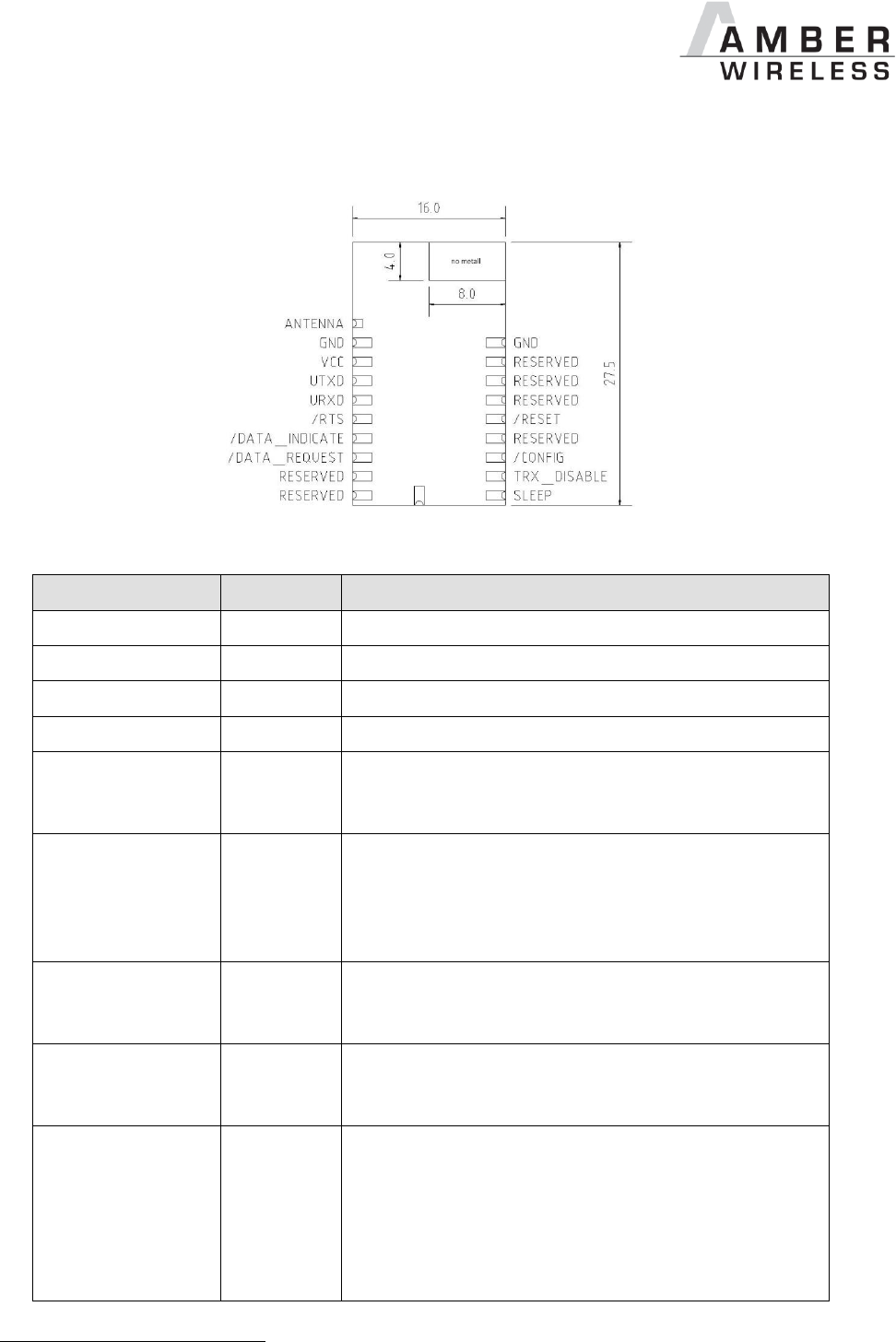
5 Pinout
Figure 1 Pinout
Designation
I/O
Description
VCC1
Supply
Supply voltage
GND
Supply
Ground
UTXD
Output
Output serial interface
URXD
Input
Input serial interface
/RESET
Input
A low level on this pin performs a restart of the
module. Internally, this pin is connected to VCC via a
100 kΩ pull-up resistor. Leave open if not needed.
/CONFIG
Input
Used to switch the module to the command mode
(falling edge). Alternatively, this can be done by
means of a UART break signal. Connect to GND if
not needed. The function can be disabled (see
10.29).
SLEEP
Input
Activates the Sleep Mode (high level). Connect to
GND if not needed. The function can be disabled
(see 10.29).
TRX_DISABLE
Input
Switches the HF part off (high level) as long as no
data is to be sent. Connect to GND if not needed.
The function can be disabled (see 10.29).
/DATA_REQUEST
Input
Prompts the wireless transmission of the data
received via the UART (falling edge). As long as no
new data is received via UART or wireless
transmission, the buffer content remains valid and
can be resent by means of a new signal. Connect to
GND if not needed. The function can be disabled
(see 10.29). Without function in the command mode.
1
100µF blocking capacitor recommended between VCC and GND in close proximity to the module

AMB8420_2524_2561_MA_V4_2 Page 9 of 61 Date: 12/2017
/RTS
Output
Ready to send (active low). When /RTS is low, data
can be received via UART. /RTS goes high as soon
as the UART buffer is full or when the wireless
reception of a telegram is detected. From this
moment, all data coming in via UART will be
ignored. Timeout after falling edge: 100 µs.
/DATA_INDICATE
Output
Goes low as soon as a valid frame is received via
wireless transmission and remains low as long as
the output via UART continues. Can be used to
prepare a "sleeping" host system for the output of
data. The delay between the falling edge and the
beginning of output via UART can be configured
(see UART_DIDelay, 10.11). During the
transmission process, this pin signals the successful
acknowledgement of the wireless telegram (if such
was requested, see MAC_NumRetrys, 10.12): in
this case, /DATA_INDICATE is set to low before the
falling edge of the /RTS pin and goes back high
when new data is received via wireless transmission
or UART, at the latest.
RESERVED
Currently not used. These pins must be left open (do
not connect). Some of these pins are used for the
optional SPI2 interface.
N.C.
Open, optional aerial connection; use only after
consultation.
Table 1 Pinout
2
An SPI interface can be implemented upon request.
AMB8420_2524_2561_MA_V4_2 Page 10 of 61 Date: 12/2017
6 Start-up and minimal configuration
6.1 Minimal configuration
The following pins are required in the minimal configuration: VCC, GND, UTXD, and URXD.
If the module is to be connected to a PC, a level converter (TTL to RS232 or USB) must be
used. The development tools AMB8420-EV and AMB2524-EV provide both interfaces on-board.
In the default configuration of the Firmware, all module inputs (SLEEP, TRX_DISABLE,
/CONFIG, and /DATA_REQUEST) are activated and must be connected to GND if they are not
to be used (see Table 1).
The /RTS signal is recommended to be used by the host.
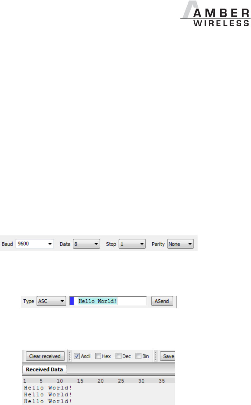
6.2 Sending & Receiving: “Hello World”
Connect your pair of modules, EV-boards or USB-sticks with the PC as explained in chapter 6.
Please make sure you have a minimum distance of 3 meters between the two modules or
devices to avoid over modulation. When short distances are needed, you could reduce the
PAPower to a minimum.
When the connection to the PC is done, please use a terminal tool of your choice. For
convenience we assume you selected the tool “hterm”. Select the two corresponding COM ports
and open them with the right configuration (AMB2524: 38.4 kBaud 8n1, AMB8420: 9.6 kBaud
8n1).
Enter the string “Hello World” into the input line of hterm and use the “ASend” button followed by
pushing the “start” button to send the data once.
This data will be received by the second module and shows up as received data in the second
hterm instance. You may send any string of size 1 to 128 characters from one module to the
other.
You just used the so called “transparent mode” of the modules to send your data. The address
mode that was used is “0”. Thus all radio frames are broadcasts that can be received by anyone

AMB8420_2524_2561_MA_V4_2 Page 11 of 61 Date: 12/2017
listening with an AMB8626 in default settings. The frame you send was generated using the
timeout method.
Besides the transparent mode, that is suited for transparent data transmission, the so called
“command mode” allows both, the module configuration and the data transmission, using a
predefined command interface (see chapter 8).
6.3 Adopting parameters to fit your application
The non-volatile parameters (see chapter 9) can only be changed in the command mode by
using the CMD_SET_REQ command. This command will need the following parameters:
memory position of the parameter
the new value that shall be applied to this parameter
Furthermore, there are volatile settings that can be accessed by explicit commands for each
parameter. All available commands are introduced in chapter 8.
6.4 Deployment of several modules, use of addresses
Settings like the module address can only be modified in the command mode. Thus we
recommend to permanently operate in command mode by setting the user settings parameter
OpMode to the value of 0x10 (16).
To use non-broadcast transmissions you need to adopt the following non-volatile settings:
MAC_AddrMode (mode 1 or 2 should be used depending on the number of addresses
you need)
MAC_DefaultSourceAddrLSB as the local address for each device of your network, each
member of the network will need an unique address. A value of 255 is invalid.
MAC_DefaultSourceNetID, as the local network address for each device of your
network, each member of the network will need an unique address. A value of 255 is
invalid.
In command mode, the command CMD_DATAEX_REQ, that has the destination address as an
own parameter, can be used to send your data to the specified address. A broadcast message
can still be achieved when using 0xFF (255) for both destination address LSB and destination
net ID.

AMB8420_2524_2561_MA_V4_2 Page 12 of 61 Date: 12/2017
7 Host connection: Serial interface
7.1 UART
7.1.1 Supported data rates
The data rate is adjusted by directly configuring the respective registers of the utilised
microprocessor (see UART_TCTL, UART_MCTL, UART_BR0, and UART_BR1; from 10.1). In
this way, the data rate can be adjusted freely from 0.5 to 115200 baud.
As the UART speed is derived from the speed of the utilised clock quartz, there may be
variations of up to 0.5%.
When using the PC program "ACC", the following data rates can be selected using the data rate
calculator. With this selection, the three registers above are automatically set to the optimum
value.
The default baud rate of the module is 9600 (AMB8420) / 38400 (AMB2524).
The output of characters on the serial interface takes place with secondary priority. For this
reason, short interruptions may occur between the output of individual characters (e.g. in the
event of an interrupt).
7.1.2 Supported data formats
All data formats offered by the processor are supported:
7 or 8 bits
No, even, or odd parity
1 or 2 stop bits
In ACC, the following data formats can be selected directly via the drop-down menu:
8n1, 8o1, 8e1, 8n2, 8o2, 8e2, 7n1, 7o1, 7e1, 7n2, 7o2, 7e2.
The data format, too, can be set by directly configuring the respective microprocessor registers
(see UART_CTL, 10.1).
The default and recommended data format is 8 data bits, no parity, 1 stop bit ("8n1").

AMB8420_2524_2561_MA_V4_2 Page 13 of 61 Date: 12/2017
8 Operating modes
The module can be used in the following operating modes:
1. Transparent mode (transparent data transmission)
2. Command mode (module configuration and data transmission using the predefined
command interface)
The operating mode after power-up can be configured by means of the OpMode parameter. By
default, the module operates in transparent mode.
Starting in the command mode, the module responds with a CMD_SET_MODE_CNF telegram.
8.1 Switching from transparent to command mode
The command mode can be entered by applying a falling edge on the /CONFIG pin or when a
break signal is detected on the UART. A break condition exists if the RX input of the module is
kept low for at least 10 more bits after an absent stop bit. Detection of both the falling edge on
the /CONFIG pin and of the break signal can be disabled using the user setting CfgFlags.
The successful switchover is acknowledged by a CMD_SET_MODE_CNF telegram.
The switchover can only occur when no data is being received by wireless transmission or
UART interface (approximately 100 µs after /RTS goes low and indicates readiness).
8.2 Switching from command to transparent mode
The transparent mode can be entered by applying a falling edge on the /CONFIG pin, by using
the command CMD_SET_MODE_REQ or on detection of another break signal on the UART.
Detection of both the falling edge on the /CONFIG pin and of the break signal can be disabled
using the user setting CfgFlags.
The successful switchover is acknowledged by a CMD_SET_MODE_CNF telegram.
The switchover can only occur when no data is being received by wireless transmission or
UART interface (approximately 100 µs after /RTS goes low and indicates readiness).
8.3 Transparent, buffered data transfer
In this mode, data is received via the serial interface and initially buffered. As soon as a specific
condition is met (see Table 2), the RF telegram is generated with a preamble, checksum, and
address information (optional).
The number of characters transmitted in the wireless telegram in addition to the actual payload
data depends on the selected addressing method and the data rate, and varies between 12 and
16 bytes (packet overhead).
If required, the RF telegram can be acknowledged by the recipient module (see 10.12). If no
acknowledgement is received, the telegram will automatically be repeated upon expiry of a
timeout (see 10.18).
The buffer size at the UART interface is 128 bytes, i.e. the maximum size of transmitted data
packets is 128 bytes (payload data only, without packet overhead).
To initiate an RF transmission, several options are available, listed in Table 2.

AMB8420_2524_2561_MA_V4_2 Page 14 of 61 Date: 12/2017
Start Condition
Description:
Dependent usersettings
Timeout
Transmission starts if no new character is
detected within a configurable time period after
receiving a character via UART. The timeout is
reset every time a new character is received.
UART_Timeout
UART_PktMode
End-Of-Text-
Character
Transmission begins when the preconfigured
character is transmitted via UART.
UART_PktMode
UART_ETXChar
Fixed Packet Size
Transmission starts when the preconfigured
number of bytes is reached in the RX buffer of
the UART.
UART_PktSize
UART_RTSLimit
UART_PktMode
/Data Request Pin
The transmission starts as soon as a falling
edge is detected on the /DATA_REQUEST pin.
CfgFlags
Table 2 Communication in transparent mode
The UART_PktMode parameter (see 10.6) can be used to determine which of the listed
combinations is to be used.
Caution: As long as the receiver module is busy sending characters via the serial
interface, wireless data reception is not possible. For example, this effect is
noticeable when sending a long data packet and subsequently a short data packet.
In this case, the receiver module may still be busy sending the first packet via UART,
and the second packet may be lost.
8.3.1 /RTS signal, busy processor
/RTS signalizes a busy UART buffer which means, when /RTS is set, no more UART bytes will
be accepted nor processed.
/RTS is set when any of the events in the prior chapter has occurred.
8.4 Command mode
This operating mode primarily serves module configuration. The module acts as a slave and
can be fully controlled by an external host using the commands of the command interface (see
chapter 9).
It can also be used for wireless transmission of payload data providing a feedback dependent
on the transmission success.

AMB8420_2524_2561_MA_V4_2 Page 15 of 61 Date: 12/2017
9 The command interface
In the command mode, communication with the module occurs in the form of predefined
commands. These commands must be sent in telegrams according to the format described in
Table 3.
Start signal
Command
No. of data
Data (var.)
Checksum
Table 3 Telegram format in the command mode
Start signal: STX = 0x02
Command: One of the predefined commands according to section 14 (1 byte)
No. of data: Specifies the number of data in the following field of variable length and is limited
to 128 in order to prevent buffer overflow (1 byte)
Data: Variable number of data or parameters (maximum 128 byte, LSB first)
Checksum: XOR relation of the preceding fields including the start signal STX, i.e. 0x02 ^
command ^ no. of data ^ data byte 0 ... (1 byte)
Using a specific command, data can also be sent via HF, i.e. the module can be operated
entirely in the command mode. This is useful for realising quick channel changes, for example.
If no new signal is received for UART_Timeout milliseconds (see 10.10) after receiving the
STX signal, the unit will wait for a new start signal.
9.1 Data transfer & reception in the command mode
This chapter describes the commands to directly control the module, particular the data
transmission over the radio link (when the module is in the command mode).
9.1.1 CMD_DATA_REQ
This command serves the simple data transfer in the command mode. Transmission takes place
on the configured channel (see 9.3.2) to the previously parameterised destination address (see
9.3.3 and 9.3.4).
This command is especially suitable for transmission on a point-to-point connection. The
number of payload data bytes is limited to 128 in order to prevent buffer overflow.
Format (limit 128 payload data bytes):
0x02 0x00 < number of payload data bytes > < payload data bytes > < CS >
Return:
0x02 0x40 0x01 < status > < CS >
Status:
0x00: ACK received, only possible if MAC_NumRetrys is not 0; see 10.12
0x01: no ACK received or requested

AMB8420_2524_2561_MA_V4_2 Page 16 of 61 Date: 12/2017
9.1.2 CMD_DATAEX_REQ
This command serves data transfer in a network with several parties. Both the channel to use
and the destination address (depending on the parameterised addressing mode) are specified
along with the command. The number of payload data bytes is limited to 127, 126, or 125 in
order to prevent buffer overflow.
Format in addressing mode 0 (limit 127 payload data bytes):
0x02 0x01 < number of payload data bytes + 1 > < channel > < payload data bytes > <
CS >
Format in addressing mode 1 (limit 126 payload data bytes):
0x02 0x01 < number of payload data bytes + 2 > < channel > < destination address > <
payload data bytes > < CS >
Format in addressing mode 2 (limit 125 payload data bytes):
0x02 0x01 < number of payload data bytes + 3 > < channel > < destination network ID >
< destination address > < payload data bytes > < CS >
Return:
0x02 0x40 0x01 < status > < CS >
Status:
0x00: ACK received, only possible if MAC_NumRetrys is not 0; see 10.12
0x01: no ACK received or requested
0x02: invalid channel selected
9.1.3 CMD_DATAEX_IND
This telegram indicates the reception of data bytes and represents the counterpart to the
commands CMD_DATA_REQ and CMD_DATAEX_REQ. Apart from the RX field strength
(RSSI value), this telegram also specifies the sender address (depending on the parameterised
addressing mode).
Format in addressing mode 0 (maximum 127 bytes payload data):
0x02 0x81 < number of data bytes + 1 > < data bytes > < field strength > < CS >
Format in addressing mode 1 (maximum 126 bytes payload data):
0x02 0x81 < number of data bytes + 2 > < sender address > < data bytes > < field
strength > < CS >
Format in addressing mode 2 (maximum 125 bytes payload data):
0x02 0x81 < number of data bytes + 3 > < sender network ID > < sender address > <
data bytes > < field strength >< CS >
Concerning the interpretation of the field strength, see 9.2.2.
9.1.4 CMD_DATARETRY_REQ
This command relaunches the transmission of the data submitted earlier on with
CMD_DATA_REQ or CMD_DATAEX_REQ. Thus, the data does not need to be transmitted
again via the serial interface.

AMB8420_2524_2561_MA_V4_2 Page 17 of 61 Date: 12/2017
The buffered data is lost as soon as new data is sent via UART or data is received via wireless
transmission.
Format:
0x02 0x02 0x00 0x00
Return:
0x02 0x40 0x01 < status > < CS >
Status:
0x00: ACK received, only possible if MAC_NumRetrys is not 0; see 10.12
0x01: no ACK received or requested
0x03: no data available (e.g., overwritten by wireless data reception)

AMB8420_2524_2561_MA_V4_2 Page 18 of 61 Date: 12/2017
9.2 Requesting parameters and actions
This group includes all commands that will return read-only parameters or request actions in the
module.
9.2.1 CMD_SERIALNO_REQ
This command can be used to query the individual serial number of the module.
Format:
0x02 0x0B 0x00 0x09
Return:
0x02 0x4B 0x04 < 4-byte serial number > < CS >
Contrary to most other mulit-byte parameters this function returns MSB first. Which means that
the first returned byte of the Serial number is the Product-ID (PID).
Let’s imagine the 4-byte return value was “0x11 00 31 01” then the corresponding decimal serial
number is (as printed on the label of the module): 017. 012545.
The conversion will use PID 0x11 to create the decimal 17 with a prepended 0. Followed by
0x003101 which is 12545 in decimal. A “0” is prepended as the label is always using 6 decimal
places for the second part of the serial number and 3 decimal places for the PID.
9.2.2 CMD_RESET_REQ
This command triggers a software reset of the module. The reset is performed after the
acknowledgement is issued.
Format:
0x02 0x05 0x00 0x07
Return:
0x02 0x45 0x01 < status > < CS >
Status:
0x00: success
9.2.3 CMD_RSSI_REQ
This command delivers the current RX level determined by the transceiver IC in the form of a
two's complement.
Format:
0x02 0x0D 0x00 0x0F
Return:
0x02 0x4D 0x01 < RX level > < CS >
The value obtained in this way delivers the RX level RSSIdBm in dBm as follows:
1. Conversion of the hexadecimal value to a decimal RSSIdec
2. If RSSIdec 128: RSSIdBm = (RSSIdec –256) / 2 - RSSIOffset
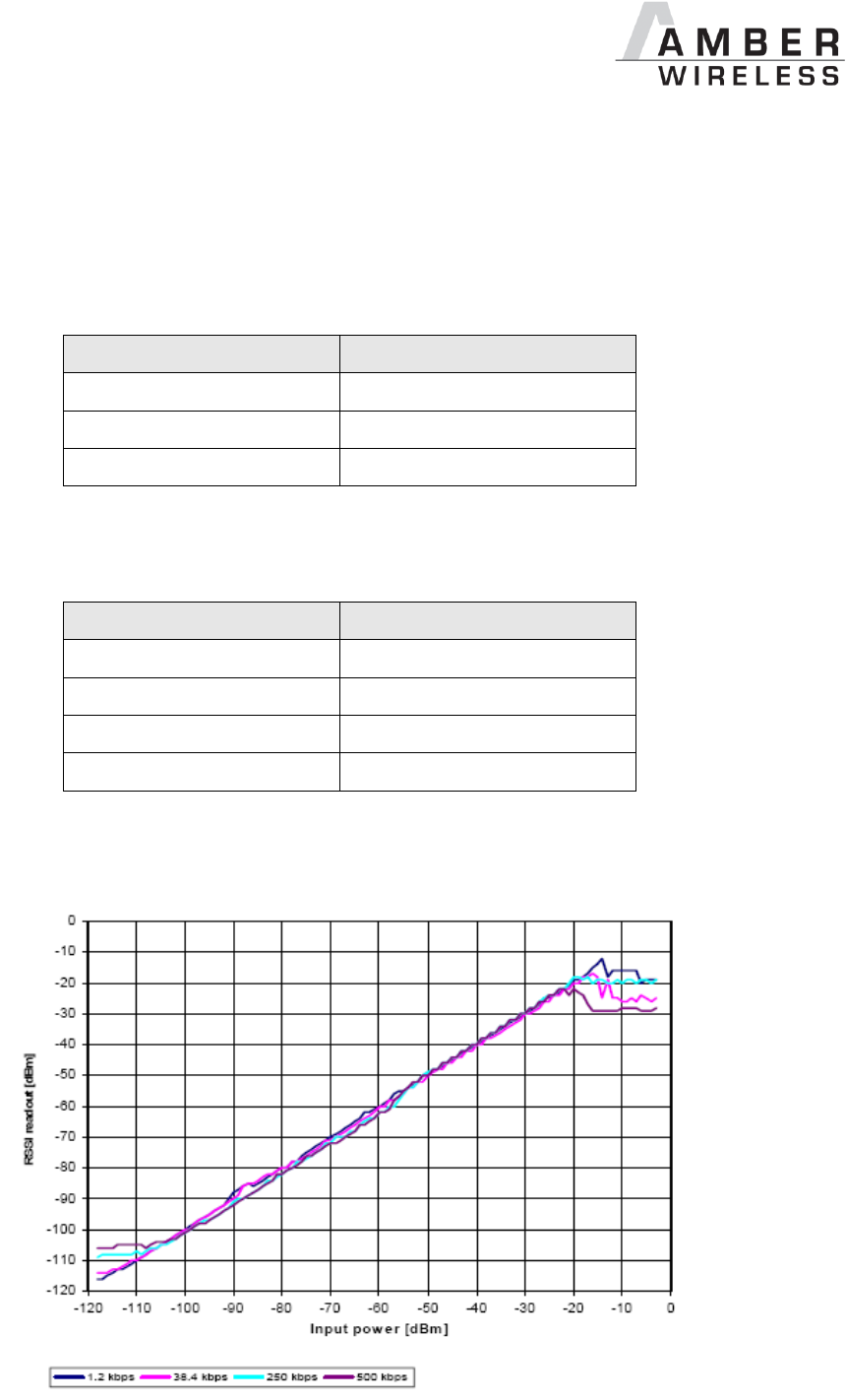
AMB8420_2524_2561_MA_V4_2 Page 19 of 61 Date: 12/2017
3. Otherwise (RSSIdec < 128): RSSIdBm = RSSIdec / 2 - RSSIOffset
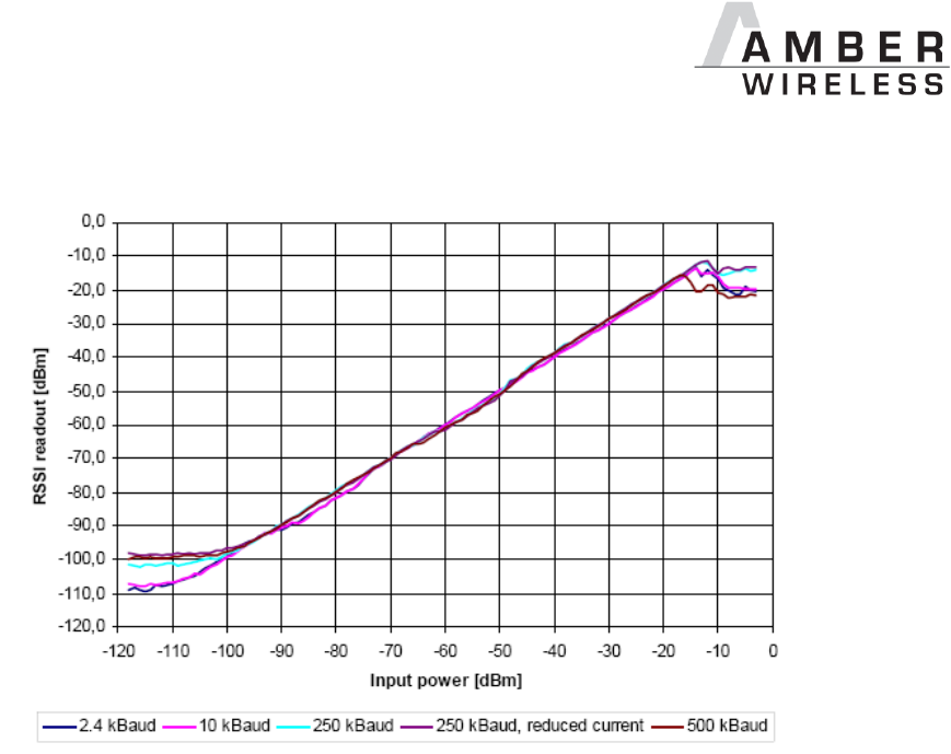
RSSIOffset is a data-rate-dependent correction factor according to Table 4 (AMB8420) and Table
5 (AMB2524).
The relation between the calculated value and the physical RX level in dBm is not linear across
the entire operating range and is displayed in Figure 2 and Figure 3 .
Data rate
RSSI offset
1.2 kbps
74
38.4 kbps
74
250 kbps
78
Table 4 Data rate-dependent RSSI offset for AMB8420 (from
[2])
Data rate
RSSI offset
2.4 kbps
71
10 kbps
69
250 kbps
72
500 kbps
72
Table 5 Data rate-dependent RSSI offset for AMB2524 (from
[3])
Figure 2 Relation between the RX level and the RSSI value read out for AMB8420 (from [2])
AMB8420_2524_2561_MA_V4_2 Page 20 of 61 Date: 12/2017
Figure 3 Relation between the RX level and the RSSI value read out for AMB2524 (from [3])
9.2.4 CMD_ERRORFLAGS_REQ
This command returns internal error states.
Format:
0x02 0x0E 0x00 0x0C
Return:
0x02 0x4E 0x02 < error flags MSB > < error flags LSB >< CS >
An error flag return value of "0" indicates that no error has occurred. The value is set back after
the query and in the event of a reset.
The meaning of the error flags is not described in detail in this context.

AMB8420_2524_2561_MA_V4_2 Page 21 of 61 Date: 12/2017
9.3 Modification of volatile parameters
This group contains all functions that will modify runtime settings while the module is running.
These settings are all volatile and will be reset to defaults on a reset of the module.
9.3.1 CMD_SET_MODE_REQ
This command is used to toggle the operating mode, e.g. to exit the command mode (this is
currently the only application). The return value will also be used as a start up indication if
OpMode is set to 0x10 or if a change of the mode using the /config pin was requested (when
changing into command mode).
Format:
0x02 0x04 0x01 < desired operating mode > < CS >
Example (exit command mode):
0x02 0x04 0x01 0x00 0x07
Return:
0x02 0x44 0x01 < newly configured operating mode > < CS >
Return for above example:
0x02 0x44 0x01 0x00 0x47
The following operating modes are defined:
Mode 0 (0x00): transparent data transfer
Mode 16 (0x10): command mode
9.3.2 CMD_SET_CHANNEL_REQ
This command is used to toggle the wireless channel. Unlike the non-volatile parameter
PHY_DefaultChannel (see 10.21), this is a volatile runtime parameter.
Format:
0x02 0x06 0x01 < 1-byte channel > < CS >
Example (selection of channel 108):
0x02 0x06 0x01 0x6C 0x69
Return:
0x02 0x46 0x01 < new channel > < CS >
Return for above example:
0x02 0x46 0x01 0x6C 0x29
The number of the newly set channel is returned. If the permissible frequency range is
exceeded, the lowest and highest permissible channels are configured and returned.
9.3.3 CMD_SET_DESTNETID_REQ
This command serves to configure the destination network ID in addressing mode 2. Unlike the
non-volatile parameter MAC_DestNetID, this is a volatile runtime parameter.

AMB8420_2524_2561_MA_V4_2 Page 22 of 61 Date: 12/2017
Format:
0x02 0x07 0x01 < 1-byte destination network ID > < CS >
Return:
0x02 0x47 0x01 < status > < CS >
Status:
0x00: success
9.3.4 CMD_SET_DESTADDR_REQ
This command serves to configure the destination address in addressing modes 1 and 2. Unlike
the non-volatile parameter MAC_DestAddrLSB (see 10.15), this is a volatile runtime
parameter.
Format:
0x02 0x08 0x01 < 1-byte destination address > < CS >
Return:
0x02 0x48 0x01 < status> < CS >
Status:
0x00: success

AMB8420_2524_2561_MA_V4_2 Page 23 of 61 Date: 12/2017
9.4 Modification of non-volatile parameters
The non-volatile parameters are also called user settings and are stored in a special flash
location.
9.4.1 CMD_SET_REQ
This command enables direct manipulation of the parameters in the module’s non-volatile
memory. The respective parameters are accessed by means of the memory position described
in Table 6. Access outside these memory positions is not possible by means of this function.
You can modify individual or multiple consecutive parameters in the memory at the same time.
Parameters of 2 or more bytes have to be transferred LSB first. The list and description of all
accessible non volatile parameters follows in chapter 9.4.2.
A CMD_SET_REQ shall always be preceded by a CMD_GET_REQ to check whether any
parameter needs a change. This is recommended to reduce the number erase-cycles on the
flash which are as a matter of fact limited.
Caution: The validity of the specified parameters is not verified. Incorrect values can
result in device malfunction!
Caution: To save the parameters in the flash memory of the module, the particular
memory segment must first be flushed entirely and then restored from the RAM. If a
reset occurs during this procedure (e.g. due to supply voltage fluctuations), the
entire memory area may be destroyed. In this case, the module may no longer be
operable, which means that the firmware must be re-installed via "ACC".
Recommendation: First verify the configuration of the module with CMD_GET_REQ;
write only if necessary.
Format:
0x02 0x09 < number of bytes + 2 > < memory position > < number of bytes > <
parameter > < CS >
Return:
0x02 0x49 0x01 < status > < CS >
Status:
0x00: success
0x01: invalid memory position (write access to unauthorised area > 79 / 0x4F)
0x02: invalid number of bytes to be written (write access to unauthorised area > 0x4F)
Example 1: Setting the number of wireless retries (parameter MAC_NumRetrys, memory
position 20 according to Table 6):
0x02 0x09 0x03 0x14 0x01 < MAC_NumRetrys > < CS >
Example 2: Setting the 3 registers for the baud rate configuration (UART_MCTL, UART_BR0,
and UART_BR1). According to Table 6, UART_MCTL has the memory position 2:
0x02 0x09 0x05 0x02 0x03 < UART_MCTL > < UART_BR0 > < UART_BR1 > < CS >

AMB8420_2524_2561_MA_V4_2 Page 24 of 61 Date: 12/2017
9.4.2 CMD_GET_REQ
This command can be used to query individual or multiple non-volatile parameters (see 9.4).
The requested number of bytes starting from the specified memory position are returned.
You can query individual or multiple consecutive parameters in the memory at the same time.
Parameters consisting of 2 or more bytes will typically be transferred LSB first order.
Format:
0x02 0x0A 0x02 < memory position > < number of bytes > < CS >
Example (query of all parameters):
0x02 0x0A 0x02 0x00 0x80 0x8A
Return:
0x02 0x4A < number of bytes + 2 > < memory position > < number of bytes > <
parameter > < CS >
Write or Read access to the memory area after the parameters documented in Table 6 is
blocked. The memory position and the number of bytes are limited accordingly. Thus, the last
memory position that can be read out is 79 (0x4F).

AMB8420_2524_2561_MA_V4_2 Page 25 of 61 Date: 12/2017
10 User settings
The non-volatile parameters listed in the following table can be modified by means of specific
commands in the configuration mode (CMD_SET_REQ, see 9.4) of the module or by using the
Windows software "ACC". These parameters are stored permanently in the module's flash
memory.
Caution: The validity of the specified parameters is not verified. Incorrect values can
result in device malfunction!
Designation
Designation in ACC
Summary
Permissible
values
Default
AMB8420
/
AMB2524
Memory
position
Number
of bytes
UART_CTL
Data format
Control register for
UART data format
See
description
16
0
1
UART_TCTL
Control register for
the baud rate (change
only after
consultation)
32
32
1
1
UART_MCTL
MCTL
Control register for
fine-adjusting the
UART baud rate;
concerning the
calculation, see [1]
0 - 255
0 / 68
2
1
UART_BR0
BR0
Prescaler for setting
the baud rate (LSB);
concerning the
calculation, see [1]
0 - 255
113 / 156
3
1
UART_BR1
BR1
Prescaler for setting
the baud rate (MSB);
concerning the
calculation, see [1]
0 - 255
2 / 0
4
1
UART_PktMode
Packetizing mode
Selects the packet
generation method
0 or 1
0
5
1
UART_PktSize
Packet size
Number of characters
for transmission start
with set packet size
1 - 128
128
7
1
UART_RTSLimit
/RTS limit
Number of received
characters after which
/RTS responds
1 - 128
112
8
1
UART_ETXChar
ETX character
End-of-text character
used to mark data
packets; reception of
this character triggers
wireless transmission
0 - 255
10
9
1

AMB8420_2524_2561_MA_V4_2 Page 26 of 61 Date: 12/2017
Designation
Designation in ACC
Summary
Permissible
values
Default
AMB8420
/
AMB2524
Memory
position
Number
of bytes
UART_Timeout
Timeout
Timeout after the last
character before the
data received via
UART are transmitted
via wireless
transmission (in
milliseconds)
0 – 65535
5
12
2
UART_DIDelay
Data indication delay
Delay between the
signalling by the
/DATA_INDICATION
pin and the start of
the output via UART
0 – 65535
0
14
2
MAC_NumRetrys
Retrys
Number of wireless
retries
0 – 255
0
20
1
MAC_AddrMode
Addressing mode
Addressing mode to
use
0/1/2
0
21
1
MAC_DestNetID
Dest. net ID
Default destination
network ID
0 – 255
0
24
1
MAC_DestAddrLSB
Dest. device address
Default destination
address (LSB)
0 – 255
0
25
1
MAC_SourceNetID
Local net ID
Own network ID
0 – 254
0
28
1
MAC_SourceAddrLSB
Local device address
Own address (LSB)
0 – 254
0
29
1
MAC_ACKTimeout
ACK timeout
Waiting time for
wireless
acknowledgement in
milliseconds
0 – 65535
10
32
2
PHY_FIFOPrecharge
FIFO precharge
Fill level of the FIFO
before the
transmission is
launched (change
only after
consultation)
8 – 64
8
40
1
PHY_PAPower
PA power
Transmission output;
value range depends
on HF configuration
0 - 255
195 3/
255
41
1
PHY_DefaultChannel
Default channel
Utilised wireless
channel after reset;
value range depends
on HF configuration
0 - 255
106 / 79
42
1
3
AMB8420 default 195, AMB8420-2 default 80

AMB8420_2524_2561_MA_V4_2 Page 27 of 61 Date: 12/2017
Designation
Designation in ACC
Summary
Permissible
values
Default
AMB8420
/
AMB2524
Memory
position
Number
of bytes
PHY_CCARSSILevel
CCA RSSI level
Field strength level
for "channel free"
detection (not yet
supported)
0 - 255
0
43
1
OpMode
Mode
Operating mode
0.16
0
60
1
MSP_RSELx
DCO resistor sel.
Start value for control
loop DCO calibration
after system reset
(change only after
consultation)
0 - 7
7
61
1
MSP_DCOCTL
DCO control
Start value for control
loop DCO calibration
after system reset
(change only after
consultation)
0 - 255
110
62
1
WOR_Prescaler
Prescaler
Duration of a wake-up
cycle for periodic
wake-ups in WOR
mode
0 – 65535
4096
64
2
WOR_Countdown
Countdown
Number of wake-up
cycles before waking
up in WOR mode
0 – 65535
5
66
2
WOR_RXOnTime
RX on time
Duration of RX
readiness in WOR
mode
0 – 65535
1000
68
2
CfgFlags
Configuration flags (hex.)
Flags for setting
various properties;
see 10.29
0 – 65535
0
(0x0000)
72
2
Synch1
Synch1
Synch word MSB for
transceiver (change
only after
consultation!)
0 - 255
211
76
1
Synch0
Synch0
Synch word LSB for
transceiver (change
only after
consultation)
0 - 255
145
77
1
Table 6 Overview of non-volatile configuration parameters

AMB8420_2524_2561_MA_V4_2 Page 28 of 61 Date: 12/2017
10.1 UART_CTL
The UART data format can be configured with the help of the upper 4 bits in this register. The
meaning of these bits is described in Table 7.
Bit no.
Description
0 to 3 (0x0F)
Reserved, must always be set to 0.
4 (0x10)
If this bit is set, the character length will be 8 bits, if not, it will
be 7 bits.
5 (0x20)
This bit selects the number of stop bits. If this bit is set, 2 stop
bits will be used, if not, 1 will be used.
6 (0x40)
If this bit is set, even parity will be used, if not, odd parity will
be used. This bit is only used if bit 7 is set to ‘1’.
7 (0x80)
This bit enables the use of parity (if set).
Table 7 Setting the data format
10.2 UART_TCTL
This register selects the source for generating the UART clock speed. Currently, the only
permissible value is 32.
10.3 UART_MCTL
The registers UART_MCTL, UART_BR0, and UART_BR1 can be used to set the UART baud
rate. Concerning the calculation of the corresponding settings, see [1].
10.4 UART_BR0
The registers UART_MCTL, UART_BR0, and UART_BR1 can be used to set the UART baud
rate. Concerning the calculation of the corresponding settings, see [1].
10.5 UART_BR1
The registers UART_MCTL, UART_BR0, and UART_BR1 can be used to set the UART baud
rate. Concerning the calculation of the corresponding settings, see [1]
10.6 UART_PktMode
Selects the method used for generating packets for the transparent operating mode. Two
methods have been implemented:
0. Mode 0: Sends when

AMB8420_2524_2561_MA_V4_2 Page 29 of 61 Date: 12/2017
a. the timeout defined with UART_Timeout is reached, or
b. the number of bytes defined with UART_PktSize is reached, or
c. the transmission of the data is requested by means of the /DATA_REQUEST pin.
1. Mode 1: Sends when
a. the character defined with UART_ETXChar is detected, or
b. the number of bytes defined with UART_PktSize has been received, or
c. the transmission of the data is requested by means of the /DATA_REQUEST pin.
Not used in the command mode.
10.7 UART_PktSize
Maximum number of bytes after which the wireless transmission of the data received via UART
starts. Used in packet mode 0 as well as in packet mode 1.
Not used in the command mode.
10.8 UART_RTSLimit
Number of bytes after which the host system is prompted to interrupt the data transfer over
/RTS. Necessary, because an immediate response to the /RTS signal may not take place
(UART FIFO), depending on the host system.
10.9 UART_ETXChar
End-of-text character that triggers the transmission of the data received via UART. Only used in
packet mode 1. During the wireless transmission, the ETX character is treated like a normal
character.
Not used in the command mode.
10.10 UART_Timeout
Timeout in milliseconds after the last character has been received on UART before the wireless
transmission of the data received via UART starts. Only used in packet mode 0.
In command mode, start of transmission is triggered by the well defined end of the command.
The parameters UART_Timeout is used in this case to define the maximum delay between two
consecutive characters. If this delay is reached (after detection of the STX character), the input
buffer will be flushed.
10.11 UART_DIDelay
This parameter determines the delay in milliseconds between the signalling of incoming
wireless data over the /DATA_INDICATION pin and the output of the data via UART. For
example, this delay can be used to prepare a "sleeping" host system for receiving the data.
From software version 3.2 also valid in the command mode.

AMB8420_2524_2561_MA_V4_2 Page 30 of 61 Date: 12/2017
10.12 MAC_NumRetrys
Determines the maximum number of wireless transmission retries. If this parameter is set to a
value other than 0, the receiver module will automatically be prompted to send a wireless
acknowledgement.
10.13 MAC_AddrMode
The following addressing modes are available:
1. No addressing (mode 0): Each module receives the transmitted HF telegram and
delivers the received data to the host system via UART. No address information is
transmitted in the wireless telegram.
2. 1-byte address (mode 1): The receiving module will only deliver the data to the host
system via UART if the destination address configured at the sender
(MAC_DestAddrLSB, see 10.15) corresponds to the source address
(MAC_SourceAddrLSB, see 10.17) or the address 255 (broadcast address) was
specified as destination address. Both the destination address and the source address
are transmitted in the wireless telegram (total = 2 bytes).
3. 2-byte address (mode 2): The receiving module will only deliver the data to the host
system via UART if both the destination network ID and the destination address
correspond to the source addresses (MAC_SourceNetID and
MAC_SourceAddrLSB, see 10.16 and 10.17) or the broadcast address 255 was
specified as destination address. A total of 4 bytes of address information are
transmitted in the wireless telegram.
Caution: The receiver and transmitter modules must be operated in the same
addressing mode!
Caution: In addressing mode 0, the use of wireless acknowledgement may cause
problems if several wireless modules are addressed simultaneously. In this case, all
modules will simultaneously acknowledge the receipt of the package. Thus, the
wireless acknowledgement cannot be received by the sending module due to the
collision, and the maximum number of retries will be sent.
10.14 MAC_DestNetID
Destination network address to use in addressing mode 2 after a reset. Can be modified with
the command CMD_SET_DESTNETID_REQ at runtime (volatile). If the special broadcast ID
and the broadcast address are set to 255, the sender will be received by all.
10.15 MAC_DestAddrLSB
Destination address to use in addressing modes 1 and 2 after a reset. Can be modified with the
command CMD_SET_DESTADDRESS_REQ at runtime (volatile). If the special broadcast

AMB8420_2524_2561_MA_V4_2 Page 31 of 61 Date: 12/2017
address is set to 255 (in the case of addressing mode 2, broadcast ID also 255), the sender will
be received by all.
10.16 MAC_SourceNetID
Source network ID in addressing mode 2.
10.17 MAC_SourceAddrLSB
Source device address in addressing modes 1 and 2.
10.18 MAC_ACKTimeout
Time to wait for a wireless acknowledgement before a wireless retry is triggered. The values are
automatically set in "ACC" depending on the configured HF data rate.
HF data rate
ACK timeout recommended
1.2 kbps
85 ms
2.4 kbps
45 ms
4.8 kbps
25 ms
10.0 kbps
15 ms
38.4 kbps
8 ms
76.8 kbps
6 ms
100.0 kbps
5 ms
250.0 kbps
5 ms
Table 8 Recommended timeouts
10.19 PHY_FIFOPrecharge
Number of bytes that are stored in the transceiver FIFO before actual transmission is launched.
Required to prevent a buffer underrun for HF baud rates of more than 200 kbps. The values are
automatically set in "ACC" depending on the configured HF data rate.
10.20 PHY_PAPower
HF output of the module. The maximum permissible output depends on the utilised HF
configuration. The default value already represents the maximum possible output.
10.21 PHY_DefaultChannel
Determines the wireless channel to use after a module reset.

AMB8420_2524_2561_MA_V4_2 Page 32 of 61 Date: 12/2017
10.22 PHY_CCARSSILevel
Field strength used for "channel-free" detection (not implemented).
10.23 OpMode
Operating mode to be used after power up. Modes 0 (transparent data transfer) and 16
(command mode) can be selected here.
10.24 MSP_RSELx
Start value for a register used to set the processor speed. The speed is controlled continuously
in the background. The frequency of the clock quartz is used for the calibration. The system
start-up time can be optimised by means of a suitable configuration of this register (change only
after consultation).
10.25 MSP_DCOCTL
Start value for a register used to set the processor speed. The speed is controlled continuously
in the background. The frequency of the clock quartz is used for the calibration. The system
start-up time can be optimised by suitably configuring this register (change only after
consultation).
10.26 WOR_Prescaler
Defines the intervals in which the module in the sleep mode wakes up for a countdown
(WOR_Countdown) until actual RX readiness. The interval (in seconds) is calculated as
follows:
4096
Pr_
Pr
escalerWOR
Tescaler
10.27 WOR_Countdown
Number of prescaler cycles (countdown) until the module in the WOR mode enters the RX
state. The duration until automatic RX readiness is calculated as follows:
4096
Pr__ escalerWORNumCylesWOR
TWOR
10.28 WOR_RXOnTime
Defines the duration in milliseconds for which the module in the WOR is RX-ready after waking
up before it returns to the sleep mode.
10.29 CfgFlags
16-bit bit field in which the use of individual pins or signals can be disabled. Table 9 presents a
description of the respective flags.

AMB8420_2524_2561_MA_V4_2 Page 33 of 61 Date: 12/2017
Bit no.
Description
0 (0x0001)
If this bit is set, the function of the /CONFIG pin will be disabled.
Subsequently, the unit can no longer be switched to the
command mode via this pin.
1 (0x0002)
If this bit is set, the function of the /DATA_REQUEST pin will be
disabled. Subsequently, data can no longer be sent using this
pin.
2 (0x0004)
If this bit is set, the detection of the break signal on the UART
interface will be suppressed. Subsequently, the unit can no
longer be switched to the command mode by means of such a
signal.
3 (0x0008)
If this bit is set, the status of the SLEEP and TRX_DISABLE
pins will be ignored. Thus, the module can no longer be set to
the various power-saving modes via these pins.
4 (0x0010)
Reserved
5 (0x0020)
If this bit is set, any character will be accepted as valid
checksum in the command mode.
6 (0x0040)
Reserved
7 (0x0080)
If this bit is set, the address will not be resolved. The particular
module can be used as packet sniffer to monitor a wireless link
(from version 3.2).
9 to 15 (0xFF00)
Reserved
Table 9 Configuration flags
Warning: If both bit 0 and bit 2 are set, the module can no longer be set to the
configuration mode. In this case, access to the operating parameters is only
possible with the "ACC" program.

AMB8420_2524_2561_MA_V4_2 Page 34 of 61 Date: 12/2017
11 Device addressing and wireless monitoring
To connect several modules to networks or to send data to specific devices, the module
supports the so called address mode. The corresponding user setting parameter
MAC_AddrMode determines whether all modules in range, or all modules in a network or a
single module with a fixed address is supposed to receive a certain message.
The address resolution can be disabled ("packet sniffer") with bit 7 in the CfgFlags. A module
configured in this way will receive all data packets and forward them to the serial interface,
regardless of the addressing mode. In sniffer mode, the module does not send any
acknowledgement.
AMB8420_2524_2561_MA_V4_2 Page 35 of 61 Date: 12/2017
12 Radio parameters
The RF parameters (data rate, usable frequency range, etc.) can be configured with the PC
program "ACC". Depending on the configured data rate, it can also be used to change
additional non volatile parameters, e.g. MAC_ACKTimeout, PHY_DefaultChannel, or
PHY_FIFOPrecharge.
12.1 AMB8420
The following sections describe the permissible data rates and frequency ranges. In the factory
state, the HF data rate is 38.4 kbps.
Caution: There is no interception mechanism concerning the duty cycle.
The duty cycle is subject to regulations and is declared asratio expressed as a
percentage of te cumulative duration of transmissions Ton_cum within an observation
interval Tobs. DC = (Ton_cum/Tobs)Fobs on an observation bandwidth Fobs. Unless
otherwise specified, Tobs is 1 hour and the observation bandwidth Fobs is the
operational frequency band.
Caution: Due to the changes in the Radio Directive the Occupied Channel Width has
to be declared and a non overlapping channel spacing is required. This channel
spacing equals the OCW, following table last column.
12.1.1 "M" band
This frequency band ranges from 868.0 to 868.6 MHz (channel 100 to 112) and permits a 1%
duty cycle.
Channel
no.
\ data
rate
100
101
102
103
104
105
106
107
108
109
110
111
112
OCW/
kHz
4.8 kbps
868.00
868.05
868.10
868.15
868.20
868.25
868.30
868.35
868.40
868.45
868.50
868.55
868.60
100
10 kbps
868.00
868.05
868.10
868.15
868.20
868.25
868.30
868.35
868.40
868.45
868.50
868.55
868.60
100
38.4
kbps
868.00
868.05
868.10
868.15
868.20
868.25
868.30
868.35
868.40
868.45
868.50
868.55
868.60
100
76.8
kbps
868.00
868.05
868.10
868.15
868.20
868.25
868.30
868.35
868.40
868.45
868.50
868.55
868.60
200
100
kbps
868.00
868.05
868.10
868.15
868.20
868.25
868.30
868.35
868.40
868.45
868.50
868.55
868.60
250
Table 10 Channel table "M" band. Permissible channels are highlighted in green
Caution:
The maximum permitted output power for the AMB8420 corresponds to the
maximum possible PHY_PAPower setting. The maximum allowable output power for
the AMB8420-2 is 0 dBm.
Depending on the applied antenna other values may be allowable. Determining is the
effective radiated power.

AMB8420_2524_2561_MA_V4_2 Page 36 of 61 Date: 12/2017
12.2 AMB2524
In the factory state, the HF data rate is 250 kbps.
The module AMB2524 uses a channel spacing of approximately 500 kHz; the carrier frequency
can be determined with the following formula:
)500.0(5.2400][ ChannelC NMHzF
Here, the channels 0 to 165 are permissible. See Table 11 for an overview of usable
frequencies.
Caution: Avoid the channels/frequencies (2405 MHz + n x 13MHz) marked in red,
which merely provide a reduced range due to a property of the wireless IC.
Channel no.
Freq. [MHz]
Channel no.
Freq. [MHz]
Channel no.
Freq. [MHz]
Channel no.
Freq. [MHz]
0
2400.5
41
2421.0
82
2441.5
123
2462.0
1
2401.0
42
2421.5
83
2442.0
124
2462.5
2
2401.5
43
2422.0
84
2442.5
125
2463.0
3
2402.0
44
2422.5
85
2443.0
126
2463.5
4
2402.5
45
2423.0
86
2443.5
127
2464.0
5
2403.0
46
2423.5
87
2444.0
128
2464.5
6
2403.5
47
2424.0
88
2444.5
129
2465.0
7
2404.0
48
2424.5
89
2445.0
130
2465.5
8
2404.5
49
2425.0
90
2445.5
131
2466.0
9
2405.0
50
2425.5
91
2446.0
132
2466.5
10
2405.5
51
2426.0
92
2446.5
133
2467.0
11
2406.0
52
2426.5
93
2447.0
134
2467.5
12
2406.5
53
2427.0
94
2447.5
135
2468.0
13
2407.0
54
2427.5
95
2448.0
136
2468.5
14
2407.5
55
2428.0
96
2448.5
137
2469.0
15
2408.0
56
2428.5
97
2449.0
138
2469.5
16
2408.5
57
2429.0
98
2449.5
139
2470.0
17
2409.0
58
2429.5
99
2450.0
140
2470.5
18
2409.5
59
2430.0
100
2450.5
141
2471.0
19
2410.0
60
2430.5
101
2451.0
142
2471.5
20
2410.5
61
2431.0
102
2451.5
143
2472.0
21
2411.0
62
2431.5
103
2452.0
144
2472.5
22
2411.5
63
2432.0
104
2452.5
145
2473.0
23
2412.0
64
2432.5
105
2453.0
146
2473.5
24
2412.5
65
2433.0
106
2453.5
147
2474.0
25
2413.0
66
2433.5
107
2454.0
148
2474.5
26
2413.5
67
2434.0
108
2454.5
149
2475.0
27
2414.0
68
2434.5
109
2455.0
150
2475.5
28
2414.5
69
2435.0
110
2455.5
151
2476.0
29
2415.0
70
2435.5
111
2456.0
152
2476.5
30
2415.5
71
2436.0
112
2456.5
153
2477.0
31
2416.0
72
2436.5
113
2457.0
154
2477.5
32
2416.5
73
2437.0
114
2457.5
155
2478.0

AMB8420_2524_2561_MA_V4_2 Page 37 of 61 Date: 12/2017
Channel no.
Freq. [MHz]
Channel no.
Freq. [MHz]
Channel no.
Freq. [MHz]
Channel no.
Freq. [MHz]
33
2417.0
74
2437.5
115
2458.0
156
2478.5
34
2417.5
75
2438.0
116
2458.5
157
2479.0
35
2418.0
76
2438.5
117
2459.0
158
2479.5
36
2418.5
77
2439.0
118
2459.5
159
2480.0
37
2419.0
78
2439.5
119
2460.0
160
2480.5
38
2419.5
79
2440.0
120
2460.5
161
2481.0
39
2420.0
80
2440.5
121
2461.0
162
2481.5
40
2420.5
81
2441.0
122
2461.5
163
2482.0
164
2482.5
165
2483.0
Table 11 Frequency assignment AMB2524

AMB8420_2524_2561_MA_V4_2 Page 38 of 61 Date: 12/2017
13 Battery powered operation
By way of the SLEEP and TRX_DISABLE pins, the module can be set to various power-saving
operating states. These states are described below. Table 12 presents an overview of the
available options.
TRX_DISABLE low
TRX_DISABLE high
SLEEP low
Active mode, wireless and UART
communication possible
Stand-by, only UART
communication possible
SLEEP
high
WOR mode, module wakes up and
is ready to receive
Sleep mode, neither UART nor
wireless communication possible
Table 12 Power consumption control
13.1 Active mode
In this operating state, the module is permanently ready to receive and forward data via UART
or wireless transmission. The module will only switch to one of the other power-saving modes
after processing any pending data transmission, i.e. /RTS must be low.
13.2 Stand-by
In this operating state, the module's transceiver is disabled. Wireless reception is not possible,
but transmission of data is possible.
13.3 WOR mode
The module automatically wakes up at configurable intervals and remains ready to receive for a
configurable time. In this connection, refer to the parameters WOR_Prescaler,
WOR_Countdown, and WOR_RXOnTime (from 10.26).
13.4 Sleep mode
This is the module state with the lowest power consumption. Wireless and UART
communication are not possible. The module switches to one of the other operating modes
when it detects a falling edge on the SLEEP pin.
Concerning the power consumption in this operating mode, refer to the note in section 0.

AMB8420_2524_2561_MA_V4_2 Page 39 of 61 Date: 12/2017
14 Timing parameters
14.1 Reset behaviour
Following a reset, a low level on the /RTS pin signals that the module is ready for operation.
However, the level is only valid after the time required for the internal initialisation of the
processor (a couple of µs).
After this initialisation, /RTS is first set to high. Then the processor rate is calibrated on the basis
of the watch crystal. Only after this procedure is the module ready for operation.
14.1.1 Power-on reset
After setting the supply voltage and releasing the /RESET pin (if wired), the period until the
module is ready for operation greatly depends on the build time of the clock quartz. This
procedure may take up to 1 second; typical values range from 200 to 400 ms.
Recommended procedure: Check for low level on /RTS pin 2 ms after setting the prescribed
supply voltage. Subsequently, an additional 100 µs is required until readiness.
14.1.2 Reset via /RESET pin
To force a module restart by means of the /RESET pin, it must first be set to low for at least 10
ms.
After the pin is released, /RTS will switch to high after 100 µs at the latest. As the build-up time
for the clock quartz does not apply in this case, the time until the module is ready for operation
is reduced to a couple of ms. During this time, the processor rate will be calibrated, which takes
anywhere between 2 and 20 ms depending on the supply voltage and temperature.
Recommended procedure: After the /RESET pin is released, wait for 2 ms for low level on the
/RTS pin. Subsequently, an additional 100 µs are required until readiness.
14.2 Wake-up from the sleep mode
The switch-over to and from the sleep mode is also acknowledged via the /RTS signal.
Recommended procedure: After the SLEEP pin is released, wait for low level on the /RTS pin.
Subsequently, an additional 100 µs are required until readiness.
14.3 Latencies during data transfer / packet generation
The data transfer is always buffered, i.e. data received via UART is buffered in the module until
a specific event (see Table 2) occurs. Subsequently, the UART reception is interrupted (flow
control with /RTS signal), and the payload data is passed to the internal memory of the wireless
transceiver (FIFO).
The wireless transmission starts as soon as the first data is available in the transceiver memory;
during the ongoing wireless transmission, the remaining payload data is transmitted piece by
piece.
On the receiver side, the FIFO is read as soon as an incoming packet is detected.

AMB8420_2524_2561_MA_V4_2 Page 40 of 61 Date: 12/2017
In combination with a suitable packet generation method, this procedure enables the
minimisation of the latencies resulting from buffering.
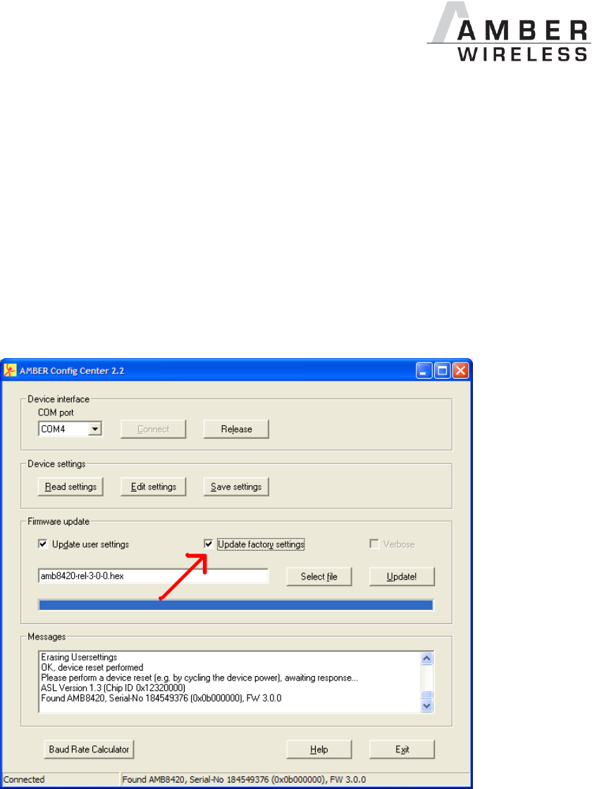
AMB8420_2524_2561_MA_V4_2 Page 41 of 61 Date: 12/2017
15 Firmware update
The firmware of the module can be updated with the PC utility "ACC" via the serial interface. If
the module is not connected to a PC, the UART of the module should be made accessible, e.g.
by means of suitable connectors. Only the UTDX and URXD signals are needed for this
procedure.
A level converter (TTL to RS232) is required for PC connection.
15.1 Update of earlier firmware versions (< 3.0.0)
To update firmware versions prior to 3.0.0, activate the option "Update factory settings" when
using "ACC". This approach ensures that the new parameters added to the factory settings of
the module are also overwritten. See Figure 4.
Figure 4 Firmware update for versions < 3.0.0

AMB8420_2524_2561_MA_V4_2 Page 42 of 61 Date: 12/2017
16 Firmware history
Version 3.0
Product release
Version 3.1
Bug fix "break detection"
Version 3.2
Bug fix UART_DIDelay in command mode
Sniffer mode via CfgFlags
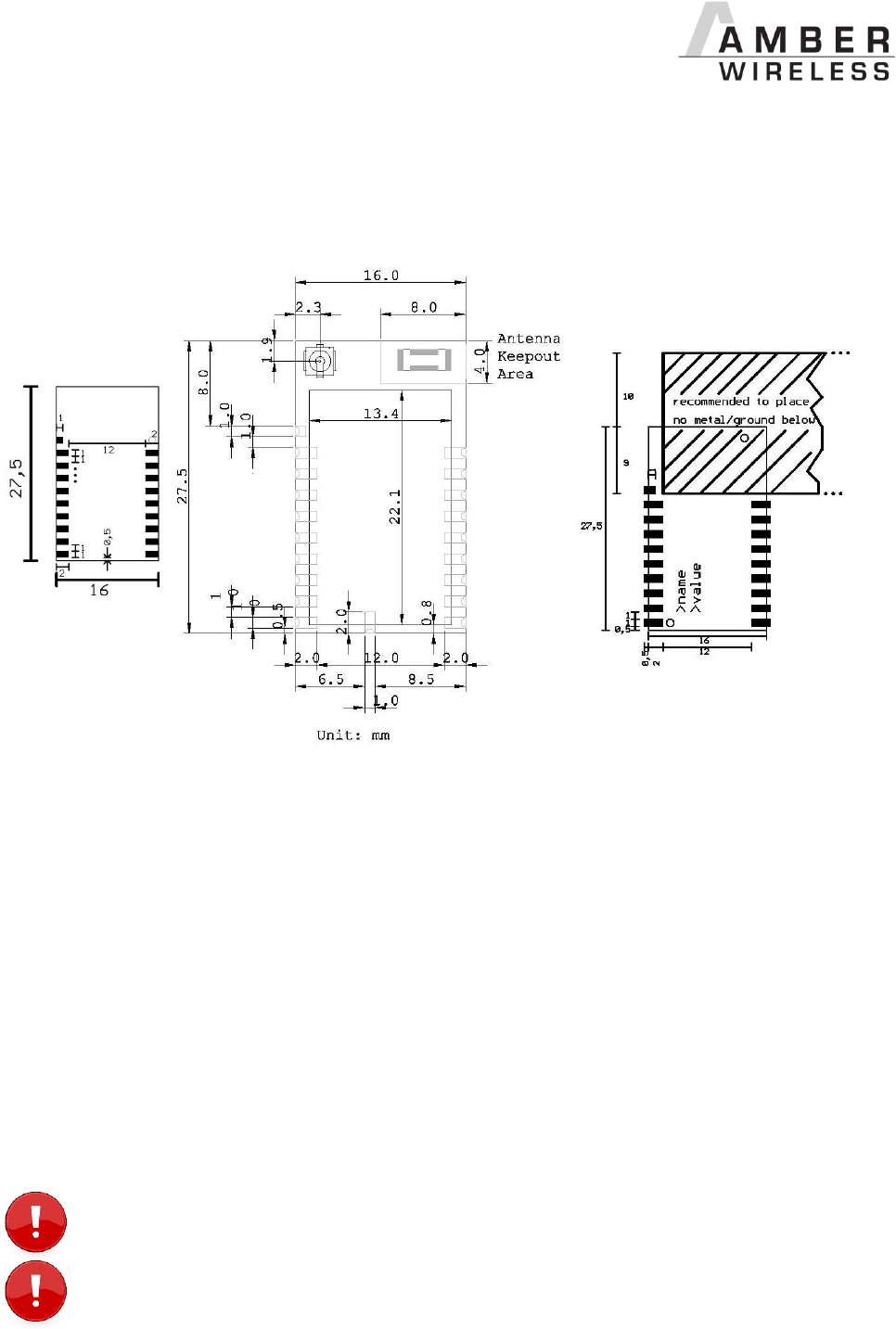
AMB8420_2524_2561_MA_V4_2 Page 43 of 61 Date: 12/2017
17 Manufacturing information
17.1 Footprint dimensioning proposal
Figure 5
Dimensional
drawing AMB8420
Figure 6
Dimensional drawing AMB2524
Figure 7
Proposal for footprint
Dimensions in mm. When designing the carrier board layout for AMB8420/AMB2524 the
following must be taken into consideration:
As shown in Figure 7, avoid having any ground or metal in the ceramic antenna area
(none at all on the right side and at least 10 mm distance above if it cannot be avoided).
The top layer of the carrier board should be kept free of tracks/vias underneath the
AMB8420/AMB2524, as it is merely coated with solder mask (unspecified insulation
properties) and the bottom of the AMB8420/AMB2524 has uncovered vias.
Tracks should only be laid under the AMB8420 in multi-layer structures in which layer 2
serves as ground layer that shields the underlying layers.
Caution: If the spacing of 12 mm between the pad rows is not complied with, there
will be a substantial short-circuit risk of VCC against GND!
Caution: The not described Pads, three Pads underneath the AMB8420 and the Pad
at the AMB2524 facing away from the antenna are only for manufacturing process
and must not be connected.
AMB8420_2524_2561_MA_V4_2 Page 44 of 61 Date: 12/2017
18 Design in Guide
18.1 Advice for Schematic and Layout
For users with less RF experience it is advisable to closely copy the relating evaluation board
with respect to schematic and layout, as it is a proven design. The layout should be conducted
with particular care, because even small deficiencies could affect the radio performance and its
range or even the conformity.
The following general advice should be taken into consideration:
A clean power supply is strongly recommended. Interference, especially oscillation can
severely restrain range and conformity.
Variations in voltage level should be avoided.
LDOs, properly designed in, usually deliver a proper regulated voltage.
Blocking capacitors and a ferrite bead in the power supply line can be included to filter
and smoothen the supply voltage when necessary.
No fixed values can be recommended, as these depend on the circumstances of the
application (main power source, interferences etc.).
Frequently switching the module on and off, especially with a slowly changing voltage
level of the power supply, can lead to erratic behavior, in rare cases even as far as
damaging the module or the firmware. The use of an external reset IC can solve this
matter.
Elements for ESD protection should be placed on all Pins that are accessible from the
outside and should be placed close to the accessible area. For example, the RF-Pin is
accessible when using an external antenna and should be protected.
ESD protection for the antenna connection must be chosen such as to have a minimum
effect on the RF signal. For example, a protection diode with low capacitance such as
the LXES15AAA1-100 or a 68 nH air-core coil connecting the RF-line to ground give
good results.
Placeholders for optional antenna matching or additional filtering are recommended.
The antenna path should be kept as short as possible.
Again, no fixed values can be recommended, as they depend on the influencing
circumstances of the application (antenna, interferences etc.).
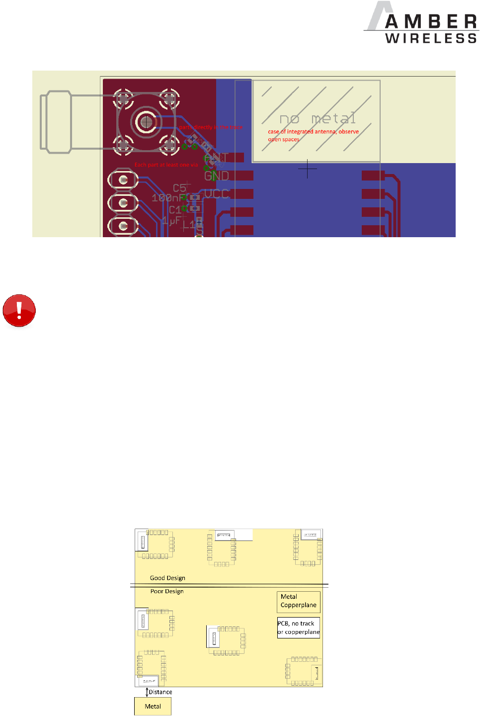
AMB8420_2524_2561_MA_V4_2 Page 45 of 61 Date: 12/2017
Figure 8: Layout
To avoid the risk of short circuits and interference there should be no routing underneath
the module on the top layer of the baseboard.
On the second layer, a ground plane is recommended, to provide good grounding
and shielding to any following layers and application environment.
In case of integrated antennas it is required to have areas free from ground. This area
should be copied from the evaluation board.
The area with the integrated antenna must overlap with the carrier board and should not
protrude, as it is matched to sitting directly on top of a 1.5 mm thick PCB.
Modules with integrated antennas should be placed with the antenna at the edge of the
main board. It should not be placed in the middle of the main board or far away from the
edge. This is to avoid tracks beside the antenna.
Filter and blocking capacitors should be placed directly in the tracks without stubs, to
achieve the best effect.
Antenna matching elements should be placed close to the antenna / connector, blocking
capacitors close to the module.
Ground connections for the module and the capacitors should be kept as short as
possible and with at least one separate through hole connection to the ground layer.
ESD protection elements should be placed as close as possible to the exposed areas.
Figure 9: Placement of the module with integrated antenna
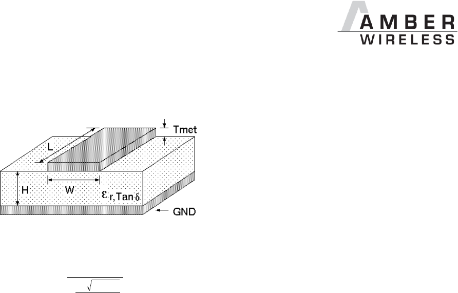
AMB8420_2524_2561_MA_V4_2 Page 46 of 61 Date: 12/2017
18.2 Dimensioning of the 50 Ohm microstrip
The antenna track has to be designed as a 50 Ohm feed line.
Figure 10 Dimensioning the antenna feed line as micro strip
The width W for a micro strip can be calculated using the following equation:
met
T
e
H
Wr
87
41.150
98.5
25.1
Equation 1 Parameters of the antenna feeding line
Example: a FR4 material with r = 4.3, a height H = 1000 µm and a copper thickness of Tmet= 18
µm will lead to a trace width of W ~ 1.9 mm. To ease the calculation of the Microstrip line (or
e.g. a coplanar) many calculators can be found in the internet.
As rule of thumb a distance of about 3 x W should be observed between the micro strip
and other traces / ground.
The Microstrip refers to ground, therefore there has to be the ground plane underneath
the trace.
Keep the feeding line as short as possible.

AMB8420_2524_2561_MA_V4_2 Page 47 of 61 Date: 12/2017
18.3 Antenna solutions
There exist several kinds of antennas, which are optimized for different needs. Chip antennas
are optimized for minimal size requirements but at the expense of range, PCB antennas are
optimized for minimal costs, and are generally a compromise between size and range. Both
usually fit inside a housing. Range optimization in general is at the expense of space. Antennas
that are bigger in size, so that they would probably not fit in a small housing, are usually
equipped with a RF connector. A benefit of this connector may be to use it to lead the RF signal
through a metal plate (e.g. metal housing, cabinet).
As a rule of thumb a minimum distance of Lambda/10 (3.5 cm @ 868 MHz, 1.2 cm @ 2.44
GHz) from the antenna to any other metal should be kept. Metal placed further away will not
directly influence the behavior of the antenna, but will anyway produce shadowing.
Keep the antenna away from large metal objects as far as possible to avoid
electromagnetic field blocking.
In the following chapters, some special types of antenna are described.
18.3.1 Lambda/4 radiator
An effective antenna is a Lambda/4 radiator. The simplest realization is an 8.6 cm long piece of
wire for 868 MHz, respectively a 3.1 cm long piece of wire for 2.44 GHz. This radiator needs a
ground plane at its feeding point. Ideally, it is placed vertically in the middle of the ground plane.
As this is often not possible because of space requirements, a suitable compromise is to bend
the wire away from the PCB respective to the ground plane. The Lambda/4 radiator has
approximately 40 Ohm input impedance, therefore matching is not required.
18.3.2 Chip antenna
There are many chip antennas from various manufacturers. The benefit of a chip antenna is
obviously the minimal space required and reasonable costs. However, this is often at the
expense of range. For the chip antennas, reference designs should be followed as closely as
possible, because only in this constellation can the stated performance be achieved.
18.3.3 PCB antenna
PCB antenna designs can be very different. The special attention can be on the miniaturization
or on the performance. The benefits of the PCB antenna are their small / not existing (if PCB
space is available) costs, however the evaluation of a PCB antenna holds more risk of failure
than the use of a finished antenna. Most PCB antenna designs are a compromise of range and
space between chip antennas and connector antennas.
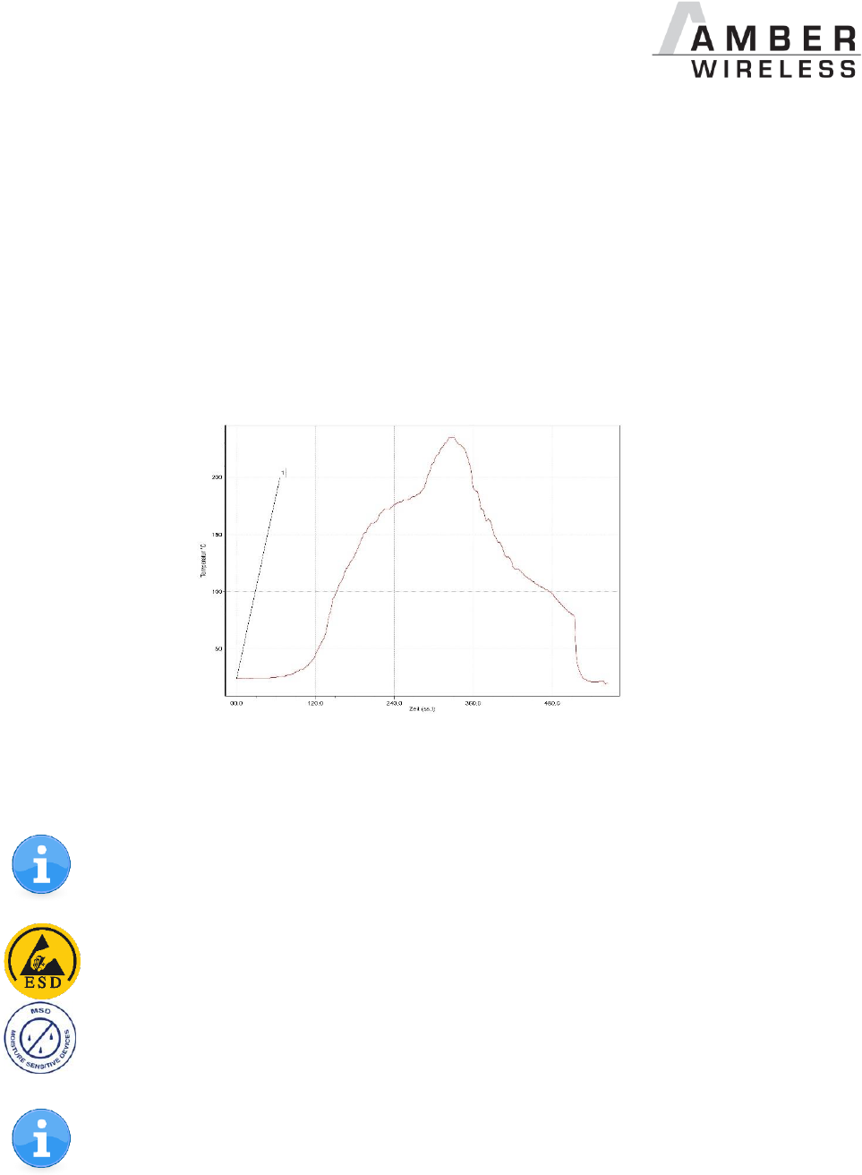
AMB8420_2524_2561_MA_V4_2 Page 48 of 61 Date: 12/2017
19 Manufacturing information
The assembly contains moisture sensitive devices of the MSL classification 3. Only the
dry packed Tape & Reel devices are suitable for the immediate processing in a reflow
process.
Further information concerning the handling of moisture sensitive devices, (e.g. drying)
can be obtained from the IPC/ JEDEC J-STD-033.
Recommendations for the temperature profile for the soldering furnace cannot be made,
as it depends on the substrate board, the number and characteristics of the
components, and the soldering paste used (consult your EMS).
Fehler! Verweisquelle konnte nicht gefunden werden.The following figure shows a soldering c
urve that had been used for a 31 cm2 carrier board for single-side assembly.
Figure 11 Example of a temperature profile
Caution: Must be adjusted to the characteristics of the carrier board!
To ensure the mechanical stability of the modules it is recommended to solder all
pads of the module to the base board, even if they are not used for the application.
Caution! ESD sensitive device.
Care should be taken when handling the device in order to prevent permanent
damage.
MSL 3
Caution! This assembly contains moisture sensitive components.
Care should be taken when processing the device according to IPC/JEDEC J-STD-
033.
Since the module itself is not fused the voltage supply shall be fed from a limited
power source according to clause 2.5 of EN 60950-1.

AMB8420_2524_2561_MA_V4_2 Page 49 of 61 Date: 12/2017
20 References
[1] To calculate the baud rate registers UART_MCTL, UART_BR0, and UART_BR1, the
"Baud Rate Calculator" tool is integrated in ACC. To configure a standard baud rate,
ACC provides a drop-down field with automatic calculation and parameterisation of the
baud rate registers.
[2] "CC1101 Single-Chip Low-Cost Low-Power RF Transceiver (Rev. B)", Texas
Instruments
[3] "CC2500 Single-Chip Low-Cost Low-Power RF Transceiver (Rev. B)", Texas
Instruments
[4] "AMB8420 Data Sheet", AMBER wireless GmbH
[5] "AMB2524 Data Sheet", AMBER wireless GmbH

AMB8420_2524_2561_MA_V4_2 Page 50 of 61 Date: 12/2017
21 Regulatory compliance information
21.1 AMB8420
21.1.1 Important notice
The use of RF frequencies is limited by national regulations. The AMB8420 has been designed
to comply with the Radio Equipment Directive 2014/53/EU of the European Union (EU). The
AMB8420 can be operated without notification and free of charge in the area of the European
Union. However, according to the RED, restrictions (e.g. in terms of duty cycle or maximum
allowed RF power) may apply.
Conformity assessment of the final product
The AMB8420 is a subassembly. It is designed to be embedded into other products (products
incorporating the AMB8420 are henceforward referred to as "final products").
It is the responsibility of the manufacturer of the final product to ensure that the final product is
in compliance with the essential requirements of the European Radio Equipment Directive.
The conformity assessment of the subassembly AMB8420 carried out by AMBER wireless
GmbH does not replace the required conformity assessment of the final product in accordance
to the RED.
Exemption clause
Relevant regulation requirements are subject to change. AMBER wireless GmbH does not
guarantee the accuracy of the before mentioned information. Directives, technical standards,
procedural descriptions and the like may be interpreted differently by the national authorities.
Equally, the national laws and restrictions may vary with the country. In case of doubt or
uncertainty, we recommend that you consult with the authorities or official certification
organizations of the relevant countries. AMBER wireless GmbH is exempt from any
responsibilities or liabilities related to regulatory compliance.
AMB8420_2524_2561_MA_V4_2 Page 51 of 61 Date: 12/2017
21.1.2 EU Declaration of conformity AMB8420

AMB8420_2524_2561_MA_V4_2 Page 52 of 61 Date: 12/2017
21.2 AMB2524
21.2.1 Important notice
The use of RF frequencies is limited by national regulations.
The AMB2524 has been designed to comply with the Radio Equipment Directive 2014/53/EU of
the European Union (EU). The AMB2524 can be operated without notification and free of
charge in the area of the European Union. However, according to the RED, restrictions (e.g. in
terms of duty cycle or maximum allowed RF power) may apply.
The AMB2524 has been designed to comply with the FCC and IC. The AMB2524 can be
operated without notification and free of charge in the area of USA and Canada.
Conformity assessment of the final product
The AMB2524 is a subassembly. It is designed to be embedded into other products (products
incorporating the AMB2524 are henceforward referred to as "final products").
It is the responsibility of the manufacturer of the final product to ensure that the final product is
in compliance with the essential requirements of the European Radio Equipment Directive, FCC
and IC.
The conformity assessment of the subassembly AMB2524 carried out by AMBER wireless
GmbH does not replace the required conformity assessment of the final product in accordance
to the RED.
Exemption clause
Relevant regulation requirements are subject to change. AMBER wireless GmbH does not
guarantee the accuracy of the before mentioned information. Directives, technical standards,
procedural descriptions and the like may be interpreted differently by the national authorities.
Equally, the national laws and restrictions may vary with the country. In case of doubt or
uncertainty, we recommend that you consult with the authorities or official certification
organizations of the relevant countries. AMBER wireless GmbH is exempt from any
responsibilities or liabilities related to regulatory compliance.
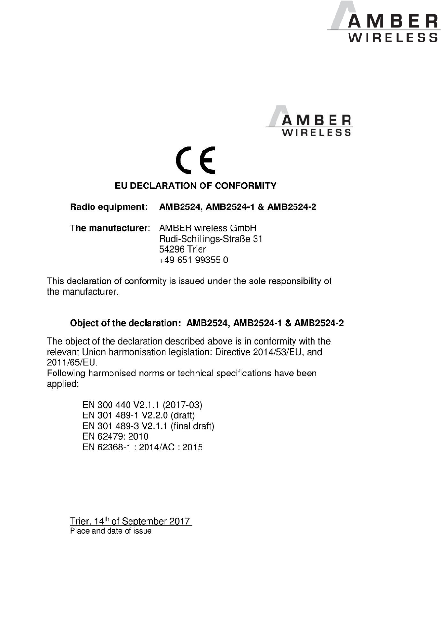
AMB8420_2524_2561_MA_V4_2 Page 53 of 61 Date: 12/2017
21.2.2 EU Declaration of conformity AMB2524

AMB8420_2524_2561_MA_V4_2 Page 54 of 61 Date: 12/2017
21.2.3 FCC Compliance statement AMB2524 & AMB2524-1
FCC ID: R7TAMB2524
This device complies with Part 15 of the FCC Rules.
Operation is subject to the following two conditions:
(1) this device may not cause harmful interference, and
(2) this device must accept any interference received, including interference that may cause
undesired operation.
(FCC 15.19)
Modifications (FCC 15.21)
Caution: Changes or modifications for this equipment not expressly approved by AMBER
wireless may void the FCC authorization to operate this equipment.
21.2.4 IC Compliance statement AMB2524 & AMB2524-1
Certification Number: 5136A- AMB2524
This device complies with Industry Canada licence-exempt RSS standard(s). Operation is
subject to the following two conditions: (1) this device may not cause harmful interference, and
(2) this device must accept any interference received, including interference that may cause
undesired operation.
Le présent appareil est conforme aux CNR d'Industrie Canada applicables aux appareils radio
exempts de licence. L'exploitation est autorisée aux deux conditions suivantes : (1) l'appareil ne
doit pas produire de brouillage, et (2) l'utilisateur de l'appareil doit accepter tout brouillage
radioélectrique subi, même si le brouillage est susceptible d'en compromettre le
fonctionnement.
21.2.5 FCC and IC Requirements to OEM integrators
This module has been granted modular approval. OEM integrators for host products may use
the module in their final products without additional FCC / IC (Industry Canada) certification if
they meet the following conditions. Otherwise, additional FCC / IC approvals must be obtained.
The host product with the module installed must be evaluated for simultaneous transmission
requirements.
The users manual for the host product must clearly indicate the operating requirements and
conditions that must be observed to ensure compliance with current FCC / IC RF exposure
guidelines.
To comply with FCC / IC regulations limiting both maximum RF output power and human
exposure to RF radiation, the maximum antenna gain including cable loss in a mobile-only
exposure condition must not exceed 2dBi.
A label must be affixed to the outside of the host product with the following statements:
This device contains FCCID: R7TAMB2524
This equipment contains equipment certified under ICID: 5136A-AMB2524

AMB8420_2524_2561_MA_V4_2 Page 55 of 61 Date: 12/2017
The final host / module combination may also need to be evaluated against the FCC Part 15B
criteria for unintentional radiators in order to be properly authorized for operation as a Part 15
digital device.
If the final host / module combination is intended for use as a portable device (see
classifications below) the host manufacturer is responsible for separate approvals for the SAR
requirements from FCC Part 2.1093 and RSS-102.
OEM Requirements:
The OEM must ensure that the following conditions are met.
End users of products, which contain the module, must not have the ability to alter the
firmware that governs the operation of the module. The agency grant is valid only when the
module is incorporated into a final product by OEM integrators.
The end-user must not be provided with instructions to remove, adjust or install the module.
The Original Equipment Manufacturer (OEM) must ensure that FCC labeling requirements
are met. This includes a clearly visible label on the outside of the final product. Attaching a
label to a removable portion of the final product, such as a battery cover, is not permitted.
The label must include the following text:
Contains FCC ID: R7TAMB2524
The enclosed device complies with Part 15 of the FCC Rules. Operation is subject to
the following two conditions: (i.) this device may not cause harmful interference and
(ii.) this device must accept any interference received, including interference that may cause
undesired operation.
When the device is so small or for such use that it is not practicable to place the statement
above on it, the information required by this paragraph shall be placed in a prominent location in
the instruction manual or pamphlet supplied to the user or, alternatively, shall be placed on the
container in which the device is marketed. However, the FCC identifier or the unique identifier,
as appropriate, must be displayed on the device.
The user manual for the end product must also contain the text given above.
Changes or modifications not expressly approved could void the user's authority to operate
the equipment.
The OEM must ensure that timing requirements according to 47 CFR 15.231(a-c) are met.
The OEM must sign the OEM Modular Approval Agreement with xxxxx
The module must be used with only the following approved antenna(s).
21.2.6 AMB2524 & AMB2524-1
The module variants HVIN AMB2524 and AMB2524-1 collected in the PMN AMB2524 are
identicall in enclosure, appearance, PCB design and bands/technologies.
The only difference is, that in AMB2524 an integrated Chip Antenna is used and for the
AMB2524-1 an external λ/4 Antenna is used.

AMB8420_2524_2561_MA_V4_2 Page 56 of 61 Date: 12/2017
21.3 AMB2561
21.3.1 Important notice
The use of RF frequencies is limited by national regulations. The AMB2561 has been designed
to comply with the Radio Equipment Directive 2014/53/EU of the European Union (EU). The
AMB2561 can be operated without notification and free of charge in the area of the European
Union. However, according to the RED, restrictions (e.g. in terms of duty cycle or maximum
allowed RF power) may apply.
Conformity assessment of the final product
The AMB2561 is a subassembly. It is designed to be embedded into other products (products
incorporating the AMB2561 are henceforward referred to as "final products").
It is the responsibility of the manufacturer of the final product to ensure that the final product is
in compliance with the essential requirements of the European Radio Equipment Directive.
The conformity assessment of the subassembly AMB2561 carried out by AMBER wireless
GmbH does not replace the required conformity assessment of the final product in accordance
to the RED.
Exemption clause
Relevant regulation requirements are subject to change. AMBER wireless GmbH does not
guarantee the accuracy of the before mentioned information. Directives, technical standards,
procedural descriptions and the like may be interpreted differently by the national authorities.
Equally, the national laws and restrictions may vary with the country. In case of doubt or
uncertainty, we recommend that you consult with the authorities or official certification
organizations of the relevant countries. AMBER wireless GmbH is exempt from any
responsibilities or liabilities related to regulatory compliance.
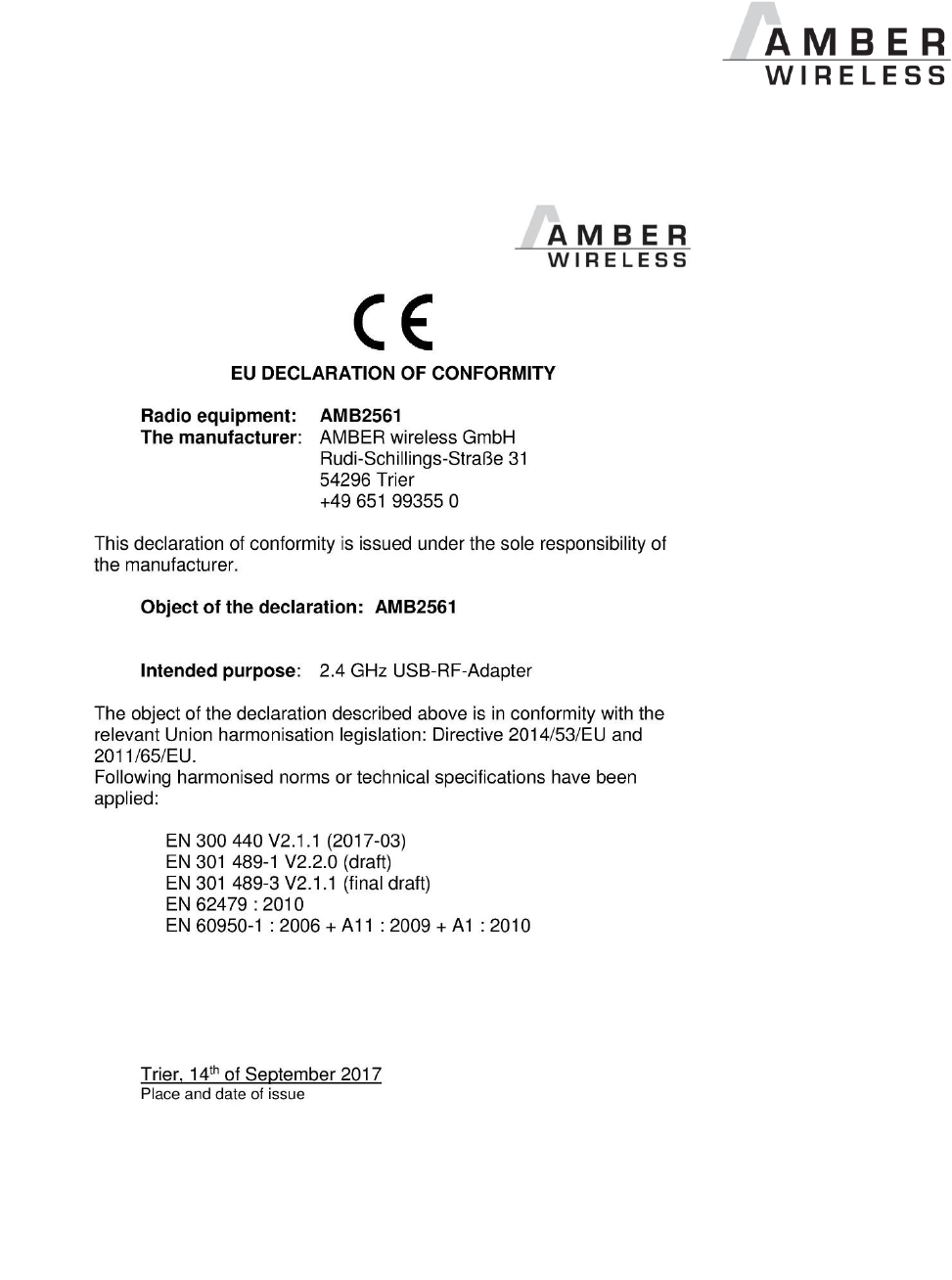
AMB8420_2524_2561_MA_V4_2 Page 57 of 61 Date: 12/2017
21.3.2 EU Declaration of conformity AMB2561

AMB8420_2524_2561_MA_V4_2 Page 58 of 61 Date: 12/2017
21.3.3 FCC statement
FCC ID: R7TAMB2561
This device complies with Part 15 of the FCC Rules. Operation is subject to the
following two conditions: (1) this device may not cause harmful interference, and (2)
this device must accept any interference received, including interference that may
cause undesired operation. (FCC 15.19)
Radio Frequency Interference (FCC 15.105)
This equipment has been tested and found to comply with the limits for Class B digital devices
pursuant to part 15 of the FCC Rules. These limits are designed to provide reasonable
protection against harmful interference in a residential installation. This equipment generates,
uses and can radiate radio frequency energy and, if not installed and used in accordance with
the instructions, may cause harmful interference to radio communications. However, there is no
guarantee that interference will not occur in a particular installation. If this equipment does
cause harmful interference to radio or television reception, which can be determined by turnin
the equipment off and on, the user is encouraged to try to correct the interference by one or
more of the following measures:
- Reorient or relocate the receiving antenna.
- Increase the separation between the equipment and receiver.
- Connect the equipment into an outlet on a circuit different from that to which the receiver
is connected.
- Consult the dealer or an experienced radio/TV technician for help.
Modifications (FCC 15.21)
Caution: Changes or modifications for this equipment not expressly approved by AMBER
wireless may void the user’s authority to operate this equipment.

AMB8420_2524_2561_MA_V4_2 Page 59 of 61 Date: 12/2017
21.4 AMB2520-4
21.4.1 Important notice
The use of RF frequencies is limited by national regulations. The AMB2520-4 has been
designed to comply with the Radio Equipment Directive 2014/53/EU of the European Union
(EU). The AMB2520-4 can be operated without notification and free of charge in the area of the
European Union. However, according to the RED, restrictions (e.g. in terms of duty cycle or
maximum allowed RF power) may apply.
Conformity assessment of the final product
The AMB2520-4 is a subassembly. It is designed to be embedded into other products (products
incorporating the AMB2520-4 are henceforward referred to as "final products").
It is the responsibility of the manufacturer of the final product to ensure that the final product is
in compliance with the essential requirements of the European Radio Equipment Directive.
The conformity assessment of the subassembly AMB2520-4 carried out by AMBER wireless
GmbH does not replace the required conformity assessment of the final product in accordance
to the RED.
Exemption clause
Relevant regulation requirements are subject to change. AMBER wireless GmbH does not
guarantee the accuracy of the before mentioned information. Directives, technical standards,
procedural descriptions and the like may be interpreted differently by the national authorities.
Equally, the national laws and restrictions may vary with the country. In case of doubt or
uncertainty, we recommend that you consult with the authorities or official certification
organizations of the relevant countries. AMBER wireless GmbH is exempt from any
responsibilities or liabilities related to regulatory compliance.
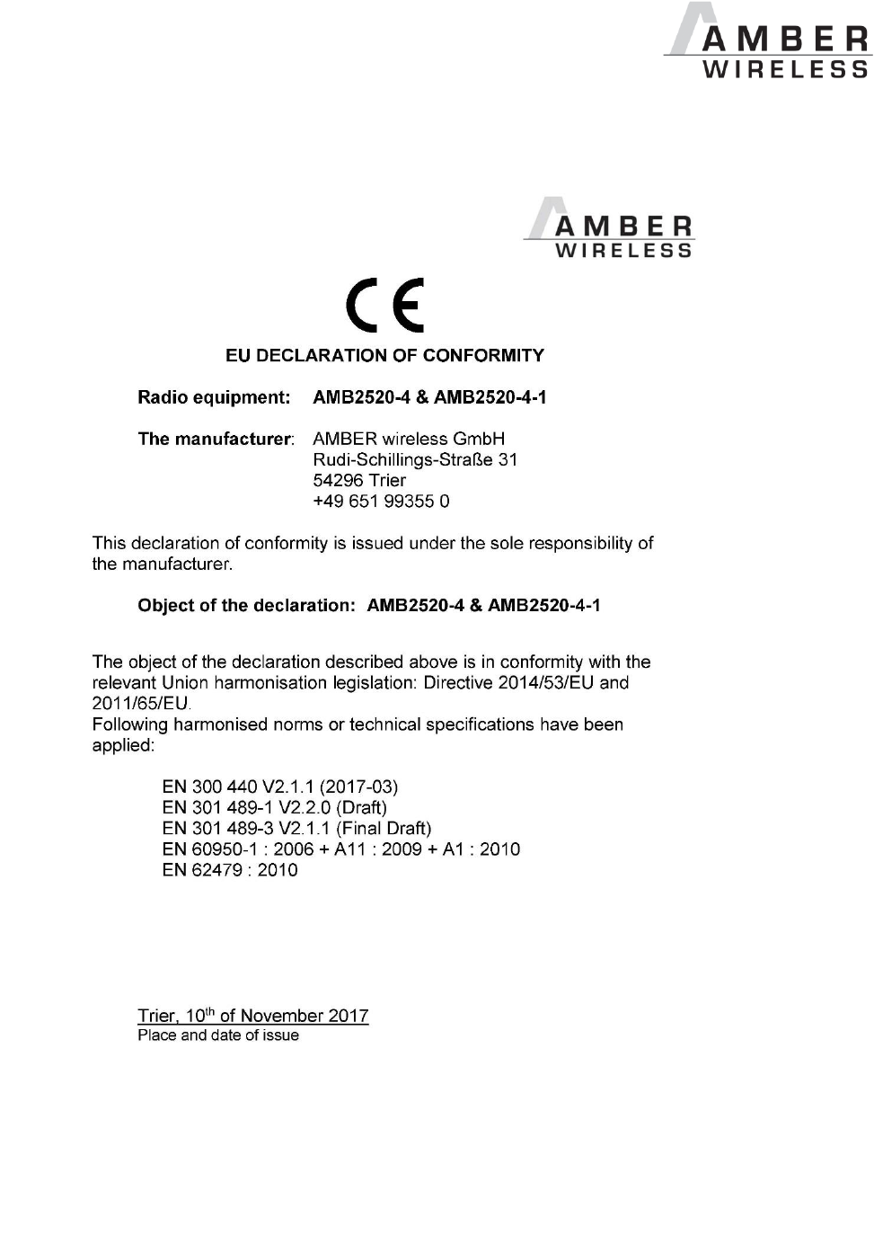
AMB8420_2524_2561_MA_V4_2 Page 60 of 61 Date: 12/2017
21.4.2 EU Declaration of conformity AMB2520-4

AMB8420_2524_2561_MA_V4_2 Page 61 of 61 Date: 12/2017
22 Important information
22.1 Exclusion of liability
AMBER wireless GmbH presumes that the information in this document is correct at the time of
publication. However, AMBER wireless GmbH reserves the right to modify technical
specifications or functions of its products or discontinue the production of these products or the
support of one of these products without any written announcement or notification to customers.
The customer must make sure that the information used is valid. AMBER wireless GmbH does
not assume any liability for the use of its products. Amber wireless GmbH does not grant
licenses for its patent rights or for any other of its intellectual property rights or third-party rights.
Customers bear responsibility for compliance of systems or units in which AMBER wireless
products are integrated with applicable legal regulations.
22.2 Trademarks
AMBER wireless® is a registered trademark of AMBER wireless GmbH.
All other trademarks, registered trademarks, and product names are the exclusive property of
the respective owners.
22.3 Usage restriction
AMBER wireless products are not approved for use in life-supporting or life-sustaining systems
or units or other systems whose malfunction could result in serious bodily injury to the user.
Moreover, AMBER wireless products are not approved for use as key components of any life-
supporting or life-sustaining system or unit whose malfunction could result in the failure of the
life-supporting system or unit or could affect its safety or effectiveness. AMBER wireless
customers who use these products in such applications or sell them for such usage act at their
own risk and must relieve AMBER wireless GmbH from all damages that may result from the
sale for unsuitable purposes or unsuitable usage.
By using AMBER wireless products, the user agrees to these terms and conditions.
Copyright © 2017, AMBER wireless GmbH. All rights reserved.
AMBER wireless GmbH
Phone +49.651.993.550
Email info@amber-wireless.de
Internet www.amber-wireless.de