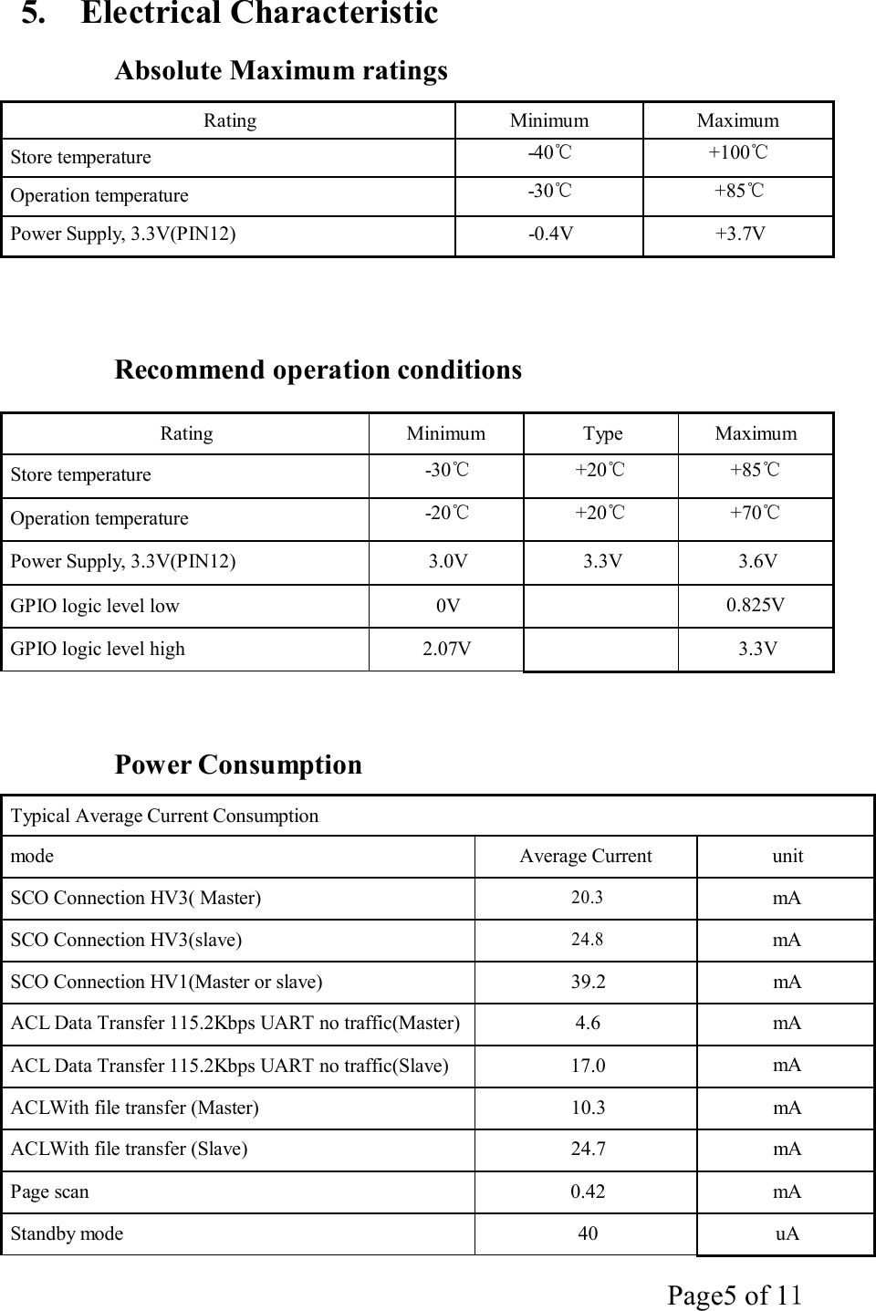
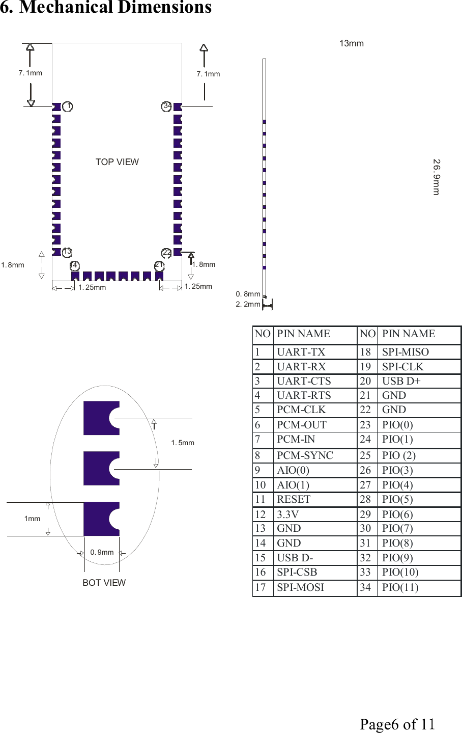
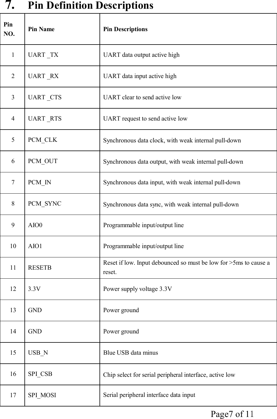
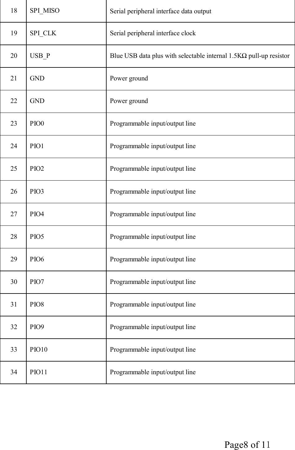
Xiamen PRT Technology SCBM4A Bluetooth Module User Manual

Xiamen PRT Technology Co., Ltd Bluetooth Module

User manual

Page1 of 11      The User Manual Of Bluetooth Module SCBM4A Rev. 3.1(April 2014)
Page2 of 11   Contents 1.  Device Features ........................................................................................................... 3 2.  Applications ................................................................................................................3 3.  General Description.................................................................................................... 3 4ˊ Key Features ................................................................................................................. 4 5.  Block Diagram ............................................................................................................4 6.  Electrical Characteristic ..............................................................................................5 Absolute Maximum ratings ............................................................................................ 5 Recommend operation conditions .................................................................................. 5 Power Consumption ....................................................................................................... 5 7.   Mechanical Dimensions ............................................................................................... 6 8.  Pin Definition Descriptions ......................................................................................... 7 9.  Reference Application Schematic ...............................................................................9 10. RF Test Report............................................................................................................ 10 11. Reference SMT Reflow Profile ................................................................................. 14 Reliability solder temperature chart ..............................................................................14 Reflow temperature chart .............................................................................................. 14
Page3 of 11   1.    Device Features    Bluetooth spec V2.1+EDR compliant   Enhanced data rate (EDR) compliant with V2.0.E.2 of specification for both 2Mbps and 3Mbps modulation modes    Class 2 type output power    Full Speed bluetooth operation with full piconet support    Scatternet support    Low power 3.3V operation    Minimum external components    USB, UART, SPI, PCM interface    Support for 8Mbit external flash onboard    Support for 802.11co-existence    RoHS compliant        2.    Applications     Bluetooth carkit    PCs    Personal digital assistants(PDAs)    Computer accessories(compact Flash Cards, PCMCIA Cards, SD Cards and USB Dongles)    Acess points    Digital cameras        3.    General Description  SCBM4A is a class 2 bluetooth module using BlueCore4 chipset from leading Bluetooth  chipset supplier cambridge silicon radio. SCBM4A  interfaces  up  to  8Mbit  of  16-bit  external  flash  memory.When  used  with  the  CSR  bluetooth software  stack,  it  provides  a  bluetooth  specification  V2.1+EDR  fully  compliant  system  for  data  and voice communications.
Page4 of 11   4.  Key Features    Operating frequency band  2.402GHz -2.480GHz  ISM band Bluetooth specification  V2.1+EDR Theoretical range in open field  Bluetooth class II Main chip  CSR BC417143 Transmitter power  +4dBm (Typical) Receive sensitivity  -82dB at 0.1% BER (Typical) Antenna  Interior Antenna impedance  50Ω Power supply  3.3V Flash memory size  8Mbit Audio interface  PCM and analog interface Dimension  26.9mm(L) * 13.0mm(W) * 2.2 mm(H)
Page5 of 11   5.  Electrical Characteristic  Absolute Maximum ratings  Rating  Minimum  Maximum Store temperature  -40℃  +100℃ Operation temperature  -30℃  +85℃ Power Supply, 3.3V(PIN12)  -0.4V  +3.7V      Recommend operation conditions  Rating  Minimum  Type  Maximum Store temperature  -30℃  +20℃  +85℃ Operation temperature  -20℃  +20℃  +70℃ Power Supply, 3.3V(PIN12)  3.0V  3.3V  3.6V GPIO logic level low  0V  0.825V GPIO logic level high  2.07V  3.3V     Power Consumption  Typical Average Current Consumption mode  Average Current  unit SCO Connection HV3( Master) 20.3 mA SCO Connection HV3(slave) 24.8 mA SCO Connection HV1(Master or slave)  39.2  mA ACL Data Transfer 115.2Kbps UART no traffic(Master) 4.6  mA ACL Data Transfer 115.2Kbps UART no traffic(Slave)  17.0  mA ACLWith file transfer (Master)  10.3  mA ACLWith file transfer (Slave)  24.7  mA Page scan  0.42  mA Standby mode  40  uA
Page6 of 11  NO PIN NAME NO PIN NAME 1 UART-TX 18 SPI-MISO 2 UART-RX 19 SPI-CLK 3 UART-CTS 20 USB D+ 4 UART-RTS 21 GND 5 PCM-CLK 22 GND 6 PCM-OUT 23 PIO(0) 7 PCM-IN 24 PIO(1) 8 PCM-SYNC 25 PIO (2) 9 AIO(0) 26 PIO(3) 10 AIO(1) 27 PIO(4) 11 RESET 28 PIO(5) 12 3.3V 29 PIO(6) 13 GND 30 PIO(7) 14 GND 31 PIO(8) 15 USB D- 32 PIO(9) 16 SPI-CSB 33 PIO(10) 17 SPI-MOSI 34 PIO(11)  26 . 9 m m  6. Mechanical Dimensions   13mm   7. 1mm 7. 1mm   1 34     TOP VIEW         13  22 1. 8mm  14   21  1. 8mm  1. 25mm 1. 25mm  0. 8mm 2. 2mm             1. 5mm       1mm   0. 9mm   BOT VIEW
Page7 of 11   7.  Pin Definition Descriptions   Pin NO.   Pin Name   Pin Descriptions  1  UART _TX  UART data output active high  2  UART _RX  UART data input active high  3  UART _CTS  UART clear to send active low  4  UART _RTS  UART request to send active low  5  PCM_CLK  Synchronous data clock, with weak internal pull-down  6  PCM_OUT  Synchronous data output, with weak internal pull-down  7  PCM_IN  Synchronous data input, with weak internal pull-down  8  PCM_SYNC  Synchronous data sync, with weak internal pull-down  9  AIO0  Programmable input/output line  10  AIO1  Programmable input/output line  11  RESETB  Reset if low. Input debounced so must be low for >5ms to cause a reset.  12  3.3V  Power supply voltage 3.3V  13  GND  Power ground  14  GND  Power ground  15  USB_N  Blue USB data minus  16  SPI_CSB  Chip select for serial peripheral interface, active low  17  SPI_MOSI  Serial peripheral interface data input
Page8 of 11    18  SPI_MISO  Serial peripheral interface data output  19  SPI_CLK  Serial peripheral interface clock  20  USB_P  Blue USB data plus with selectable internal 1.5KΩ pull-up resistor  21  GND  Power ground  22  GND  Power ground  23  PIO0  Programmable input/output line  24  PIO1  Programmable input/output line  25  PIO2  Programmable input/output line  26  PIO3  Programmable input/output line  27  PIO4  Programmable input/output line  28  PIO5  Programmable input/output line  29  PIO6  Programmable input/output line  30  PIO7  Programmable input/output line  31  PIO8  Programmable input/output line  32  PIO9  Programmable input/output line  33  PIO10  Programmable input/output line  34  PIO11  Programmable input/output line
Page9 of 11        D N G  2 G N D U SB_  D - SP I _ CS B SP I _ MO  SI SP I _ MISO SP I _ C L K U SB_  D + G N D   8.  Reference SMT Reflow Profile  Reliability solder temperature chart:          Reflow temperature chart
Page10 of 11
Page11 of 11    Warnings: This device complies with part 15 of the FCC Rules. Operation is subject to the following two conditions: (1) This device may not cause harmful interference, and (2) this device must accept any interference received, including interference that may cause undesired operation.  Any Changes or modifications not expressly approved by the party responsible for compliance could void the user's authority to operate the equipment.  Note: This equipment has been tested and found to comply with the limits for a Class B digital device, pursuant to part 15 of the FCC Rules. These limits are designed to provide reasonable protection against harmful interference in a residential installation. This equipment generates uses and can radiate radio frequency energy and, if not installed and used in accordance with the instructions, may cause harmful interference to radio communications. However, there is no guarantee that interference will not occur in a particular installation. If this equipment does cause harmful interference to radio or television reception, which can be determined by turning the equipment off and on, the user is encouraged to try to correct the interference by one or more of the following measures: -Reorient or relocate the receiving antenna. -Increase the separation between the equipment and receiver. -Connect the equipment into an outlet on a circuit different from that to which the receiver is connected. -Consult the dealer or an experienced radio/TV technician for help. FCC  Modular Radiation Exposure Statement: The antenna(s) used for this transmitter must be installed to provide a separation distance of at least 20 cm from all persons and must not be co-located or operating in conjunction with any other antenna or transmitter, except in accordance with FCC multi-transmitter product procedures. OEM and installers must be provided with antenna installation instructions and transmitter operating conditions for satisfying RF exposure compliance.
Page12 of 11  Single limited modular  statement: 1.This LMA does not have RF shielding and is tested and approved as standalone configuration, additional evaluation may be required for any system integrated this radio module. 2.The modular transmitter doesn’t have its own power supply regulation, it’s provided by host.    9.This module need to be soldered mounting in Printer main PCB according to module circuit diagram。  10. If the label of the module is not visible on the final device, the final device should contain the following text: "Contains FCC ID: Z5GSCBM4A”

Navigation menu