Xilinx Ml605 Users Manual UG534 Hardware, User Guide
ML605 to the manual 1170a4f4-6444-4052-a950-f66e3c686daf
2015-02-03
: Xilinx Xilinx-Ml605-Users-Manual-473575 xilinx-ml605-users-manual-473575 xilinx pdf
Open the PDF directly: View PDF ![]() .
.
Page Count: 92
- ML605 Hardware User Guide
- Table of Contents
- About This Guide
- ML605 Evaluation Board
- Overview
- Related Xilinx Documents
- Detailed Description
- 1. Virtex-6 XC6VLX240T-1FFG1156 FPGA
- 2. 512 MB DDR3 Memory SODIMM
- 3. 128 Mb Platform Flash XL
- 4. 32 MB Linear BPI Flash
- 5. System ACE CF and CompactFlash Connector
- 6. USB JTAG
- 7. Clock Generation
- 8. Multi-Gigabit Transceivers (GTX MGTs)
- 9. PCI Express Endpoint Connectivity
- 10. SFP Module Connector
- 11. 10/100/1000 Tri-Speed Ethernet PHY
- 12. USB-to-UART Bridge
- 13. USB Controller
- 14. DVI Codec
- 15. IIC Bus
- 16. Status LEDs
- 17. User I/O
- 18. Switches
- 19. VITA 57.1 FMC HPC Connector
- 20. VITA 57.1 FMC LPC Connector
- 21. Power Management
- 22. System Monitor
- Configuration Options
- Default Switch and Jumper Settings
- VITA 57.1 FMC LPC (J63) and HPC (J64) Connector Pinout
- ML605 Master UCF
- References

User Guide [optional]
UG534 (v1.2.1) January 21, 2010 [optional]
ML605 Hardware
User Guide
UG534 (v1.2.1) January 21, 2010
ML605 Hardware User Guide www.xilinx.com UG534 (v1.2.1) January 21, 2010
Xilinx is disclosing this user guide, manual, release note, and/or specification (the "Documentation") to you solely for use in the development
of designs to operate with Xilinx hardware devices. You may not reproduce, distribute, republish, download, display, post, or transmit the
Documentation in any form or by any means including, but not limited to, electronic, mechanical, photocopying, recording, or otherwise,
without the prior written consent of Xilinx. Xilinx expressly disclaims any liability arising out of your use of the Documentation. Xilinx reserves
the right, at its sole discretion, to change the Documentation without notice at any time. Xilinx assumes no obligation to correct any errors
contained in the Documentation, or to advise you of any corrections or updates. Xilinx expressly disclaims any liability in connection with
technical support or assistance that may be provided to you in connection with the Information.
THE DOCUMENTATION IS DISCLOSED TO YOU “AS-IS” WITH NO WARRANTY OF ANY KIND. XILINX MAKES NO OTHER
WARRANTIES, WHETHER EXPRESS, IMPLIED, OR STATUTORY, REGARDING THE DOCUMENTATION, INCLUDING ANY
WARRANTIES OF MERCHANTABILITY, FITNESS FOR A PARTICULAR PURPOSE, OR NONINFRINGEMENT OF THIRD-PARTY
RIGHTS. IN NO EVENT WILL XILINX BE LIABLE FOR ANY CONSEQUENTIAL, INDIRECT, EXEMPLARY, SPECIAL, OR INCIDENTAL
DAMAGES, INCLUDING ANY LOSS OF DATA OR LOST PROFITS, ARISING FROM YOUR USE OF THE DOCUMENTATION.
© 2009–2010 Xilinx, Inc. XILINX, the Xilinx logo, Virtex, Spartan, ISE, and other designated brands included herein are trademarks of Xilinx
in the United States and other countries. All other trademarks are the property of their respective owners. PCI, PCI Express, PCIe, and
PCI-X are trademarks of PCI-SIG.
Revision History
The following table shows the revision history for this document.
Date Version Revision
8/17/09 1.0 Initial Xilinx release.
11/17/09 1.1 •Updated Figure 1-1, Figure 1-2, Figure 1-3, Figure 1-11, and Figure 1-14.
•Added Figure 1-7, Figure 1-8, Figure 1-10, and Figure 1-13.
•Updated Table 1-15 and Table 1-18.
•Updated Appendix B, “VITA 57.1 FMC LPC (J63) and HPC (J64) Connector Pinout”
and Appendix C, “ML605 Master UCF.”
•Minor typographical edits.
01/15/10 1.2 •Updated Figure 1-2, Figure 1-3, Figure 1-17, Table 1-3, Table 1-8, Table 1-9, Table A-1,
and Table A-2. Miscellaneous typographical edits.
1/21/10 1.2.1 •Corrected typos in Table 1-31 and Figure 1-28.

ML605 Hardware User Guide www.xilinx.com 3
UG534 (v1.2.1) January 21, 2010
Preface: About This Guide
Guide Contents . . . . . . . . . . . . . . . . . . . . . . . . . . . . . . . . . . . . . . . . . . . . . . . . . . . . . . . . . . . . . . 5
Additional Documentation . . . . . . . . . . . . . . . . . . . . . . . . . . . . . . . . . . . . . . . . . . . . . . . . . . . 5
Additional Support Resources. . . . . . . . . . . . . . . . . . . . . . . . . . . . . . . . . . . . . . . . . . . . . . . . 6
Chapter 1: ML605 Evaluation Board
Overview . . . . . . . . . . . . . . . . . . . . . . . . . . . . . . . . . . . . . . . . . . . . . . . . . . . . . . . . . . . . . . . . . . . . 7
Additional Information . . . . . . . . . . . . . . . . . . . . . . . . . . . . . . . . . . . . . . . . . . . . . . . . . . . . . 7
Features . . . . . . . . . . . . . . . . . . . . . . . . . . . . . . . . . . . . . . . . . . . . . . . . . . . . . . . . . . . . . . . . . . 8
Block Diagram . . . . . . . . . . . . . . . . . . . . . . . . . . . . . . . . . . . . . . . . . . . . . . . . . . . . . . . . . . . 10
Related Xilinx Documents. . . . . . . . . . . . . . . . . . . . . . . . . . . . . . . . . . . . . . . . . . . . . . . . . . . 10
Detailed Description . . . . . . . . . . . . . . . . . . . . . . . . . . . . . . . . . . . . . . . . . . . . . . . . . . . . . . . . 11
1. Virtex-6 XC6VLX240T-1FFG1156 FPGA . . . . . . . . . . . . . . . . . . . . . . . . . . . . . . . . . . . . 13
Configuration . . . . . . . . . . . . . . . . . . . . . . . . . . . . . . . . . . . . . . . . . . . . . . . . . . . . . . . . . 13
I/O Voltage Rails . . . . . . . . . . . . . . . . . . . . . . . . . . . . . . . . . . . . . . . . . . . . . . . . . . . . . . 14
2. 512 MB DDR3 Memory SODIMM . . . . . . . . . . . . . . . . . . . . . . . . . . . . . . . . . . . . . . . . . 15
3. 128 Mb Platform Flash XL. . . . . . . . . . . . . . . . . . . . . . . . . . . . . . . . . . . . . . . . . . . . . . . . 20
4. 32 MB Linear BPI Flash . . . . . . . . . . . . . . . . . . . . . . . . . . . . . . . . . . . . . . . . . . . . . . . . . . 20
ML605 Flash Boot Options . . . . . . . . . . . . . . . . . . . . . . . . . . . . . . . . . . . . . . . . . . . . . . . 21
5. System ACE CF and CompactFlash Connector. . . . . . . . . . . . . . . . . . . . . . . . . . . . . . 24
6. USB JTAG . . . . . . . . . . . . . . . . . . . . . . . . . . . . . . . . . . . . . . . . . . . . . . . . . . . . . . . . . . . . . 26
7. Clock Generation . . . . . . . . . . . . . . . . . . . . . . . . . . . . . . . . . . . . . . . . . . . . . . . . . . . . . . . 27
Oscillator (Differential) . . . . . . . . . . . . . . . . . . . . . . . . . . . . . . . . . . . . . . . . . . . . . . . . . . 27
Oscillator Socket (Single-Ended, 2.5V) . . . . . . . . . . . . . . . . . . . . . . . . . . . . . . . . . . . . . . 27
SMA Connectors (Differential) . . . . . . . . . . . . . . . . . . . . . . . . . . . . . . . . . . . . . . . . . . . . 29
8. Multi-Gigabit Transceivers (GTX MGTs) . . . . . . . . . . . . . . . . . . . . . . . . . . . . . . . . . . . 31
9. PCI Express Endpoint Connectivity . . . . . . . . . . . . . . . . . . . . . . . . . . . . . . . . . . . . . . . 32
10. SFP Module Connector . . . . . . . . . . . . . . . . . . . . . . . . . . . . . . . . . . . . . . . . . . . . . . . . . 35
11. 10/100/1000 Tri-Speed Ethernet PHY . . . . . . . . . . . . . . . . . . . . . . . . . . . . . . . . . . . . 36
SGMII GTX Transceiver Clock Generation . . . . . . . . . . . . . . . . . . . . . . . . . . . . . . . . . . . 37
12. USB-to-UART Bridge. . . . . . . . . . . . . . . . . . . . . . . . . . . . . . . . . . . . . . . . . . . . . . . . . . . 39
13. USB Controller . . . . . . . . . . . . . . . . . . . . . . . . . . . . . . . . . . . . . . . . . . . . . . . . . . . . . . . . 40
14. DVI Codec . . . . . . . . . . . . . . . . . . . . . . . . . . . . . . . . . . . . . . . . . . . . . . . . . . . . . . . . . . . . 41
15. IIC Bus . . . . . . . . . . . . . . . . . . . . . . . . . . . . . . . . . . . . . . . . . . . . . . . . . . . . . . . . . . . . . . . 42
8 Kb NV Memory . . . . . . . . . . . . . . . . . . . . . . . . . . . . . . . . . . . . . . . . . . . . . . . . . . . . . . 44
16. Status LEDs . . . . . . . . . . . . . . . . . . . . . . . . . . . . . . . . . . . . . . . . . . . . . . . . . . . . . . . . . . . 45
Ethernet PHY Status LEDs . . . . . . . . . . . . . . . . . . . . . . . . . . . . . . . . . . . . . . . . . . . . . . . 46
FPGA INIT and DONE LEDs . . . . . . . . . . . . . . . . . . . . . . . . . . . . . . . . . . . . . . . . . . . . . 47
17. User I/O . . . . . . . . . . . . . . . . . . . . . . . . . . . . . . . . . . . . . . . . . . . . . . . . . . . . . . . . . . . . . 47
User LEDs . . . . . . . . . . . . . . . . . . . . . . . . . . . . . . . . . . . . . . . . . . . . . . . . . . . . . . . . . . . . 48
User Pushbutton Switches . . . . . . . . . . . . . . . . . . . . . . . . . . . . . . . . . . . . . . . . . . . . . . . 49
User DIP Switch . . . . . . . . . . . . . . . . . . . . . . . . . . . . . . . . . . . . . . . . . . . . . . . . . . . . . . . 50
User SMA GPIO . . . . . . . . . . . . . . . . . . . . . . . . . . . . . . . . . . . . . . . . . . . . . . . . . . . . . . . 51
LCD Display (16 Character x 2 Lines). . . . . . . . . . . . . . . . . . . . . . . . . . . . . . . . . . . . . . . 52
18. Switches . . . . . . . . . . . . . . . . . . . . . . . . . . . . . . . . . . . . . . . . . . . . . . . . . . . . . . . . . . . . . . 53
Power On/Off Slide Switch SW2 . . . . . . . . . . . . . . . . . . . . . . . . . . . . . . . . . . . . . . . . . . 53
Table of Contents

4www.xilinx.com ML605 Hardware User Guide
UG534 (v1.2.1) January 21, 2010
FPGA_PROG_B Pushbutton SW4 (Active-Low). . . . . . . . . . . . . . . . . . . . . . . . . . . . . . . 54
SYSACE_RESET_B Pushbutton SW3 (Active-Low) . . . . . . . . . . . . . . . . . . . . . . . . . . . . 54
System ACE CF CompactFlash Image Select DIP Switch S1. . . . . . . . . . . . . . . . . . . . . . 55
Mode, Osc Enable, Boot EEPROM Select, and Addr Select DIP Switch S2 . . . . . . . . . . . 56
19. VITA 57.1 FMC HPC Connector . . . . . . . . . . . . . . . . . . . . . . . . . . . . . . . . . . . . . . . . . 57
20. VITA 57.1 FMC LPC Connector . . . . . . . . . . . . . . . . . . . . . . . . . . . . . . . . . . . . . . . . . . 63
21. Power Management . . . . . . . . . . . . . . . . . . . . . . . . . . . . . . . . . . . . . . . . . . . . . . . . . . . . 65
AC Adapter and Input Power Jack/Switch . . . . . . . . . . . . . . . . . . . . . . . . . . . . . . . . . . 65
Onboard Power Regulation . . . . . . . . . . . . . . . . . . . . . . . . . . . . . . . . . . . . . . . . . . . . . . 66
22. System Monitor . . . . . . . . . . . . . . . . . . . . . . . . . . . . . . . . . . . . . . . . . . . . . . . . . . . . . . . 68
Configuration Options . . . . . . . . . . . . . . . . . . . . . . . . . . . . . . . . . . . . . . . . . . . . . . . . . . . . . . 73
Appendix A: Default Switch and Jumper Settings
Appendix B: VITA 57.1 FMC LPC (J63) and HPC (J64) Connector Pinout
Appendix C: ML605 Master UCF
Appendix D: References

ML605 Hardware User Guide www.xilinx.com 5
UG534 (v1.2.1) January 21, 2010
Preface
About This Guide
This manual accompanies the Virtex®-6 FPGA ML605 Evaluation Board and contains
information about the ML605 hardware and software tools.
Guide Contents
This manual contains the following chapters:
•Chapter 1, “ML605 Evaluation Board,” provides an overview of the embedded
development board and details the components and features of the ML605 board.
•Appendix A, “Default Switch and Jumper Settings.”
•Appendix B, “VITA 57.1 FMC LPC (J63) and HPC (J64) Connector Pinout.”
•Appendix C, “ML605 Master UCF.”
•Appendix D, “References.”
Additional Documentation
The following documents are also available for download at
http://www.xilinx.com/support/documentation/virtex-6.htm.
•Virtex-6 Family Overview
The features and product selection of the Virtex-6 family are outlined in this overview.
•Virtex-6 FPGA Data Sheet: DC and Switching Characteristics
This data sheet contains the DC and Switching Characteristic specifications for the
Virtex-6 family.
•Virtex-6 FPGA Packaging and Pinout Specifications
This specification includes the tables for device/package combinations and maximum
I/Os, pin definitions, pinout tables, pinout diagrams, mechanical drawings, and
thermal specifications.
•Virtex-6 FPGA Configuration Guide
This all-encompassing configuration guide includes chapters on configuration
interfaces (serial and SelectMAP), bitstream encryption, boundary-scan and JTAG
configuration, reconfiguration techniques, and readback through the SelectMAP and
JTAG interfaces.
•Virtex-6 FPGA Clocking Resources User Guide
This guide describes the clocking resources available in all Virtex-6 devices, including
the MMCM and PLLs.

6www.xilinx.com ML605 Hardware User Guide
UG534 (v1.2.1) January 21, 2010
Preface: About This Guide
•Virtex-6 FPGA Memory Resources User Guide
The functionality of the block RAM and FIFO are described in this user guide.
•Virtex-6 FPGA SelectIO Resources User Guide
This guide describes the SelectIO™ resources available in all Virtex-6 devices.
•Virtex-6 FPGA GTX Transceivers User Guide
This guide describes the GTX transceivers available in all Virtex-6 FPGAs except the
XC6VLX760.
•Virtex-6 FPGA Embedded Tri-Mode Ethernet MAC User Guide
This guide describes the dedicated Tri-Mode Ethernet Media Access Controller
available in all Virtex-6 FPGAs except the XC6VLX760.
•Virtex-6 FPGA DSP48E1 Slice User Guide
This guide describes the architecture of the DSP48E1 slice in Virtex-6 FPGAs and
provides configuration examples.
•Virtex-6 FPGA System Monitor User Guide
The System Monitor functionality available in all Virtex-6 devices is outlined in this
guide.
•Virtex-6 FPGA PCB Design Guide
This guide provides information on PCB design for Virtex-6 devices, with a focus on
strategies for making design decisions at the PCB and interface level.
Additional Support Resources
To search the database of silicon and software questions and answers or to create a
technical support case in WebCase, see the Xilinx website at:
http://www.xilinx.com/support.

ML605 Hardware User Guide www.xilinx.com 7
UG534 (v1.2.1) January 21, 2010
Chapter 1
ML605 Evaluation Board
Overview
The ML605 board enables hardware and software developers to create or evaluate designs
targeting the Virtex®-6 XC6VLX240T-1FFG1156 FPGA.
The ML605 provides board features common to many embedded processing systems.
Some commonly used features include: a DDR3 SODIMM memory, an 8-lane PCI
Express® interface, a tri-mode Ethernet PHY, general purpose I/O, and a UART.
Additional user desired features can be added through mezzanine cards attached to the
onboard high-speed VITA-57 FPGA Mezzanine Connector (FMC) high pin count (HPC)
expansion connector, or the onboard VITA-57 FMC low pin count (LPC) connector.
“Features,” page 8 provides a general listing of the board features with details provided in
“Detailed Description,” page 11.
Additional Information
Additional information and support material is located at:
•http://www.xilinx.com/ml605
This information includes:
•Current version of this user guide in PDF format
•Example design files for demonstration of Virtex-6 FPGA features and technology
•Demonstration hardware and software configuration files for the System ACE™ CF
controller, Platform Flash configuration storage device, and linear flash chip
•Reference design files
•Schematics in PDF and DxDesigner formats
•Bill of materials (BOM)
•Printed-circuit board (PCB) layout in Allegro PCB format
•Gerber files for the PCB (Many free or shareware Gerber file viewers are available on
the internet for viewing and printing these files.)
•Additional documentation, errata, frequently asked questions, and the latest news
For information about the Virtex-6 family of FPGA devices, including product highlights,
data sheets, user guides, and application notes, see the Virtex-6 FPGA documentation page
at http://www.xilinx.com/support/documentation/virtex-6.htm.

8www.xilinx.com ML605 Hardware User Guide
UG534 (v1.2.1) January 21, 2010
Chapter 1: ML605 Evaluation Board
Features
The ML605 provides the following features:
•1. Virtex-6 XC6VLX240T-1FFG1156 FPGA
•2. 512 MB DDR3 Memory SODIMM
•3. 128 Mb Platform Flash XL
•4. 32 MB Linear BPI Flash
•5. System ACE CF and CompactFlash Connector
•6. USB JTAG
•7. Clock Generation
♦Fixed 200 MHz oscillator (differential)
♦Socketed 2.5V oscillator (single-ended)
♦SMA connectors (differential)
♦SMA connectors for MGT clocking
•8. Multi-Gigabit Transceivers (GTX MGTs)
♦FMC - HPC connector
♦FMC - LPC connector
♦SMA
♦PCIe
♦SFP Module connector
♦Ethernet PHY SGMII interface
•9. PCI Express Endpoint Connectivity
♦Gen1 8-lane (x8)
♦Gen2 4-lane (x4)
•10. SFP Module Connector
•11. 10/100/1000 Tri-Speed Ethernet PHY
•12. USB-to-UART Bridge
•13. USB Controller
•14. DVI Codec
•15. IIC Bus
♦IIC EEPROM - 1 KB
♦DDR3 SODIMM socket
♦DVI CODEC
♦DVI connector
♦FMC HPC connector
♦FMC LPC connector
♦SFP module connector

ML605 Hardware User Guide www.xilinx.com 9
UG534 (v1.2.1) January 21, 2010
Overview
•16. Status LEDs
♦Ethernet status
♦FPGA INIT
♦FPGA DONE
♦System ACE CF Status
•17. User I/O
♦USER LED Group 1 - GPIO (8)
♦USER LED Group 2 - directional (5)
♦User pushbuttons - directional (5)
♦CPU reset pushbutton
♦User DIP switch - GPIO (8-pole)
♦User SMA GPIO connectors (2)
♦LCD character display (16 characters x 2 lines)
•18. Switches
♦Power on/off slide switch
♦System ACE CF reset pushbutton
♦System ACE CF bitstream image select DIP switch
♦Configuration MODE DIP switch
•19. VITA 57.1 FMC HPC Connector
•20. VITA 57.1 FMC LPC Connector
•21. Power Management
♦PMBus voltage and current monitoring via TI power controller
♦22. System Monitor
•Configuration Options
♦3. 128 Mb Platform Flash XL
♦4. 32 MB Linear BPI Flash
♦5. System ACE CF and CompactFlash Connector
♦6. USB JTAG
10 www.xilinx.com ML605 Hardware User Guide
UG534 (v1.2.1) January 21, 2010
Chapter 1: ML605 Evaluation Board
Block Diagram
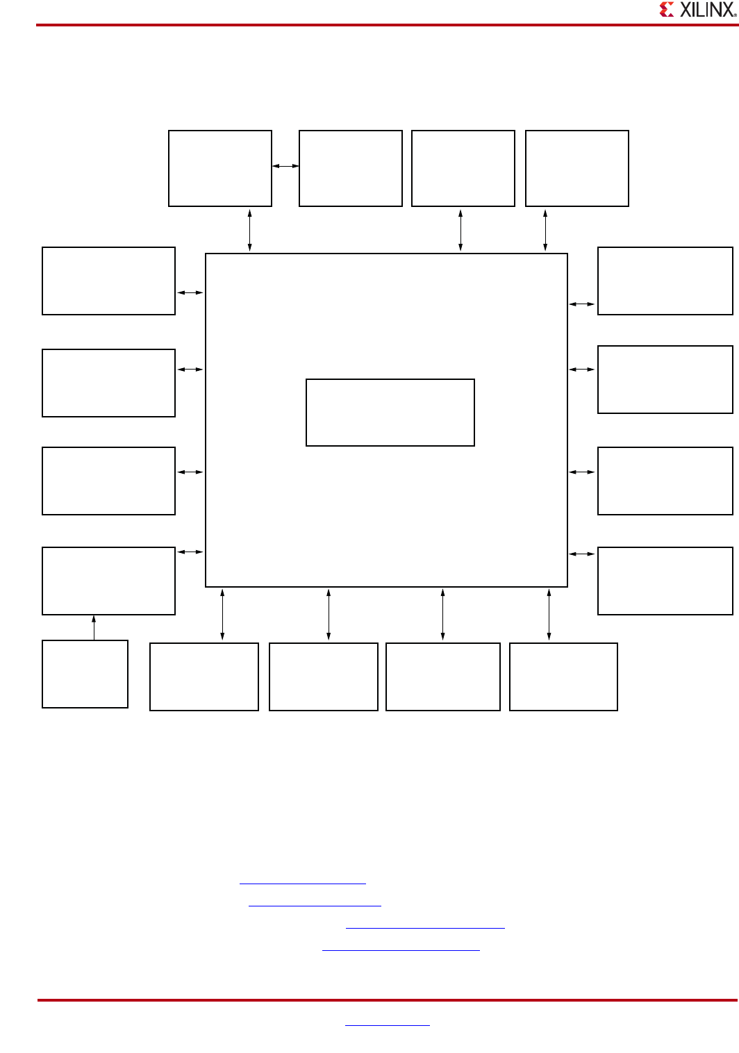
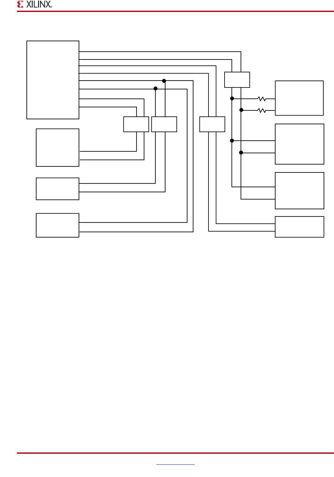
Figure 1-1 shows a high-level block diagram of the ML605 and its peripherals.
Related Xilinx Documents
Prior to using the ML605 Evaluation Board, users should be familiar with Xilinx resources.
See Appendix D, “References” for a direct link to Xilinx documentation. See the following
locations for additional documentation on Xilinx tools and solutions:
•ISE: www.xilinx.com/ise
•EDK: www.xilinx.com/edk
•Intellectual Property: www.xilinx.com/ipcenter
•Answer Browser: www.xilinx.com/support
X-Ref Target - Figure 1-1
Figure 1-1: ML605 High-Level Block Diagram
JTAG USB Mini-B
USB JTAG Circuit
VITA 57.1 FMC
HPC Connector
VITA 57.1 FMC
LPC Connector
Virtex-6
FPGA
XC6VLX240T - 1FFG1156
System ACE CF
S.A. CompactFlash
S.A. 8-bit MPU I/F
User LED/SW
User DIP SW
User LCD
200 MHz LVDS Clock
SMA Clock
User S.E. 2.5V Clock
USB Controller
Host Type “A”
Peripheral Mini-B
Connectors
CP2103 USB-TO-UART
Bridge
USB Mini-B
Platform Flash
Linear BPI Flash
DVI Codec
VGA Video
DVI Video Connector
10/100/1000
Ethernet PHY
MII/GMII/RMII
SYSMON I/F
INIT, DONE LEDs
PROG PB, MODE SW
IIC Bus
IIC EEPROM
FMC HPC
DDR3 SODIMM IIC
FMC LPC
SFP Module
Connector
SGMII
PCIe X8 Edge Connector
MGT SMA REF Clock
MGT RX/TX SMA Port
UG534_01_092709
SODIMM Socket
204-pin, DDR3
Decoupling Caps
MEM Vterm
Regulator
BANK32 BANK12, 13
BANK14,22
BANK23,24
BANK112,113
BANK24
BANK34
BANK32
BANK33 BANK116
BANK33
BANK34
BANK15,16
BANK34,116
BANK0
BANK24,34 BANK14
BANK114
BANK115
BANK24
BANK14, 33, 36
BANK 25, 35
BANK 26, 36
ML605 Hardware User Guide www.xilinx.com 11
UG534 (v1.2.1) January 21, 2010
Detailed Description
Detailed Description
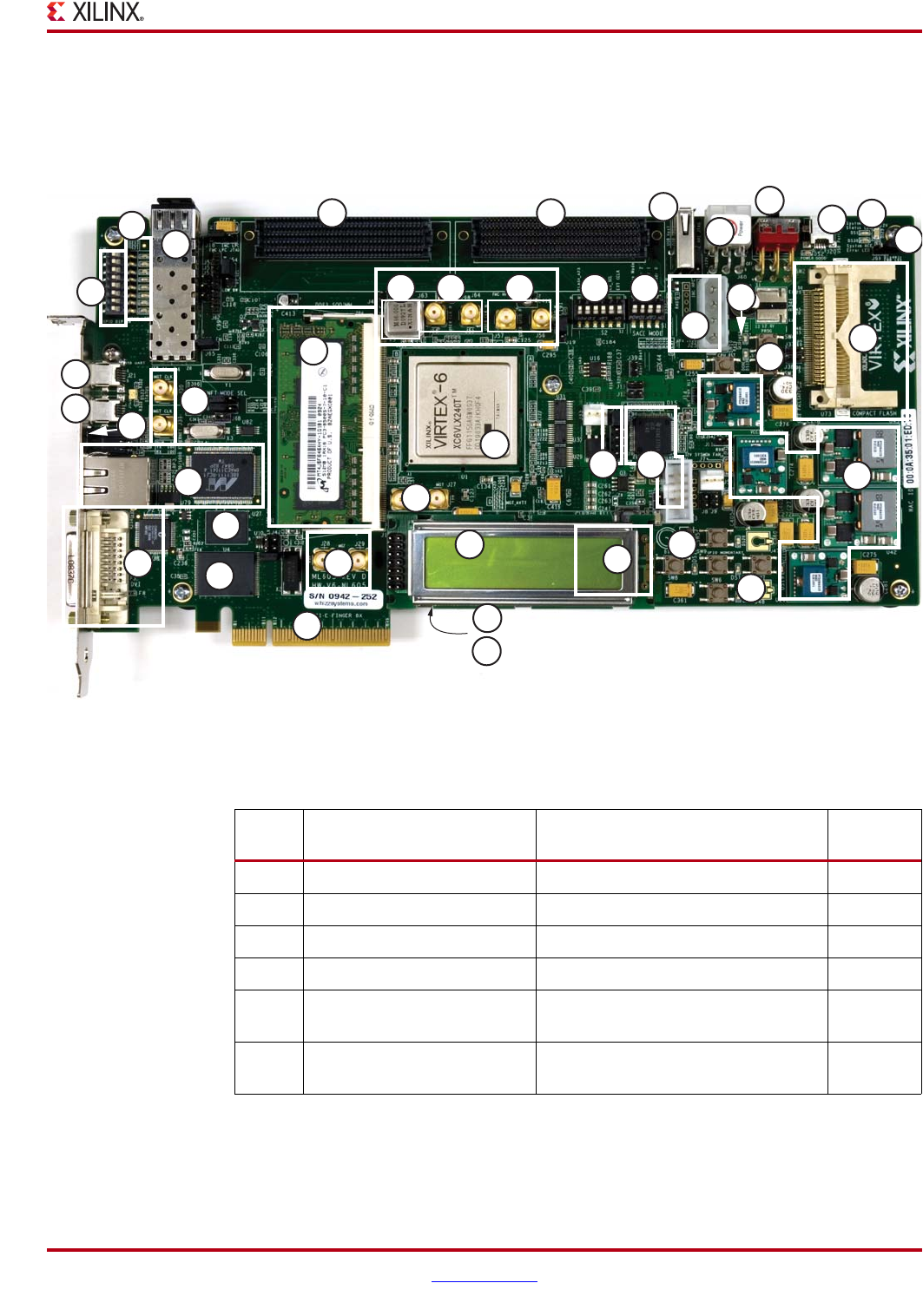
Figure 1-2 shows a board photo with numbered features corresponding to Table 1-1 and
the section headings in this document.
The numbered features in Figure 1-2 correlate to the features and notes listed in Table 1-1.
X-Ref Target - Figure 1-2
Figure 1-2: ML605 Board Photo
1
2
8
13
5
10
15
8
13
16b
16c
23
19 18a
18b
18c18d
7c 17e
17c
17b
17f 21a
21a21b
21c
21d
22
7a
(on backside)
7b
17a
17d
20
12
6
16a
7d
11
14
3
4
9
UG534_02_123009
Table 1-1: ML605 Features
Number Feature Notes Schematic
Page
1 Virtex-6 FPGA XC6VLX240T-1FFG1156 2 - 12
2 DDR3 SODIMM Micron 512 MB MT4JSF6464HY-1G1 15
3 128 Mb Platform Flash XL Xilinx XCF128X-FTG64C 25
4 Linear BPI Flash Numonyx JS28F256P30T95 26
5System ACE CF controller, CF
connector
Xilinx XCCACE-TQ144I
(bottom of board) 13
6JTAG cable connector (USB
Mini-B) USB JTAG download circuit 46
12 www.xilinx.com ML605 Hardware User Guide
UG534 (v1.2.1) January 21, 2010
Chapter 1: ML605 Evaluation Board
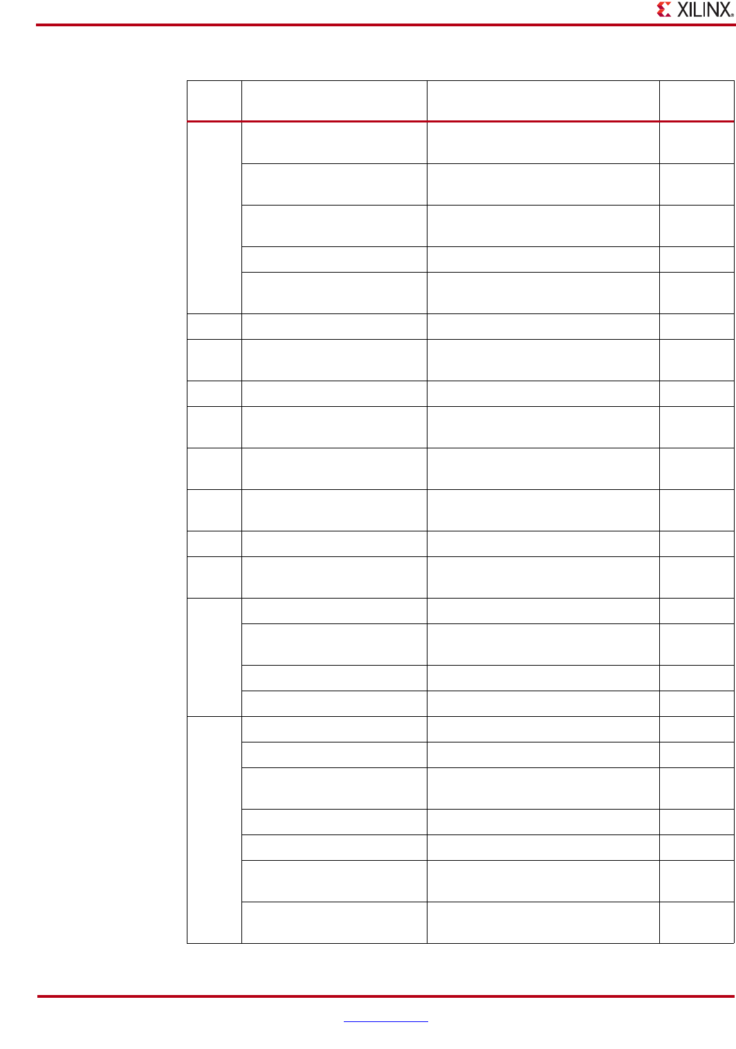
7
Clock generation 200 MHz OSC, oscillator socket, SMA
connectors 30
a. 200 MHz oscillator (on
backside) Epson 200 MHz 2.5V LVDS OSC 30
b. Oscillator socket, single-
ended MMD Components 66 MHz 2.5V 30
c. SMA connectors SMA pair 30
d. MGT REFCLK SMA
connectors SMA pair 30
8GTX RX/TX port SMA x4 30
9PCIe Gen1 (8-lane),
Gen2 (4-lane) Card edge connector, 8-lane 21
10 SFP connector and cage AMP 136073-1 23
11 Ethernet (10/100/1000) with
SGMII Marvell M88E1111 EPHY 24
12 USB Mini-B, USB-to-UART
bridge Silicon Labs CP2103GM bridge 33
13 USB-A Host, USB Mini-B
peripheral connectors
Cypress CY7C67300-100AXI
controller 27
14 Video - DVI connector Chrontel CH7301C-TF Video codec 28, 29
15 IIC NV EEPROM, 8 Kb
(on backside)
ST Microelectronics M24C08-
WDW6TP 32
16
Status LEDs 13, 24, 31
a. Ethernet status Right-angle link rate and direction
LEDs 24
b. FPGA INIT, DONE Init (red), Done (green) 31
c. System ACE CF status Status (green), Error (red) 13
17
User I/O 31
a. User LEDs, green (8) User I/O (active-High) 30, 31, 33
b. User pushbuttons, N.O.
momentary (5) User I/O (active-High) 31
c. User LEDs, green (5) User I/O (active-High) 31
d. User DIP switch (8-pole) User I/O (active-High) 31
e. User GPIO SMA
connectors SMA pair 30
f. LCD 16 character x 2 line
display Displaytech S162D BA BC 33
Table 1-1: ML605 Features (Cont’d)
Number Feature Notes Schematic
Page
ML605 Hardware User Guide www.xilinx.com 13
UG534 (v1.2.1) January 21, 2010
Detailed Description
1. Virtex-6 XC6VLX240T-1FFG1156 FPGA
A Virtex-6 XC6VLX240T-1FFG1156 FPGA is installed on the embedded development
board.
Keep-Out areas and drill holes are defined around the FPGA to support an Ironwood
Electronics SG-BGA-6046 FPGA socket.
References
See the Virtex-6 FPGA Data Sheet. [Ref 4]
Configuration
The ML605 supports configuration in the following modes:
•Slave SelectMAP (using Platform Flash XL with the onboard 47 MHz oscillator)
•Master BPI-Up (using Linear BPI Flash device)
•JTAG (using the included USB-A to Mini-B cable)
•JTAG (using System ACE CF and CompactFlash card)
18
Switches 13, 25, 39
a. Power On/Off Slide switch 39
b. FPGA_PROG_B
pushbutton active-Low 13
c. System ACE CF Image
Select 4-pole DIP switch (active-High) 25
d. Mode Switch 6-pole DIP switch (active-High) 25
19 FMC - HPC connector Samtec ASP-134486-01 16 -19
20 FMC - LPC connector Samtec ASP-134603-01 20
21
Power management 35 - 44
a. PMBus controllers 2 x TI UCD9240PFC 35, 40
b. Voltage regulators 2 x PTD08A020W, 3 x PTD08A010W 36-38, 43,
44
c. 12V power input
connector 6-pin Molex mini-fit connector 39
d. 12V power input
connector 4-pin ATX disk type connector 39
22 System Monitor Interface
connector 2x6 DIP male pin header 34
23 System ACE Error DS30 LED
disable jumper J69
Jumper on = enable LED
Jumper off = disable LED 13
Table 1-1: ML605 Features (Cont’d)
Number Feature Notes Schematic
Page
14 www.xilinx.com ML605 Hardware User Guide
UG534 (v1.2.1) January 21, 2010
Chapter 1: ML605 Evaluation Board
The ML605 supports Master BPI-Up, JTAG, and Slave SelectMAP. These are selected by
setting M[2:0] options 010, 101 and 110 shown in Table 1-2.
For an overview on configuring the FPGA, see “Configuration Options,” page 73.
Note: The mode switches are part of DIP switch S2. The default mode setting (see Ta bl e A -1 ,
page 75) is M[2:0]=010, which selects Master BPI-Up at board power-on. Switch S1 position 4 must
be OFF to disable the System ACE controller from attempting to boot if a CF card is present.
References
See the Virtex-6 FPGA Configuration User Guide for detailed configuration information.
[Ref 5]
I/O Voltage Rails
There are 16 I/O banks available on the Virtex-6 device. The voltage applied to the FPGA
I/O banks used by the ML605 board is summarized in Table 1-3.
Table 1-2: Virtex-6 FPGA Configuration Modes
Configuration Mode M[2:0] Bus Width(1) CCLK Direction
Master Serial(2) 000 1Output
Master SPI(2) 001 1Output
Master BPI-Up(2) 010 8, 16 Output
Master BPI-Down(2) 011 8, 16 Output
Master SelectMAP(2) 100 8, 16 Output
JTAG 101 1 Input (TCK)
Slave SelectMAP 110 8, 16, 32 Input
Slave Serial(3) 111 1 Input
Notes:
1. The parallel configuration modes bus is auto-detected by the configuration logic.
2. In Master configuration mode, the CCLK pin is the clock source for the Virtex-6 FPGA internal
configuration logic. The Virtex-6 FPGA CCLK output pin must be free from reflections to avoid
double-clocking the internal configuration logic. See the Virtex-6 FPGA Configuration User Guide for
more details. [Ref 5]
3. This is the default setting due to internal pull-up termination on mode pins.
Table 1-3: Voltage Rails
U1 FPGA Bank I/O Rail Voltage
Bank 0 VCC2V5_FPGA 2.5V
Bank 12(1) FMC_VIO_B_M2C 2.5V
Bank 13 VCC2V5_FPGA 2.5V
Bank 14 VCC2V5_FPGA 2.5V
Bank 15 VCC2V5_FPGA 2.5V
Bank 16 VCC2V5_FPGA 2.5V
Bank 22 VCC2V5_FPGA 2.5V
Bank 23 VCC2V5_FPGA 2.5V
ML605 Hardware User Guide www.xilinx.com 15
UG534 (v1.2.1) January 21, 2010
Detailed Description
References
See the Xilinx Virtex-6 FPGA documentation for more information at
http://www.xilinx.com/support/documentation/virtex-6.htm.
2. 512 MB DDR3 Memory SODIMM
A 512MB DDR3 SODIMM is provided as a flexible and efficient form-factor volatile
memory for user applications. The ML605 SODIMM socket is wired to support a
maximum SODIMM size of 2 GB.
The ML605 DDR3 64-bit wide interface has been tested to 800 MT/s.
The DDR3 interface is implemented in FPGA banks 25, 26, 35, and 36. DCI VRP/N resistor
connections are only implemented banks 26 and 36. DCI functionality in banks 25 and 35 is
achieved in the UCF by cascading DCI between adjacent banks as follows:
CONFIG DCI_CASCADE = "36 35";
CONFIG DCI_CASCADE = "26 25";
Table 1-4 shows the connections and pin numbers for the DDR3 SODIMM.
Bank 24 VCC2V5_FPGA 2.5V
Bank 25 VCC1V5_FPGA 1.5V
Bank 26 VCC1V5_FPGA 1.5V
Bank 32 VCC2V5_FPGA 2.5V
Bank 33 VCC2V5_FPGA 2.5V
Bank 34 VCC2V5_FPGA 2.5V
Bank 35 VCC1V5_FPGA 1.5V
Bank 36 VCC1V5_FPGA 1.5V
Notes:
1. The VITA 57.1 specification stipulates that the Bank 12 voltage named
FMC_VIO_B_M2C is supplied by the FMC card plugged onto the relevant
FMC connector (ML605 J64). FMC_VIO_B_M2C cannot exceed the base
board (ML605) Vadj of the FMC connector. The ML605 FMC Vadj
maximum is 2.5V.
Table 1-3: Voltage Rails (Cont’d)
U1 FPGA Bank I/O Rail Voltage
Table 1-4: DDR3 SODIMM Connections
U1 FPGA Pin Schematic Net Name
J1 SODIMM
Pin Number Pin Name
L14 DDR3_A0 98 A0
A16 DDR3_A1 97 A1
B16 DDR3_A2 96 A2
E16 DDR3_A3 95 A3
D16 DDR3_A4 92 A4
J17 DDR3_A5 91 A5

16 www.xilinx.com ML605 Hardware User Guide
UG534 (v1.2.1) January 21, 2010
Chapter 1: ML605 Evaluation Board
A15 DDR3_A6 90 A6
B15 DDR3_A7 86 A7
G15 DDR3_A8 89 A8
F15 DDR3_A9 85 A9
M16 DDR3_A10 107 A10/AP
M15 DDR3_A11 84 A11
H15 DDR3_A12 83 A12_BC_N
J15 DDR3_A13 119 A13
D15 DDR3_A14 80 A14
C15 DDR3_A15 78 A15
K19 DDR3_BA0 109 BA0
J19 DDR3_BA1 108 BA1
L15 DDR3_BA2 79 BA2
J11 DDR3_D0 5 DQ0
E13 DDR3_D1 7 DQ1
F13 DDR3_D2 15 DQ2
K11 DDR3_D3 17 DQ3
L11 DDR3_D4 4 DQ4
K13 DDR3_D5 6 DQ5
K12 DDR3_D6 16 DQ6
D11 DDR3_D7 18 DQ7
M13 DDR3_D8 21 DQ8
J14 DDR3_D9 23 DQ9
B13 DDR3_D10 33 DQ10
B12 DDR3_D11 35 DQ11
G10 DDR3_D12 22 DQ12
M11 DDR3_D13 24 DQ13
C12 DDR3_D14 34 DQ14
A11 DDR3_D15 36 DQ15
G11 DDR3_D16 39 DQ16
F11 DDR3_D17 41 DQ17
D14 DDR3_D18 51 DQ18
C14 DDR3_D19 53 DQ19
Table 1-4: DDR3 SODIMM Connections (Cont’d)
U1 FPGA Pin Schematic Net Name
J1 SODIMM
Pin Number Pin Name
ML605 Hardware User Guide www.xilinx.com 17
UG534 (v1.2.1) January 21, 2010
Detailed Description
G12 DDR3_D20 40 DQ20
G13 DDR3_D21 42 DQ21
F14 DDR3_D22 50 DQ22
H14 DDR3_D23 52 DQ23
C19 DDR3_D24 57 DQ24
G20 DDR3_D25 59 DQ25
E19 DDR3_D26 67 DQ26
F20 DDR3_D27 69 DQ27
A20 DDR3_D28 56 DQ28
A21 DDR3_D29 58 DQ29
E22 DDR3_D30 68 DQ30
E23 DDR3_D31 70 DQ31
G21 DDR3_D32 129 DQ32
B21 DDR3_D33 131 DQ33
A23 DDR3_D34 141 DQ34
A24 DDR3_D35 143 DQ35
C20 DDR3_D36 130 DQ36
D20 DDR3_D37 132 DQ37
J20 DDR3_D38 140 DQ38
G22 DDR3_D39 142 DQ39
D26 DDR3_D40 147 DQ40
F26 DDR3_D41 149 DQ41
B26 DDR3_D42 157 DQ42
E26 DDR3_D43 159 DQ43
C24 DDR3_D44 146 DQ44
D25 DDR3_D45 148 DQ45
D27 DDR3_D46 158 DQ46
C25 DDR3_D47 160 DQ47
C27 DDR3_D48 163 DQ48
B28 DDR3_D49 165 DQ49
D29 DDR3_D50 175 DQ50
B27 DDR3_D51 177 DQ51
G27 DDR3_D52 164 DQ52
A28 DDR3_D53 166 DQ53
Table 1-4: DDR3 SODIMM Connections (Cont’d)
U1 FPGA Pin Schematic Net Name
J1 SODIMM
Pin Number Pin Name
18 www.xilinx.com ML605 Hardware User Guide
UG534 (v1.2.1) January 21, 2010
Chapter 1: ML605 Evaluation Board
E24 DDR3_D54 174 DQ54
G25 DDR3_D55 176 DQ55
F28 DDR3_D56 181 DQ56
B31 DDR3_D57 183 DQ57
H29 DDR3_D58 191 DQ58
H28 DDR3_D59 193 DQ59
B30 DDR3_D60 180 DQ60
A30 DDR3_D61 182 DQ61
E29 DDR3_D62 192 DQ62
F29 DDR3_D63 194 DQ63
E11 DDR3_DM0 11 DM0
B11 DDR3_DM1 28 DM1
E14 DDR3_DM2 46 DM2
D19 DDR3_DM3 63 DM3
B22 DDR3_DM4 136 DM4
A26 DDR3_DM5 153 DM5
A29 DDR3_DM6 170 DM6
A31 DDR3_DM7 187 DM7
E12 DDR3_DQS0_N 10 DQS0_N
D12 DDR3_DQS0_P 12 DQS0_P
J12 DDR3_DQS1_N 27 DQS1_N
H12 DDR3_DQS1_P 29 DQS1_P
A14 DDR3_DQS2_N 45 DQS2_N
A13 DDR3_DQS2_P 47 DQS2_P
H20 DDR3_DQS3_N 62 DQS3_N
H19 DDR3_DQS3_P 64 DQS3_P
C23 DDR3_DQS4_N 135 DQS4_N
B23 DDR3_DQS4_P 137 DQS4_P
A25 DDR3_DQS5_N 152 DQS5_N
B25 DDR3_DQS5_P 154 DQS5_P
G28 DDR3_DQS6_N 169 DQS6_N
H27 DDR3_DQS6_P 171 DQS6_P
D30 DDR3_DQS7_N 186 DQS7_N
Table 1-4: DDR3 SODIMM Connections (Cont’d)
U1 FPGA Pin Schematic Net Name
J1 SODIMM
Pin Number Pin Name
ML605 Hardware User Guide www.xilinx.com 19
UG534 (v1.2.1) January 21, 2010
Detailed Description
The Memory Interface Generator (MIG) tool guidelines specify a set of U1 FPGA “No
Connect” pins. These should be added to the UCF as CONFIG PROHIBIT pins as follows:
CONFIG PROHIBIT = H22;
CONFIG PROHIBIT = F21;
CONFIG PROHIBIT = B20;
CONFIG PROHIBIT = F19;
CONFIG PROHIBIT = C13;
CONFIG PROHIBIT = M12;
CONFIG PROHIBIT = L13;
CONFIG PROHIBIT = K14;
CONFIG PROHIBIT = F25;
CONFIG PROHIBIT = C29;
CONFIG PROHIBIT = C28;
CONFIG PROHIBIT = D24;
References
See the Micron Technology, Inc. for more information [Ref 22].
In addition, see the Virtex-6 FPGA Memory Interface Solutions User Guide [Ref 6] and the
Virtex-6 FPGA Memory Resources User Guide [Ref 9].
C30 DDR3_DQS7_P 188 DQS7_P
F18 DDR3_ODT0 116 ODT0
E17 DDR3_ODT1 120 ODT1
E18 DDR3_RESET_B 30 RESET_B
K18 DDR3_S0_B 114 S0_B
K17 DDR3_S1_B 121 S1_B
D17 DDR3_TEMP_EVENT 198 EVENT_B
B17 DDR3_WE_B 113 WE_B
C17 DDR3_CAS_B 115 CAS_B
L19 DDR3_RAS_B 110 RAS_B
M18 DDR3_CKE0 73 CKE0
M17 DDR3_CKE1 74 CKE1
H18 DDR3_CLK0_N 103 CK0_N
G18 DDR3_CLK0_P 101 CK0_P
L16 DDR3_CLK1_N 104 CK1_N
K16 DDR3_CLK1_P 102 CK1_P
Table 1-4: DDR3 SODIMM Connections (Cont’d)
U1 FPGA Pin Schematic Net Name
J1 SODIMM
Pin Number Pin Name
20 www.xilinx.com ML605 Hardware User Guide
UG534 (v1.2.1) January 21, 2010
Chapter 1: ML605 Evaluation Board
3. 128 Mb Platform Flash XL
A 128 Mb Xilinx XCF128X-FTG64C Platform Flash XL device is used with an onboard
47 MHz oscillator (X4) to configure the FPGA in less than 100 ms from power valid as
required by the PCI Express Card Electromechanical Specification. This allows the PCIe
interface to be recognized and enumerated when plugged into a host PC.
To achieve the fastest configuration speed, the FPGA mode pins are set to Slave SelectMAP
and the onboard 47 MHz clock source external to the FPGA is used for configuration.
Configuration DIP switch S2, switch 1, controls the 47 MHz oscillator enable as outlined in
“18. Switches,” page 53.
See S2 switch setting details in Table 1-26, page 56. Also, see the “FPGA Design
Considerations for the Configuration Flash,” page 23 for FPGA design recommendations.
4. 32 MB Linear BPI Flash
A Numonyx JS28F256P30 Linear BPI Flash memory (P30) on the ML605 provides 32 MB of
non-volatile storage that can be used for configuration as well as software storage. The
Linear BPI Flash shares the dual use configuration pins in parallel with the XCF128
Platform Flash XL.
The P30_CS net is used to select the P30 or the XCF128. Power-on configuration is selected
by the P30_CS net which is tied to a dip switch S2 (selects pullup/pulldown) and is also
wired to an FPGA non-config pin. The dip switch allows power selection for the
configuration device P30 or XCF128XL. The dip switch selection can be overridden by the
FPGA after configuration by controlling the logic level of the P30_CS signal.
See S2 switch setting details in Table 1-26, page 56. For an overview on configuring the
FPGA, see “Configuration Options,” page 73.
Figure 1-3 shows a block diagram for the Platform Flash and BPI Flash.
X-Ref Target - Figure 1-3
Figure 1-3: Platform Flash and BPI Flash Block Diagram
UG534_03_011110
FPGA U1
Bank 34
FLASH_A[22:0]
FPGA U1
Bank 24
FLASH_A[23]
FLASH_D[15:0]
U4
U27
BPI
FLASH
PLATFORM
FLASH
AD
A
A23
D
CE
E
FPGA U1
Bank 24
U10
VCC2V5
VCC2V5
VCC2V5
PLATFLASH_FCS_B
FLASH_CE_B
FPGA_FCS_B FPGA U1
Bank 24
S2 SWITCH 2
ON = U4 BOOT
OFF = U27 BOOT
1
6
43
11
S2-2
2
VCC2V5
7
S2-6510
4.7K
510
4.7K
6
S2 SWITCH 6
ON = U4 BPI Upper Half
OFF = U4 BPI Lower Half P30_CS_SEL
(FPGA U1 pin AJ12)
S1 Switch 4
OFF = Disable System ACE,
enable U4/U27 flash boot
ON = Enable System ACE boot when
CF card is present
ML605 Hardware User Guide www.xilinx.com 21
UG534 (v1.2.1) January 21, 2010
Detailed Description
ML605 Flash Boot Options
The ML605 has two parallel wired flash memory devices as shown in Figure 1-3. At ML605
power-up, before FPGA configuration, DIP switch S2 switch 2 selects which flash device,
U4 (BPI) or U27 (Platform Flash), provides the boot bitstream. Typically S2 switch 2 will be
open/OFF to select the U27 Platform Flash. Given that the mode switches (S2 switch
3/M0, switch 4/M1 and switch 5/M2) are set to Slave SelectMAP mode, then U27, driven
at 47 MHz, can load a PCIe core bitstream before a host PC motherboard can scan its PCIe
slots.When S2 switch 2 is closed/ON at power up, the FPGA will be configured from the
BPI flash device U4. Note that U4 address bit A23 is switched by S2 switch 6, which allows
the lower or upper half of U4 to be chosen as a data source.
Table 1-5 shows the connections and pin numbers for the boot flash devices.
Table 1-5: Platform Flash and BPI Flash Connections
U1 FPGA Pin Schematic Net Name
U4 BPI Flash U27 Platform Flash
Pin Number Pin Name Pin Number Pin Name
AL8 FLASH_A0 29 A1 A1 A00
AK8 FLASH_A1 25 A2 B1 A01
AC9 FLASH_A2 24 A3 C1 A02
AD10 FLASH_A3 23 A4 D1 A03
C8 FLASH_A4 22 A5 D2 A04
B8 FLASH_A5 21 A6 A2 A05
E9 FLASH_A6 20 A7 C2 A06
E8 FLASH_A7 19 A8 A3 A07
A8 FLASH_A8 8 A9 B3 A08
A9 FLASH_A9 7 A10 C3 A09
D9 FLASH_A10 6 A11 D3 A10
C9 FLASH_A11 5 A12 C4 A11
D10 FLASH_A12 4 A13 A5 A12
C10 FLASH_A13 3 A14 B5 A13
F10 FLASH_A14 2 A15 C5 A14
F9 FLASH_A15 1 A16 D7 A15
AH8 FLASH_A16 55 A17 D8 A16
AG8 FLASH_A17 18 A18 A7 A17
AP9 FLASH_A18 17 A19 B7 A18
AN9 FLASH_A19 16 A20 C7 A19
AF10 FLASH_A20 11 A21 C8 A20
AF9 FLASH_A21 10 A22 A8 A21
AL9 FLASH_A22 9 A23 G1 A22
AA23 FLASH_A23 26 A24 NC A23

22 www.xilinx.com ML605 Hardware User Guide
UG534 (v1.2.1) January 21, 2010
Chapter 1: ML605 Evaluation Board
AF24 FLASH_D0 34 DQ0 F2 DQ00
AF25 FLASH_D1 36 DQ1 E2 DQ01
W24 FLASH_D2 39 DQ2 G3 DQ02
V24 FLASH_D3 41 DQ3 E4 DQ03
H24 FLASH_D4 47 DQ4 E5 DQ04
H25 FLASH_D5 49 DQ5 G5 DQ05
P24 FLASH_D6 51 DQ6 G6 DQ06
R24 FLASH_D7 53 DQ7 H7 DQ07
G23 FLASH_D8 35 DQ8 E1 DQ08
H23 FLASH_D9 37 DQ9 E3 DQ09
N24 FLASH_D10 40 DQ10 F3 DQ10
N23 FLASH_D11 42 DQ11 F4 DQ11
F23 FLASH_D12 48 DQ12 F5 DQ12
F24 FLASH_D13 50 DQ13 H5 DQ13
L24 FLASH_D14 52 DQ14 G7 DQ14
M23 FLASH_D15 54 DQ15 E7 DQ15
J26 FLASH_WAIT 56 WAIT NA(1) NA(1)
AF23 FPGA_FWE_B 14 /WE G8 /W
AA24 FPGA_FOE_B 32 /OE F8 /G
K8 FPGA_CCLK NA(1) NA(1) F1 K
AC23 PLATFLASH_L_B NA(1) NA(1) H1 /L
Y24 FPGA_FCS_B(2) NA(1) NA(1) NA(1) NA(1)
NA(1) PLATFLASH_FCS_B(3) NA(1) NA(1) B4 /E
NA(1) FLASH_CE_B(4) 30 /OE NA(1) NA(1)
Notes:
1. Not Applicable
2. FPGA control flash memory select signal connected to pin U10.3
3. Platform Flash select signal connected to pin U10.6
4. BPI Flash select signal connected to pin U10.4
Table 1-5: Platform Flash and BPI Flash Connections (Cont’d)
U1 FPGA Pin Schematic Net Name
U4 BPI Flash U27 Platform Flash
Pin Number Pin Name Pin Number Pin Name

ML605 Hardware User Guide www.xilinx.com 23
UG534 (v1.2.1) January 21, 2010
Detailed Description
FPGA Design Considerations for the Configuration Flash
After FPGA configuration, the FPGA design can disable the configuration flash or access
the configuration flash to read/write code or data.
When the FPGA design does not use the configuration flash, the FPGA design must drive
the FPGA FCS_B pin High in order to disable the configuration flash and put the flash into
a quiescent, low-power state. Otherwise, the Platform Flash XL, in particular, can continue
to drive its array data onto the data bus causing unnecessary switching noise and power
consumption.
For FPGA designs that access the flash for reading/writing stored code or data, connect
the FPGA design or EDK embedded memory controller (EMC) peripheral to the flash
through the pins defined in Table 1-5, page 21.
The Platform Flash XL defaults to a synchronous read mode. Typically, the Platform Flash
XL requires an initialization procedure to put the Platform Flash XL into the common,
asynchronous read mode before accessing stored code or data. To put the Platform Flash
XL into asynchronous read mode, apply the Set Configuration Register command
sequence. See the Platform Flash XL High-Density Configuration and Storage Device Data Sheet
for details on the Set Configuration Register command. [Ref 17]
References
See the Numonyx StrataFlash Embedded Memory Data Sheet. [Ref 24]
Visit the Xilinx Platform Flash product page and click the Resources tab for more
information.
Also, see the Platform Flash XL High-Density Configuration and Storage Device Data Sheet
[Ref 17] and the Virtex-6 Configuration User Guide [Ref 10].

24 www.xilinx.com ML605 Hardware User Guide
UG534 (v1.2.1) January 21, 2010
Chapter 1: ML605 Evaluation Board
5. System ACE CF and CompactFlash Connector
The Xilinx System ACE CompactFlash (CF) configuration controller allows a Type I or
Type II CompactFlash card to program the FPGA through the JTAG port. Both hardware
and software data can be downloaded through the JTAG port. The System ACE CF
controller supports up to eight configuration images on a single CompactFlash card. The
configuration address switches allow the user to choose which of the eight configuration
images to use.
The CompactFlash (CF) card shipped with the board is correctly formatted to enable the
System ACE CF controller to access the data stored in the card. The System ACE CF
controller requires a FAT16 file system, with only one reserved sector permitted, and a
sector-per-cluster size of more than one (UnitSize greater than 512). The FAT16 file system
supports partitions of up to 2 GB. If multiple partitions are used, the System ACE CF
directory structure must reside in the first partition on the CompactFlash, with the
xilinx.sys file located in the root directory. The xilinx.sys file is used by the System
ACE CF controller to define the project directory structure, which consists of one main
folder containing eight sub-folders used to store the eight ACE files containing the
configuration images. Only one ACE file should exist within each sub-folder. All folder
names must be compliant to the DOS 8.3 short file name format. This means that the folder
names can be up to eight characters long, and cannot contain the following reserved
characters: < > " / \ |. This DOS 8.3 file name restriction does not apply to the actual ACE
file names. Other folders and files may also coexist with the System ACE CF project within
the FAT16 partition. However, the root directory must not contain more than a total of 16
folder and/or file entries, including deleted entries. When ejecting or unplugging the
CompactFlash device, it is important to safely stop any read or write access to the
CompactFlash device to avoid data corruption.
System ACE CF error and status LEDs indicate the operational state of the System ACE CF
controller:
•A blinking red error LED indicates that no CompactFlash card is present.
•A solid red error LED indicates an error condition during configuration.
•A blinking green status LED indicates a configuration operation is ongoing.
•A solid green status LED indicates a successful download.
Note: Jumper J69 can be removed to disable the Red Error LED circuit. It is recommended that this
jumper is installed during operations utilizing the CompactFlash card.
Every time a CompactFlash card is inserted into the System ACE CF socket, a
configuration operation is initiated. Pressing the System ACE CF reset button re-programs
the FPGA.
Note: System ACE CF configuration is enabled by way of DIP switch S1. See “18. Switches,”
page 53 for more details.
The System ACE CF MPU port is connected to the FPGA. This connection allows the FPGA
to use the System ACE CF controller to reconfigure the system or access the CompactFlash
card as a generic FAT file system.
ML605 Hardware User Guide www.xilinx.com 25
UG534 (v1.2.1) January 21, 2010
Detailed Description
Table 1-6 lists the System ACE CF connections.
References
See the System ACE CF product page and the System ACE CompactFlash Solution Data Sheet.
[Ref 18]
Table 1-6: System ACE CF Connections
U1 FPGA Pin Schematic Net Name
U19 XCCACETQ144I
Pin Number Pin Name
AM15 SYSACE_D0 66 MPD00
AJ17 SYSACE_D1 65 MPD01
AJ16 SYSACE_D2 63 MPD02
AP16 SYSACE_D3 62 MPD03
AG16 SYSACE_D4 61 MPD04
AH15 SYSACE_D5 60 MPD05
AF16 SYSACE_D6 59 MPD06
AN15 SYSACE_D7 58 MPD07
AC15 SYSACE_MPA00 70 MPA00
AP15 SYSACE_MPA01 69 MPA01
AG17 SYSACE_MPA02 68 MPA02
AH17 SYSACE_MPA03 67 MPA03
AG15 SYSACE_MPA04 45 MPA04
AF15 SYSACE_MPA05 44 MPA05
AK14 SYSACE_MPA06 43 MPA06
AJ15 SYSACE_MPBRDY 39 MPBRDY
AJ14 SYSACE_MPCE 42 MPCE
L9 SYSACE_MPIRQ 41 MPIRQ
AL15 SYSACE_MPOE 77 MPOE
AL14 SYSACE_MPWE 76 MPWE
AC8 SYSACE_CFGTDI 81 CFGTDI
AE8 FPGA_TCK 80 CFGTCK
AD8 FPGA_TDI 82 CFGTDO
AF8 FPGA_TMS 85 CFGTMS
AE16 CLK_33MHZ_SYSACE(1) 93 CLK
Notes:
1. The System ACE CF clock is sourced from U28 32.000 MHz osc.
26 www.xilinx.com ML605 Hardware User Guide
UG534 (v1.2.1) January 21, 2010
Chapter 1: ML605 Evaluation Board
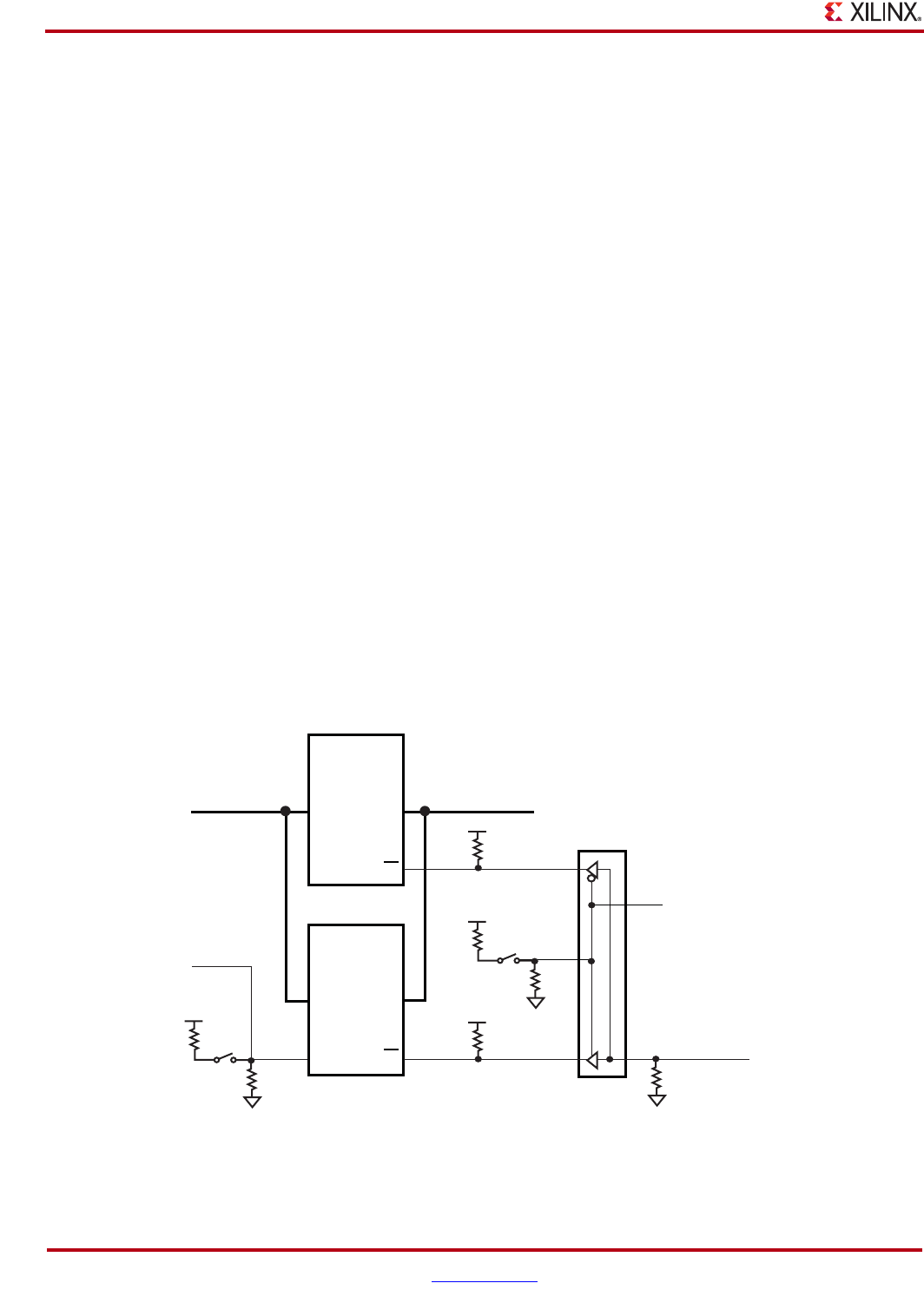
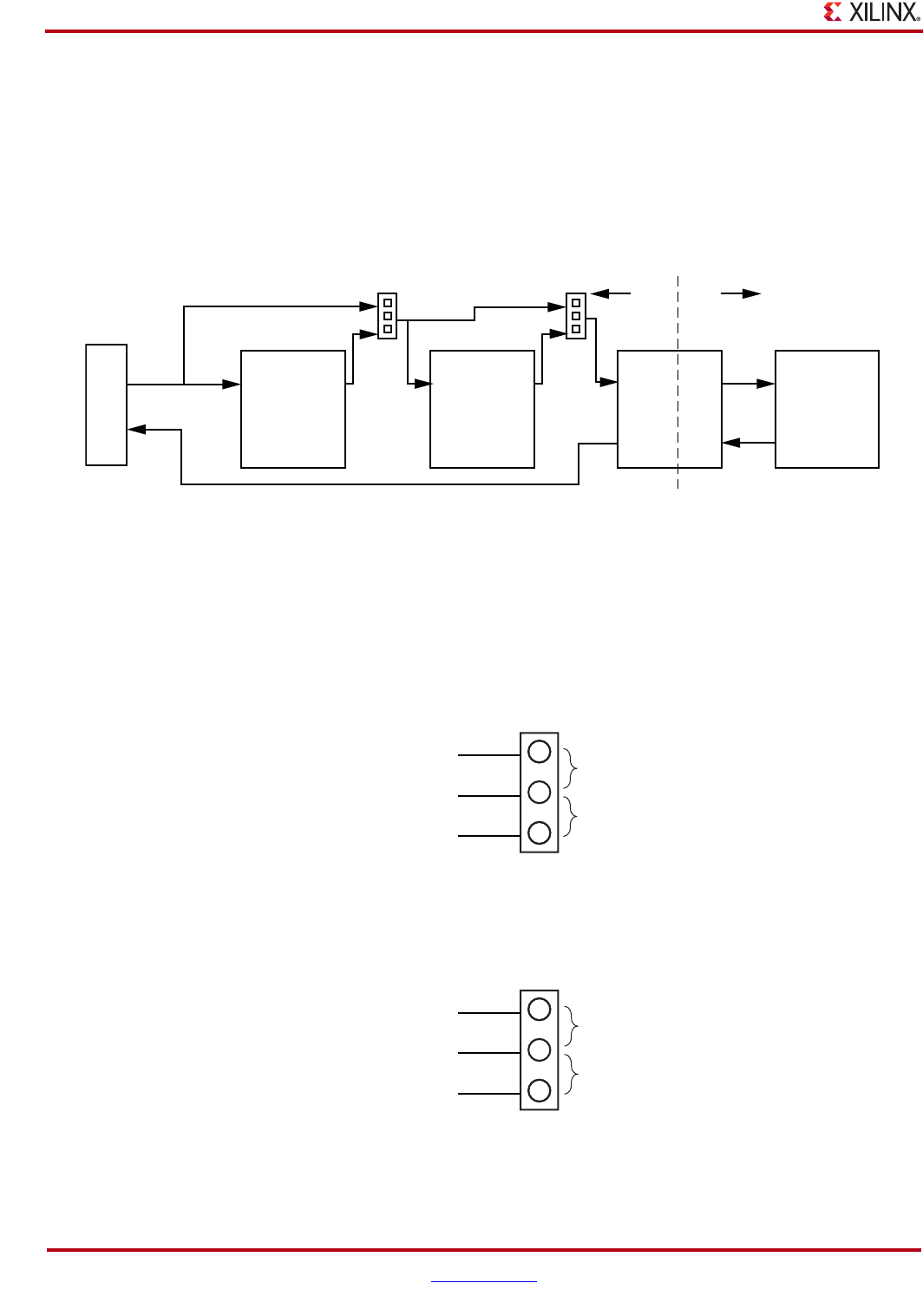
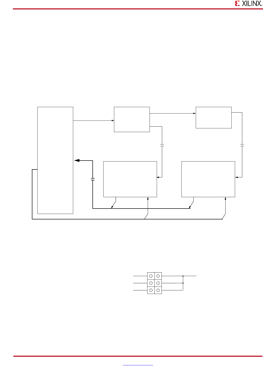
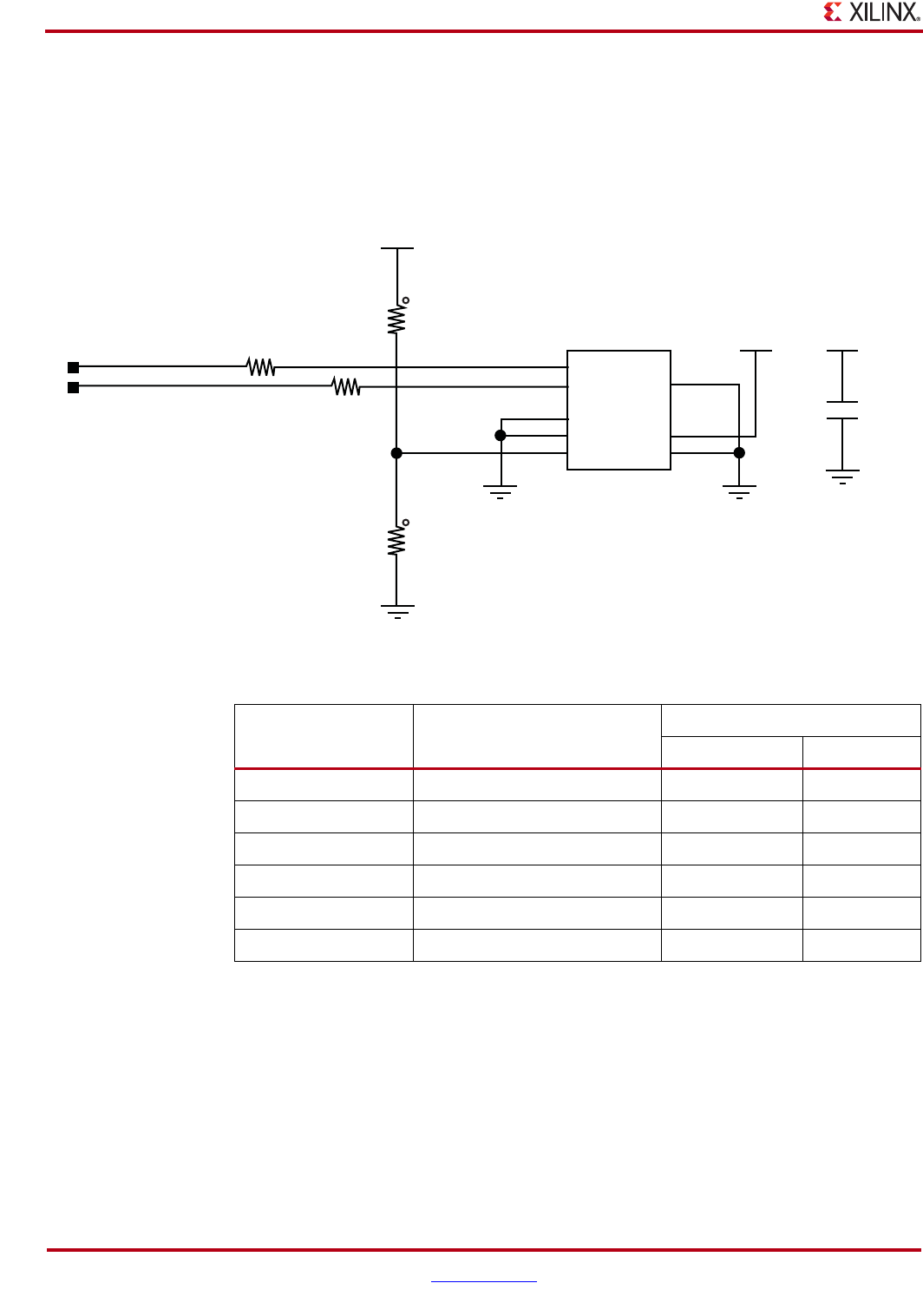
6. USB JTAG
JTAG configuration is provided through onboard USB-to-JTAG configuration logic where
a computer host accesses the ML605 JTAG chain through a Type-A (computer host side) to
Type-Mini-B (ML605 side) USB cable.
The JTAG chain of the board is illustrated in Figure 1-4. JTAG configuration is allowable at
any time under any mode pin setting. JTAG initiated configuration takes priority over the
mode pin settings.
FMC bypass jumpers J17 and J18 must be connected between pins 1-2 (bypass) to enable
JTAG access to the FPGA on the basic ML605 board (without FMC expansion modules
installed), as shown in Figure 1-5 and Figure 1-6. When either or both VITA 57.1 FMC
expansion connectors are populated with an expansion module that has a JTAG chain, the
respective jumper(s) must be set to connect pins 2-3 in order to include the FMC expansion
module's JTAG chain in the main ML605 JTAG chain.
X-Ref Target - Figure 1-4
Figure 1-4: JTAG Chain Diagram
J22
USB Mini-B
FMC HPC FMC LPC
TDI TDO
J64
TDI TDI
TDO
TDO
J63
J17 J18 3.3V 2.5V
System ACE CF FPGA
TSTTDI CFGTDO
TSTTDO CFGTDI
U19 U1
UG534_04_081309
X-Ref Target - Figure 1-5
Figure 1-5: VITA 57.1 FMC HPC (J64) JTAG Bypass Jumper J17
X-Ref Target - Figure 1-6
Figure 1-6: VITA 57.1 FMC LPC (J63) JTAG Bypass Jumper J18
J17
1
FMC_TDI_BUF Bypass FMC HPC J64 = Jumper 1-2
Include FMC HPC J64 = Jumper 2-3
H - 1x3
UG534_05_081309
2
FMC_LPC_TDI
3
FMC_HPC_TDO
J18
1
FMC_LPC_TDI Bypass FMC LPC J63 = Jumper 1-2
Include FMC LPC J63 = Jumper 2-3
H - 1x3
UG534_06_081309
2
SYSACE_TDI
3
FMC_LPC_TDO

ML605 Hardware User Guide www.xilinx.com 27
UG534 (v1.2.1) January 21, 2010
Detailed Description
The JTAG chain can be used to program the FPGA and access the FPGA for hardware and
software debug.
The JTAG connector (USB Mini-B J22) allows a host computer to download bitstreams to
the FPGA using the Xilinx iMPACT software tool. In addition, the JTAG connector allows
debug tools such as the ChipScope™ Pro Analyzer tool or a software debugger to access
the FPGA. The iMPACT software tool can also program the BPI flash via the USB J22
connection. iMPACT can download a temporary design to the FPGA through the JTAG.
This provides a connection within the FPGA from the FPGA's JTAG port to the FPGA's BPI
interface. Through the connection made by the temporary design in the FPGA, iMPACT
can indirectly program the BPI flash or the Platform Flash XL from the JTAG USB J22
connector.
For an overview on configuring the FPGA, see “Configuration Options,” page 73.
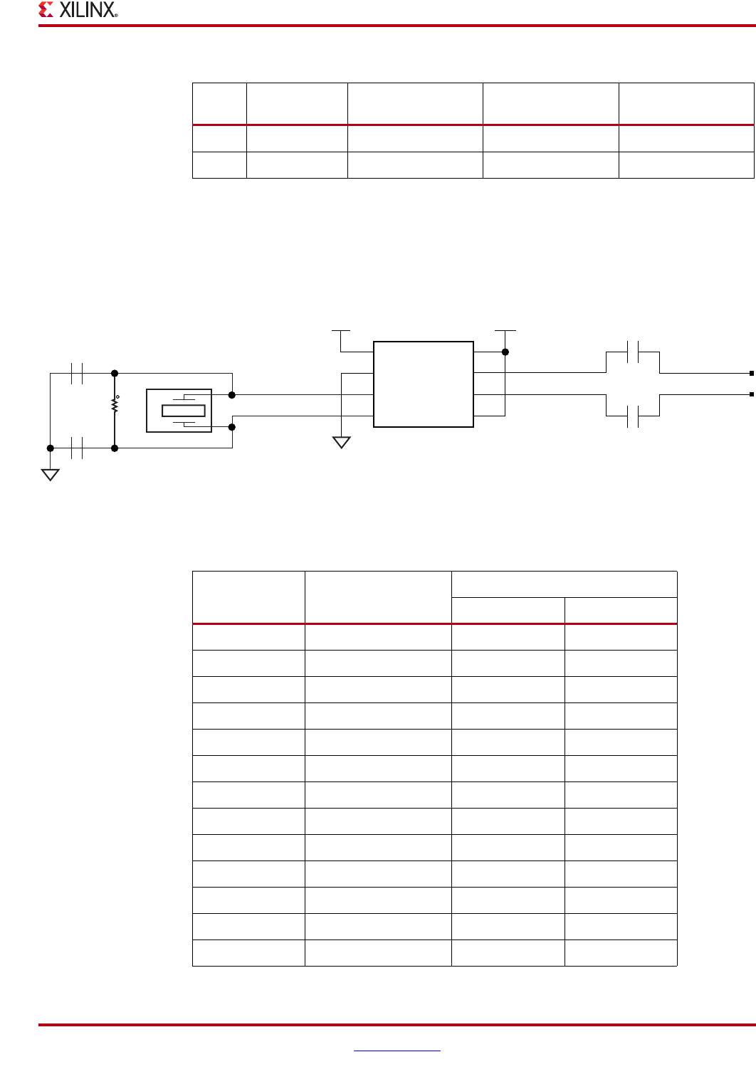
7. Clock Generation
There are three FPGA fabric clock sources available on the ML605.
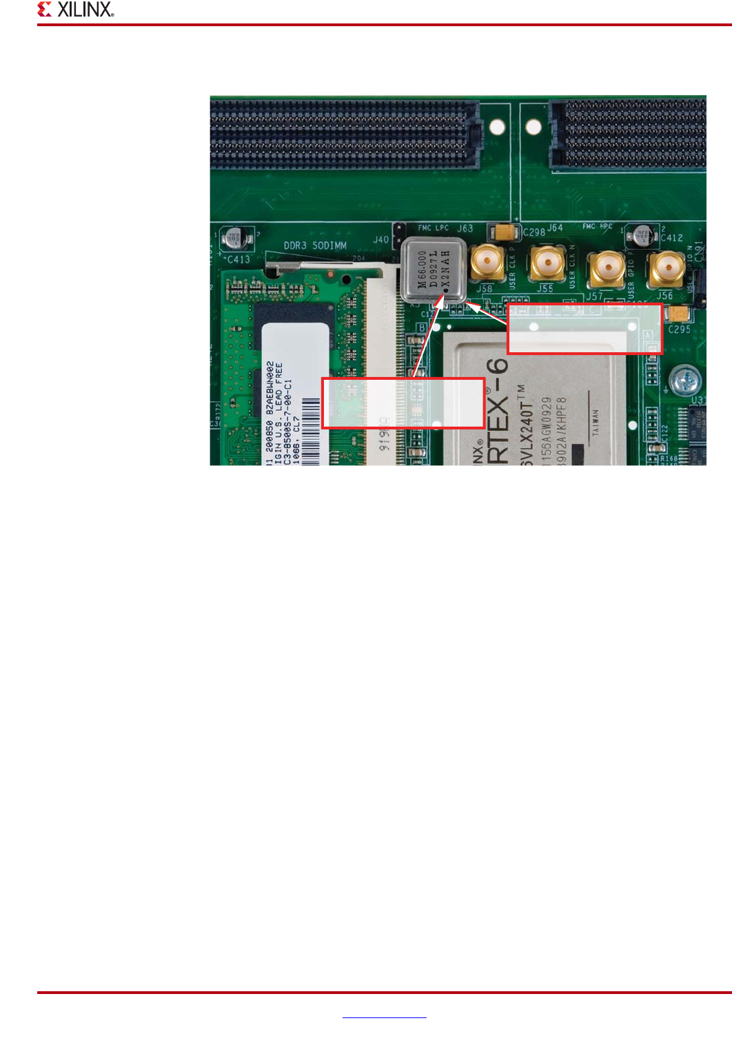
Oscillator (Differential)
The ML605 has one 2.5V LVDS differential 200 MHz oscillator (U11) soldered onto the
board and wired to an FPGA global clock input.
•Crystal oscillator: Epson EG-2121CA-200.0000M-LHPA
•PPM frequency jitter: 50 ppm
For more details, see the Epson EG-2121CA data sheet. [Ref 25].
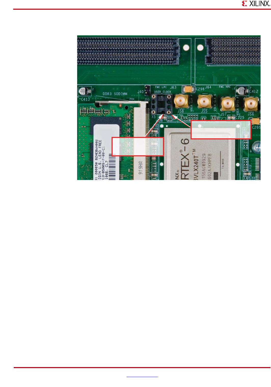
Oscillator Socket (Single-Ended, 2.5V)
One populated single-ended clock socket (X5) is provided for user applications. The option
of 3.3V or 2.5V power may be selected via a 0 ohm resistor selection. The X5 socket is
populated with a 66 MHz 2.5V single-ended MMD Components MBH2100H-66.000 MHz
oscillator.
For more details, see the MMD Components MBH Series Data Sheet. [Ref 26]
ML605 Hardware User Guide www.xilinx.com 29
UG534 (v1.2.1) January 21, 2010
Detailed Description
SMA Connectors (Differential)
A high-precision clock signal can be provided to the FPGA using differential clock signals
through the onboard 50-ohm SMA connectors J58(P)/J55(N).
X-Ref Target - Figure 1-8
Figure 1-8: ML605 Oscillator Pin 1 Location Identifiers
Oscillator top has
corner dot marking
UG534_08_092109
Oscillator body has
one square corner
30 www.xilinx.com ML605 Hardware User Guide
UG534 (v1.2.1) January 21, 2010
Chapter 1: ML605 Evaluation Board
GTX SMA Clock
The ML605 includes a pair of SMA connectors for a GTX (MGT) Clock as described in
Figure 1-9 and Table 1-7.
X-Ref Target - Figure 1-9
Figure 1-9: GTX SMA Clock
UG534_09_081309
SMA_REFCLK_C_N1
J30 32K10K-400E3
J31 32K10K-400E3
SMA_REFCLK_N
SMA_REFCLK_P
SMA_REFCLK_C_P1
GND1
GND2
GND3
GND4
SIG
SIG
GND5
GND6
GND7
GND1
GND2
GND3
GND4
GND5
GND6
GND7
2
3
4
5
6
7
8
2
3
4
5
6
7
8
C61 1
0.1UF
10V
X5R
2
C62 1
0.1UF
10V
X5R
2
Table 1-7: GTX SMA Clock Connections
U1 FPGA Pin Schematic Net Name SMA Pin
F5 SMA_REFCLK_N J30.1
F6 SMA_REFCLK_P J31.1
ML605 Hardware User Guide www.xilinx.com 31
UG534 (v1.2.1) January 21, 2010
Detailed Description
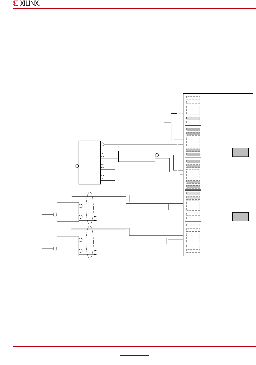
8. Multi-Gigabit Transceivers (GTX MGTs)
The ML605 provides access to 20 MGTs.
•Eight (8) of the MGTs are wired to the PCIe x8 Endpoint (P1) edge connector fingers
•Eight (8) of the MGTs are wired to the FMC HPC connector (J64)
•One (1) MGT is wired to SMA connectors (J26, J27)
•One (1) MGTs is wired to the FMC LPC connector (J63)
•One (1) MGT is wired to the SFP Module connector (P4)
•One (1) MGT is used for an SGMII connection to the Ethernet PHY (U80)
References
See the Virtex-6 FPGA GTX Transceivers User Guide. [Ref 12]
X-Ref Target - Figure 1-10
Figure 1-10: MGT Clocking
ICS
854104
100 MHz LVDS
100 MHz in from
No Connect
No Connect No Connect
PCIe Fingers
(HCSL)
250 MHz LVDS
GTX_X0Y19
GTX_X0Y18
GTX_X0Y17
GTX_X0Y16
GTX_X0Y15
GTX_X0Y14
GTX_X0Y13
GTX_X0Y12
GTX_X0Y11
GTX_X0Y10
GTX_X0Y09
GTX_X0Y08
GTX_X0Y07
GTX_X0Y06
GTX_X0Y05
GTX_X0Y04
GTX_X0Y03
GTX_X0Y02
GTX_X0Y01
GTX_X0Y00
PCIe
PCIe
BANK_115BANK_114BANK_113BANK_112 BANK_116
SGMII
SMA
SFP
FMC#2
PCIe Lane1
PCIe Lane 2
PCIe Lane 3
PCIe Lane 4
PCIe Lane 5
PCIe Lane 6
PCIe Lane 7
PCIe Lane 8
FMC#1
FMC#1
FMC#1
FMC#1
FMC#1
FMC#1
FMC#1
FMC#1
SMA xxx MHz LVDS
FMC#2 LPC xxxMHz GBTCLK0 LVDS
AC coupling on Mezz
SGMII 125 MHz LVDS
FMC#1 HPC xxx MHz LVDS GBTCLK0
REFCLK0
REFCLK1
REFCLK0
REFCLK1
REFCLK0
REFCLK1
REFCLK0
REFCLK1
REFCLK0
REFCLK1
AC coupling on Mezz
ICS
854104
(LVDS)
ICS
854104
(LVDS)
FMC#1 HPC CLK3_M2C
To FPGA CLK3_M2C_IO CC pin
FMC#1 HPC CLK2_M2C
To FPGA CLK2_M2C_IO CC pin
AC coupling on Mezz
FMC#1 HPC xxx MHz LVDS GBTCLK1
(LVDS)
(LVDS)
UG534_10_101409
Note: xxxMHz = user specified frequency
ICS874001
32 www.xilinx.com ML605 Hardware User Guide
UG534 (v1.2.1) January 21, 2010
Chapter 1: ML605 Evaluation Board
9. PCI Express Endpoint Connectivity
The 8-lane PCIe edge connector performs data transfers at the rate of 2.5 GT/s for a Gen1
application and 5.0 GT/s for a Gen2 application. The Virtex FPGA GTX MGTs are used for
the multi-gigabit per second serial interfaces.
The ML605 board trace impedance on all PCIe lanes supports both Gen1 and Gen2
applications. The ML605 supports up to Gen1 x8 and Gen2 x4 as shipped with a -1 speed
grade for the LX240T device.
Figure 1-11, page 32 is a diagram of the PCIe MGT bank 114 and 115 clocking.
PCIe lane width/size is selected via jumper J42 as shown in Figure 1-12. The default lane
size selection is 1-lane (J42 pins 1 and 2 jumpered).
X-Ref Target - Figure 1-11
Figure 1-11: PCIe MGT Banks 114 and 115 Clocking
UG534_11_100809
P1
U1
Bank 115
ICS874001
ICS854104
REFCLK+,-
PERp,n[7:0]
PCIE_TX[7:0]_P/N
PCIE_RX[7:0]_P/N
MGTREFCLK0 P/N
PETp,n[7:0]
PCIE_CLK_Q0_P/N
Note: PCIe edge connector signal nomenclature is
from perspective of the system/motherboard.
PCIE_100M_MGT1_P/N
PCIE_100M_MGT0_P/N
PCIE_100M_MGT0_C_P/N PCIE_250M_MGT1_C_P/N
PCIE_250M_MGT1_P/N
CLK/NCLK
PCIe
8-Lane
Edge
Connector
MGTTX
P/N[3:0]
MGTRX
P/N[3:0]
U1
Bank 114
MGTREFCLK0 P/N
MGTTX
P/N[7:4]
MGTRX
P/N[7:4]
U14
Q1/NQ1
Q0/NQ0
CLK/NCLK
U9
Q/NQ
X-Ref Target - Figure 1-12
Figure 1-12: PCIe Lane Size Select Jumper J42
J42
12
34
56
H-2X3
PCIE_PRSNT_B
PCIE_PRSNT_X8
PCIE_PRSNT_X4
PCIE_PRSNT_X1
UG534_12_111709
ML605 Hardware User Guide www.xilinx.com 33
UG534 (v1.2.1) January 21, 2010
Detailed Description
Table 1-8 shows the PCIe connector (P1) that provides up to 8-lane access through the GTX
transceivers to the Virtex-6 FPGA integrated Endpoint block for PCIe designs.
Table 1-8: PCIe Edge Connector Connections
U1 FPGA
Pin Schematic Net Name
P1 PCIe Edge Connector
Description Package
Placement
Pin Number Pin Name
F1 PCIE_TXO_P A16 PERp0 Integrated Endpoint block
transmit pair GTXE1_X0Y15
F2 PCIE_TXO_N A17 PERn0
H1 PCIE_TX1_P A21 PERp1 Integrated Endpoint block
transmit pair GTXE1_X0Y14
H2 PCIE_TX1_N A22 PERn1
K1 PCIE_TX2_P A25 PERp2 Integrated Endpoint block
transmit pair GTXE1_X0Y13
K2 PCIE_TX2_N A26 PERn2
M1 PCIE_TX3_P A29 PERp3 Integrated Endpoint block
transmit pair GTXE1_X0Y11
M2 PCIE_TX3_N A30 PERn3
P1 PCIE_TX4_P A35 PERp4 Integrated Endpoint block
transmit pair GTXE1_X0Y10
P2 PCIE_TX4_N A36 PERn4
T1 PCIE_TX5_P A39 PERp5 Integrated Endpoint block
transmit pair GTXE1_X0Y9
T2 PCIE_TX5_N A40 PERn5
V1 PCIE_TX6_P A43 PERp6 Integrated Endpoint block
transmit pair GTXE1_X0Y8
V2 PCIE_TX6_N A44 PERn6
Y1 PCIE_TX7_P A47 PERp7 Integrated Endpoint block
transmit pair GTXE1_X0Y7
Y2 PCIE_TX7_N A48 PERn7
J3 PCIE_RXO_P B14 PETp0 Integrated Endpoint block
receive pair GTXE1_X0Y15
J4 PCIE_RXO_N B15 PETn0
K5 PCIE_RX1_P B19 PETp1 Integrated Endpoint block
receive pair GTXE1_X0Y14
K6 PCIE_RX1_N B20 PETn1
L3 PCIE_RX2_P B23 PETp2 Integrated Endpoint block
receive pair GTXE1_X0Y13
L4 PCIE_RX2_N B24 PETn2
N3 PCIE_RX3_P B27 PETp3 Integrated Endpoint block
receive pair GTXE1_X0Y11
N4 PCIE_RX3_N B28 PETn3
R3 PCIE_RX4_P B33 PETp4 Integrated Endpoint block
receive pair GTXE1_X0Y10
R4 PCIE_RX4_N B34 PETn4
U3 PCIE_RX5_P B37 PETp5 Integrated Endpoint block
receive pair GTXE1_X0Y9
U4 PCIE_RX5_N B38 PETn5
W3 PCIE_RX6_P B41 PETp6 Integrated Endpoint block
receive pair GTXE1_X0Y8
W4 PCIE_RX6_N B42 PETn6
34 www.xilinx.com ML605 Hardware User Guide
UG534 (v1.2.1) January 21, 2010
Chapter 1: ML605 Evaluation Board
The PCIe interface obtains its power from the DC power supply provided with the ML605
or through the 12V ATX power supply connector. The PCIe edge connector is not used for
any power connections.
The board can be powered by one of two 12V sources; J60, a 6-pin (2x3) molex-type
connector and J25, a 4-pin (inline) ATX disk drive type connector.
The 6-pin molex-type connector provides 60W (12V @ 5A) from the AC power adapter
provided with the board while the 4-pin ATX disk drive connector is provided for users
who want to power their board while it is installed inside a PC chassis.
For applications requiring additional power, such as the use of expansion cards drawing
significant power, a larger AC adapter might be required. If a different AC adapter is used,
its load regulation should be better than ±10%.
ML605 power switch SW2 turns the board on and off by controlling the 12V supply to the
board.
Caution! Never apply power to the power brick connector (J60) and the 4-pin ATX disk drive
connector (J25) at the same time as this will result in damage to the board. See Figure 1-23,
page 53. Never connect an auxiliary PCIe 6-pin molex power connector to J60 6-pin molex on
the ML605 board as this could result in damage to the PCIe motherboard and/or ML605 board.
The 6-pin molex connector is marked with a no PCIe power label to warn users of the potential
hazard.
AA3 PCIE_RX7_P B45 PETp7 Integrated Endpoint block
receive pair GTXE1_X0Y7
AA4 PCIE_RX7_N B46 PETn7
P6 PCIE_100M_MGT0_P U14.16 Q0 Sourced from U14 ICS854104 GTXE1_X0Y6
P5 PCIE_100M_MGT0_N U14.15 NQ0 clock driver
V6 PCIE_250M_MGT1_P U9.18 Q Sourced from U9 ICS874001 GTXE1_X0Y4
V5 PCIE_250M_MGT1_N U9.17 NQ clock multiplier/driver
U14.6 PCIE_CLK_QO_P A13 REFCLK+ Integrated Endpoint block
differential clock pair from PCIe
edge connector
U14.7 PCIE_CLK_QO_N A14 REFCLK-
J42.2,4,6 PCIE_PRSNT_B A1 PRSNT#1 J42 Lane Size Select jumper
AD22 PCIE_WAKE_B B11 WAKE#
Integrated Endpoint block wake
signal, not connected on ML605
board
AE13 PCIE_PERST_B A11 PERST Integrated Endpoint block reset
signal
Notes:
1. PCIE_TXn_P/N pairs are capacitively coupled to FPGA
2. PCIE_100M_MGT0_P/N pairs are capacitively coupled to FPGA
3. PCIE_250M_MGT1_P/N pairs are capacitively coupled to FPGA
4. PCIE_PERST_B is level-shifted by U32
5. For ML605, access is through MGT Banks 114 and 115
Table 1-8: PCIe Edge Connector Connections (Cont’d)
U1 FPGA
Pin Schematic Net Name
P1 PCIe Edge Connector
Description Package
Placement
Pin Number Pin Name
ML605 Hardware User Guide www.xilinx.com 35
UG534 (v1.2.1) January 21, 2010
Detailed Description
References
See the following websites for more Virtex-6 FPGA Integrated Endpoint Block for PCI
Express information:
•http://www.xilinx.com/products/ipcenter/V6_PCI_Express_Block.htm
•http://www.xilinx.com/support/documentation/ipbusinterfacei-o_pci-
express_v6pciexpressendpointblock.htm
In addition, see the PCI Express specifications for more information. [Ref 27]
10. SFP Module Connector
The board contains a small form-factor pluggable (SFP) connector and cage assembly that
accepts SFP modules. The SFP interface is connected to MGT Bank 116 on the FPGA. The
SFP module serial ID interface is connected to the "SFP" IIC bus (see “15. IIC Bus,” page 42
for more information). The control and status signals for the SFP module are connected to
jumpers and test points as described in Table 1-9. The SFP module connections are shown
in Table 1-10, page 36.
Table 1-9: SFP Module Control and Status
SFP Control/Status
Signal Board Connection
SFP_TX_FAULT
Test Point J52
High = Fault
Low = Normal Operation
SFP_TX_DISABLE
Jumper J65
Off = SFP Disabled
On = SFP Enabled
SFP_MOD_DETECT
Test Point J53
High = Module Not Present
Low = Module Present
SFP_RT_SEL
Jumper J54
Jumper Pins 1-2 = Full Bandwidth
Jumper Pins 2-3 = Reduced Bandwidth
SFP_LOS
Test Point J51
High = Loss of Receiver Signal
Low = Normal Operation
36 www.xilinx.com ML605 Hardware User Guide
UG534 (v1.2.1) January 21, 2010
Chapter 1: ML605 Evaluation Board
11. 10/100/1000 Tri-Speed Ethernet PHY
The ML605 utilizes the onboard Marvell Alaska PHY device (88E1111) for Ethernet
communications at 10, 100, or 1000 Mb/s. The board supports MII, GMII, RGMII, and
SGMII interfaces from the FPGA to the PHY (Table 1-11). The PHY connection to a user-
provided Ethernet cable is through a Halo HFJ11-1G01E RJ-45 connector with built-in
magnetics.
On power-up, or on reset, the PHY is configured to operate in GMII mode with PHY
address 0b00111 using the settings shown in Table 1-12. These settings can be overwritten
via software commands passed over the MDIO interface.
Table 1-10: SFP Module Connections
U1 FPGA Pin Schematic Net Name
P4 SFP Module Connector
Pin Number Pin Name
E3 SFP_RX_P 13 RDP_13
E4 SFP_RX_N 12 RDN_12
C3 SFP_TX_P 18 TDP_18
C4 SFP_TX_N 19 TDN_19
V23 SFP_LOS 8 LOS
AP12 SFP_TX_DISABLE(1) 3TX_DISABLE
Notes:
1. The SFP TX Disable pin 3 is driven by transistor Q22, the base of which is driven
by the FPGA signal SFP_TX_DISABLE_FPGA.
Table 1-11: PHY Default Interface Mode
Mode
Jumper Settings
J66 J67 J68
GMII/MII to copper
(default) Jumper over pins 1-2 Jumper over pins 1-2 No jumper
SGMII to copper,
no clock Jumper over pins 2-3 Jumper over pins 2-3 No jumper
RGMII Jumper over pins 1-2 No jumper Jumper on
Table 1-12: Board Connections for PHY Configuration Pins
Pin Connection on
Board
Bit[2]
Definition and Value
Bit[1]
Definition and Value
Bit[0]
Definition and Value
CFG0 VCC 2.5V PHYADR[2] = 1 PHYADR[1] = 1 PHYADR[0] = 1
CFG1 Ground ENA_PAUSE = 0 PHYADR[4] = 0 PHYADR[3] = 0
CFG2 VCC 2.5V ANEG[3] = 1 ANEG[2] = 1 ANEG[1] = 1
CFG3 VCC 2.5V ANEG[0] = 1 ENA_XC = 1 DIS_125 = 1
CFG4 VCC 2.5V HWCFG_MD[2] = 1 HWCFG_MD[1] = 1 HWCFG_MD[0] = 1
ML605 Hardware User Guide www.xilinx.com 37
UG534 (v1.2.1) January 21, 2010
Detailed Description
SGMII GTX Transceiver Clock Generation
An Integrated Circuit Systems ICS844021I chip generates a high-quality, low-jitter, 125-
MHz LVDS clock from an inexpensive 25-MHz crystal oscillator. This clock is sent to the
GTX driving the SGMII interface. Series AC coupling capacitors are also present to allow
the clock input of the FPGA to set the common mode voltage.
Table 1-13 shows the connections and pin numbers for the PHY.
CFG5 VCC 2.5V DIS_FC = 1 DIS_SLEEP = 1 HWCFG_MD[3] = 1
CFG6 PHY_LED_RX SEL_BDT = 0 INT_POL = 1 75/50 OHM = 0
Table 1-12: Board Connections for PHY Configuration Pins (Cont’d)
Pin Connection on
Board
Bit[2]
Definition and Value
Bit[1]
Definition and Value
Bit[0]
Definition and Value
X-Ref Target - Figure 1-13
Figure 1-13: Ethernet SGMII Clock - 125 MHz
VDDA_SGMIICLK
ICS84402II
VDDA VDD
VDD_SGMIICLK
SGMIICLK_QO_C_P SGMIICLK_QO_P
SGMIICLK_QO_N
SGMIICLK_QO_C_N
Q0
NQ0
OE
GND
XTAL_OUT
XTAL_IN
1
2
3
4
U82
125.00 MHz Clock
GND_SGMIICLK
SGMIICLK_XTAL_OUT
SGMIICLK_XTAL_IN
8
7
6
5
X3
25.000MHZ
R132
DNP
1%
1/16W
C55 1
0.1UF
10V 2
X5R
C347
33PF
50V
NPO
C56 1
0.1UF
10V 2
X5R
1
2
C348
33PF
50V
NPO
1
2
1
2
UG534_13_111709
Table 1-13: Ethernet PHYConnections
U1 FPGA Pin Schematic Net Name
U80 M88E1111
Pin Number Pin Name
AN14 PHY_MDIO 33 MDIO
AP14 PHY_MDC 35 MDC
AH14 PHY_INT 32 INT_B
AH13 PHY_RESET 36 RESET_B
AL13 PHY_CRS 115 CRS
AK13 PHY_COL 114 COL
AP11 PHY_RXCLK 7 RXCLK
AG12 PHY_RXER 8 RXER
AM13 PHY_RXCTL_RXDV 4 RXDV
AN13 PHY_RXD0 3 RXD0
AF14 PHY_RXD1 128 RXD1
AE14 PHY_RXD2 126 RXD2
AN12 PHY_RXD3 125 RXD3
38 www.xilinx.com ML605 Hardware User Guide
UG534 (v1.2.1) January 21, 2010
Chapter 1: ML605 Evaluation Board
References
See the Marvell Alaska Gigabit Ethernet Transceivers product page for more information.
[Ref 28]
Also, see the LogiCORE™ IP Tri-Mode Ethernet MAC User Guide. [Ref 19]
AM12 PHY_RXD4 124 RXD4
AD11 PHY_RXD5 123 RXD5
AC12 PHY_RXD6 121 RXD6
AC13 PHY_RXD7 120 RXD7
AH12 PHY_TXC_GTXCLK 14 GTXCLK
AD12 PHY_TXCLK 10 TXCLK
AH10 PHY_TXER 13 TXER
AJ10 PHY_TXCTL_TXEN 16 TXEN
AM11 PHY_TXD0 18 TXD0
AL11 PHY_TXD1 19 TXD1
AG10 PHY_TXD2 20 TXD2
AG11 PHY_TXD3 24 TXD3
AL10 PHY_TXD4 25 TXD4
AM10 PHY_TXD5 26 TXD5
AE11 PHY_TXD6 28 TXD6
AF11 PHY_TXD7 29 TXD7
A3 SGMII_TX_P 113 SIN_P
A4 SGMII_TX_N 112 SIN_N
B5 SGMII_RX_P 107 SOUT_P
B6 SGMII_RX_N 105 SOUT_N
Table 1-13: Ethernet PHYConnections (Cont’d)
U1 FPGA Pin Schematic Net Name
U80 M88E1111
Pin Number Pin Name
ML605 Hardware User Guide www.xilinx.com 39
UG534 (v1.2.1) January 21, 2010
Detailed Description
12. USB-to-UART Bridge
The ML605 contains a Silicon Labs CP2103GM USB-to-UART bridge device (U34) which
allows connection to a host computer with a USB cable. The USB cable is supplied in this
evaluation kit (Type A end to host computer, Type Mini-B end to ML605 connector J21).
Table 1-14 details the ML605 J21 pinout.
Xilinx UART IP is expected to be implemented in the FPGA fabric (for instance, Xilinx XPS
UART Lite. The FPGA supports the USB-to-UART bridge using four signal pins: Transmit
(TX), Receive (RX), Request to Send (RTS), and Clear to Send (CTS).
Silicon Labs provides royalty-free Virtual COM Port (VCP) drivers which permit the
CP2103GM USB-to-UART bridge to appear as a COM port to host computer
communications application software (for example, HyperTerm or TeraTerm). The VCP
device driver must be installed on the host PC prior to establishing communications with
the ML605. Refer to the evaluation kit Getting Started Guide for driver installation
instructions.
References
Refer to the Silicon Labs website for technical information on the CP2103GM and the VCP
drivers.
In addition, see some of the Xilinx UART IP specifications at:
•http://www.xilinx.com/support/documentation/ip_documentation/xps_uartlite.pdf
•http:
//
www.xilinx.com/support/documentation/ip_documentation/xps_uart16550.pdf
Table 1-14: USB Type B Pin Assignments and Signal Definitions
USB Connector
Pin Signal Name Description
1 VBUS +5V from host system (not used)
2 USB_DATA_N Bidirectional differential serial data (N-side)
3 USB_DATA_P Bidirectional differential serial data (P-side)
4 GROUND Signal ground
Table 1-15: USB-to-UART Connections
U1 FPGA Pin UART function
in FPGA
Schematic Net
Name
U34 CP2103GM
Pin
UART Function
in CP2103GM
T24 RTS, output USB_1_CTS 22 CTS, input
T23 CTS, input USB_1_RTS 23 RTS, output
J25 TX, data out USB_1_RX 24 RXD, data in
J24 RX, data in USB_1_TX 25 TXD, data out
40 www.xilinx.com ML605 Hardware User Guide
UG534 (v1.2.1) January 21, 2010
Chapter 1: ML605 Evaluation Board
13. USB Controller
The ML605 provides USB support via a Cypress CY7C67300 EZ-Host™ Programmable
Embedded USB Host and Peripheral Controller (U81). The host port is a USB Type-A
connector (J5). A USB keyboard (without an internal USB hub) will be able to connect to
this USB Host port to demonstrate functionality. The peripheral port is a USB Type Mini-
B (J20).
References
See the Cypress CY7C67300 Data Sheet for more information. [Ref 29]
In addition, see the USB Specifications for more information. [Ref 30]
The FPGA requires implementation of a peripheral controller in order to communicate
with the Cypress USB device. See the XPS External Peripheral Controller (EPC) v1.02a Data
Sheet for more information. [Ref 20]
Table 1-16: USB Controller Connections
U1 FPGA
Pin Schematic Net Name
U81 USB Controller
Pin
Number Pin Name
Y32 USB_A0_LS 52 GPIO19_A0_CS0_52
W26 USB_A1_LS 50 50_GPIO20_A1_CS1
W27 USB_CS_B_LS 49 49_GPIO21_CS_N
R33 USB_D0_LS 94 GPIO0_D0_94
R34 USB_D1_LS 93 GPIO1_D1_93
T30 USB_D2_LS 92 GPIO2_D2_92
T31 USB_D3_LS 91 GPIO3_D3_91
T29 USB_D4_LS 90 GPIO4_D4_90
V28 USB_D5_LS 89 GPIO5_D5_89
V27 USB_D6_LS 87 GPIO6_D6_87
U25 USB_D7_LS 86 GPIO7_D7_86
Y28 USB_D8_LS 66 GPIO8_D8_MISO_66
W32 USB_D9_LS 65 GPIO9_D9_nSSI_65
W31 USB_D10_LS 61 GPIO10_D10_SCK_61
Y29 USB_D11_LS 60 GPIO11_D11_MOSI_60
W29 USB_D12_LS 59 GPIO12_D12_59
Y34 USB_D13_LS 58 GPIO13_D13_58
Y33 USB_D14_LS 57 GPIO14_D14_57
Y31 USB_D15_LS 56 GPIO15_D15_SSI_N_56
Y27 USB_INT_LS 46 46_GPIO24_INT_IORDY_IRQ0
W25 USB_RD_B_LS 47 47_GPIO23_RD_N_IOR
T25 USB_RESET_B_LS 85 RESET_N_85
V25 USB_WR_B_LS 48 48_GPIO22_WR_N_IOW
ML605 Hardware User Guide www.xilinx.com 41
UG534 (v1.2.1) January 21, 2010
Detailed Description
14. DVI Codec
The ML605 features a DVI connector (P3) to support an external video monitor. The DVI
circuitry utilizes a Chrontel CH7301C (U38) capable of 1600 X 1200 resolution with 24-bit
color. The video interface chip drives both the digital and analog signals to the DVI
connector. A DVI monitor can be connected to the board directly. A VGA monitor can also
be connected to the board using the supplied DVI-to-VGA adaptor. The Chrontel
CH7301C is controlled by way of the video IIC bus.
The DVI connector (Table 1-17) supports the IIC protocol to allow the board to read the
monitor's configuration parameters. These parameters can be read by the FPGA using the
DVI IIC bus (see “15. IIC Bus,” page 42).
Table 1-17: DVI Controller Connections
U1 FPGA Pin Schematic Net Name
U38 Chrontel CH7301C
Pin Number Pin Name
AJ19 DVI_D0 63 D0
AH19 DVI_D1 62 D1
AM17 DVI_D2 61 D2
AM16 DVI_D3 60 D3
AD17 DVI_D4 59 D4
AE17 DVI_D5 58 D5
AK18 DVI_D6 55 D6
AK17 DVI_D7 54 D7
AE18 DVI_D8 53 D8
AF18 DVI_D9 52 D9
AL16 DVI_D10 51 D10
AK16 DVI_D11 50 D11
AD16 DVI_DE 2 DE
AN17 DVI_H 4 H
AP17 DVI_RESET_B_LS 13 RESET_B
AD15 DVI_V 5 V
AC17 DVI_XCLK_N 56 XCLK_N
AC18 DVI_XCLK_P 57 XCLK_P
No Connect DVI_GPIO0 8 GPIO0
No Connect DVI_GPIO1 7 GPIO1

42 www.xilinx.com ML605 Hardware User Guide
UG534 (v1.2.1) January 21, 2010
Chapter 1: ML605 Evaluation Board
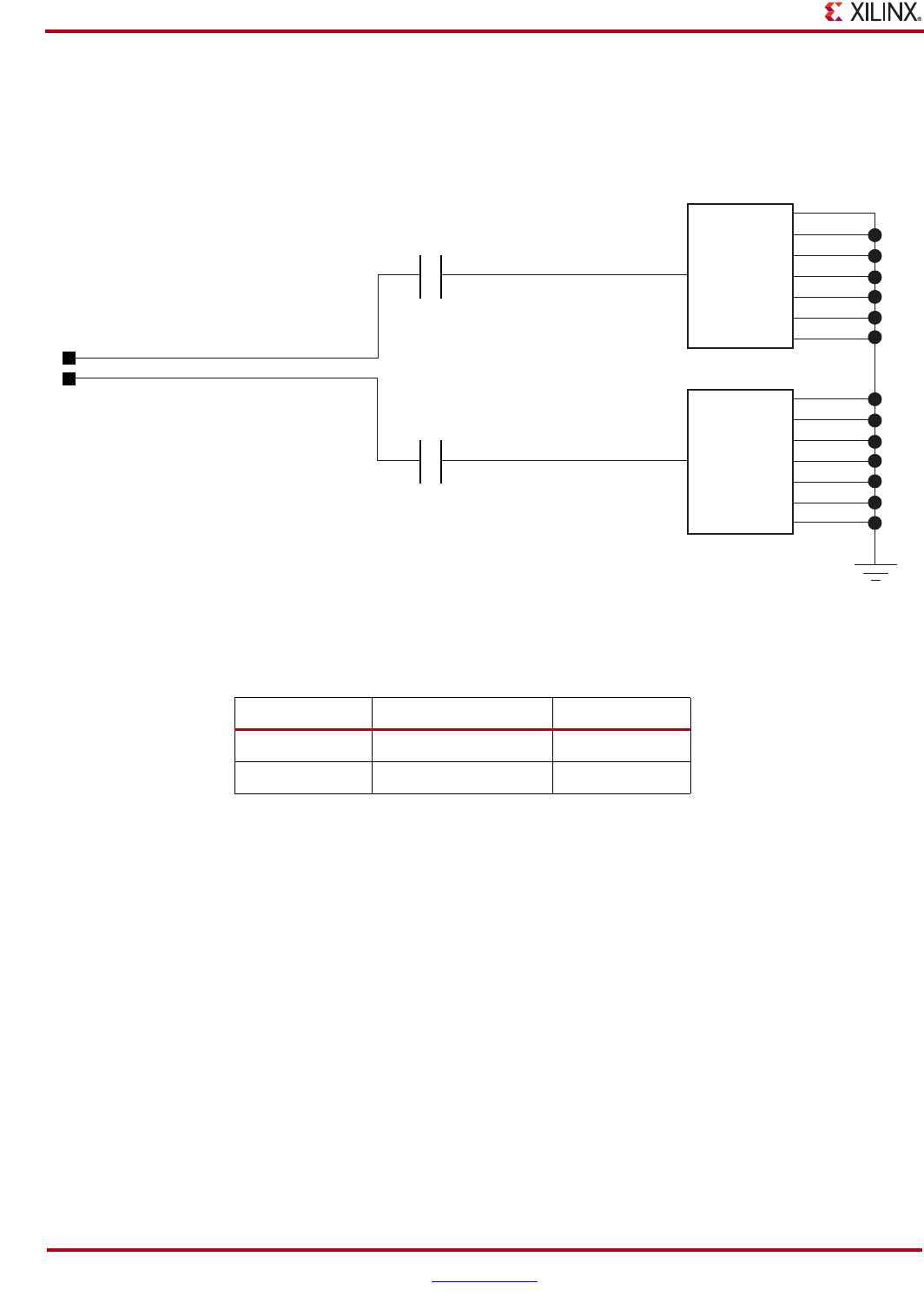
15. IIC Bus
The ML605 implements four IIC bus interfaces at the FPGA.
The "MAIN" IIC bus hosts four items:
•FPGA U1 Bank 34 "MAIN" IIC interface
•8Kb NV Memory U6
•FMC HPC connector J64
•DDR3 SODIMM Socket J1
The "DVI" IIC bus hosts two items:
•FPGA U1 Bank 34 "DVI" IIC interface
•DVI codec U38 and DVI connector J63
The "LPC" IIC bus hosts two items:
•FPGA U1 Bank 33 "LPC" IIC interface
•FMC LPC connector J63
The "SFP" IIC bus hosts two items:
•FPGA U1 Bank 13 "SFP" IIC interface
•SFP module connector P4
The ML605 IIC bus topology is shown in Figure 1-14.
ML605 Hardware User Guide www.xilinx.com 43
UG534 (v1.2.1) January 21, 2010
Detailed Description
X-Ref Target - Figure 1-14
Figure 1-14: IIC Bus Topology
U1
J63
P3
U38
BANK 34
IIC_SDA_MAIN_LS
IIC_SCL_MAIN_LS
IIC_SDA_SFP
IIC_SCL_SFP
IIC_SDA_DVI
IIC_SCL_DVI
FMC_LPC_IIC_SDA_LS
FMC_LPC_IIC_SCL_LS
FMC_LPC_IIC_SCL
U6
J64
J1
FMC_LPC_IIC_SDA
IIC_CLK_DVI_F IIC_SCL_MAIN
ST MICRO
M24C08-WDW6TP
FMC HPC
COLUMN C
2 Kb EEPROM on
any FMC LPC
Mezzanine Card
DDR3 SODIMM
SOCKET
P4
SFP MODULE
CONNECTOR
IIC_SDA_MAIN
SFP_MOD_DEF2
SFP_MOD_DEF1
IIC_SDA_DVI_F
BANK 13
BANK 34
BANK 33
FPGA IIC
INTERFACE
FMC LPC
COLUMN C
2 Kb EEPROM on
any FMC LPC
Mezzanine Card
Addr: 0b1010001
Addr: 0b1010000
Addr: 0b1110110
Addr: 0b1010100
through
0b1010111
Addr: 0b1010000
Addr: 0b1010000
Addr: 0b1010011
2 Kb EEPROM
Addr: 0b0011011
Temperature Sensor
DVI CONN
DVI CODEC
CHRONTEL
CH730C-TF
LEVEL
SHIFTER
UG534_14_092109
LEVEL
SHIFTER
LEVEL
SHIFTER
LEVEL
SHIFTER
44 www.xilinx.com ML605 Hardware User Guide
UG534 (v1.2.1) January 21, 2010
Chapter 1: ML605 Evaluation Board
8 Kb NV Memory
The ML605 hosts an 8 Kb ST Microelectronics M24C08-WDW6TP IIC parameter storage
memory device (U6). The IIC address of U7 is 0b1010100, and U6 is not write protected
(WP pin 7 is tied to GND).
The IIC memory is shown in Figure 1-15.
References
See the ST Micro M24C08 Data Sheet for more information. [Ref 31]
In addition, see the Xilinx XPS IIC Bus Interface (v2.00a) Data Sheet. [Ref 21]
X-Ref Target - Figure 1-15
Figure 1-15: IIC Memory U6
UG534_15_072109
IIC SCL MAIN
VCC3V3
VCC3V3VCC3V3
IIC Address = 0b1010100
IIC SDA MAIN
U6
SCL
WP C65
X5R
10V
0.1UF
VCC
GND
SDA
A0
A1
A2
6
7
8
4
5
1
1
2
M24C08-WDW6TP
2
3
R305
DNP
1%
1/16W
R413
0
5%
1/16W
R414
0
5%
1/16W
1
1
2
1
1
2
2
05%
2
R414
Table 1-18: IIC Memory Connections
FPGA U1 Pin Schematic Net Name
IIC Memory U6
Pin Number Pin Name
Not Applicable Tied to GND 1 A0
Not Applicable Tied to GND 2 A1
Not Applicable Pulled up (0 ohm) to VCC3V3 3 A2
N10 IIC_SDA_MAIN 5 SDA
P11 IIC_SCL_MAIN 6 SCL
Not Applicable Tied to GND 7 WP
ML605 Hardware User Guide www.xilinx.com 45
UG534 (v1.2.1) January 21, 2010
Detailed Description
16. Status LEDs
Table 1-19 defines the status LEDs.
Table 1-19: Status LEDs
Designator Signal Name Color Label Description
DS1 SYSACE_STAT_LED GREEN System ACE CF
Status LED
System ACE CF Status
DS2 TI_PWRGOOD and
MGT_TI_PWRGOOD
GREEN POWER GOOD Both UCD9240 controllers
report power good
DS13 FPGA_DONE GREEN DONE FPGA configured successfully
DS23 LED_GRN GREEN STATUS USB JTAG Connection Status
(Dual LED)
LED_RED RED
DS25 12V GREEN 12V 12V Power On
DS27 MGT_AVCC GREEN AVCC GD MGT AVCC Power On
DS28 MGT_AVTT GREEN MGT_AVTT MGT AVTT Power On
DS29 DDR3_VTTDDR_PWRGOOD GREEN DDR3 PWR GD DDR3 VTTDDR Power Good
DS30 SYSACE_ERR_LED RED System ACE CF
Error LED
System ACE CF Error
DS31 FPGA_INIT_B RED INIT FPGA Initialization in progress
DS32 DVI_GPIO1_FMC_C2M_PG GREEN FMC PWR GD FMC Power Good
46 www.xilinx.com ML605 Hardware User Guide
UG534 (v1.2.1) January 21, 2010
Chapter 1: ML605 Evaluation Board
Ethernet PHY Status LEDs
The Ethernet PHY status LEDs are mounted to be visible when the ML605 board is
installed into a PC motherboard. They are mounted in right-angle, plastic housings and
can be seen on the connector end of the board. This cluster of six LEDs is installed adjacent
to the RJ45 Ethernet jack P2.
X-Ref Target - Figure 1-16
Figure 1-16: Ethernet PHY Status LEDs
Direction
Indicator
Link Rate
(Mbps)
DUP
TX
RX
10
100
1000
P2
End view of ML605 Ethernet jack and
status LEDs when installed vertically
in a PC chassis
UG534_16_101209
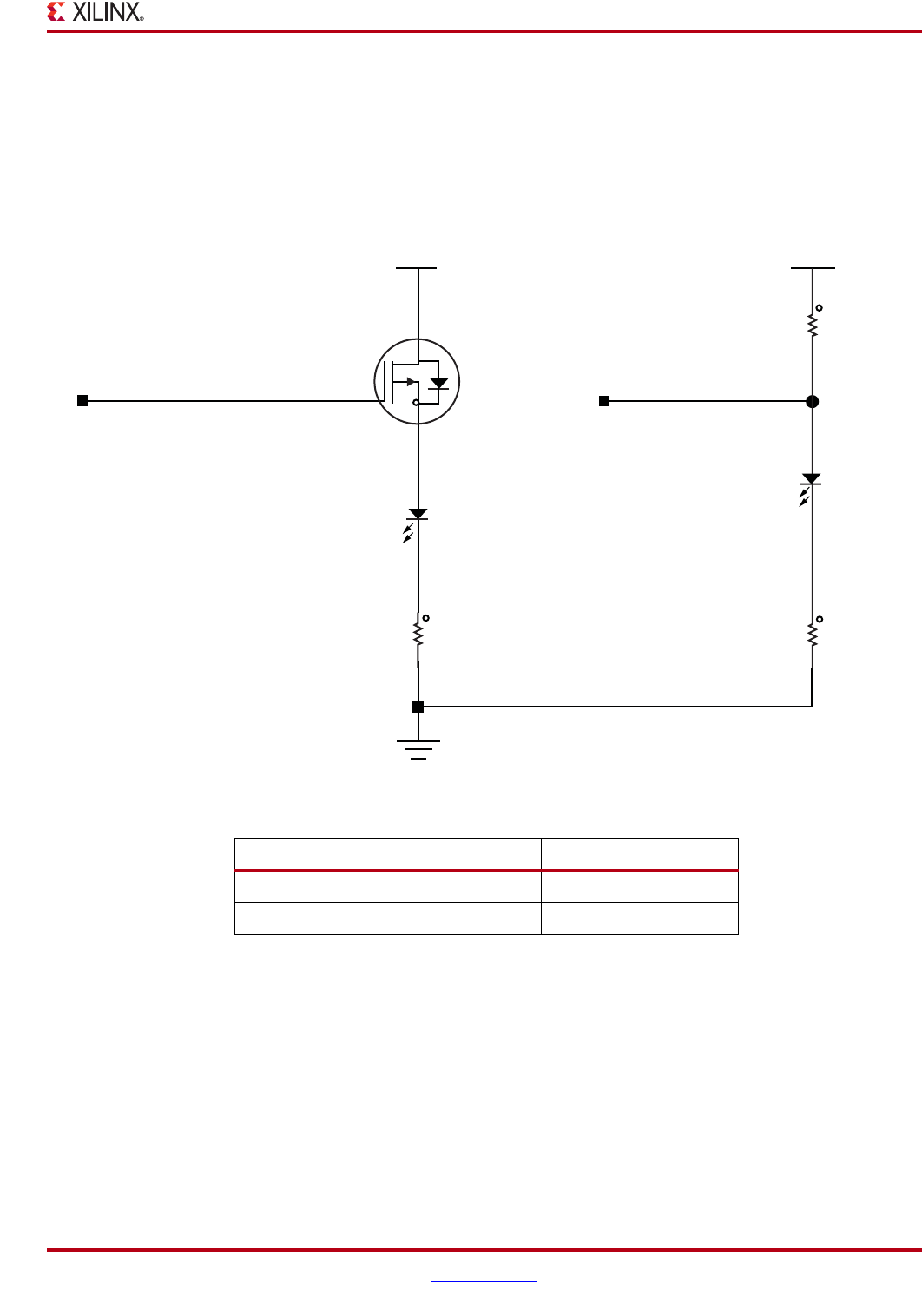
ML605 Hardware User Guide www.xilinx.com 47
UG534 (v1.2.1) January 21, 2010
Detailed Description
FPGA INIT and DONE LEDs
The typical Xilinx FPGA power up and configuration status LEDs are present on the
ML605.
The red INIT LED DS31 comes on momentarily after the FPGA powers up and during its
internal power-on process. The DONE LED DS13 comes on after the FPGA programming
bitstream has been downloaded and the FPGA successfully configured.
17. User I/O
The ML605 provides the following user and general purpose I/O capabilities:
•User LEDs (8) with parallel wired GPIO male pin header
•User Pushbutton (5) switches with associated direction LEDs
•CPU Reset pushbutton switch
•User DIP switch (8-pole)
•User SMA GPIO
•LCD Display (16 char x 2 lines)
X-Ref Target - Figure 1-17
Figure 1-17: FPGA INIT and DONE LEDs
FPGA INIT B
NDS336P
FPGA_DONE
VCC2V5 VCC2V5
Q14
1
R419
330
5%
1/16W
R4
27.4
1%
1/16W
R3
27.4
1%
1/16W
1
2
1
2
1
2
DS31
DS13
32
12
12
LED-RED-SMT
LED-GRN-SMT
UG534_17_011310
Table 1-20: FPGA INIT and DONE LED Connections
FPGA U1 Pin Schematic Net Name Controlled LED
P8 FPGA_INIT_B DS31 INIT, Red
R8 FPGA_DONE DS13 DONE, Green
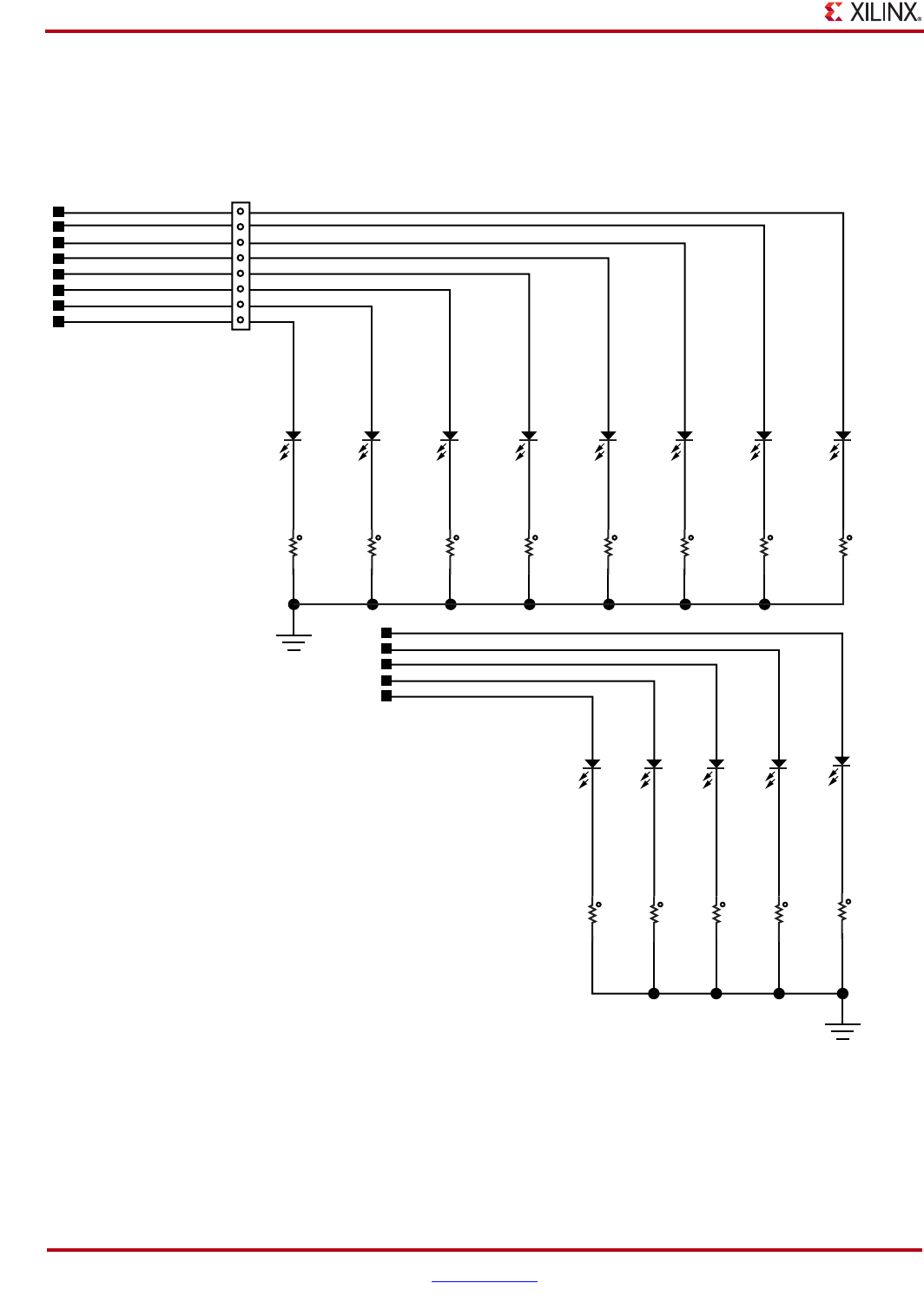
48 www.xilinx.com ML605 Hardware User Guide
UG534 (v1.2.1) January 21, 2010
Chapter 1: ML605 Evaluation Board
User LEDs
The ML605 provides two groups of active-High LEDs as described in Figure 1-18 and
Table 1-21.
Note: See “User Pushbutton Switches,” page 49 for more details about the LEDs.
X-Ref Target - Figure 1-18
Figure 1-18: User LEDs and GPIO Connector, Directional LEDs
GPIO_LED_C
GPIO_LED_6
GPIO_LED_7
GPIO_LED_5
GPIO_LED_4
GPIO_LED_3
GPIO_LED_2
GPIO_LED_1
GPIO_LED_0 1
2
3
4
5
6
7
8
J62
H-1X8
GPIO_LED_W
GPIO_LED_E
GPIO_LED_S
GPIO_LED_N
R12
27.4
1%
1/16W
R17
27.4
1%
1/16W
R16
27.4
1%
1/16W
R15
27.4
1%
1/16W
R14
27.4
1%
1/16W
R13
27.4
1%
1/16W
R11
27.4
1%
1/16W
R10
27.4
1%
1/16W
R9
27.4
1%
1/16W
R8
27.4
1%
1/16W
R7
27.4
1%
1/16W
R6
27.4
1%
1/16W
R5
27.4
1%
1/16W
1
2
1
2
1
2
1
2
1
2
1
2
1
2
1
2
1
2
1
2
1
2
1
2
1
2
UG534_18_081109
GPIO_LED_N_R
GPIO_LED_S_R
GPIO_LED_E_R
GPIO_LED_W_R
GPIO_LED_C_R
LED-GRN-SMT
DS16
1
1
2
LED-GRN-SMT
DS12
12
LED-GRN-SMT
DS11
12
LED-GRN-SMT
DS9
12
LED-GRN-SMT
DS10
12
LED-GRN-SMT
DS15
12
LED-GRN-SMT
DS14
12
LED-GRN-SMT
DS22
12
LED-GRN-SMT
DS21
12
LED-GRN-SMT
DS17
2
1
LED-GRN-SMT
DS19
2
1
LED-GRN-SMT
DS18
2
1
LED-GRN-SMT
DS20
2
This group of LEDs is mounted
adjacent to their respective “direction”
pushbuttons, as seen on the right side
of the LCD on the board photo (Figure
1-2).
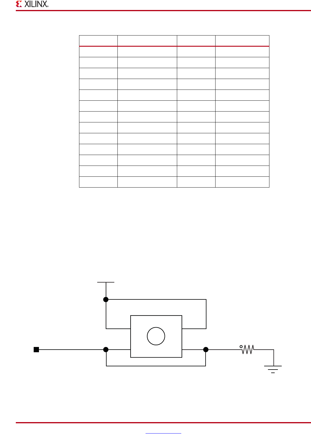
ML605 Hardware User Guide www.xilinx.com 49
UG534 (v1.2.1) January 21, 2010
Detailed Description
User Pushbutton Switches
The ML605 provides six active-High pushbutton switches:
•SW5, SW6, SW7, SW8 and SW9, arranged in a diamond configuration to depict
“directional” headings North, South, East, West and Center respectively
•SW10 CPU Reset pushbutton
The six pushbuttons all have the same active-High topology as the sample shown in
Figure 1-19. The five directional pushbuttons are assigned as GPIO and the sixth is assigned
as CPU_RESET. Figure 1-19 and Table 1-22, page 50 describe the pushbutton switches.
Table 1-21: User LED Connections
FPGA U1 Pin Schematic Net Name GPIO J62 Pin Controlled LED
AC22 GPIO_LED_0 1 DS12
AC24 GPIO_LED_1 2 DS11
AE22 GPIO_LED_2 3 DS9
AE23 GPIO_LED_3 4 DS10
AB23 GPIO_LED_4 5 DS15
AG23 GPIO_LED_5 6 DS14
AE24 GPIO_LED_6 7 DS22
AD24 GPIO_LED_7 8 DS21
AP24 GPIO_LED_C – DS16
AD21 GPIO_LED_W – DS17
AE21 GPIO_LED_E – DS19
AH28 GPIO_LED_S – DS18
AH27 GPIO_LED_N – DS20
X-Ref Target - Figure 1-19
Figure 1-19: User Pushbutton Switch (Typical)
CPU RESET
VCC1V5
Pushbutton
1
4.7K
R401
5%
1/16W
sw10
2
4
3
1
2
P1
P2
P4
P3
UG534_19_072109
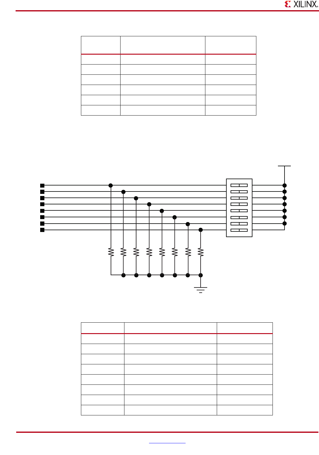
50 www.xilinx.com ML605 Hardware User Guide
UG534 (v1.2.1) January 21, 2010
Chapter 1: ML605 Evaluation Board
User DIP Switch
The ML605 includes an active-High eight pole DIP switch as described in Figure 1-20 and
Table 1-23.
Table 1-22: User Pushbutton Switch Connections
U1 FPGA Pin Schematic Net Name Pushbutton
Switch Pin
A19 GPIO_SW_N SW5.2
A18 GPIO_SW_S SW6.2
G17 GPIO_SW_E SW7.2
H17 GPIO_SW_W SW8.2
G26 GPIO_SW_C SW9.2
H10 CPU_RESET SW10.2
X-Ref Target - Figure 1-20
Figure 1-20: User 8-pole DIP Switch
UG534_20_072109
GPIO DIP SW1
GPIO DIP SW2
GPIO DIP SW3
GPIO DIP SW4
GPIO DIP SW5
GPIO DIP SW6
GPIO DIP SW7
GPIO DIP SW8
1
2
3
4
5
6
7
8
16
SW1
VCC1V5
SDMX-8-X
15
14
13
12
11
10
9
67
8
9
10
2
3
4
5
RP7
4.7K
6RP7
4.7K
6RP7
4.7K
6
1
RP7
RP7
4.7K
1RP7
4.7K
1RP7
4.7K
1RP7
4.7K
4.7K 5%
5%
5%
5%
5%
5%
5%
5%
Table 1-23: User DIP Switch Connections
U1 FPGA Pin Schematic Net Name DIP Switch Pin
D22 GPIO_DIP_SW1 SW1.1
C22 GPIO_DIP_SW2 SW1.2
L21 GPIO_DIP_SW3 SW1.3
L20 GPIO_DIP_SW4 SW1.4
C18 GPIO_DIP_SW5 SW1.5
B18 GPIO_DIP_SW6 SW1.6
K22 GPIO_DIP_SW7 SW1.7
K21 GPIO_DIP_SW8 SW1.8
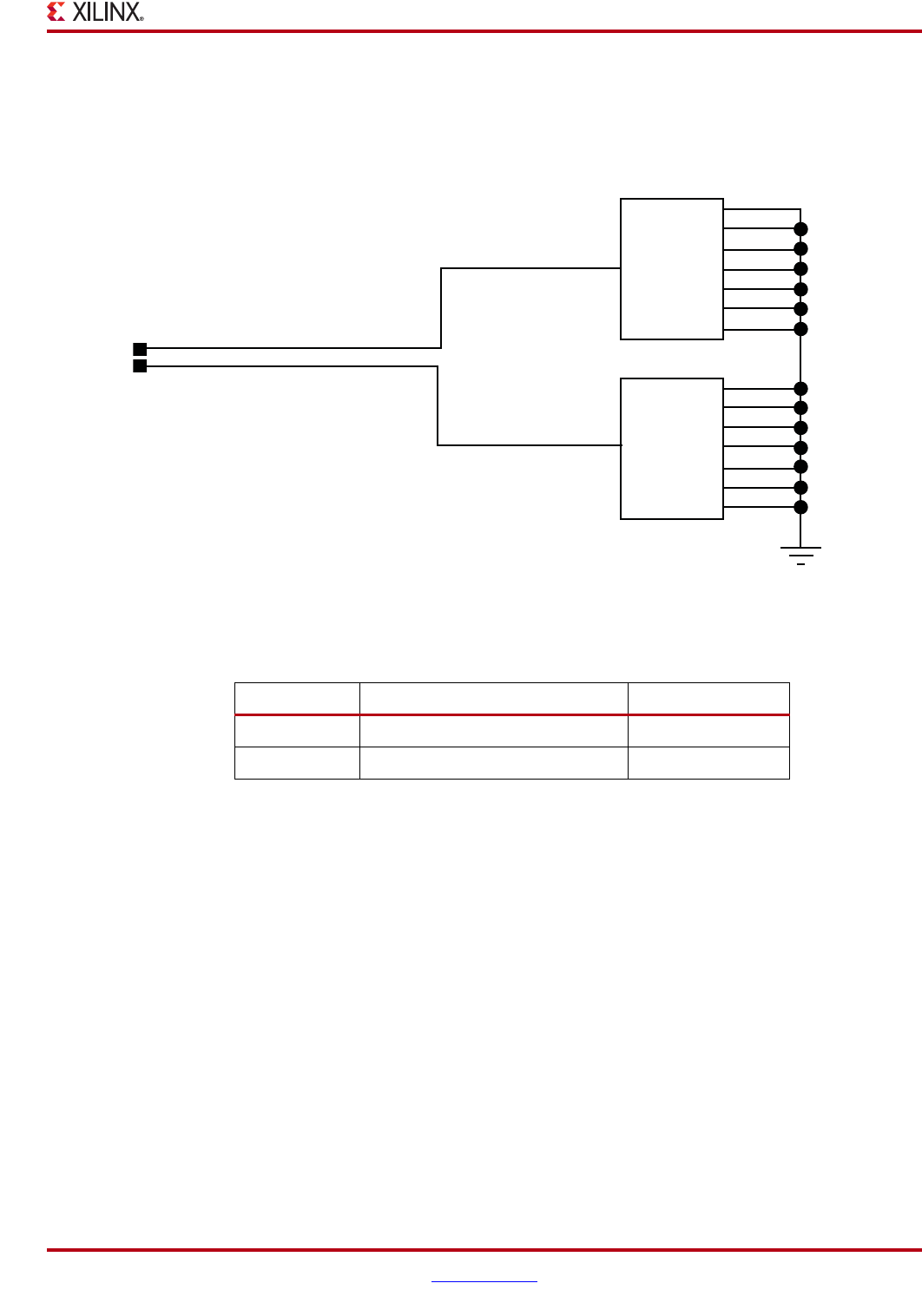
ML605 Hardware User Guide www.xilinx.com 51
UG534 (v1.2.1) January 21, 2010
Detailed Description
User SMA GPIO
The ML605 includes an pair of SMA connectors for GPIO as described in Figure 1-21 and
Table 1-24.
X-Ref Target - Figure 1-21
Figure 1-21: User SMA GPIO
UG534_21_072109
USER SMA GPIO N
J56 32K10K-400E3
J76 32K10K-400E3
GND1
SIG
1
1
SIG
GND2
GND3
GND4
GND5
GND6
GND7
GND1
GND2
GND3
GND4
GND5
GND6
GND7
USER SMA GPIO P
2
3
4
5
6
7
8
2
3
4
5
6
7
8
Table 1-24: User SMA Connections
U1 FPGA Pin Schematic Net Name SMA Pin
W34 USER_SMA_GPIO_N J56.1
V34 USER_SMA_GPIO_P J57.1
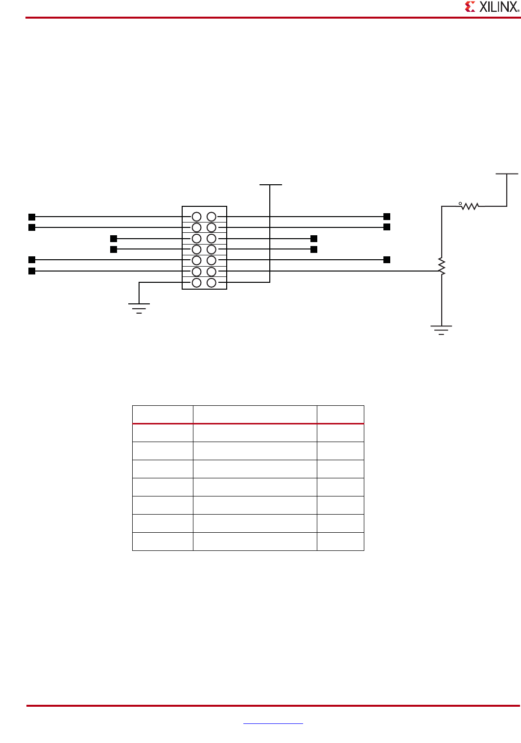
52 www.xilinx.com ML605 Hardware User Guide
UG534 (v1.2.1) January 21, 2010
Chapter 1: ML605 Evaluation Board
LCD Display (16 Character x 2 Lines)
The ML605 board has a 16-character x 2-line LCD (Display Tech S162D BA BC, installed
onto J41 2x7 header) on the board to display text information. Potentiometer R270 adjusts
the contrast of the LCD. A ST2378E (U33) 2.5V-to-5V level-shifter is used to shift the
voltage level between the FPGA and the LCD. The data interface to the LCD is connected
to the FPGA to support 4-bit mode only. The LCD module has a connector that allows the
LCD to be removed from the board to access to the components below it.
Caution! Care should be taken not to scratch or damage the surface of the LCD window.
X-Ref Target - Figure 1-22
Figure 1-22: LCD Header J41 and Contrast Trimpot R270
LCD_DB7
LCD_DB5
LCD_E
LCD_RS
NC
NC
NC
LCD_DB6
LCD_DB4
LCD_RW
LCD_VEE
NC
VCC5
VCC5
SSW-107-01-T-D
1
J41
2
34
56
78
910
11 12
1314
32
32
32
2
1%
silkscreen:
“LCD Contrast”
R270
0-2K
1/2W
20%
R158
6.81K
13
2
1
UG534_22_073109
Table 1-25: LCD Header Connections
U1 FPGA Pin Schematic Net Name J41 Pin
AD14 LCD_DB4_LS 4
AK11 LCD_DB5_LS 3
AJ11 LCD_DB6_LS 2
AE12 LCD_DB7_LS 1
AC14 LCD_RW_LS 10
T28 LCD_RS_LS 11
AK12 LCD_E_LS 9
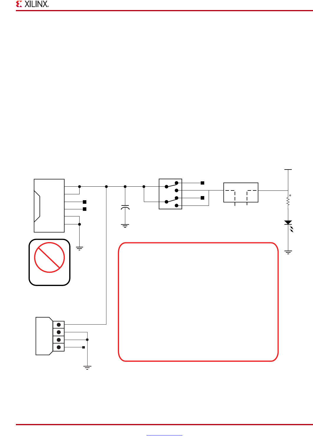
ML605 Hardware User Guide www.xilinx.com 53
UG534 (v1.2.1) January 21, 2010
Detailed Description
18. Switches
The ML605 Evaluation board includes the following switches:
•Power On/Off Slide Switch SW2
•FPGA_PROG_B SW4 (active-Low)
•SYSACE_RESET_B SW3 (active-Low)
•System ACE CF CompactFlash Image Select DIP Switch S1 (active-High)
•MODE, Boot EEPROM Select and CCLK Osc Enable DIP switch S2 (active-High)
Power On/Off Slide Switch SW2
SW2 is the ML605 board main power on/off switch. Sliding the switch actuator from the
off to on position applies 12V power from either J60 (6-pin Mini-Fit) or J25 (4-pin ATX)
power connector to the VCC12_P power plane via the 1mΩ 1% 3W series current sense
resistor R346. See “22. System Monitor,” page 68 for further details on 12V input current
sensing. Green LED DS25 will illuminate when the ML605 board power is on. See section
“21. Power Management,” page 65 for details on the onboard power system.
X-Ref Target - Figure 1-23
Figure 1-23: Power On/Off Slide Switch SW2
UG534_23 _081209
N/C
12v
12v
N/C
COM
COM
1
4
2
3
6
1
2
3
4
5
NC
NC
39-30-1060
ATX Peripheral Cable Connector
can plug into J25 when ML605 is
in PC and the desk top AC adapter
(brick) is not used.
J25
J60
12V
COM
COM
5V NC
350211-1
VCC12_P_IN
1
2NC
NC
DPDT
VCC12_P
5
2
+C280
330UF
16V
ELEC
1
3
4
6
SW2
1201M2S3ABE2
R346
I1
E1
E1
E2
E2
I2
0.001R
I2I1
3W
0.5%
Y14880R00100B09R
12
2
1R322
1.00K
1%
1/16W
DS25
LED-GRN-SMT
CAUTION!
DO NOT plug a PC ATX power supply 6-pin connector into
the J60 connector on the ML605 board. The ATX 6-pin
connector has a different pinout than J60 and will damage
the ML605 board and void the board warranty.
DO NOT plug an auxilliary PCIe 6-pin molex power
connector into the J60 connector as this could damage the
PCIe motherboard and/or the ML605 board. J60 is marked
with a NO PCIE POWER label to warn users of the poten-
tial hazard.
DO NOT apply power to J60 and the 4-pin ATX disk drive
connector J25 at the same time as this will damage the
ML605 board.
PCIe
Power
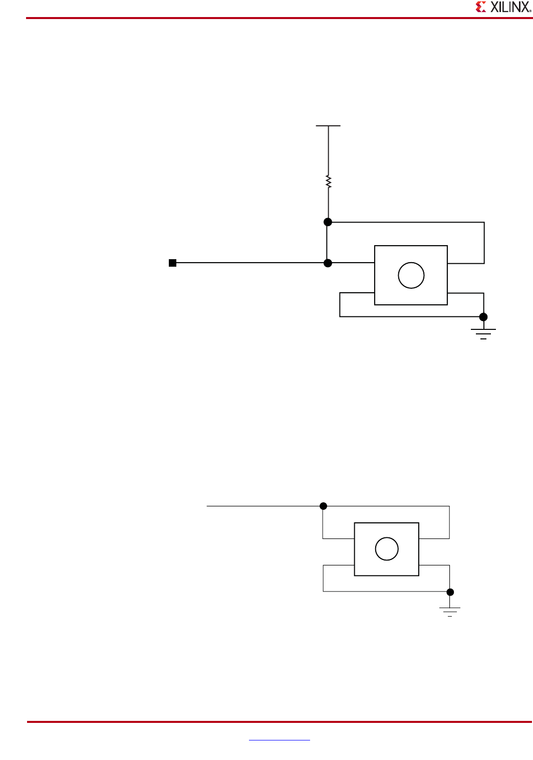
54 www.xilinx.com ML605 Hardware User Guide
UG534 (v1.2.1) January 21, 2010
Chapter 1: ML605 Evaluation Board
FPGA_PROG_B Pushbutton SW4 (Active-Low)
This switch grounds the FPGA's PROG_B pin when pressed. This action clears the FPGA.
See the Virtex-6 FPGA Data Sheet for more information on clearing the contents of the
FPGA. [Ref 4]
SYSACE_RESET_B Pushbutton SW3 (Active-Low)
When the System ACE CF configuration mode pin is high (enabled by closing DIP switch
S1 switch 4), the System ACE CF controller configures the FPGA from the CompactFlash
card when a card is inserted or the SYSACE RESET button is pressed. See “5. System ACE
CF and CompactFlash Connector,” page 24 for more details.
X-Ref Target - Figure 1-24
Figure 1-24: FPGA PROG_B Pushbutton SW4
FPGA_PROG_B
FPGA PROG
Pushbutton
Silkscreen:
PROG
VCC2V5
RP4
4.7K
14
5%
1P1
P2
P4
P3
2
4
3
SW4
UG534_24_073109
X-Ref Target - Figure 1-25
Figure 1-25: System ACE CF RESET_B Pushbutton SW3
Pushbutton
silkscreen:
“SYSACE RESET”
SYSACE_RESET_B
1
SW3
2
4
3
P1
P2
P4
P3
UG534_25_073109
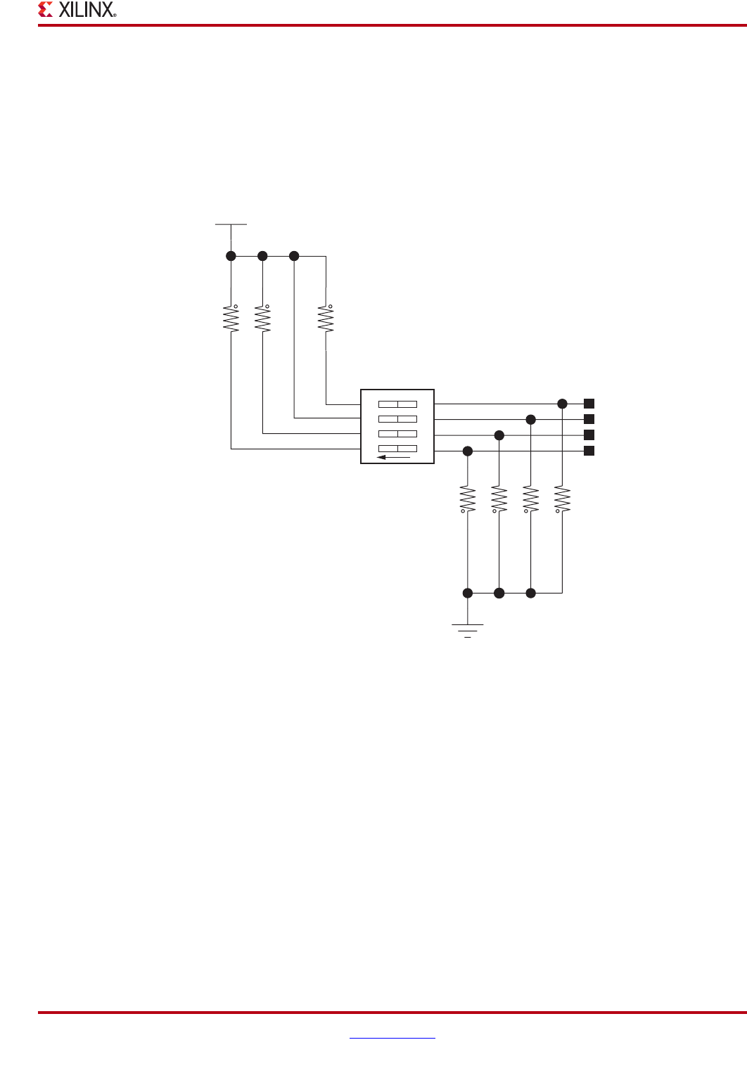
ML605 Hardware User Guide www.xilinx.com 55
UG534 (v1.2.1) January 21, 2010
Detailed Description
System ACE CF CompactFlash Image Select DIP Switch S1
System ACE CF CompactFlash (CF) image select DIP switch S1, switches 1–3, select which
CF resident bitstream image is downloaded to the FPGA (Figure 1-26). S1 switches 1–3
offer eight binary addresses. When ON (High), the S1 switch 4 enables the System ACE CF
controller to configure the FPGA from the CF card when a card is inserted or when the
SYSACE RESET button is pressed. See “5. System ACE CF and CompactFlash Connector,”
page 24 for more details about the System ACE controller.
Note: S1 switch 4 is the System ACE controller enable switch. When ON, this switch allows the
System ACE to boot at power-on if it finds a CF card present. In order to boot from BPI Flash U4 or
Xilinx Platform Flash (U27) without System ACE contention, S1 switch 4 must be OFF.
X-Ref Target - Figure 1-26
Figure 1-26: System ACE CF CompactFlash Image Select DIP Switch S1
UG534_26_110409
SDMX-4-X
VCC2V5
1
2
5% 1/16W
510
R55
R64 510
510
1/16W
5%
1
2
5% 1/16W
R63
2
1
R62
510
1/16W
5%
1
2
R60
1.00K
1/16W
1%
1
2
R58
1.00K
1/16W
1%
2
1
1%
1/16W
1.00K
R59
2
1
1%
1/16W
1.00K
R61
SYSACE_CFGMODEPIN
SYSACE_CFGADDR1
SYSACE_CFGADDR2
SYSACE_CFGADDR0
1
2
3
4
1234
8
7
6
5
S1
ON
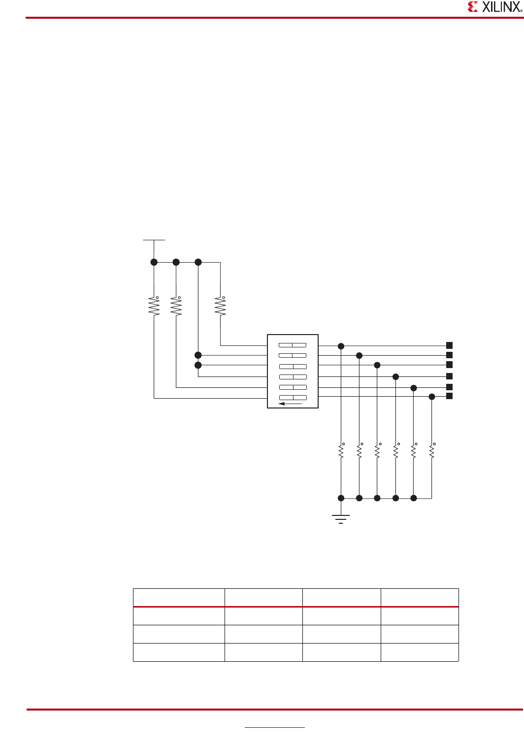
56 www.xilinx.com ML605 Hardware User Guide
UG534 (v1.2.1) January 21, 2010
Chapter 1: ML605 Evaluation Board
Mode, Osc Enable, Boot EEPROM Select, and Addr Select DIP Switch S2
DIP switch S2 is a multi-purpose selector switch (Figure 1-27 and Table 1-27, page 57).
FPGA Mode: S2 switches 3, 4, and 5 control the FPGA mode (Table 1-26).
Oscillator Enable: S2 switch 1, CCLK_EXTERNAL, controls the enable pin of the 47 MHz
oscillator SiT8102 (X4). When switch 1 is closed (CCLK_EXTERNAL High), X4 drives a
47 MHz clock onto the FPGA_CCLK signal.
Boot EEPROM Select: S2 switch 2 is used to select the between the Xilinx Platform Flash or
the Numonyx Linear BPI Flash for the FPGA boot memory device.
Upper or Lower Address Select: S2 switch 6 is used to select the upper or lower half of
flash memory U4 as the source of the FPGA bitstream image. When FLASH_A23 is High,
the upper half of the address is selected. When FLASH_A23 is Low, the lower half of the
address is selected.
Table 1-26 shows the FPGA configuration modes controlled by S2 switches 3, 4, and 5.
X-Ref Target - Figure 1-27
Figure 1-27: Multi-Purpose Select DIP Switch S2
Table 1-26: ML605 Configuration Modes
Configuration Mode M[2:0] Bus Width CCLK
Master BPI-Up 010 8, 16 Output
JTAG 101 1 Input (TCK)
Slave SelectMAP 110 8, 16, 32 Input
UG534_27_110409
SDMX-6-X
4
5
6
123456
9
8
7
1
2
3
12
11
10
S2
ON
VCC2V5
1
2
5%
1/16W
510
R57
1/16W
5%
1
2
5%
1/16W
510
R52
2
1
R51
510
1/16W
5%
CCLK EXTERNAL
P30_CS_SEL
FPGA_M0
FPGA_M1
FPGA_M2
FLASH_A23
1
2
1
2
1
2
1
2
1
2
1
2
1/16w
5%
1/16w
5%
1/16w
5%
1/16w
5%
1/16w
5%
1/16w
5%
R43
R50
R53
R54
R55
R56
4.7K
4.7K
4.7K
4.7K
4.7K
4.7K
ML605 Hardware User Guide www.xilinx.com 57
UG534 (v1.2.1) January 21, 2010
Detailed Description
See “3. 128 Mb Platform Flash XL,” page 20 and “4. 32 MB Linear BPI Flash,” page 20 for
details.
19. VITA 57.1 FMC HPC Connector
The ML605 implements both the High Pin Count (HPC, J64) and Low Pin Count (LPC, J63)
connector options of VITA 57.1.1 FMC specification. This section discusses the FMC HPC
J64 connector.
The FMC standard calls for two connector densities: a High Pin Count (HPC) and a Low
Pin Count (LPC) implementation. A common 10 x 40 position (400 pin locations) connector
form factor is used for both versions. The HPC version is fully populated with 400 pins
present, and the LPC version is partially populated with 160 pins.
The 10 x 40 rows of a FMC HPC connector provides connectivity for:
•160 single-ended or 80 differential user-defined signals
•10 MGTs
•2 MGT clocks
•4 differential clocks
•159 ground, 15 power connections
Of the above signal and clock connectivity capability, the ML605 implements the following
subset:
•78 differential user defined pairs:
♦34 LA pairs
♦24 HA pairs
♦20 HB pairs
•8 MGTs
•2 MGT clocks
•4 differential clocks
Table 1-27: Switch S2 Configuration Details
Switch Configuration Mode/Method
Switch Net Name JTAG
System ACE CF
Slave SelectMAP
Platform Flash XL
Master BPI
P30 Linear Flash
S2.1 CCLK_EXTERNAL Off On Off
S2.2 P30_CS_SEL On(1) Off On
S2.3 FPGA_M0 On Off Off
S2.4 FPGA_M1 Off On On
S2.5 FPGA_M2 On On Off
S2.6 FLASH_A23 Off Don't Care Off(2)
Notes:
1. In JTAG mode, S2.2 is shown as ON for FPGA access to the P30 Linear Flash. Alternatively, set S2.2 to
OFF for FPGA access to the Platform Flash XL.
2. In Master BPI mode, S2.6 is shown as OFF for selecting initial configuration from BPI address
0x000000. Alternatively, set S2.6 to ON to select initial configuration from BPI address 0x800000.
58 www.xilinx.com ML605 Hardware User Guide
UG534 (v1.2.1) January 21, 2010
Chapter 1: ML605 Evaluation Board
Note: The ML605 board VADJ voltage for the FMC HPC and LPC connectors (J64 and J63) is fixed
at 2.5V (non-adjustable). The 2.5V rail cannot be turned off. The ML605 VITA 57.1 FMC interfaces
are compatible with 2.5V mezzanine cards capable of supporting 2.5V VADJ.
Table 1-28 shows the VITA 57.1 FMC HPC connections. The connector pinout is in
Appendix B, “VITA 57.1 FMC LPC (J63) and HPC (J64) Connector Pinout.”
Any signal named FMC_HPC_xxxx that is wired between a U1 FPGA pin and some other
device does not appear in this table.
Table 1-28: VITA 57.1 FMC HPC Connections
J64 FMC
HPC Pin Schematic Net Name U1 FPGA
Pin
J64 FMC
HPC Pin Schematic Net Name U1 FPGA
Pin
A2 FMC_HPC_DP1_M2C_P AE3 B12 FMC_HPC_DP7_M2C_P AP5
A3 FMC_HPC_DP1_M2C_N AE4 B13 FMC_HPC_DP7_M2C_N AP6
A6 FMC_HPC_DP2_M2C_P AF5 B16 FMC_HPC_DP6_M2C_P AM5
A7 FMC_HPC_DP2_M2C_N AF6 B17 FMC_HPC_DP6_M2C_N AM6
A10 FMC_HPC_DP3_M2C_P AG3 B20 FMC_HPC_GBTCLK1_M2C_P AK6
A11 FMC_HPC_DP3_M2C_N AG4 B21 FMC_HPC_GBTCLK1_M2C_N AK5
A14 FMC_HPC_DP4_M2C_P AJ3 B32 FMC_HPC_DP7_C2M_P AP1
A15 FMC_HPC_DP4_M2C_N AJ4 B33 FMC_HPC_DP7_C2M_N AP2
A18 FMC_HPC_DP5_M2C_P AL3 B36 FMC_HPC_DP6_C2M_P AN3
A19 FMC_HPC_DP5_M2C_N AL4 B37 FMC_HPC_DP6_C2M_N AN4
A22 FMC_HPC_DP1_C2M_P AD1
A23 FMC_HPC_DP1_C2M_N AD2
A26 FMC_HPC_DP2_C2M_P AF1
A27 FMC_HPC_DP2_C2M_N AF2
A30 FMC_HPC_DP3_C2M_P AH1
A31 FMC_HPC_DP3_C2M_N AH2
A34 FMC_HPC_DP4_C2M_P AK1
A35 FMC_HPC_DP4_C2M_N AK2
A38 FMC_HPC_DP5_C2M_P AM1
A39 FMC_HPC_DP5_C2M_N AM2
C2 FMC_HPC_DP0_C2M_P AB1 D4 FMC_HPC_GBTCLK0_M2C_P AD6
C3 FMC_HPC_DP0_C2M_N AB2 D5 FMC_HPC_GBTCLK0_M2C_N AD5
C6 FMC_HPC_DP0_M2C_P AC3 D8 FMC_HPC_LA01_CC_P AK19
C7 FMC_HPC_DP0_M2C_N AC4 D9 FMC_HPC_LA01_CC_N AL19
C10 FMC_HPC_LA06_P AG20 D11 FMC_HPC_LA05_P AG22
C11 FMC_HPC_LA06_N AG21 D12 FMC_HPC_LA05_N AH22
ML605 Hardware User Guide www.xilinx.com 59
UG534 (v1.2.1) January 21, 2010
Detailed Description
C14 FMC_HPC_LA10_P AM20 D14 FMC_HPC_LA09_P AM18
C15 FMC_HPC_LA10_N AL20 D15 FMC_HPC_LA09_N AL18
C18 FMC_HPC_LA14_P AN19 D17 FMC_HPC_LA13_P AP19
C19 FMC_HPC_LA14_N AN20 D18 FMC_HPC_LA13_N AN18
C22 FMC_HPC_LA18_CC_P AH25 D20 FMC_HPC_LA17_CC_P AN27
C23 FMC_HPC_LA18_CC_N AJ25 D21 FMC_HPC_LA17_CC_N AM27
C26 FMC_HPC_LA27_P AP30 D23 FMC_HPC_LA23_P AL26
C27 FMC_HPC_LA27_N AP31 D24 FMC_HPC_LA23_N AM26
C30 IIC_SCL_MAIN_LS(1) AK9 D26 FMC_HPC_LA26_P AM25
C31 IIC_SDA_MAIN_LS(1) AE9 D27 FMC_HPC_LA26_N AL25
D29 FMC_HPC_TCK_BUF(2) U88.15
D30 FMC_TDI_BUF(2) J17.1
D31 FMC_HPC_TDO(2) J17.3
D33 FMC_TMS_BUF(2) U88.17
E2 FMC_HPC_HA01_CC_P AD29 F1 FMC_HPC_PG_M2C_LS(1) J27
E3 FMC_HPC_HA01_CC_N AC29 F4 FMC_HPC_HA00_CC_P AE33
E6 FMC_HPC_HA05_P AB27 F5 FMC_HPC_HA00_CC_N AF33
E7 FMC_HPC_HA05_N AC27 F7 FMC_HPC_HA04_P AB28
E9 FMC_HPC_HA09_P AB30 F8 FMC_HPC_HA04_N AC28
E10 FMC_HPC_HA09_N AB31 F10 FMC_HPC_HA08_P AG31
E12 FMC_HPC_HA13_P AE31 F11 FMC_HPC_HA08_N AF31
E13 FMC_HPC_HA13_N AD31 F13 FMC_HPC_HA12_P AD32
E15 FMC_HPC_HA16_P AC33 F14 FMC_HPC_HA12_N AE32
E16 FMC_HPC_HA16_N AB33 F16 FMC_HPC_HA15_P AB32
E18 FMC_HPC_HA20_P V32 F17 FMC_HPC_HA15_N AC32
E19 FMC_HPC_HA20_N V33 F19 FMC_HPC_HA19_P U33
E21 FMC_HPC_HB03_P AL30 F20 FMC_HPC_HA19_N U32
E22 FMC_HPC_HB03_N AM31 F22 FMC_HPC_HB02_P AP32
E24 FMC_HPC_HB05_P AN33 F23 FMC_HPC_HB02_N AP33
E25 FMC_HPC_HB05_N AN34 F25 FMC_HPC_HB04_P AM33
E27 FMC_HPC_HB09_P AL34 F26 FMC_HPC_HB04_N AL33
Table 1-28: VITA 57.1 FMC HPC Connections (Cont’d)
J64 FMC
HPC Pin Schematic Net Name U1 FPGA
Pin
J64 FMC
HPC Pin Schematic Net Name U1 FPGA
Pin
60 www.xilinx.com ML605 Hardware User Guide
UG534 (v1.2.1) January 21, 2010
Chapter 1: ML605 Evaluation Board
E28 FMC_HPC_HB09_N AK34 F28 FMC_HPC_HB08_P AK33
E30 FMC_HPC_HB13_P AH33 F29 FMC_HPC_HB08_N AK32
E31 FMC_HPC_HB13_N AH32 F31 FMC_HPC_HB12_P AJ31
E33 FMC_HPC_HB19_P AL31 F32 FMC_HPC_HB12_N AJ32
E34 FMC_HPC_HB19_N AK31 F34 FMC_HPC_HB16_P AH29
F35 FMC_HPC_HB16_N AH30
G2 FMC_HPC_CLK1_M2C_P AP20 H2 FMC_HPC_PRSNT_M2C_L(1) AP25
G3 FMC_HPC_CLK1_M2C_N AP21 H4 FMC_HPC_CLK0_M2C_P K24
G6 FMC_HPC_LA00_CC_P AF20 H5 FMC_HPC_CLK0_M2C_N K23
G7 FMC_HPC_LA00_CC_N AF21 H7 FMC_HPC_LA02_P AC20
G9 FMC_HPC_LA03_P AC19 H8 FMC_HPC_LA02_N AD20
G10 FMC_HPC_LA03_N AD19 H10 FMC_HPC_LA04_P AF19
G12 FMC_HPC_LA08_P AK22 H11 FMC_HPC_LA04_N AE19
G13 FMC_HPC_LA08_N AJ22 H13 FMC_HPC_LA07_P AK21
G15 FMC_HPC_LA12_P AM21 H14 FMC_HPC_LA07_N AJ21
G16 FMC_HPC_LA12_N AL21 H16 FMC_HPC_LA11_P AM22
G18 FMC_HPC_LA16_P AP22 H17 FMC_HPC_LA11_N AN22
G19 FMC_HPC_LA16_N AN23 H19 FMC_HPC_LA15_P AM23
G21 FMC_HPC_LA20_P AK23 H20 FMC_HPC_LA15_N AL23
G22 FMC_HPC_LA20_N AL24 H22 FMC_HPC_LA19_P AN25
G24 FMC_HPC_LA22_P AP27 H23 FMC_HPC_LA19_N AN24
G25 FMC_HPC_LA22_N AP26 H25 FMC_HPC_LA21_P AN29
G27 FMC_HPC_LA25_P AN28 H26 FMC_HPC_LA21_N AP29
G28 FMC_HPC_LA25_N AM28 H28 FMC_HPC_LA24_P AN30
G30 FMC_HPC_LA29_P AL28 H29 FMC_HPC_LA24_N AM30
G31 FMC_HPC_LA29_N AK28 H31 FMC_HPC_LA28_P AK27
G33 FMC_HPC_LA31_P AL29 H32 FMC_HPC_LA28_N AJ27
G34 FMC_HPC_LA31_N AK29 H34 FMC_HPC_LA30_P AJ24
G36 FMC_HPC_LA33_P AH23 H35 FMC_HPC_LA30_N AK24
G37 FMC_HPC_LA33_N AH24 H37 FMC_HPC_LA32_P AG25
H38 FMC_HPC_LA32_N AG26
Table 1-28: VITA 57.1 FMC HPC Connections (Cont’d)
J64 FMC
HPC Pin Schematic Net Name U1 FPGA
Pin
J64 FMC
HPC Pin Schematic Net Name U1 FPGA
Pin
ML605 Hardware User Guide www.xilinx.com 61
UG534 (v1.2.1) January 21, 2010
Detailed Description
J2 FMC_HPC_CLK3_M2C_P(2) U84.6 K4 FMC_HPC_CLK2_M2C_P(2) U83.6
J3 FMC_HPC_CLK3_M2C_N(2) U84.7 K5 FMC_HPC_CLK2_M2C_N(2) U83.7
J6 FMC_HPC_HA03_P AA25 K7 FMC_HPC_HA02_P AB25
J7 FMC_HPC_HA03_N Y26 K8 FMC_HPC_HA02_N AC25
J9 FMC_HPC_HA07_P AA26 K10 FMC_HPC_HA06_P AA28
J10 FMC_HPC_HA07_N AB26 K11 FMC_HPC_HA06_N AA29
J12 FMC_HPC_HA11_P AG33 K13 FMC_HPC_HA10_P AD34
J13 FMC_HPC_HA11_N AG32 K14 FMC_HPC_HA10_N AC34
J15 FMC_HPC_HA14_P AA30 K16 FMC_HPC_HA17_CC_P V30
J16 FMC_HPC_HA14_N AA31 K17 FMC_HPC_HA17_CC_N W30
J18 FMC_HPC_HA18_P T33 K19 FMC_HPC_HA21_P U31
J19 FMC_HPC_HA18_N T34 K20 FMC_HPC_HA21_N U30
J21 FMC_HPC_HA22_P U28 K22 FMC_HPC_HA23_P U26
J22 FMC_HPC_HA22_N V29 K23 FMC_HPC_HA23_N U27
J24 FMC_HPC_HB01_P AN32 K25 FMC_HPC_HB00_CC_P AF30
J25 FMC_HPC_HB01_N AM32 K26 FMC_HPC_HB00_CC_N AG30
J27 FMC_HPC_HB07_P AJ34 K28 FMC_HPC_HB06_CC_P AF26
J28 FMC_HPC_HB07_N AH34 K29 FMC_HPC_HB06_CC_N AE26
J30 FMC_HPC_HB11_P AJ29 K31 FMC_HPC_HB10_P AF28
J31 FMC_HPC_HB11_N AJ30 K32 FMC_HPC_HB10_N AF29
J33 FMC_HPC_HB15_P AE28 K34 FMC_HPC_HB14_P AE27
J34 FMC_HPC_HB15_N AE29 K35 FMC_HPC_HB14_N AD27
J36 FMC_HPC_HB18_P AD25 K37 FMC_HPC_HB17_CC_P AG27
J37 FMC_HPC_HB18_N AD26 K38 FMC_HPC_HB17_CC_N AG28
Notes:
1. Signals ending with _LS are not directly connected to the FMC HPC connector. _LS signals are connected between the listed U1
FPGA pin and a level shifter device. The signal connected between the shifted side of said device and the FMC HPC pin listed has
the same signal name, without the _LS on the end.
2. These signals do not connect to U1 FPGA pins. The pin numbers in the right-hand column identify the device and pin these signals
are connected to (U88.17 = U88 pin 17, and so on).
Table 1-28: VITA 57.1 FMC HPC Connections (Cont’d)
J64 FMC
HPC Pin Schematic Net Name U1 FPGA
Pin
J64 FMC
HPC Pin Schematic Net Name U1 FPGA
Pin
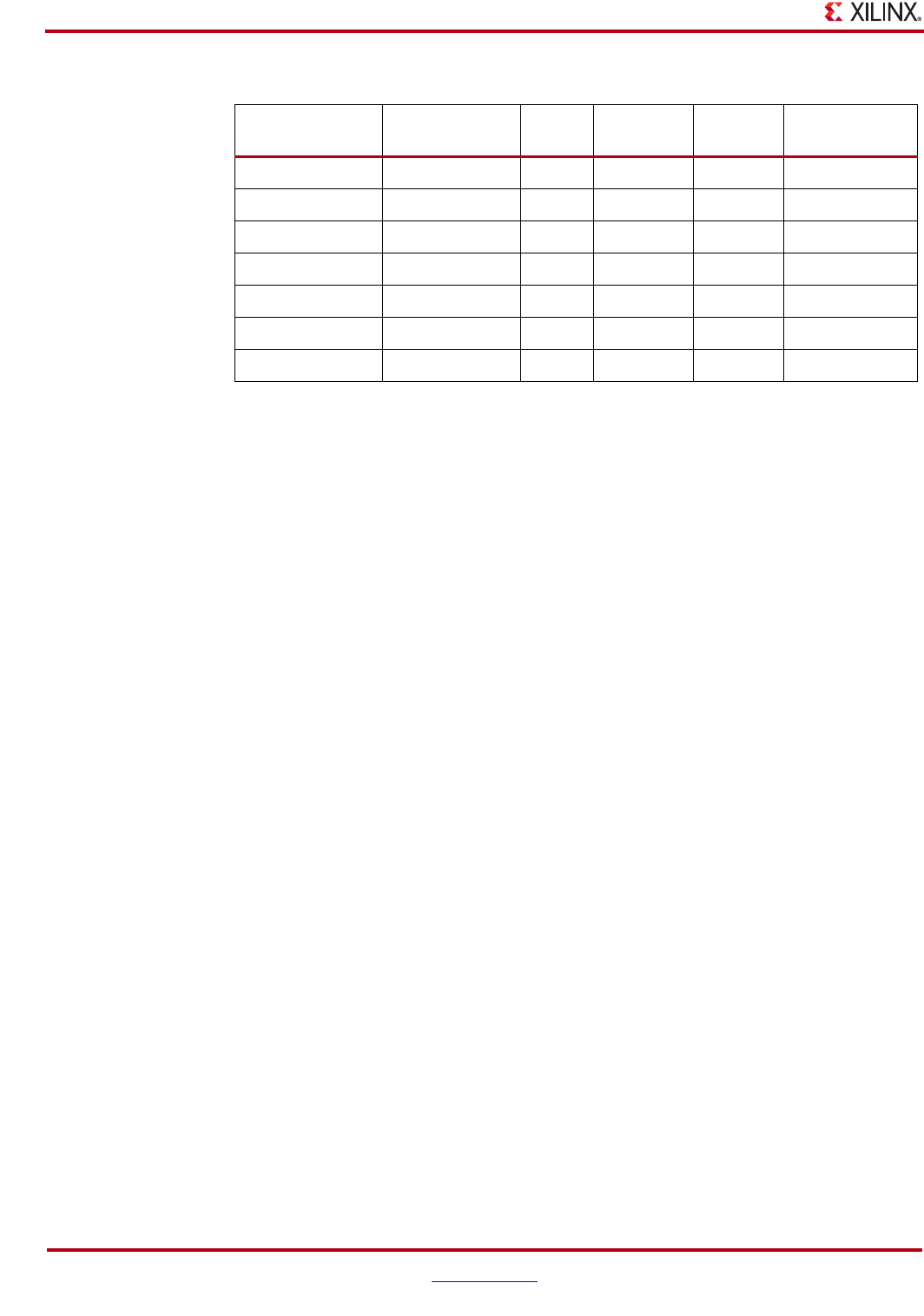
62 www.xilinx.com ML605 Hardware User Guide
UG534 (v1.2.1) January 21, 2010
Chapter 1: ML605 Evaluation Board
Table 1-29: Power Supply Voltages for HPC Connector
Voltage Supply Allowable
Voltage Range No Pins Max Amps Tolerance Max Capacitive
Load
VADJ Fixed 2.5V 4 4 +/- 5% 1000 uF
VIO_B_M2C 0-VADJ 2 1.15 +/- 5% 500 uF
VREF_A_M2C 0-VADJ 1 1 mA +/- 2% 10 uF
VREF_B_M2C 0-VIO_B_M2C 1 1 mA +/- 2% 10 uF
3P3VAUX 3.3V 1 20 mA +/- 5% 150 uF
3P3V 3.3V 4 3 +/- 5% 1000 uF
12P0V 12V 2 1 +/- 5% 1000 uF

ML605 Hardware User Guide www.xilinx.com 63
UG534 (v1.2.1) January 21, 2010
Detailed Description
20. VITA 57.1 FMC LPC Connector
The ML605 implements both the High Pin Count (HPC, J64) and Low Pin Count (LPC, J63)
connector options of VITA 57.1.1 FMC specification. This section discusses the FMC LPC
J63 connector.
The FMC standard calls for two connector densities: a High Pin Count (HPC) and a Low
Pin Count (LPC) implementation. A common 10 x 40 position (400 pin locations) connector
form factor is used for both versions. The HPC version is fully populated with 400 pins
present, and the LPC version is partially populated with 160 pins.
The 10 x 40 rows of a FMC LPC connector provides connectivity for:
•68 single-ended or 34 differential user defined signals
•1 MGT
•1 MGT clock
•2 differential clocks
•61 ground, 10 power connections
Of the above signal and clock connectivity capability, the ML605 implements the full set:
•34 differential user-defined pairs:
♦34 LA pairs
•1 MGT
•1 MGT clock
•2 differential clocks
Signaling Speed Ratings:
•Single-ended: 9 GHz / 18 Gb/s
•Differential
♦Optimal Vertical: 9 GHz / 18 Gb/s
♦Optimal Horizontal: 16 GHz / 32 Gb/s
♦High Density Vertical 7 GHz / 15 Gb/s
Mechanical specifications:
•Samtec SEAM/SEAF Series
•1.27mm x 1.27mm (0.050" x 0.050") pitch
The Samtec connector system is rated for signaling speeds up to 9 GHz (18 Gb/s) based on
a -3 dB insertion loss point within a two-level signaling environment.
Note: The ML605 board VADJ voltage for the FMC HPC and LPC connectors (J64 and J63) is fixed
at 2.5V (non-adjustable). The 2.5V rail cannot be turned off. The ML605 VITA 57.1 FMC interfaces
are compatible with 2.5V mezzanine cards capable of supporting 2.5V VADJ.
64 www.xilinx.com ML605 Hardware User Guide
UG534 (v1.2.1) January 21, 2010
Chapter 1: ML605 Evaluation Board
Table 1-30 shows the VITA 57.1 FMC LPC connections. The connector pinout is in
Appendix B, “VITA 57.1 FMC LPC (J63) and HPC (J64) Connector Pinout.”
Any signal named FMC_LPC_xxxx that is wired between a U1 FPGA pin and some other
device does not appear in this table..
Table 1-30: VITA 57.1 FMC LPC Connections
J63 FMC
LPC Pin Schematic Net Name U1 FPGA
Pin
J63 FMC
LPC Pin Schematic Net Name U1 FPGA
Pin
C2 FMC_LPC_DP0_C2M_P D1 D4 FMC_LPC_GBTCLK0_M2C_P M6
C3 FMC_LPC_DP0_C2M_N D2 D5 FMC_LPC_GBTCLK0_M2C_N M5
C6 FMC_LPC_DP0_M2C_P G3 D8 FMC_LPC_LA01_CC_P F31
C7 FMC_LPC_DP0_M2C_N G4 D9 FMC_LPC_LA01_CC_N E31
C10 FMC_LPC_LA06_P K33 D11 FMC_LPC_LA05_P H34
C11 FMC_LPC_LA06_N J34 D12 FMC_LPC_LA05_N H33
C14 FMC_LPC_LA10_P F30 D14 FMC_LPC_LA09_P L25
C15 FMC_LPC_LA10_N G30 D15 FMC_LPC_LA09_N L26
C18 FMC_LPC_LA14_P C33 D17 FMC_LPC_LA13_P D34
C19 FMC_LPC_LA14_N B34 D18 FMC_LPC_LA13_N C34
C22 FMC_LPC_LA18_CC_P L29 D20 FMC_LPC_LA17_CC_P N28
C23 FMC_LPC_LA18_CC_N L30 D21 FMC_LPC_LA17_CC_N N29
C26 FMC_LPC_LA27_P R31 D23 FMC_LPC_LA23_P R28
C27 FMC_LPC_LA27_N R32 D24 FMC_LPC_LA23_N R27
D26 FMC_LPC_LA26_P L33
D27 FMC_LPC_LA26_N M32
G2 FMC_LPC_CLK1_M2C_P F33 H2 FMC_LPC_PRSNT_M2C_L AD9
G3 FMC_LPC_CLK1_M2C_N G33 H4 FMC_LPC_CLK0_M2C_P A10
G6 FMC_LPC_LA00_CC_P K26 H5 FMC_LPC_CLK0_M2C_N B10
G7 FMC_LPC_LA00_CC_N K27 H7 FMC_LPC_LA02_P G31
G9 FMC_LPC_LA03_P J31 H8 FMC_LPC_LA02_N H30
G10 FMC_LPC_LA03_N J32 H10 FMC_LPC_LA04_P K28
G12 FMC_LPC_LA08_P J30 H11 FMC_LPC_LA04_N J29
G13 FMC_LPC_LA08_N K29 H13 FMC_LPC_LA07_P G32
G15 FMC_LPC_LA12_P E32 H14 FMC_LPC_LA07_N H32
G16 FMC_LPC_LA12_N E33 H16 FMC_LPC_LA11_P D31
G18 FMC_LPC_LA16_P A33 H17 FMC_LPC_LA11_N D32
G19 FMC_LPC_LA16_N B33 H19 FMC_LPC_LA15_P C32
ML605 Hardware User Guide www.xilinx.com 65
UG534 (v1.2.1) January 21, 2010
Detailed Description
References
See the data sheet for the ROHS compliant FMC HPC Samtec SEARAY connector (carrier
side socket ASP-134486-01; module side plug ASP-134488-01), and the high-speed
characterization report for this connector system on the Samtec website. [Ref 32]
21. Power Management
AC Adapter and Input Power Jack/Switch
The ML605 is powered from a 12V source that is connected through a 6-pin (2X3) right-
angle Mini-Fit type connector J60. The AC-to-DC power supply included in the kit has a
mating 6-pin plug.
When the ML605 is installed into a table top or tower PC's PCIe slot, the ML605 is typically
powered from the PC ATX power supply. One of the ATX hard disk type 4-pin power
connectors is plugged into ML605 connector J25. The ML605 can be powered with the AC
power adapter even when plugged into a PC PCIe motherboard slot; however, users are
cautioned not to also connect an ATX 4-pin power connector to J25. See the caution notes
below and in Figure 1-23, page 53.
Caution! DO NOT plug a PC ATX power supply 6-pin connector into ML605 connector J60.
The ATX 6-pin connector has a different pinout than ML605 J60, and connecting the ATX 6-pin
connector will damage the ML605 and void the board warranty.
Caution! DO NOT apply power to J60 and the 4-pin ATX disk drive connector J25 at the same
time as this will damage the ML605 board. Refer to Figure 1-23, page 53 for details.
The ML605 power can be turned on or off through the board mounted slide switch SW2.
When the switch is in the on position, a green LED (DS25) is illuminated.
G21 FMC_LPC_LA20_P P29 H20 FMC_LPC_LA15_N B32
G22 FMC_LPC_LA20_N R29 H22 FMC_LPC_LA19_P M30
G24 FMC_LPC_LA22_P N27 H23 FMC_LPC_LA19_N N30
G25 FMC_LPC_LA22_N P27 H25 FMC_LPC_LA21_P R26
G27 FMC_LPC_LA25_P P31 H26 FMC_LPC_LA21_N T26
G28 FMC_LPC_LA25_N P30 H28 FMC_LPC_LA24_P N32
G30 FMC_LPC_LA29_P N34 H29 FMC_LPC_LA24_N P32
G31 FMC_LPC_LA29_N P34 H31 FMC_LPC_LA28_P N33
G33 FMC_LPC_LA31_P M31 H32 FMC_LPC_LA28_N M33
G34 FMC_LPC_LA31_N L31 H34 FMC_LPC_LA30_P M26
G36 FMC_LPC_LA33_P K32 H35 FMC_LPC_LA30_N M27
G37 FMC_LPC_LA33_N K31 H37 FMC_LPC_LA32_P N25
H38 FMC_LPC_LA32_N M25
Table 1-30: VITA 57.1 FMC LPC Connections (Cont’d)
J63 FMC
LPC Pin Schematic Net Name U1 FPGA
Pin
J63 FMC
LPC Pin Schematic Net Name U1 FPGA
Pin
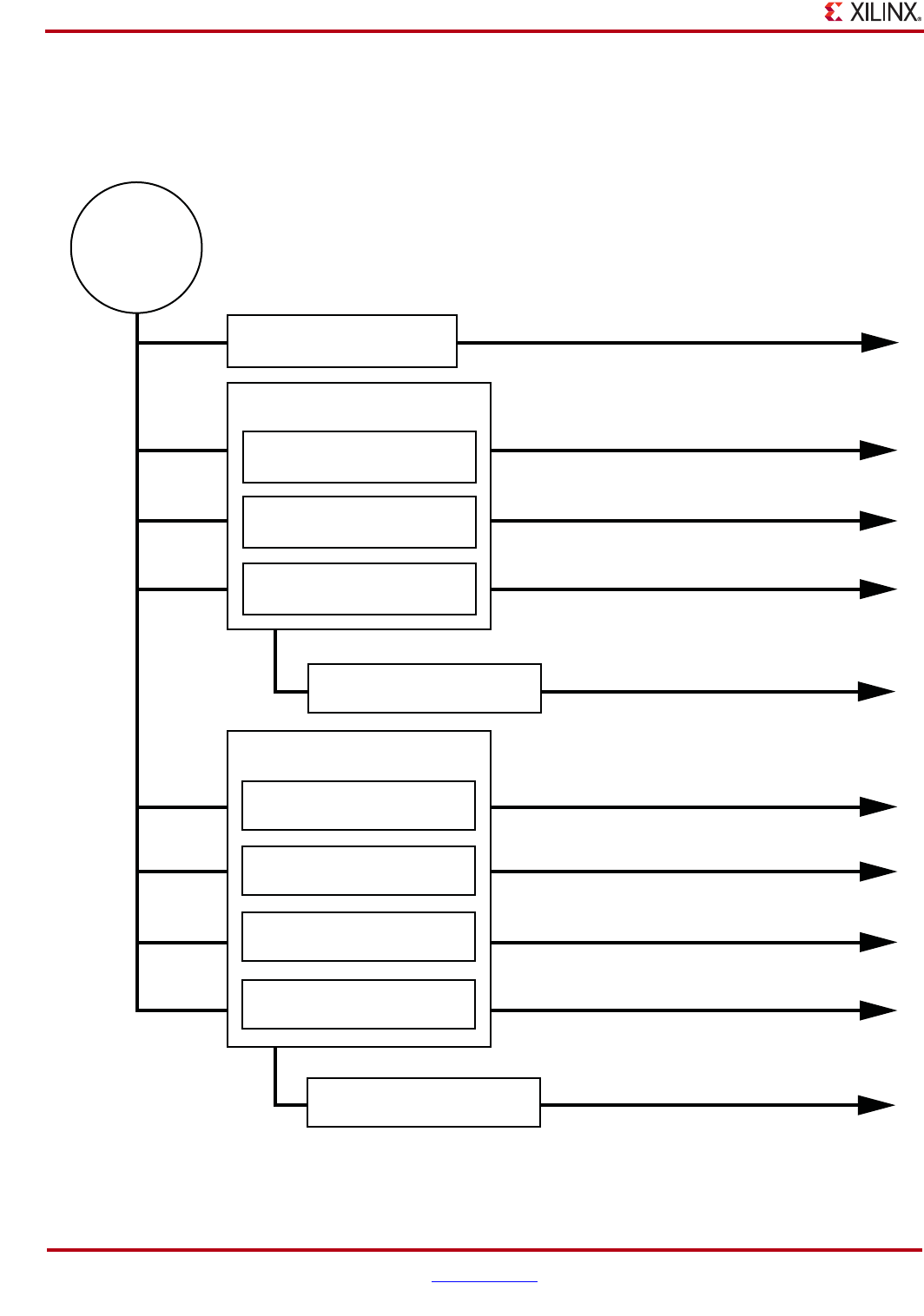
66 www.xilinx.com ML605 Hardware User Guide
UG534 (v1.2.1) January 21, 2010
Chapter 1: ML605 Evaluation Board
Onboard Power Regulation
Figure 1-28 shows the ML605 onboard power supply architecture. The ML605 uses power
solutions from Texas Instruments.
X-Ref Target - Figure 1-28
Figure 1-28: ML605 Onboard Power Regulators
Linear Regulator TL1963
5.0V@1.5A max U8
Linear Regulator TL1963A
1.8V@500mA max U79
Power Controller 2
UCD9240PFC U25
Switching Regulator UCD7230RG
1.00V@6A max U35
Switching Regulator UCD7230RG
1.20V@6A max U36
Switching Module PTD08A010W
1.5V@10A max U20
Switching Module PTD08A010W
3.3V@10A max U21
Linear Regulator TPS51200
0.75V@3A max U17
Sink/Source DDR Regulator
Power Supply
VCC5
VCCINT
VCCAUX
VCC1V8
MGT_AVCC
MGT_AVTT
VCC3V3
VTTDDR
VCC2V5, FPGA_VCC2V5
VCC1V5, FPGA_VCC1V5
12V
PWR Jack
J25/J60
Power Controller 1
UCD9240PFC U24
Switching Module PTD08A020W
1.00V@20A max U42
Switching Module PTD08A010W
2.50V@10A max U91
Switching Module PTD08A020W
2.5V@20A max U43
UG534_28_012010
ML605 Hardware User Guide www.xilinx.com 67
UG534 (v1.2.1) January 21, 2010
Detailed Description
Voltage and current monitoring and control are available for selected power rails through
Texas Instruments’ Fusion Digital Power™ graphical user interface (GUI). Both onboard
TI power controllers are wired to the same PMBus. The PMBus connector, J3, is provided
for use with the TI USB Interface Adapter PMBus pod and associated TI GUI.
References
For more detailed information about this technology and the various power management
controllers and regulator modules offered by Texas Instruments, visit
http://www.ti.com/ww/en/analog/digital-power/index.html.
Table 1-31: Onboard Power System Devices
Device Type Reference
Designator Description Power Rail
Net Name
Power Rail
Voltage
Schematic
Page
UCD9240PFC U24 PMBus Controller - Core (Addr = 52) 35
PTD08A020W U42 20A 0.6V - 3.6V Adj. Switching Regulator VCCINT_FPGA 1.00V 36
PTD08A020W U43 20A 0.6V - 3.6V Adj. Switching Regulator VCC2V5_FPGA 2.50V 37
PTD08A010W U91 10A 0.6V - 3.6V Adj. Switching Regulator VCCAUX 2.50V 38
UCD9240PFC U25 PMBus Controller - Aux (Addr = 53) 40
UCD7230RGWR U35 6A 0.6V - 3.6V Adj. Switching Regulator MGT_AVCC 1.00V 41
UCD7230RGWR U36 6A 0.6V - 3.6V Adj. Switching Regulator MGT_AVTT 1.20V 42
PTD08A010W U20 10A 0.6V - 3.6V Adj. Switching Regulator VCC_1V5 1.50V 43
PTD08A010W U21 10A 0.6V - 3.6V Adj. Switching Regulator VCC_3V3 3.30V 44
TPS79518DCQR U79 500mA Fixed Linear Regulator VCC_1V8 1.80V 45
TPS512300DRCT U17 3A DDR3 VTERM Tracking Linear
Regulator
VTTDDR 0.75V 45
TPS512300DRCT U17 10mA Tracking Reference output VTTVREF 0.75V 45
TL1963 U8 1.5A Fixed Linear Regulator VCC5 5.00V 35
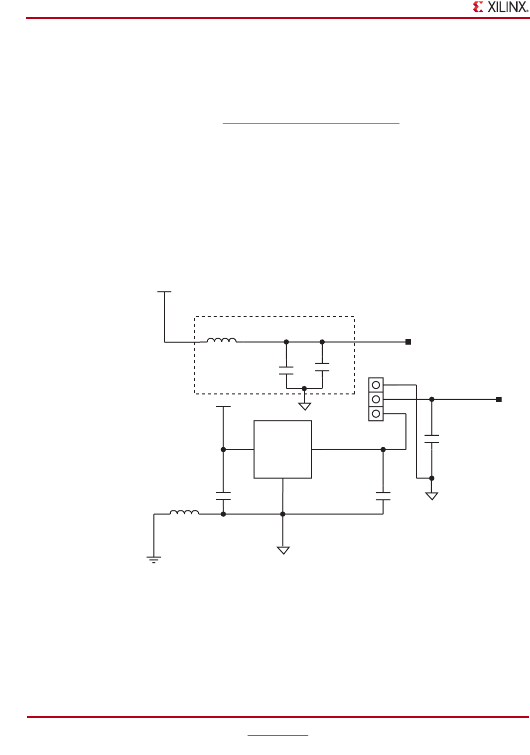
68 www.xilinx.com ML605 Hardware User Guide
UG534 (v1.2.1) January 21, 2010
Chapter 1: ML605 Evaluation Board
22. System Monitor
The System Monitor provides information regarding the FPGA on-chip temperature and
power supply conditions via JTAG and an internal FPGA interface. The System Monitor
can also be used to monitor external analog signals via 17 external analog input channels.
For more information regarding this functionality, which is featured on every Virtex-6
family member, see http://www.xilinx.com/systemmonitor.
This section provides a brief overview of the System Monitor related functionality that is
supported on the ML605.
Reference and Power Supply
The System Monitor has dedicated analog power supply pins and supports the use of an
external 1.25V reference IC (U23) for the analog-to-digital conversion process. An option
(using jumper J19) to select an on-chip reference is also provided; however, the highest
accuracy over a temperature range of -40°C to +125°C is obtained using an external
reference. Figure 1-29 illustrates the power supply and reference options on the ML605.
For a more detailed discussion of these requirements, see the Virtex-6 FPGA System Monitor
User Guide. [Ref 15]
X-Ref Target - Figure 1-29
Figure 1-29: System Monitor External Reference
VCC5
VCC2V5
IN OUT
GND
REF3012
Jumper on pins 1-2
Default Setting:
1-2 Select External Reference
2-3 Select On-Chip Reference
SYSMON_AVDD
Analog Supply Filter
Ferrie Bead
12
3
U23
REF3012AIDBZT X5R
10V
0.1UF
C383
X5R
10V
0.1UF
C78
C79
0.1UF
10V
X5R
X5R
6.3V
1UF
C191
C190
1UF
6.3V
X5R
1
2
1.25V
AGND
AGND
GND
SYSMON_VREFP
1
2
3
J19
AGND
UG534_29_081209
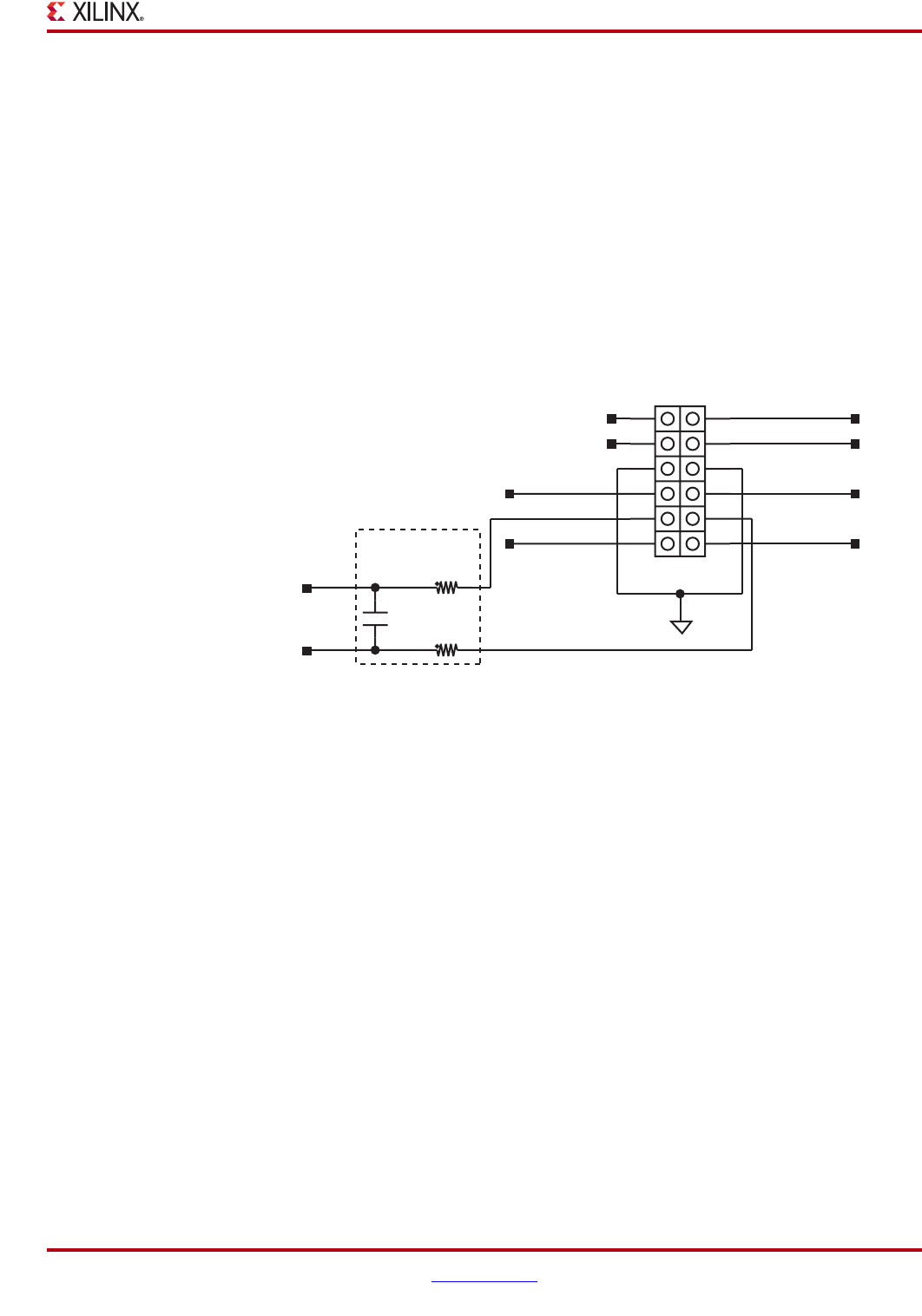
ML605 Hardware User Guide www.xilinx.com 69
UG534 (v1.2.1) January 21, 2010
Detailed Description
System Monitor Header (J35)
Figure 1-30 shows the pinout for the System Monitor 12-pin header. The header provides
user access to the analog power supply (AVdd) and the 1.25V reference shown in
Figure 1-29, page 68. Access to the FPGA thermal diode and dedicated analog input
channel (Vp/Vn) is also provided on this header. The header can be used to connect user
specific analog signals and sensors to the system monitor.
The kelvin points for a 5 milliohm current sensing shunt in the FPGA 1V Vccint core supply
are also available on this header. By connecting header pins 9 to 11 and 10 to 12 using
jumpers, the system monitor can be used to monitor the FPGA core current and power
consumption. This can be used to collect useful power information about a particular
design or implementation.
X-Ref Target - Figure 1-30
Figure 1-30: System Monitor Header (J35)
System Monitor
Header
Dedicated Analog Inputs
FPGA
Thermal Diode
access
To Measure VCCINT Current:
Jumper on 9-11, 10-12
Connect Vccint shunt to Vp,Vn
Vccint_shunt_N Vccint_shunt_P
C169
0.01UF
16V
X7R
FPGA_DX_N
FPGA_DX_P
NC
NC
SYSMON_AVDD
1.25V Reference
12
3
56
78
910
4
1211
J35
SYSMON_VP
SYSMON_VN
R232
100
1/16W
1%1%
1/16W
100
R233
AGND
Anti-alias Filter
UG534_37 _081209
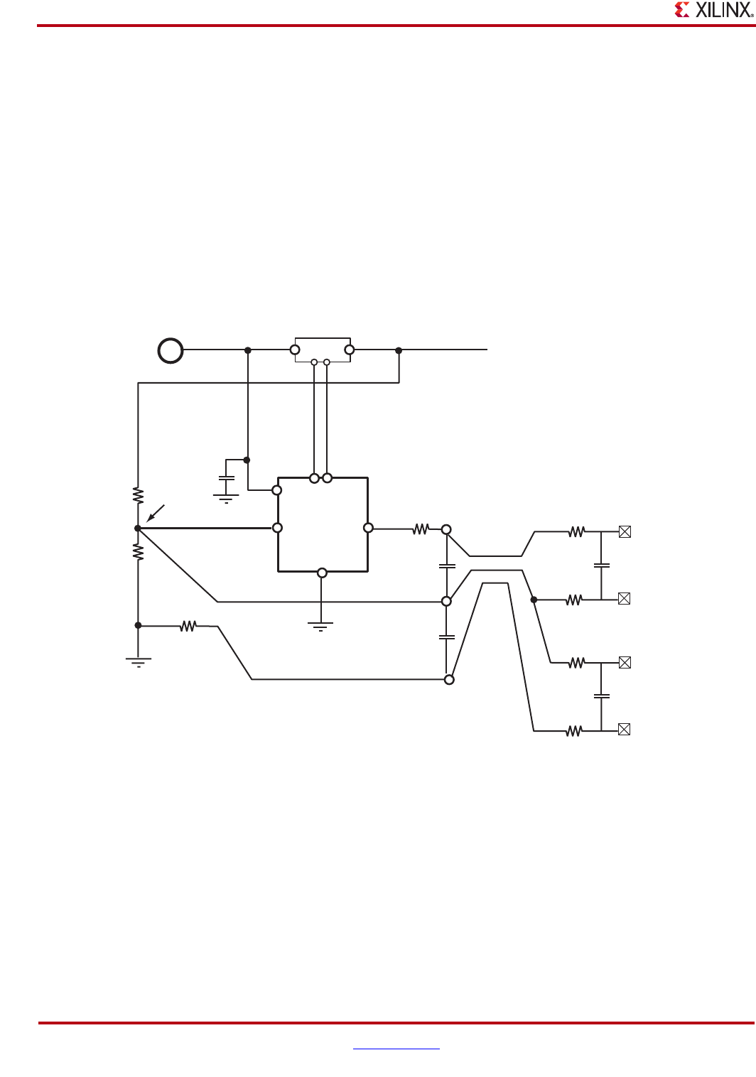
70 www.xilinx.com ML605 Hardware User Guide
UG534 (v1.2.1) January 21, 2010
Chapter 1: ML605 Evaluation Board
ML605 Board Power Monitor
In addition to monitoring the FPGA core supply power consumption, two auxiliary analog
input channels (of the 16 that are available) are used to implement a power monitor for the
entire ML605 board. The board power is monitored at the 12V power input connector.
Figure 1-31 shows how the power monitor is implemented and connected to the System
Monitor auxiliary input channels 12 and 13. A simple resistor divider is used to monitor
the 12V supply voltage and to provide a reference voltage to an instrumentation amplifier
(InAmp). The voltage on the auxiliary channel 12 is equal to supply voltage divided by 24
(~ 0.5V).
The InAmp is used to amplify (by a factor of 50) the voltage dropped across a 2 milliohm
current sense shunt. The voltage at the output of the InAmp is proportional to the current.
The voltage on auxiliary channel 13 = Current (amps) x 0.002 x 50. (e.g., 5A = 0.5V).
X-Ref Target - Figure 1-31
Figure 1-31: ML605 12V Power Monitor
12V Supply Monitor
11.5kΩ ±0.5%
499Ω ±0.5%
~470Ω
~470Ω
10nF
1kΩ
1kΩ
VAUXP[13]
Current Channel
Voltage Channel
VAUXN[13]
INA213
GND
OUT
REF
R1 R2
IN+ IN-
V+
2mΩ ±1%
SC70-6
Package
50V/V
~0.5V
10nF
1kΩ
1kΩ
VAUXP[12]
VAUXN[12]
K1 K2
100nF
10nF
10nF
UG534_38 _081209
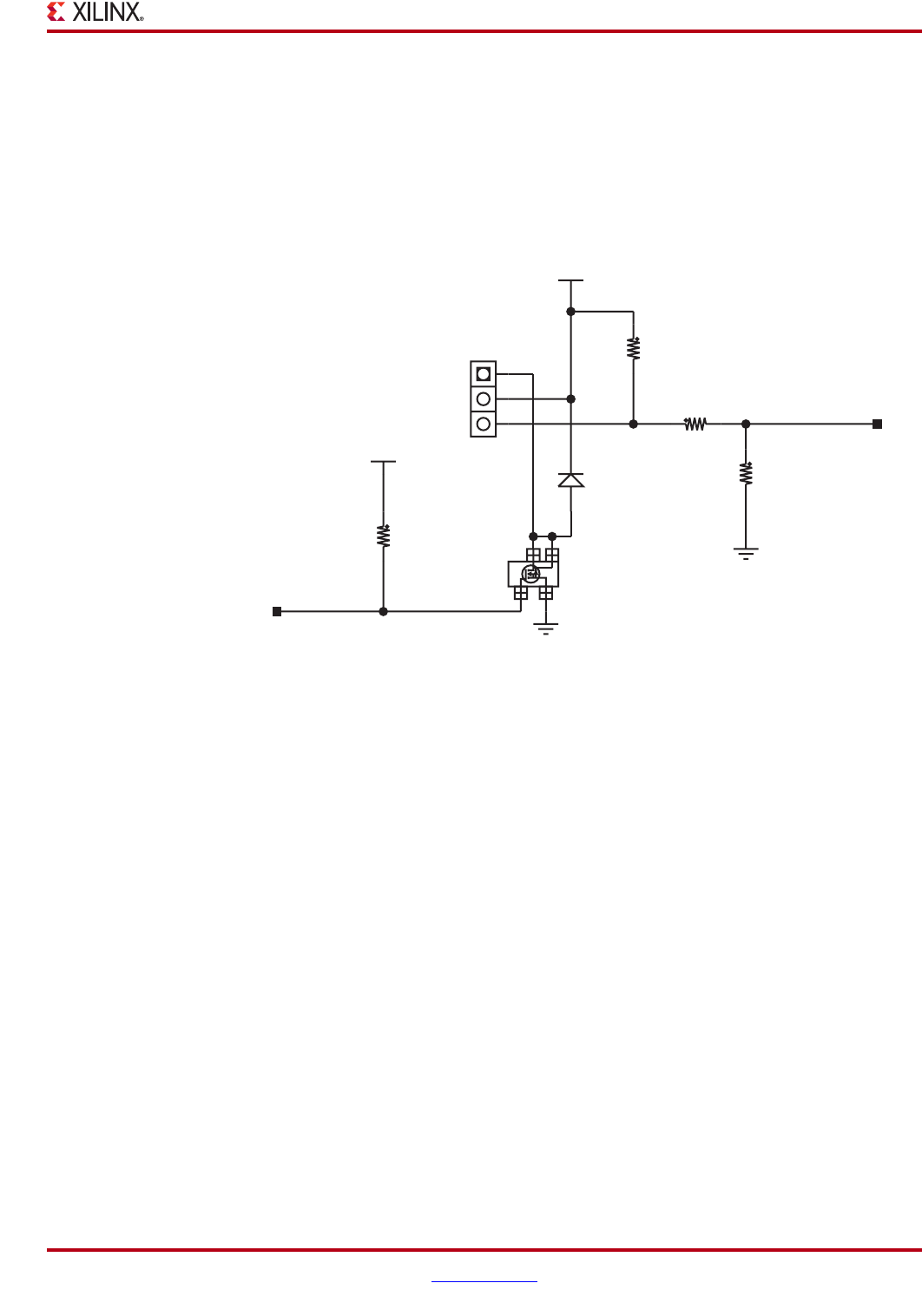
ML605 Hardware User Guide www.xilinx.com 71
UG534 (v1.2.1) January 21, 2010
Detailed Description
Fan Controller
In highly demanding situations, active thermal management in the form of a heat sink and
fan may be required. In order to support this, drive circuitry for an external fan has been
provided on the ML605. A fan with tach output can be connect at header J59 as shown in
Figure 1-32. The fan PWM signal is generated by the FPGA and the tach input can be used
to close the control loop and regulate the fan speed. Alternatively, the FPGA temperature
as recorded by the System Monitor can be used to close the PWM control loop for the fan.
X-Ref Target - Figure 1-32
Figure 1-32: ML605 Fan Driver
0
VCC12_P
VCC2V5
1
2
3
J59
21
D16
1N4148
R367
10.0K
1/16W
1%
1
4
3
2
Q24 NDT3055L
1%
1/16W
10.0K
R368
1%
4.75K
R358
12V
GND
Tach
1%
1/16W
10.0K
R369
SM_FAN_PWM
SM_FAN_TACH
UG534_39 _081209
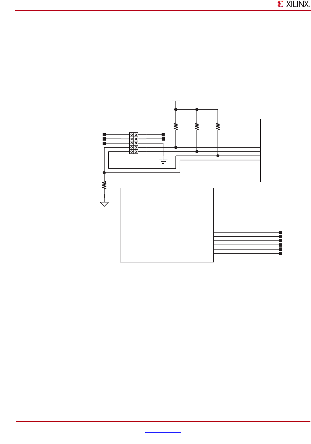
72 www.xilinx.com ML605 Hardware User Guide
UG534 (v1.2.1) January 21, 2010
Chapter 1: ML605 Evaluation Board
FPGA Power Supply Margining
The PMBus (IIC), which provides access to the 2 x UDC9240 power controllers, can also be
accessed via FPGA I/O in addition to a dedicated header (J3), see Figure 1-33. A full
description of the UDC9240 functionality is outside the scope of this user guide. However,
this useful feature can be used, for example, to margin the FPGA and board power
supplies when evaluating a design. The System Monitor provides accurate measurements
of the on-chip supply voltages as the FPGA supplies are margined. The PMBus (and fan)
connections are shown in Figure 1-33.
System Monitor ML605 Demonstration Design
The various features described in this section are easily evaluated using a MicroBlaze™
based reference designed provided with the ML605 Evaluation Board. This reference
design supports a UART based interface using a terminal program such as Hyperterminal
to provide information on the FPGA power supplies, temperature, and power
consumption. In addition, the UART interface can be used to margin the FPGA supplies
over the PMBus.
The System Monitor functionality can also be accessed at any time via JTAG using the
ChipScope Pro Analyzer tool without design modifications or cores inserted into a user
design. The ChipScope Pro Analyzer tool automatically connects to the System Monitor
via a JTAG cable after a connection is established.
References
For more information on using the System Monitor and an overview of the tool support for
this feature, see the Virtex-6 FPGA System Monitor User Guide. [Ref 15]
X-Ref Target - Figure 1-33
Figure 1-33: UDC9240 PMBus Access
9240
DGND1
AGND1
PMBus Connector
35
19
36
209
7
12
3
56
4
8
10
J3
PMBUS_DATA
PMBUS_ALERT
R301
100K
5% 5%
100K
R299 R300
100K
5%
PMBUS_CLK
PMBUS_CTRL
R335
1.0M
5%
TI_V3P3
UDC9240
NC
NC
NC
NC NC
IO_L9P_MRCC_34_L10
IO_L9N_MRCC_34_M10
IO_L10P_MRCC_34_AC10
IO_L10N_MRCC_34_AB10
IO_L11P_SRCC_34_AH9
IO_L11N_SRCC_34_AJ9
6vlx240tff1156
BANK 34
L10
M10
AC10
AB10
AH9
AJ9 PMBUS_CTRL_LS
SM_FAN_PWM
SM_FAN_TACH
PMBUS_ALERT_LS
PMBUS_CLK_LS
PMBUS_DATA_LS
UG534_35_081209
ML605 Hardware User Guide www.xilinx.com 73
UG534 (v1.2.1) January 21, 2010
Configuration Options
Configuration Options
The FPGA on the ML605 Evaluation Board can be configured by the following methods:
•“3. 128 Mb Platform Flash XL,” page 20
•“4. 32 MB Linear BPI Flash,” page 20
•“5. System ACE CF and CompactFlash Connector”
•“6. USB JTAG,” page 26
For more information, see the Virtex-6 FPGA Configuration User Guide at
http://www.xilinx.com/support/documentation/user_guides/ug360.pdf.
With the mode set to JTAG 101, the ML605 will not attempt to boot or load a bitstream
from either of the Flash devices. If a CompactFlash (CF) card is installed in the CF socket
U73, System ACE CF will attempt to load a bitstream from the CF card image address
pointed to by the image select switch S1. With no CF card present, the ML605 can be
configured via the onboard JTAG controller and USB download cable as described above.
With the mode set to either Slave SelectMAP 110, or BPI Mode 010, the FPGA will attempt
to configure itself from the selected Flash device as described in “3. 128 Mb Platform Flash
XL,” page 20.
Note: S1 switch 4 is the System ACE controller enable switch. When ON, this switch allows the
System ACE to boot at power-on if it finds a CF card present. In order to boot from BPI Flash U4 or
Xilinx Platform Flash (U27) without System ACE contention, S1 switch 4 must be OFF.
Table 1-32: Mode Switch S2 Settings
Mode Pins (M2,M1,M0) Configuration Mode
110 Slave SelectMAP
010 BPI Mode
101 JTAG

ML605 Hardware User Guide www.xilinx.com 75
UG534 (v1.2.1) January 21, 2010
Appendix A
Default Switch and Jumper Settings
Tabl e A -1: Default Switch Settings
REFDES Function/Type Default
SW2 Board power slide-switch off
SW1
User GPIO 8-pole DIP switch
8 off
7 off
6 off
5 off
4 off
3 off
2 off
1 off
S1
System ACE CF configuration and image select 4-pole DIP switch
4 SysACE Mode = 1(1) off
3SysAce CFGAddr 2 = 0 off
2SysAce CFGAddr 1 = 0 off
1 SysAce CFGAddr 0 = 0 off
S2
FPGA mode, boot PROM select and FPGA CCLK select 6-pole DIP
switch
6 FLASH_A23 = 0 off
5M2 = 0 off
4M1 = 1
M[2:0] = 010 = Master BPI-Up on
3M0 = 0 off
2 CS_SEL = 1 = boot from BPI Flash on
1 EXT_CCLK = 0 off
Notes:
1. S1 position 4 is the System ACE controller enable switch. When ON, this switch allows the System
ACE to boot at power on if it finds a CF card present. In order to boot from BPI Flash or Xilinx Platform
Flash without System ACE contention, S1 switch 4 must be OFF.
76 www.xilinx.com ML605 Hardware User Guide
UG534 (v1.2.1) January 21, 2010
Appendix A: Default Switch and Jumper Settings
Tabl e A -2: Default Jumper Settings
Jumper REFDES Function Default
J69 System ACE CF Error LED Enable Jump 1-2
GMII:
J66 pins 1-2: GMII/MII to Cu
pins 2-3: SGMII to Cu, no clk Jump 1 - 2
J67 pins 1-2: GMII/MII to Cu
pins 2-3: SGMII to Cu, no clk Jump 1 - 2
J68 J66 pins 1-2, J68 ON: RGMII, modified MII in Cu no jumper
FMC Bypass:
J18 exclude FMC LPC connector Jump 1 - 2
J17 exclude FMC LPC connector Jump 1 - 2
System Monitor:
J19 Test_mon_vrefp sourced by U23, REF3012 Jump 1 - 2
J35 measure voltage on R-kelvin on 12V rail Jump 9 - 11,
Jump 10 - 12
SFP Module:
J54 Full BW Jump 1 - 2
J65 SFP Enable Jump 1 - 2
PCIe Lane Size:
J42 1 lane Jump 1 - 2
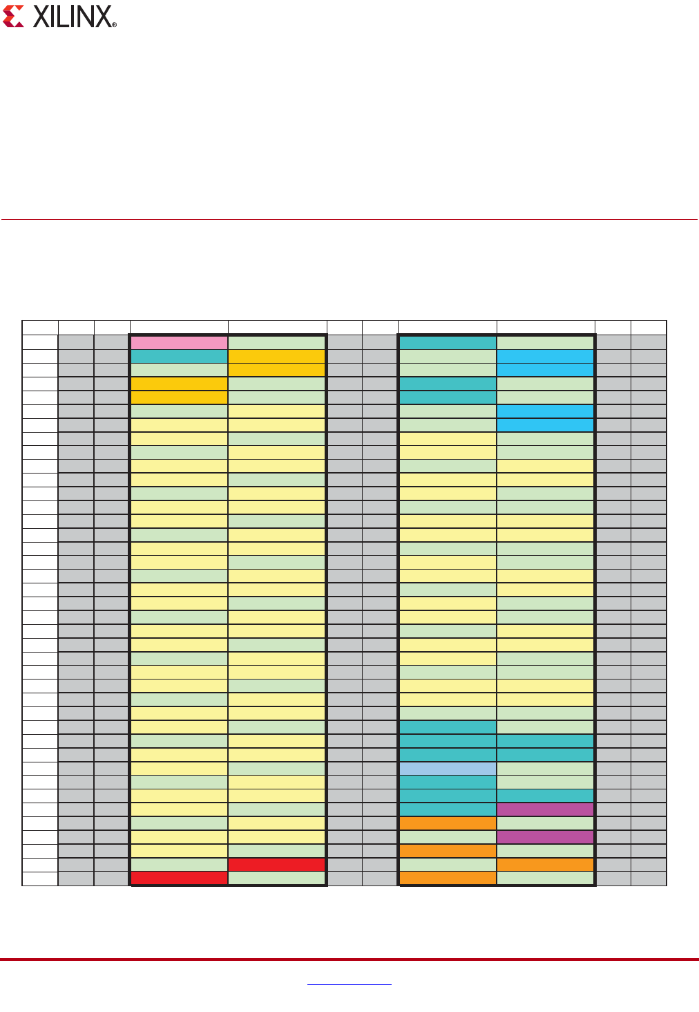
ML605 Hardware User Guide www.xilinx.com 77
UG534 (v1.2.1) January 21, 2010
Appendix B
VITA 57.1 FMC LPC (J63) and HPC (J64)
Connector Pinout
Figure B-1 shows the pinout of the FMC LPC connector. Pins marked NC are not
connected.
X-Ref Target - Figure B-1
Figure B-1: FMC LPC Connector Pinout
KJ H G FE D C BA
1 NC NC VR EF_A_M2C GND NC NC P G_C2M G ND NC NC
2 NC NC PR SNT_M2C_L CLK1_M2C_P NC NC GND DP0_C2M_P NC NC
3 NC NC GND C LK1_M2C_N NC NC GND DP0_C2M_N NC NC
4 NC NC CLK0_M2C_P GND NC NC GBTCLK0_M2C_P GND NC NC
5 NC NC CLK0_M2C_N GND NC NC GBTCLK0_M2C_N GND NC NC
6 NC NC GND LA00_P_CC NC NC GND DP0_M2C_P NC NC
7 NC NC LA02_P LA00_N_CC NC NC GND DP0_M2C_N NC NC
8 NC NC LA02_N GND NC NC LA01_P_CC GND NC NC
9 NCNC GND LA03_P NCNC LA01_N_CC GND NCNC
10 NC NC LA04_P LA03_N NC NC GND LA06_P NC NC
11 NC NC LA04_N GND NC NC LA05_P LA06_N NC NC
12 NC NC GND LA08_P NC NC LA05_N GND NC NC
13 NC NC LA07_P LA08_N NC NC GND GND NC NC
14 NC NC LA07_N GND NC NC LA09_P LA10_P NC NC
15 NC NC GND LA12_P NC NC LA09_N LA10_N NC NC
16 NC NC LA11_P LA12_N NC NC GND GND NC NC
17 NC NC LA11_N GND NC NC LA13_P GND NC NC
18 NC NC GND LA16_P NC NC LA13_N LA14_P NC NC
19 NC NC LA15_P LA16_N NC NC GND LA14_N NC NC
20 NC NC LA15_N GND NC NC LA17_P_CC GND NC NC
21 NC NC GND LA20_P NC NC LA17_N_CC GND NC NC
22 NC NC LA19_P LA20_N NC NC GND LA18_P _CC NC NC
23 NC NC LA19_N GND NC NC LA23_P LA18_N_CC NC NC
24 NC NC GND LA22_P NC NC LA23_N GND NC NC
25 NC NC LA21_P LA22_N NC NC GND GND NC NC
26 NC NC LA21_N GND NC NC LA26_P LA27_P NC NC
27 NC NC GND LA25_P NC NC LA26_N LA27_N NC NC
28 NC NC LA24_P LA25_N NC NC GND GND NC NC
29 NC NC LA24_N GND NC NC TCK GND NC NC
30 NC NC GND LA29_P NC NC TDI S CL NC NC
31 NC NC LA28_P LA29_N NC NC TDO S DA NC NC
32 NC NC LA28_N GND NC NC 3P3VAUX GND NC NC
33 NC NC GND LA31_P NC NC TMS GND NC NC
34 NC NC LA30_P LA31_N NC NC TR ST_L GA0 NC NC
35 NC NC LA30_N GND NC NC GA1 12P0V NC NC
36 NC NC GND LA33_P NC NC 3P3V GND NC NC
37 NC NC LA32_P LA33_N NC NC GND 12P0V NC NC
38 NC NC LA32_N GND NC NC 3P3V GND NC NC
39 NC NC GND VADJ NC NC GND 3P3V NC NC
40 NC NC VADJ GND NC NC 3P3V GND NC NC
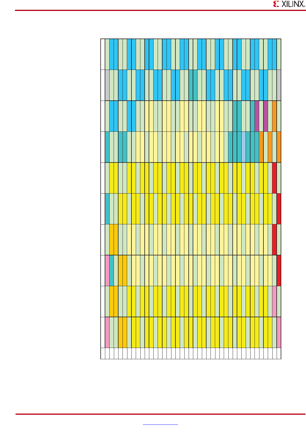
78 www.xilinx.com ML605 Hardware User Guide
UG534 (v1.2.1) January 21, 2010
Appendix B: VITA 57.1 FMC LPC (J63) and HPC (J64) Connector Pinout
Figure B-2 shows the pinout of the FMC HPC connector.
X-Ref Target - Figure B-2
Figure B-2: FMC HPC Connector Pinout
KJHGFEDCBA
1 VREF_B_M2C GND VREF_A_M2C GND PG_M2C GND PG_C2M GND RES1 GND
2 GND CLK3_M2C_P PRS NT_M2C _L CLK1_M2C_P GND HA01_P_CC G ND DP0_C2M_P GND DP1_M2C_P
3 GND C LK3_M2C_N GND CLK1_M2C_N GND HA01_N_C C GND DP0_C2M_N GND DP 1_M2C_N
4 CLK2_M2C_P GND C LK0_M2C_P GND HA00_P_C C GND GBTC LK 0_M2C_P GND DP9_M2C_P GND
5 CLK2_M2C_N GND C LK 0_M2C_N GND HA00_N_CC GND GBTC LK0_M2C_N GND DP9_M2C_N G ND
6 GND HA03_P GND LA00_P _CC GND HA05_P GND DP0_M2C _P GND DP2_M2C_P
7 HA02_P HA03_N LA02_P LA00_N_CC HA04_P HA05_N GND DP0_M2C_N GND DP2_M2C_N
8 HA02_N GND LA02_N GND HA04_N GND LA01_P _CC GND DP8_M2C_P GND
9 GND HA07_P GND LA03_P GND HA09_P LA01_N_C C GND DP8_M2C_N G ND
10 HA06_P HA07_N LA04_P LA03_N HA08_P HA09_N GND LA06_P GND DP3_M2C_P
11 HA06_N GND LA04_N GND HA08_N GND LA05_P LA06_N GND DP3_M2C_N
12 GND HA11_P GND LA08_P GND HA13_P LA05_N GND DP7_M2C_P GND
13 HA10_P HA11_N LA07_P LA08_N HA12_P HA13_N GND GND DP7_M2C_N GND
14 HA10_N GND LA07_N GND HA12_N GND LA09_P LA10_P GND DP4_M2C _P
15 GND HA14_P GND LA12_P GND HA16_P LA09_N LA10_N GND DP4_M2C_N
16 HA17_P_C C HA14_N LA11_P LA12_N HA15_P HA16_N GND GND DP6_M2C_P GND
17 HA17_N_C C G ND LA11_N GND HA15_N GND LA13_P GND DP6_M2C_N GND
18 GND HA18_P GND LA16_P GND HA20_P LA13_N LA14_P GND DP5_M2C_P
19 HA21_P HA18_N LA15_P LA16_N HA19_P HA20_N GND LA14_N GND DP5_M2C_N
20 HA21_N GND LA15_N GND HA19_N GND LA17_P _CC GND GBTC LK1_M2C_P G ND
21 GND HA22_P GND LA20_P GND HB03_P LA17_N_C C GND GBTC LK1_M2C_N GND
22 HA23_P HA22_N LA19_P LA20_N HB02_P HB03_N GND LA18_P_CC GND DP1_C2M_P
23 HA23_N GND LA19_N GND HB02_N GND LA23_P LA18_N_C C GND DP1_C2M_N
24 GND HB01_P GND LA22_P GND HB05_P LA23_N GND DP9_C2M_P GND
25 HB00_P_C C HB01_N LA21_P LA22_N HB04_P HB05_N GND GND DP9_C2M_N G ND
26 HB00_N_C C G ND LA21_N GND HB04_N GND LA26_P LA27_P GND DP2_C2M_P
27 GND HB07_P GND LA25_P GND HB09_P LA26_N LA27_N GND DP2_C 2M_N
28 HB06_P_C C HB07_N LA24_P LA25_N HB08_P HB09_N GND GND DP8_C2M_P GND
29 HB06_N_C C G ND LA24_N GND HB08_N GND TCK GND DP8_C2M_N GND
30 GND HB11_P GND LA29_P GND HB13_P TDI S CL GND DP3_C2M_P
31 HB10_P HB11_N LA28_P LA29_N HB12_P HB13_N TDO S DA GND DP3_C2M_N
32 HB10_N GND LA28_N GND HB12_N GND 3P3VAUX GND DP7_C2M_P GND
33 GND HB15_P GND LA31_P GND HB19_P TMS GND DP7_C2M_N GND
34 HB14_P HB15_N LA30_P LA31_N HB16_P HB19_N TR ST_L GA0 GND DP 4_C2M_P
35 HB14_N GND LA30_N GND HB16_N GND GA1 12P0V GND DP4_C2M_N
36 GND HB18_P GND LA33_P GND HB21_P 3P 3V GND DP6_C2M_P GND
37 HB17_P_C C HB18_N LA32_P LA33_N HB20_P HB21_N GND 12P0V DP6_C2M_N GND
38 HB17_N_C C G ND LA32_N GND HB20_N GND 3P3V GND GND DP5_C 2M_P
39 GND VIO_B_M2C GND VADJ GND VADJ GND 3P3V GND DP5_C2M_N
40 V IO_B _M2C GND VADJ G ND VADJ GND 3P3V GND RE S0 GND
ML605 Hardware User Guide www.xilinx.com 79
UG534 (v1.2.1) January 21, 2010
Appendix C
ML605 Master UCF
The UCF template is provided for designs that target the ML605. Net names provided in
the constraints below correlate with net names on the ML605 Rev. D schematic. On
identifying the appropriate pins, the net names below should be replaced with net names
in the user RTL. See the Constraints Guide for more information.
Users can refer to the UCF files generated by tools such as MIG (Memory Interface
Generator for memory interfaces) and BSB (Base System Builder) for more detailed
information concerning the I/O standards required for each particular interface. The FMC
connectors J63 and J64 are connected to 2.5V Vcco banks. Because each user’s FMC card
implements customer-specific circuitry, the FMC bank I/O standards must be uniquely
defined by each customer.
NET "CLK_33MHZ_SYSACE" LOC = "AE16"; ## 93 on U19
NET "CPU_RESET" LOC = "H10"; ## 2 on SW10 pushbutton (active-High)
##
NET "DDR3_A0" LOC = "L14"; ## 98 on J1
NET "DDR3_A1" LOC = "A16"; ## 97 on J1
NET "DDR3_A2" LOC = "B16"; ## 96 on J1
NET "DDR3_A3" LOC = "E16"; ## 95 on J1
NET "DDR3_A4" LOC = "D16"; ## 92 on J1
NET "DDR3_A5" LOC = "J17"; ## 91 on J1
NET "DDR3_A6" LOC = "A15"; ## 90 on J1
NET "DDR3_A7" LOC = "B15"; ## 86 on J1
NET "DDR3_A8" LOC = "G15"; ## 89 on J1
NET "DDR3_A9" LOC = "F15"; ## 85 on J1
NET "DDR3_A10" LOC = "M16"; ## 107 on J1
NET "DDR3_A11" LOC = "M15"; ## 84 on J1
NET "DDR3_A12" LOC = "H15"; ## 83 on J1
NET "DDR3_A13" LOC = "J15"; ## 119 on J1
NET "DDR3_A14" LOC = "D15"; ## 80 on J1
NET "DDR3_A15" LOC = "C15"; ## 78 on J1
NET "DDR3_BA0" LOC = "K19"; ## 109 on J1
NET "DDR3_BA1" LOC = "J19"; ## 108 on J1
NET "DDR3_BA2" LOC = "L15"; ## 79 on J1
NET "DDR3_CAS_B" LOC = "C17"; ## 115 on J1
NET "DDR3_CKE0" LOC = "M18"; ## 73 on J1
NET "DDR3_CKE1" LOC = "M17"; ## 74 on J1
NET "DDR3_CLK0_N" LOC = "H18"; ## 103 on J1
NET "DDR3_CLK0_P" LOC = "G18"; ## 101 on J1
NET "DDR3_CLK1_N" LOC = "L16"; ## 104 on J1
NET "DDR3_CLK1_P" LOC = "K16"; ## 102 on J1
NET "DDR3_D0" LOC = "J11"; ## 5 on J1
NET "DDR3_D1" LOC = "E13"; ## 7 on J1
NET "DDR3_D2" LOC = "F13"; ## 15 on J1
NET "DDR3_D3" LOC = "K11"; ## 17 on J1
NET "DDR3_D4" LOC = "L11"; ## 4 on J1
NET "DDR3_D5" LOC = "K13"; ## 6 on J1
NET "DDR3_D6" LOC = "K12"; ## 16 on J1
NET "DDR3_D7" LOC = "D11"; ## 18 on J1

80 www.xilinx.com ML605 Hardware User Guide
UG534 (v1.2.1) January 21, 2010
Appendix C: ML605 Master UCF
NET "DDR3_D8" LOC = "M13"; ## 21 on J1
NET "DDR3_D9" LOC = "J14"; ## 23 on J1
NET "DDR3_D10" LOC = "B13"; ## 33 on J1
NET "DDR3_D11" LOC = "B12"; ## 35 on J1
NET "DDR3_D12" LOC = "G10"; ## 22 on J1
NET "DDR3_D13" LOC = "M11"; ## 24 on J1
NET "DDR3_D14" LOC = "C12"; ## 34 on J1
NET "DDR3_D15" LOC = "A11"; ## 36 on J1
NET "DDR3_D16" LOC = "G11"; ## 39 on J1
NET "DDR3_D17" LOC = "F11"; ## 41 on J1
NET "DDR3_D18" LOC = "D14"; ## 51 on J1
NET "DDR3_D19" LOC = "C14"; ## 53 on J1
NET "DDR3_D20" LOC = "G12"; ## 40 on J1
NET "DDR3_D21" LOC = "G13"; ## 42 on J1
NET "DDR3_D22" LOC = "F14"; ## 50 on J1
NET "DDR3_D23" LOC = "H14"; ## 52 on J1
NET "DDR3_D24" LOC = "C19"; ## 57 on J1
NET "DDR3_D25" LOC = "G20"; ## 59 on J1
NET "DDR3_D26" LOC = "E19"; ## 67 on J1
NET "DDR3_D27" LOC = "F20"; ## 69 on J1
NET "DDR3_D28" LOC = "A20"; ## 56 on J1
NET "DDR3_D29" LOC = "A21"; ## 58 on J1
NET "DDR3_D30" LOC = "E22"; ## 68 on J1
NET "DDR3_D31" LOC = "E23"; ## 70 on J1
NET "DDR3_D32" LOC = "G21"; ## 129 on J1
NET "DDR3_D33" LOC = "B21"; ## 131 on J1
NET "DDR3_D34" LOC = "A23"; ## 141 on J1
NET "DDR3_D35" LOC = "A24"; ## 143 on J1
NET "DDR3_D36" LOC = "C20"; ## 130 on J1
NET "DDR3_D37" LOC = "D20"; ## 132 on J1
NET "DDR3_D38" LOC = "J20"; ## 140 on J1
NET "DDR3_D39" LOC = "G22"; ## 142 on J1
NET "DDR3_D40" LOC = "D26"; ## 147 on J1
NET "DDR3_D41" LOC = "F26"; ## 149 on J1
NET "DDR3_D42" LOC = "B26"; ## 157 on J1
NET "DDR3_D43" LOC = "E26"; ## 159 on J1
NET "DDR3_D44" LOC = "C24"; ## 146 on J1
NET "DDR3_D45" LOC = "D25"; ## 148 on J1
NET "DDR3_D46" LOC = "D27"; ## 158 on J1
NET "DDR3_D47" LOC = "C25"; ## 160 on J1
NET "DDR3_D48" LOC = "C27"; ## 163 on J1
NET "DDR3_D49" LOC = "B28"; ## 165 on J1
NET "DDR3_D50" LOC = "D29"; ## 175 on J1
NET "DDR3_D51" LOC = "B27"; ## 177 on J1
NET "DDR3_D52" LOC = "G27"; ## 164 on J1
NET "DDR3_D53" LOC = "A28"; ## 166 on J1
NET "DDR3_D54" LOC = "E24"; ## 174 on J1
NET "DDR3_D55" LOC = "G25"; ## 176 on J1
NET "DDR3_D56" LOC = "F28"; ## 181 on J1
NET "DDR3_D57" LOC = "B31"; ## 183 on J1
NET "DDR3_D58" LOC = "H29"; ## 191 on J1
NET "DDR3_D59" LOC = "H28"; ## 193 on J1
NET "DDR3_D60" LOC = "B30"; ## 180 on J1
NET "DDR3_D61" LOC = "A30"; ## 182 on J1
NET "DDR3_D62" LOC = "E29"; ## 192 on J1
NET "DDR3_D63" LOC = "F29"; ## 194 on J1
NET "DDR3_DM0" LOC = "E11"; ## 11 on J1
NET "DDR3_DM1" LOC = "B11"; ## 28 on J1
NET "DDR3_DM2" LOC = "E14"; ## 46 on J1
NET "DDR3_DM3" LOC = "D19"; ## 63 on J1
NET "DDR3_DM4" LOC = "B22"; ## 136 on J1
NET "DDR3_DM5" LOC = "A26"; ## 153 on J1
NET "DDR3_DM6" LOC = "A29"; ## 170 on J1
NET "DDR3_DM7" LOC = "A31"; ## 187 on J1
NET "DDR3_DQS0_N" LOC = "E12"; ## 10 on J1

ML605 Hardware User Guide www.xilinx.com 81
UG534 (v1.2.1) January 21, 2010
NET "DDR3_DQS0_P" LOC = "D12"; ## 12 on J1
NET "DDR3_DQS1_N" LOC = "J12"; ## 27 on J1
NET "DDR3_DQS1_P" LOC = "H12"; ## 29 on J1
NET "DDR3_DQS2_N" LOC = "A14"; ## 45 on J1
NET "DDR3_DQS2_P" LOC = "A13"; ## 47 on J1
NET "DDR3_DQS3_N" LOC = "H20"; ## 62 on J1
NET "DDR3_DQS3_P" LOC = "H19"; ## 64 on J1
NET "DDR3_DQS4_N" LOC = "C23"; ## 135 on J1
NET "DDR3_DQS4_P" LOC = "B23"; ## 137 on J1
NET "DDR3_DQS5_N" LOC = "A25"; ## 152 on J1
NET "DDR3_DQS5_P" LOC = "B25"; ## 154 on J1
NET "DDR3_DQS6_N" LOC = "G28"; ## 169 on J1
NET "DDR3_DQS6_P" LOC = "H27"; ## 171 on J1
NET "DDR3_DQS7_N" LOC = "D30"; ## 186 on J1
NET "DDR3_DQS7_P" LOC = "C30"; ## 188 on J1
NET "DDR3_ODT0" LOC = "F18"; ## 116 on J1
NET "DDR3_ODT1" LOC = "E17"; ## 120 on J1
NET "DDR3_RAS_B" LOC = "L19"; ## 110 on J1
NET "DDR3_RESET_B" LOC = "E18"; ## 30 on J1
NET "DDR3_S0_B" LOC = "K18"; ## 114 on J1
NET "DDR3_S1_B" LOC = "K17"; ## 121 on J1
NET "DDR3_TEMP_EVENT" LOC = "D17"; ## 198 on J1
NET "DDR3_WE_B" LOC = "B17"; ## 113 on J1
##
NET "DVI_D0" LOC = "AJ19"; ## 63 on U38 (thru series R111 47.5 ohm)
NET "DVI_D1" LOC = "AH19"; ## 62 on U38 (thru series R110 47.5 ohm)
NET "DVI_D2" LOC = "AM17"; ## 61 on U38 (thru series R109 47.5 ohm)
NET "DVI_D3" LOC = "AM16"; ## 60 on U38 (thru series R108 47.5 ohm)
NET "DVI_D4" LOC = "AD17"; ## 59 on U38 (thru series R107 47.5 ohm)
NET "DVI_D5" LOC = "AE17"; ## 58 on U38 (thru series R106 47.5 ohm)
NET "DVI_D6" LOC = "AK18"; ## 55 on U38 (thru series R105 47.5 ohm)
NET "DVI_D7" LOC = "AK17"; ## 54 on U38 (thru series R104 47.5 ohm)
NET "DVI_D8" LOC = "AE18"; ## 53 on U38 (thru series R103 47.5 ohm)
NET "DVI_D9" LOC = "AF18"; ## 52 on U38 (thru series R102 47.5 ohm)
NET "DVI_D10" LOC = "AL16"; ## 51 on U38 (thru series R101 47.5 ohm)
NET "DVI_D11" LOC = "AK16"; ## 50 on U38 (thru series R100 47.5 ohm)
NET "DVI_DE" LOC = "AD16"; ## 2 on U38 (thru series R112 47.5 ohm)
NET "DVI_GPIO1_FMC_C2M_PG_LS" LOC = "K9"; ## 18 on U32 (not wired to U38)
NET "DVI_H" LOC = "AN17"; ## 4 on U38 (thru series R113 47.5 ohm)
NET "DVI_RESET_B_LS" LOC = "AP17"; ## 2 on U32 (DVI_RESET_B pin 13 on U38)
NET "DVI_V" LOC = "AD15"; ## 5 on U38 (thru series R114 47.5 ohm)
NET "DVI_XCLK_N" LOC = "AC17"; ## 56 on U38
NET "DVI_XCLK_P" LOC = "AC18"; ## 57 on U38
##
NET "FLASH_A0" LOC = "AL8"; ## 29 on U4, A1 on U27
NET "FLASH_A1" LOC = "AK8"; ## 25 on U4, B1 on U27
NET "FLASH_A2" LOC = "AC9"; ## 24 on U4, C1 on U27
NET "FLASH_A3" LOC = "AD10"; ## 23 on U4, D1 on U27
NET "FLASH_A4" LOC = "C8"; ## 22 on U4, D2 on U27
NET "FLASH_A5" LOC = "B8"; ## 21 on U4, A2 on U27
NET "FLASH_A6" LOC = "E9"; ## 20 on U4, C2 on U27
NET "FLASH_A7" LOC = "E8"; ## 19 on U4, A3 on U27
NET "FLASH_A8" LOC = "A8"; ## 8 on U4, B3 on U27
NET "FLASH_A9" LOC = "A9"; ## 7 on U4, C3 on U27
NET "FLASH_A10" LOC = "D9"; ## 6 on U4, D3 on U27
NET "FLASH_A11" LOC = "C9"; ## 5 on U4, C4 on U27
NET "FLASH_A12" LOC = "D10"; ## 4 on U4, A5 on U27
NET "FLASH_A13" LOC = "C10"; ## 3 on U4, B5 on U27
NET "FLASH_A14" LOC = "F10"; ## 2 on U4, C5 on U27
NET "FLASH_A15" LOC = "F9"; ## 1 on U4, D7 on U27
NET "FLASH_A16" LOC = "AH8"; ## 55 on U4, D8 on U27
NET "FLASH_A17" LOC = "AG8"; ## 18 on U4, A7 on U27
NET "FLASH_A18" LOC = "AP9"; ## 17 on U4, B7 on U27
NET "FLASH_A19" LOC = "AN9"; ## 16 on U4, C7 on U27
NET "FLASH_A20" LOC = "AF10"; ## 11 on U4, C8 on U27

82 www.xilinx.com ML605 Hardware User Guide
UG534 (v1.2.1) January 21, 2010
Appendix C: ML605 Master UCF
NET "FLASH_A21" LOC = "AF9"; ## 10 on U4, A8 on U27
NET "FLASH_A22" LOC = "AL9"; ## 9 on U4, G1 on U27
NET "FLASH_A23" LOC = "AA23"; ## 26 on U4
NET "FLASH_D0" LOC = "AF24"; ## 34 on U4 (thru series R215 100 ohm), F2 on U27
NET "FLASH_D1" LOC = "AF25"; ## 36 on U4 (thru series R216 100 ohm), E2 on U27
NET "FLASH_D2" LOC = "W24"; ## 39 on U4 (thru series R217 100 ohm), G3 on U27
NET "FLASH_D3" LOC = "V24"; ## 41 on U4 (thru series R218 100 ohm), E4 on U27
NET "FLASH_D4" LOC = "H24"; ## 47 on U4 (thru series R219 100 ohm), E5 on U27
NET "FLASH_D5" LOC = "H25"; ## 49 on U4 (thru series R220 100 ohm), G5 on U27
NET "FLASH_D6" LOC = "P24"; ## 51 on U4 (thru series R221 100 ohm), G6 on U27
NET "FLASH_D7" LOC = "R24"; ## 53 on U4 (thru series R222 100 ohm), H7 on U27
NET "FLASH_D8" LOC = "G23"; ## 35 on U4 (thru series R223 100 ohm), E1 on U27
NET "FLASH_D9" LOC = "H23"; ## 37 on U4 (thru series R224 100 ohm), E3 on U27
NET "FLASH_D10" LOC = "N24"; ## 40 on U4 (thru series R225 100 ohm), F3 on U27
NET "FLASH_D11" LOC = "N23"; ## 42 on U4 (thru series R226 100 ohm), F4 on U27
NET "FLASH_D12" LOC = "F23"; ## 48 on U4 (thru series R227 100 ohm), F5 on U27
NET "FLASH_D13" LOC = "F24"; ## 50 on U4 (thru series R228 100 ohm), H5 on U27
NET "FLASH_D14" LOC = "L24"; ## 52 on U4 (thru series R229 100 ohm), G7 on U27
NET "FLASH_D15" LOC = "M23"; ## 54 on U4 (thru series R230 100 ohm), E7 on U27
NET "FLASH_WAIT" LOC = "J26"; ## 56 on U4
NET "FPGA_FWE_B" LOC = "AF23"; ## 14 on U4, G8 on U27
NET "FPGA_FOE_B" LOC = "AA24"; ## 32 on U4, F8 on U27
NET "FPGA_CCLK" LOC = "K8"; ## F1 on U27
NET "PLATFLASH_L_B" LOC = "AC23"; ## H1 on U27
NET "FPGA_FCS_B" LOC = "Y24"; ## 30 on U4, B4 on U27 (U10 and switch S2.2 setting
## select either U4 or U27)
##
NET "FMC_HPC_CLK0_M2C_N" LOC = "K23"; ## H5 on J64
NET "FMC_HPC_CLK0_M2C_P" LOC = "K24"; ## H4 on J64
NET "FMC_HPC_CLK1_M2C_N" LOC = "AP21"; ## G3 on J64
NET "FMC_HPC_CLK1_M2C_P" LOC = "AP20"; ## G2 on J64
NET "FMC_HPC_CLK2_M2C_IO_N" LOC = "AC30"; ## 15 on U83
NET "FMC_HPC_CLK2_M2C_IO_P" LOC = "AD30"; ## 16 on U83
NET "FMC_HPC_CLK2_M2C_MGT_C_N" LOC = "AB5"; ## 2 on series C399 0.1uF
NET "FMC_HPC_CLK2_M2C_MGT_C_P" LOC = "AB6"; ## 2 on series C398 0.1uF
NET "FMC_HPC_CLK3_M2C_IO_N" LOC = "AF34"; ## J3 on J64
NET "FMC_HPC_CLK3_M2C_IO_P" LOC = "AE34"; ## J2 on J64
NET "FMC_HPC_CLK3_M2C_MGT_C_N" LOC = "AH5"; ## 2 on series C397 0.1uF
NET "FMC_HPC_CLK3_M2C_MGT_C_P" LOC = "AH6"; ## 2 on series C396 0.1uF
NET "FMC_HPC_DP0_C2M_N" LOC = "AB2"; ## C3 on J64
NET "FMC_HPC_DP0_C2M_P" LOC = "AB1"; ## C2 on J64
NET "FMC_HPC_DP0_M2C_N" LOC = "AC4"; ## C7 on J64
NET "FMC_HPC_DP0_M2C_P" LOC = "AC3"; ## C6 on J64
NET "FMC_HPC_DP1_C2M_N" LOC = "AD2"; ## A23 on J64
NET "FMC_HPC_DP1_C2M_P" LOC = "AD1"; ## A22 on J64
NET "FMC_HPC_DP1_M2C_N" LOC = "AE4"; ## A3 on J64
NET "FMC_HPC_DP1_M2C_P" LOC = "AE3"; ## A2 on J64
NET "FMC_HPC_DP2_C2M_N" LOC = "AF2"; ## A27 on J64
NET "FMC_HPC_DP2_C2M_P" LOC = "AF1"; ## A26 on J64
NET "FMC_HPC_DP2_M2C_N" LOC = "AF6"; ## A7 on J64
NET "FMC_HPC_DP2_M2C_P" LOC = "AF5"; ## A6 on J64
NET "FMC_HPC_DP3_C2M_N" LOC = "AH2"; ## A31 on J64
NET "FMC_HPC_DP3_C2M_P" LOC = "AH1"; ## A30 on J64
NET "FMC_HPC_DP3_M2C_N" LOC = "AG4"; ## A11 on J64
NET "FMC_HPC_DP3_M2C_P" LOC = "AG3"; ## A10 on J64
NET "FMC_HPC_DP4_C2M_N" LOC = "AK2"; ## A35 on J64
NET "FMC_HPC_DP4_C2M_P" LOC = "AK1"; ## A34 on J64
NET "FMC_HPC_DP4_M2C_N" LOC = "AJ4"; ## A15 on J64
NET "FMC_HPC_DP4_M2C_P" LOC = "AJ3"; ## A14 on J64
NET "FMC_HPC_DP5_C2M_N" LOC = "AM2"; ## A39 on J64
NET "FMC_HPC_DP5_C2M_P" LOC = "AM1"; ## A38 on J64
NET "FMC_HPC_DP5_M2C_N" LOC = "AL4"; ## A19 on J64
NET "FMC_HPC_DP5_M2C_P" LOC = "AL3"; ## A18 on J64
NET "FMC_HPC_DP6_C2M_N" LOC = "AN4"; ## B37 on J64
NET "FMC_HPC_DP6_C2M_P" LOC = "AN3"; ## B36 on J64

ML605 Hardware User Guide www.xilinx.com 83
UG534 (v1.2.1) January 21, 2010
NET "FMC_HPC_DP6_M2C_N" LOC = "AM6"; ## B17 on J64
NET "FMC_HPC_DP6_M2C_P" LOC = "AM5"; ## B16 on J64
NET "FMC_HPC_DP7_C2M_N" LOC = "AP2"; ## B33 on J64
NET "FMC_HPC_DP7_C2M_P" LOC = "AP1"; ## B32 on J64
NET "FMC_HPC_DP7_M2C_N" LOC = "AP6"; ## B13 on J64
NET "FMC_HPC_DP7_M2C_P" LOC = "AP5"; ## B12 on J64
NET "FMC_HPC_GBTCLK0_M2C_N" LOC = "AD5"; ## D5 on J64
NET "FMC_HPC_GBTCLK0_M2C_P" LOC = "AD6"; ## D4 on J64
NET "FMC_HPC_GBTCLK1_M2C_N" LOC = "AK5"; ## B21 on J64
NET "FMC_HPC_GBTCLK1_M2C_P" LOC = "AK6"; ## B20 on J64
NET "FMC_HPC_HA00_CC_N" LOC = "AF33"; ## F5 on J64
NET "FMC_HPC_HA00_CC_P" LOC = "AE33"; ## F4 on J64
NET "FMC_HPC_HA01_CC_N" LOC = "AC29"; ## E3 on J64
NET "FMC_HPC_HA01_CC_P" LOC = "AD29"; ## E2 on J64
NET "FMC_HPC_HA02_N" LOC = "AC25"; ## K8 on J64
NET "FMC_HPC_HA02_P" LOC = "AB25"; ## K7 on J64
NET "FMC_HPC_HA03_N" LOC = "Y26"; ## J7 on J64
NET "FMC_HPC_HA03_P" LOC = "AA25"; ## J6 on J64
NET "FMC_HPC_HA04_N" LOC = "AC28"; ## F8 on J64
NET "FMC_HPC_HA04_P" LOC = "AB28"; ## F7 on J64
NET "FMC_HPC_HA05_N" LOC = "AC27"; ## E7 on J64
NET "FMC_HPC_HA05_P" LOC = "AB27"; ## E6 on J64
NET "FMC_HPC_HA06_N" LOC = "AA29"; ## K11 on J64
NET "FMC_HPC_HA06_P" LOC = "AA28"; ## K10 on J64
NET "FMC_HPC_HA07_N" LOC = "AB26"; ## J10 on J64
NET "FMC_HPC_HA07_P" LOC = "AA26"; ## J9 on J64
NET "FMC_HPC_HA08_N" LOC = "AF31"; ## F11 on J64
NET "FMC_HPC_HA08_P" LOC = "AG31"; ## F10 on J64
NET "FMC_HPC_HA09_N" LOC = "AB31"; ## E10 on J64
NET "FMC_HPC_HA09_P" LOC = "AB30"; ## E9 on J64
NET "FMC_HPC_HA10_N" LOC = "AC34"; ## K14 on J64
NET "FMC_HPC_HA10_P" LOC = "AD34"; ## K13 on J64
NET "FMC_HPC_HA11_N" LOC = "AG32"; ## J13 on J64
NET "FMC_HPC_HA11_P" LOC = "AG33"; ## J12 on J64
NET "FMC_HPC_HA12_N" LOC = "AE32"; ## F14 on J64
NET "FMC_HPC_HA12_P" LOC = "AD32"; ## F13 on J64
NET "FMC_HPC_HA13_N" LOC = "AD31"; ## E13 on J64
NET "FMC_HPC_HA13_P" LOC = "AE31"; ## E12 on J64
NET "FMC_HPC_HA14_N" LOC = "AA31"; ## J16 on J64
NET "FMC_HPC_HA14_P" LOC = "AA30"; ## J15 on J64
NET "FMC_HPC_HA15_N" LOC = "AC32"; ## F17 on J64
NET "FMC_HPC_HA15_P" LOC = "AB32"; ## F16 on J64
NET "FMC_HPC_HA16_N" LOC = "AB33"; ## E16 on J64
NET "FMC_HPC_HA16_P" LOC = "AC33"; ## E15 on J64
NET "FMC_HPC_HA17_CC_N" LOC = "W30"; ## K17 on J64
NET "FMC_HPC_HA17_CC_P" LOC = "V30"; ## K16 on J64
NET "FMC_HPC_HA18_N" LOC = "T34"; ## J19 on J64
NET "FMC_HPC_HA18_P" LOC = "T33"; ## J18 on J64
NET "FMC_HPC_HA19_N" LOC = "U32"; ## F20 on J64
NET "FMC_HPC_HA19_P" LOC = "U33"; ## F19 on J64
NET "FMC_HPC_HA20_N" LOC = "V33"; ## E19 on J64
NET "FMC_HPC_HA20_P" LOC = "V32"; ## E18 on J64
NET "FMC_HPC_HA21_N" LOC = "U30"; ## K20 on J64
NET "FMC_HPC_HA21_P" LOC = "U31"; ## K19 on J64
NET "FMC_HPC_HA22_N" LOC = "V29"; ## J22 on J64
NET "FMC_HPC_HA22_P" LOC = "U28"; ## J21 on J64
NET "FMC_HPC_HA23_N" LOC = "U27"; ## K23 on J64
NET "FMC_HPC_HA23_P" LOC = "U26"; ## K22 on J64
NET "FMC_HPC_HB00_CC_N" LOC = "AG30"; ## K26 on J64
NET "FMC_HPC_HB00_CC_P" LOC = "AF30"; ## K25 on J64
NET "FMC_HPC_HB01_N" LOC = "AM32"; ## J25 on J64
NET "FMC_HPC_HB01_P" LOC = "AN32"; ## J24 on J64
NET "FMC_HPC_HB02_N" LOC = "AP33"; ## F23 on J64
NET "FMC_HPC_HB02_P" LOC = "AP32"; ## F22 on J64
NET "FMC_HPC_HB03_N" LOC = "AM31"; ## E22 on J64

84 www.xilinx.com ML605 Hardware User Guide
UG534 (v1.2.1) January 21, 2010
Appendix C: ML605 Master UCF
NET "FMC_HPC_HB03_P" LOC = "AL30"; ## E21 on J64
NET "FMC_HPC_HB04_N" LOC = "AL33"; ## F26 on J64
NET "FMC_HPC_HB04_P" LOC = "AM33"; ## F25 on J64
NET "FMC_HPC_HB05_N" LOC = "AN34"; ## E25 on J64
NET "FMC_HPC_HB05_P" LOC = "AN33"; ## E24 on J64
NET "FMC_HPC_HB06_CC_N" LOC = "AE26"; ## K29 on J64
NET "FMC_HPC_HB06_CC_P" LOC = "AF26"; ## K28 on J64
NET "FMC_HPC_HB07_N" LOC = "AH34"; ## J28 on J64
NET "FMC_HPC_HB07_P" LOC = "AJ34"; ## J27 on J64
NET "FMC_HPC_HB08_N" LOC = "AK32"; ## F29 on J64
NET "FMC_HPC_HB08_P" LOC = "AK33"; ## F28 on J64
NET "FMC_HPC_HB09_N" LOC = "AK34"; ## E28 on J64
NET "FMC_HPC_HB09_P" LOC = "AL34"; ## E27 on J64
NET "FMC_HPC_HB10_N" LOC = "AF29"; ## K32 on J64
NET "FMC_HPC_HB10_P" LOC = "AF28"; ## K31 on J64
NET "FMC_HPC_HB11_N" LOC = "AJ30"; ## J31 on J64
NET "FMC_HPC_HB11_P" LOC = "AJ29"; ## J30 on J64
NET "FMC_HPC_HB12_N" LOC = "AJ32"; ## F32 on J64
NET "FMC_HPC_HB12_P" LOC = "AJ31"; ## F31 on J64
NET "FMC_HPC_HB13_N" LOC = "AH32"; ## E31 on J64
NET "FMC_HPC_HB13_P" LOC = "AH33"; ## E30 on J64
NET "FMC_HPC_HB14_N" LOC = "AD27"; ## K35 on J64
NET "FMC_HPC_HB14_P" LOC = "AE27"; ## K34 on J64
NET "FMC_HPC_HB15_N" LOC = "AE29"; ## J34 on J64
NET "FMC_HPC_HB15_P" LOC = "AE28"; ## J33 on J64
NET "FMC_HPC_HB16_N" LOC = "AH30"; ## F35 on J64
NET "FMC_HPC_HB16_P" LOC = "AH29"; ## F34 on J64
NET "FMC_HPC_HB17_CC_N" LOC = "AG28"; ## K38 on J64
NET "FMC_HPC_HB17_CC_P" LOC = "AG27"; ## K37 on J64
NET "FMC_HPC_HB18_N" LOC = "AD26"; ## J37 on J64
NET "FMC_HPC_HB18_P" LOC = "AD25"; ## J36 on J64
NET "FMC_HPC_HB19_N" LOC = "AK31"; ## E34 on J64
NET "FMC_HPC_HB19_P" LOC = "AL31"; ## E33 on J64
NET "FMC_HPC_LA00_CC_N" LOC = "AF21"; ## G7 on J64
NET "FMC_HPC_LA00_CC_P" LOC = "AF20"; ## G6 on J64
NET "FMC_HPC_LA01_CC_N" LOC = "AL19"; ## D9 on J64
NET "FMC_HPC_LA01_CC_P" LOC = "AK19"; ## D8 on J64
NET "FMC_HPC_LA02_N" LOC = "AD20"; ## H8 on J64
NET "FMC_HPC_LA02_P" LOC = "AC20"; ## H7 on J64
NET "FMC_HPC_LA03_N" LOC = "AD19"; ## G10 on J64
NET "FMC_HPC_LA03_P" LOC = "AC19"; ## G9 on J64
NET "FMC_HPC_LA04_N" LOC = "AE19"; ## H11 on J64
NET "FMC_HPC_LA04_P" LOC = "AF19"; ## H10 on J64
NET "FMC_HPC_LA05_N" LOC = "AH22"; ## D12 on J64
NET "FMC_HPC_LA05_P" LOC = "AG22"; ## D11 on J64
NET "FMC_HPC_LA06_N" LOC = "AG21"; ## C11 on J64
NET "FMC_HPC_LA06_P" LOC = "AG20"; ## C10 on J64
NET "FMC_HPC_LA07_N" LOC = "AJ21"; ## H14 on J64
NET "FMC_HPC_LA07_P" LOC = "AK21"; ## H13 on J64
NET "FMC_HPC_LA08_N" LOC = "AJ22"; ## G13 on J64
NET "FMC_HPC_LA08_P" LOC = "AK22"; ## G12 on J64
NET "FMC_HPC_LA09_N" LOC = "AL18"; ## D15 on J64
NET "FMC_HPC_LA09_P" LOC = "AM18"; ## D14 on J64
NET "FMC_HPC_LA10_N" LOC = "AL20"; ## C15 on J64
NET "FMC_HPC_LA10_P" LOC = "AM20"; ## C14 on J64
NET "FMC_HPC_LA11_N" LOC = "AN22"; ## H17 on J64
NET "FMC_HPC_LA11_P" LOC = "AM22"; ## H16 on J64
NET "FMC_HPC_LA12_N" LOC = "AL21"; ## G16 on J64
NET "FMC_HPC_LA12_P" LOC = "AM21"; ## G15 on J64
NET "FMC_HPC_LA13_N" LOC = "AN18"; ## D18 on J64
NET "FMC_HPC_LA13_P" LOC = "AP19"; ## D17 on J64
NET "FMC_HPC_LA14_N" LOC = "AN20"; ## C19 on J64
NET "FMC_HPC_LA14_P" LOC = "AN19"; ## C18 on J64
NET "FMC_HPC_LA15_N" LOC = "AL23"; ## H20 on J64
NET "FMC_HPC_LA15_P" LOC = "AM23"; ## H19 on J64

ML605 Hardware User Guide www.xilinx.com 85
UG534 (v1.2.1) January 21, 2010
NET "FMC_HPC_LA16_N" LOC = "AN23"; ## G19 on J64
NET "FMC_HPC_LA16_P" LOC = "AP22"; ## G18 on J64
NET "FMC_HPC_LA17_CC_N" LOC = "AM27"; ## D21 on J64
NET "FMC_HPC_LA17_CC_P" LOC = "AN27"; ## D20 on J64
NET "FMC_HPC_LA18_CC_N" LOC = "AJ25"; ## C23 on J64
NET "FMC_HPC_LA18_CC_P" LOC = "AH25"; ## C22 on J64
NET "FMC_HPC_LA19_N" LOC = "AN24"; ## H23 on J64
NET "FMC_HPC_LA19_P" LOC = "AN25"; ## H22 on J64
NET "FMC_HPC_LA20_N" LOC = "AL24"; ## G22 on J64
NET "FMC_HPC_LA20_P" LOC = "AK23"; ## G21 on J64
NET "FMC_HPC_LA21_N" LOC = "AP29"; ## H26 on J64
NET "FMC_HPC_LA21_P" LOC = "AN29"; ## H25 on J64
NET "FMC_HPC_LA22_N" LOC = "AP26"; ## G25 on J64
NET "FMC_HPC_LA22_P" LOC = "AP27"; ## G24 on J64
NET "FMC_HPC_LA23_N" LOC = "AM26"; ## D24 on J64
NET "FMC_HPC_LA23_P" LOC = "AL26"; ## D23 on J64
NET "FMC_HPC_LA24_N" LOC = "AM30"; ## H29 on J64
NET "FMC_HPC_LA24_P" LOC = "AN30"; ## H28 on J64
NET "FMC_HPC_LA25_N" LOC = "AM28"; ## G28 on J64
NET "FMC_HPC_LA25_P" LOC = "AN28"; ## G27 on J64
NET "FMC_HPC_LA26_N" LOC = "AL25"; ## D27 on J64
NET "FMC_HPC_LA26_P" LOC = "AM25"; ## D26 on J64
NET "FMC_HPC_LA27_N" LOC = "AP31"; ## C27 on J64
NET "FMC_HPC_LA27_P" LOC = "AP30"; ## C26 on J64
NET "FMC_HPC_LA28_N" LOC = "AJ27"; ## H32 on J64
NET "FMC_HPC_LA28_P" LOC = "AK27"; ## H31 on J64
NET "FMC_HPC_LA29_N" LOC = "AK28"; ## G31 on J64
NET "FMC_HPC_LA29_P" LOC = "AL28"; ## G30 on J64
NET "FMC_HPC_LA30_N" LOC = "AK24"; ## H35 on J64
NET "FMC_HPC_LA30_P" LOC = "AJ24"; ## H34 on J64
NET "FMC_HPC_LA31_N" LOC = "AK29"; ## G34 on J64
NET "FMC_HPC_LA31_P" LOC = "AL29"; ## G33 on J64
NET "FMC_HPC_LA32_N" LOC = "AG26"; ## H38 on J64
NET "FMC_HPC_LA32_P" LOC = "AG25"; ## H37 on J64
NET "FMC_HPC_LA33_N" LOC = "AH24"; ## G37 on J64
NET "FMC_HPC_LA33_P" LOC = "AH23"; ## G36 on J64
NET "FMC_HPC_PG_M2C_LS" LOC = "J27"; ## F1 on J64
NET "FMC_HPC_PRSNT_M2C_L" LOC = "AP25"; ## H2 on J64
##
NET "FMC_LPC_CLK0_M2C_N" LOC = "B10"; ## H5 on J63
NET "FMC_LPC_CLK0_M2C_P" LOC = "A10"; ## H4 on J63
NET "FMC_LPC_CLK1_M2C_N" LOC = "G33"; ## G3 on J63
NET "FMC_LPC_CLK1_M2C_P" LOC = "F33"; ## G2 on J63
NET "FMC_LPC_DP0_C2M_N" LOC = "D2"; ## C3 on J63
NET "FMC_LPC_DP0_C2M_P" LOC = "D1"; ## C2 on J63
NET "FMC_LPC_DP0_M2C_N" LOC = "G4"; ## C7 on J63
NET "FMC_LPC_DP0_M2C_P" LOC = "G3"; ## C6 on J63
NET "FMC_LPC_GBTCLK0_M2C_N" LOC = "M5"; ## D5 on J63
NET "FMC_LPC_GBTCLK0_M2C_P" LOC = "M6"; ## D4 on J63
NET "FMC_LPC_IIC_SCL_LS" LOC = "AF13"; ## 2 of Q26
NET "FMC_LPC_IIC_SDA_LS" LOC = "AG13"; ## 2 of Q27
NET "FMC_LPC_LA00_CC_N" LOC = "K27"; ## G7 on J63
NET "FMC_LPC_LA00_CC_P" LOC = "K26"; ## G6 on J63
NET "FMC_LPC_LA01_CC_N" LOC = "E31"; ## D9 on J63
NET "FMC_LPC_LA01_CC_P" LOC = "F31"; ## D8 on J63
NET "FMC_LPC_LA02_N" LOC = "H30"; ## H8 on J63
NET "FMC_LPC_LA02_P" LOC = "G31"; ## H7 on J63
NET "FMC_LPC_LA03_N" LOC = "J32"; ## G10 on J63
NET "FMC_LPC_LA03_P" LOC = "J31"; ## G9 on J63
NET "FMC_LPC_LA04_N" LOC = "J29"; ## H11 on J63
NET "FMC_LPC_LA04_P" LOC = "K28"; ## H10 on J63
NET "FMC_LPC_LA05_N" LOC = "H33"; ## D12 on J63
NET "FMC_LPC_LA05_P" LOC = "H34"; ## D11 on J63
NET "FMC_LPC_LA06_N" LOC = "J34"; ## C11 on J63
NET "FMC_LPC_LA06_P" LOC = "K33"; ## C10 on J63

86 www.xilinx.com ML605 Hardware User Guide
UG534 (v1.2.1) January 21, 2010
Appendix C: ML605 Master UCF
NET "FMC_LPC_LA07_N" LOC = "H32"; ## H14 on J63
NET "FMC_LPC_LA07_P" LOC = "G32"; ## H13 on J63
NET "FMC_LPC_LA08_N" LOC = "K29"; ## G13 on J63
NET "FMC_LPC_LA08_P" LOC = "J30"; ## G12 on J63
NET "FMC_LPC_LA09_N" LOC = "L26"; ## D15 on J63
NET "FMC_LPC_LA09_P" LOC = "L25"; ## D14 on J63
NET "FMC_LPC_LA10_N" LOC = "G30"; ## C15 on J63
NET "FMC_LPC_LA10_P" LOC = "F30"; ## C14 on J63
NET "FMC_LPC_LA11_N" LOC = "D32"; ## H17 on J63
NET "FMC_LPC_LA11_P" LOC = "D31"; ## H16 on J63
NET "FMC_LPC_LA12_N" LOC = "E33"; ## G16 on J63
NET "FMC_LPC_LA12_P" LOC = "E32"; ## G15 on J63
NET "FMC_LPC_LA13_N" LOC = "C34"; ## D18 on J63
NET "FMC_LPC_LA13_P" LOC = "D34"; ## D17 on J63
NET "FMC_LPC_LA14_N" LOC = "B34"; ## C19 on J63
NET "FMC_LPC_LA14_P" LOC = "C33"; ## C18 on J63
NET "FMC_LPC_LA15_N" LOC = "B32"; ## H20 on J63
NET "FMC_LPC_LA15_P" LOC = "C32"; ## H19 on J63
NET "FMC_LPC_LA16_N" LOC = "B33"; ## G19 on J63
NET "FMC_LPC_LA16_P" LOC = "A33"; ## G18 on J63
NET "FMC_LPC_LA17_CC_N" LOC = "N29"; ## D21 on J63
NET "FMC_LPC_LA17_CC_P" LOC = "N28"; ## D20 on J63
NET "FMC_LPC_LA18_CC_N" LOC = "L30"; ## C23 on J63
NET "FMC_LPC_LA18_CC_P" LOC = "L29"; ## C22 on J63
NET "FMC_LPC_LA19_N" LOC = "N30"; ## H23 on J63
NET "FMC_LPC_LA19_P" LOC = "M30"; ## H22 on J63
NET "FMC_LPC_LA20_N" LOC = "R29"; ## G22 on J63
NET "FMC_LPC_LA20_P" LOC = "P29"; ## G21 on J63
NET "FMC_LPC_LA21_N" LOC = "T26"; ## H26 on J63
NET "FMC_LPC_LA21_P" LOC = "R26"; ## H25 on J63
NET "FMC_LPC_LA22_N" LOC = "P27"; ## G25 on J63
NET "FMC_LPC_LA22_P" LOC = "N27"; ## G24 on J63
NET "FMC_LPC_LA23_N" LOC = "R27"; ## D24 on J63
NET "FMC_LPC_LA23_P" LOC = "R28"; ## D23 on J63
NET "FMC_LPC_LA24_N" LOC = "P32"; ## H29 on J63
NET "FMC_LPC_LA24_P" LOC = "N32"; ## H28 on J63
NET "FMC_LPC_LA25_N" LOC = "P30"; ## G28 on J63
NET "FMC_LPC_LA25_P" LOC = "P31"; ## G27 on J63
NET "FMC_LPC_LA26_N" LOC = "M32"; ## D27 on J63
NET "FMC_LPC_LA26_P" LOC = "L33"; ## D26 on J63
NET "FMC_LPC_LA27_N" LOC = "R32"; ## C27 on J63
NET "FMC_LPC_LA27_P" LOC = "R31"; ## C26 on J63
NET "FMC_LPC_LA28_N" LOC = "M33"; ## H32 on J63
NET "FMC_LPC_LA28_P" LOC = "N33"; ## H31 on J63
NET "FMC_LPC_LA29_N" LOC = "P34"; ## G31 on J63
NET "FMC_LPC_LA29_P" LOC = "N34"; ## G30 on J63
NET "FMC_LPC_LA30_N" LOC = "M27"; ## H35 on J63
NET "FMC_LPC_LA30_P" LOC = "M26"; ## H34 on J63
NET "FMC_LPC_LA31_N" LOC = "L31"; ## G34 on J63
NET "FMC_LPC_LA31_P" LOC = "M31"; ## G33 on J63
NET "FMC_LPC_LA32_N" LOC = "M25"; ## H38 on J63
NET "FMC_LPC_LA32_P" LOC = "N25"; ## H37 on J63
NET "FMC_LPC_LA33_N" LOC = "K31"; ## G37 on J63
NET "FMC_LPC_LA33_P" LOC = "K32"; ## G36 on J63
NET "FMC_LPC_PRSNT_M2C_L" LOC = "AD9"; ## H2 on J63
##
## NET "FPGA_CCLK" LOC = "K8"; ## SEE NET "FLASH_NN" GROUP
NET "FPGA_DONE" LOC = "R8"; ## 2 on "DONE" LED DS13
NET "FPGA_DX_N" LOC = "W17"; ## 4 on J35
NET "FPGA_DX_P" LOC = "W18"; ## 2 on J35
## NET "FPGA_FCS_B" LOC = "Y24"; ## SEE NET "FLASH_NN" GROUP
## NET "FPGA_FOE_B" LOC = "AA24"; ## SEE NET "FLASH_NN" GROUP
## NET "FPGA_FWE_B" LOC = "AF23"; ## SEE NET "FLASH_NN" GROUP
##
NET "FPGA_INIT_B" LOC = "P8"; ## 1 on Q14 ("INIT" LED DS31 driver)

ML605 Hardware User Guide www.xilinx.com 87
UG534 (v1.2.1) January 21, 2010
NET "FPGA_M0" LOC = "U8"; ## 3 on S2 DIP switch (active-High)
NET "FPGA_M1" LOC = "W8"; ## 4 on S2 DIP switch (active-High)
NET "FPGA_M2" LOC = "V8"; ## 4 on S2 DIP switch (active-High)
NET "FPGA_PROG_B" LOC = "L8"; ## 1 on SW4 pushbutton (active-Low)
NET "FPGA_TCK" LOC = "AE8"; ## 80 on U19
NET "FPGA_TDI" LOC = "AD8"; ## 82 on U19
NET "FPGA_TMS" LOC = "AF8"; ## 85 on U19
NET "FPGA_VBATT" LOC = "N8"; ## 1 on B1 (battery + terminal)
##
NET "GPIO_DIP_SW1" LOC = "D22"; ## 1 on SW1 DIP switch (active-High)
NET "GPIO_DIP_SW2" LOC = "C22"; ## 2 on SW1 DIP switch (active-High)
NET "GPIO_DIP_SW3" LOC = "L21"; ## 3 on SW1 DIP switch (active-High)
NET "GPIO_DIP_SW4" LOC = "L20"; ## 4 on SW1 DIP switch (active-High)
NET "GPIO_DIP_SW5" LOC = "C18"; ## 5 on SW1 DIP switch (active-High)
NET "GPIO_DIP_SW6" LOC = "B18"; ## 6 on SW1 DIP switch (active-High)
NET "GPIO_DIP_SW7" LOC = "K22"; ## 7 on SW1 DIP switch (active-High)
NET "GPIO_DIP_SW8" LOC = "K21"; ## 8 on SW1 DIP switch (active-High)
##
NET "GPIO_LED_0" LOC = "AC22"; ## 2 on LED DS12, 1 on J62
NET "GPIO_LED_1" LOC = "AC24"; ## 2 on LED DS11, 2 on J62
NET "GPIO_LED_2" LOC = "AE22"; ## 2 on LED DS9, 3 on J62
NET "GPIO_LED_3" LOC = "AE23"; ## 2 on LED DS10, 4 on J62
NET "GPIO_LED_4" LOC = "AB23"; ## 2 on LED DS15, 5 on J62
NET "GPIO_LED_5" LOC = "AG23"; ## 2 on LED DS14, 6 on J62
NET "GPIO_LED_6" LOC = "AE24"; ## 2 on LED DS22, 7 on J62
NET "GPIO_LED_7" LOC = "AD24"; ## 2 on LED DS21, 8 on J62
##
NET "GPIO_LED_C" LOC = "AP24"; ## 2 on LED DS16
NET "GPIO_LED_E" LOC = "AE21"; ## 2 on LED DS19
NET "GPIO_LED_N" LOC = "AH27"; ## 2 on LED DS20
NET "GPIO_LED_S" LOC = "AH28"; ## 2 on LED DS18
NET "GPIO_LED_W" LOC = "AD21"; ## 2 on LED DS17
##
NET "GPIO_SW_C" LOC = "G26"; ## 2 on SW9 pushbutton (active-High)
NET "GPIO_SW_E" LOC = "G17"; ## 2 on SW7 pushbutton (active-High)
NET "GPIO_SW_N" LOC = "A19"; ## 2 on SW5 pushbutton (active-High)
NET "GPIO_SW_S" LOC = "A18"; ## 2 on SW6 pushbutton (active-High)
NET "GPIO_SW_W" LOC = "H17"; ## 2 on SW8 pushbutton (active-High)
##
NET "IIC_SCL_DVI" LOC = "AN10"; ## 2 on Q5, 15 on U38
NET "IIC_SCL_MAIN_LS" LOC = "AK9"; ## 2 on Q19
NET "IIC_SCL_SFP" LOC = "AA34"; ## 2 on Q23
NET "IIC_SDA_DVI" LOC = "AP10"; ## 2 on Q6, 14 on U38
NET "IIC_SDA_MAIN_LS" LOC = "AE9"; ## 2 on Q20
NET "IIC_SDA_SFP" LOC = "AA33"; ## 2 on Q21
##
NET "LCD_DB4_LS" LOC = "AD14"; ## 4 on J41
NET "LCD_DB5_LS" LOC = "AK11"; ## 3 on J41
NET "LCD_DB6_LS" LOC = "AJ11"; ## 2 on J41
NET "LCD_DB7_LS" LOC = "AE12"; ## 1 on J41
NET "LCD_E_LS" LOC = "AK12"; ## 9 on J41
NET "LCD_RS_LS" LOC = "T28"; ## 11 on J41
NET "LCD_RW_LS" LOC = "AC14"; ## 10 on J41
##
NET "P30_CS_SEL" LOC = "AJ12"; ## 2 on S2 DIP switch (active-High),1 on U10
##
NET "PCIE_100M_MGT0_N" LOC = "P5"; ## 15 on U14
NET "PCIE_100M_MGT0_P" LOC = "P6"; ## 16 on U14
NET "PCIE_250M_MGT1_N" LOC = "V5"; ## 18 on U9
NET "PCIE_250M_MGT1_P" LOC = "V6"; ## 17 on U9
NET "PCIE_PERST_B_LS" LOC = "AE13"; ## 4 on U32
NET "PCIE_RX0_N" LOC = "J4"; ## B15 on P1
NET "PCIE_RX0_P" LOC = "J3"; ## B14 on P1
NET "PCIE_RX1_N" LOC = "K6"; ## B20 on P1
NET "PCIE_RX1_P" LOC = "K5"; ## B19 on P1

88 www.xilinx.com ML605 Hardware User Guide
UG534 (v1.2.1) January 21, 2010
Appendix C: ML605 Master UCF
NET "PCIE_RX2_N" LOC = "L4"; ## B24 on P1
NET "PCIE_RX2_P" LOC = "L3"; ## B23 on P1
NET "PCIE_RX3_N" LOC = "N4"; ## B28 on P1
NET "PCIE_RX3_P" LOC = "N3"; ## B27 on P1
NET "PCIE_RX4_N" LOC = "R4"; ## B34 on P1
NET "PCIE_RX4_P" LOC = "R3"; ## B33 on P1
NET "PCIE_RX5_N" LOC = "U4"; ## B38 on P1
NET "PCIE_RX5_P" LOC = "U3"; ## B37 on P1
NET "PCIE_RX6_N" LOC = "W4"; ## B42 on P1
NET "PCIE_RX6_P" LOC = "W3"; ## B41 on P1
NET "PCIE_RX7_N" LOC = "AA4"; ## B46 on P1
NET "PCIE_RX7_P" LOC = "AA3"; ## B45 on P1
NET "PCIE_TX0_N" LOC = "F2"; ## A17 on P1
NET "PCIE_TX0_P" LOC = "F1"; ## A16 on P1
NET "PCIE_TX1_N" LOC = "H2"; ## A22 on P1
NET "PCIE_TX1_P" LOC = "H1"; ## A21 on P1
NET "PCIE_TX2_N" LOC = "K2"; ## A26 on P1
NET "PCIE_TX2_P" LOC = "K1"; ## A25 on P1
NET "PCIE_TX3_N" LOC = "M2"; ## A30 on P1
NET "PCIE_TX3_P" LOC = "M1"; ## A29 on P1
NET "PCIE_TX4_N" LOC = "P2"; ## A36 on P1
NET "PCIE_TX4_P" LOC = "P1"; ## A35 on P1
NET "PCIE_TX5_N" LOC = "T2"; ## A40 on P1
NET "PCIE_TX5_P" LOC = "T1"; ## A39 on P1
NET "PCIE_TX6_N" LOC = "V2"; ## A44 on P1
NET "PCIE_TX6_P" LOC = "V1"; ## A43 on P1
NET "PCIE_TX7_N" LOC = "Y2"; ## A48 on P1
NET "PCIE_TX7_P" LOC = "Y1"; ## A47 on P1
NET "PCIE_WAKE_B_LS" LOC = "AD22"; ## B11 on P1
##
NET "PHY_COL" LOC = "AK13"; ## 114 on U80
NET "PHY_CRS" LOC = "AL13"; ## 115 on U80
NET "PHY_INT" LOC = "AH14"; ## 32 on U80
NET "PHY_MDC" LOC = "AP14"; ## 35 on U80
NET "PHY_MDIO" LOC = "AN14"; ## 33 on U80
NET "PHY_RESET" LOC = "AH13"; ## 36 on U80
NET "PHY_RXCLK" LOC = "AP11"; ## 7 on U80
NET "PHY_RXCTL_RXDV" LOC = "AM13"; ## 4 on U80
NET "PHY_RXD0" LOC = "AN13"; ## 3 on U80
NET "PHY_RXD1" LOC = "AF14"; ## 128 on U80
NET "PHY_RXD2" LOC = "AE14"; ## 126 on U80
NET "PHY_RXD3" LOC = "AN12"; ## 125 on U80
NET "PHY_RXD4" LOC = "AM12"; ## 124 on U80
NET "PHY_RXD5" LOC = "AD11"; ## 123 on U80
NET "PHY_RXD6" LOC = "AC12"; ## 121 on U80
NET "PHY_RXD7" LOC = "AC13"; ## 120 on U80
NET "PHY_RXER" LOC = "AG12"; ## 9 on U80
NET "PHY_TXCLK" LOC = "AD12"; ## 10 on U80
NET "PHY_TXCTL_TXEN" LOC = "AJ10"; ## 16 on U80
NET "PHY_TXC_GTXCLK" LOC = "AH12"; ## 14 on U80
NET "PHY_TXD0" LOC = "AM11"; ## 18 on U80
NET "PHY_TXD1" LOC = "AL11"; ## 19 on U80
NET "PHY_TXD2" LOC = "AG10"; ## 20 on U80
NET "PHY_TXD3" LOC = "AG11"; ## 24 on U80
NET "PHY_TXD4" LOC = "AL10"; ## 25 on U80
NET "PHY_TXD5" LOC = "AM10"; ## 26 on U80
NET "PHY_TXD6" LOC = "AE11"; ## 28 on U80
NET "PHY_TXD7" LOC = "AF11"; ## 29 on U80
NET "PHY_TXER" LOC = "AH10"; ## 13 on U80
##
## NET "PLATFLASH_L_B" LOC = "AC23"; ## SEE NET "FLASH_NN" GROUP
##
NET "PMBUS_ALERT_LS" LOC = "AH9"; ## 2 on Q15
NET "PMBUS_CLK_LS" LOC = "AC10"; ## 2 on Q18
NET "PMBUS_CTRL_LS" LOC = "AJ9"; ## 2 on Q16

ML605 Hardware User Guide www.xilinx.com 89
UG534 (v1.2.1) January 21, 2010
NET "PMBUS_DATA_LS" LOC = "AB10"; ## 2 on Q17
##
NET "SFP_LOS" LOC = "V23"; ## 8 on P4
NET "SFP_RX_N" LOC = "E4"; ## 12 on P4
NET "SFP_RX_P" LOC = "E3"; ## 13 on P4
NET "SFP_TX_DISABLE_FPGA" LOC = "AP12"; ## 1 on Q22
NET "SFP_TX_N" LOC = "C4"; ## 19 on P4
NET "SFP_TX_P" LOC = "C3"; ## 18 on P4
##
NET "SGMIICLK_QO_N" LOC = "H5"; ## 2 on series C55 0.1uF
NET "SGMIICLK_QO_P" LOC = "H6"; ## 2 on series C56 0.1uF
NET "SGMII_RX_N" LOC = "B6"; ## 1 on series C163 0.01uF
NET "SGMII_RX_P" LOC = "B5"; ## 1 on series C162 0.01uF
NET "SGMII_TX_N" LOC = "A4"; ## 1 on series C164 0.01uF
NET "SGMII_TX_P" LOC = "A3"; ## 1 on series C165 0.01uF
##
NET "SMA_REFCLK_N" LOC = "F5"; ## 1 on series C61 0.1uF
NET "SMA_REFCLK_P" LOC = "F6"; ## 1 on series C62 0.1uF
NET "SMA_RX_N" LOC = "D6"; ## 1 on series C57 0.1uF
NET "SMA_RX_P" LOC = "D5"; ## 1 on series C58 0.1uF
NET "SMA_TX_N" LOC = "B2"; ## 1 on J27 SMA
NET "SMA_TX_P" LOC = "B1"; ## 1 on J26 SMA
##
NET "SM_FAN_PWM" LOC = "L10"; ## 1 on Q24
NET "SM_FAN_TACH" LOC = "M10"; ## 2 on R368
##
NET "SYSACE_CFGTDI" LOC = "AC8"; ## 81 on U19
NET "SYSACE_D0" LOC = "AM15"; ## 66 on U19
NET "SYSACE_D1" LOC = "AJ17"; ## 65 on U19
NET "SYSACE_D2" LOC = "AJ16"; ## 63 on U19
NET "SYSACE_D3" LOC = "AP16"; ## 62 on U19
NET "SYSACE_D4" LOC = "AG16"; ## 61 on U19
NET "SYSACE_D5" LOC = "AH15"; ## 60 on U19
NET "SYSACE_D6" LOC = "AF16"; ## 59 on U19
NET "SYSACE_D7" LOC = "AN15"; ## 58 on U19
NET "SYSACE_MPA00" LOC = "AC15"; ## 70 on U19
NET "SYSACE_MPA01" LOC = "AP15"; ## 69 on U19
NET "SYSACE_MPA02" LOC = "AG17"; ## 68 on U19
NET "SYSACE_MPA03" LOC = "AH17"; ## 67 on U19
NET "SYSACE_MPA04" LOC = "AG15"; ## 45 on U19
NET "SYSACE_MPA05" LOC = "AF15"; ## 44 on U19
NET "SYSACE_MPA06" LOC = "AK14"; ## 43 on U19
NET "SYSACE_MPBRDY" LOC = "AJ15"; ## 39 on U19
NET "SYSACE_MPCE" LOC = "AJ14"; ## 42 on U19
NET "SYSACE_MPIRQ" LOC = "L9"; ## 41 on U19
NET "SYSACE_MPOE" LOC = "AL15"; ## 77 on U19
NET "SYSACE_MPWE" LOC = "AL14"; ## 76 on U19
##
NET "SYSCLK_N" LOC = "H9"; ## 5 on U11, 5 on U89 (DNP)
NET "SYSCLK_P" LOC = "J9"; ## 4 on U11, 4 on U89 (DNP)
##
NET "USB_1_CTS" LOC = "T24"; ## 22 on U34
NET "USB_1_RTS" LOC = "T23"; ## 23 on U34
NET "USB_1_RX" LOC = "J25"; ## 24 on U34
NET "USB_1_TX" LOC = "J24"; ## 25 on U34
##
NET "USB_A0_LS" LOC = "Y32"; ## 14 on U30
NET "USB_A1_LS" LOC = "W26"; ## 2 on U29
NET "USB_CS_B_LS" LOC = "W27"; ## 18 on U29
NET "USB_D0_LS" LOC = "R33"; ## 8 on U31
NET "USB_D1_LS" LOC = "R34"; ## 14 on U31
NET "USB_D2_LS" LOC = "T30"; ## 6 on U31
NET "USB_D3_LS" LOC = "T31"; ## 16 on U31
NET "USB_D4_LS" LOC = "T29"; ## 4 on U31
NET "USB_D5_LS" LOC = "V28"; ## 18 on U31

90 www.xilinx.com ML605 Hardware User Guide
UG534 (v1.2.1) January 21, 2010
Appendix C: ML605 Master UCF
NET "USB_D6_LS" LOC = "V27"; ## 2 on U31
NET "USB_D7_LS" LOC = "U25"; ## 12 on U30
NET "USB_D8_LS" LOC = "Y28"; ## 14 on U29
NET "USB_D9_LS" LOC = "W32"; ## 8 on U29
NET "USB_D10_LS" LOC = "W31"; ## 12 on U29
NET "USB_D11_LS" LOC = "Y29"; ## 2 on U30
NET "USB_D12_LS" LOC = "W29"; ## 18 on U30
NET "USB_D13_LS" LOC = "Y34"; ## 4 on U30
NET "USB_D14_LS" LOC = "Y33"; ## 16 on U30
NET "USB_D15_LS" LOC = "Y31"; ## 6 on U30
NET "USB_INT_LS" LOC = "Y27"; ## 6 on U29
NET "USB_RD_B_LS" LOC = "W25"; ## 16 on U29
NET "USB_RESET_B_LS" LOC = "T25"; ## 8 on U30
NET "USB_WR_B_LS" LOC = "V25"; ## 4 on U29
##
NET "USER_CLOCK" LOC = "U23"; ## 5 on X5
NET "USER_SMA_CLOCK_N" LOC = "M22"; ## 1 on J55 SMA
NET "USER_SMA_CLOCK_P" LOC = "L23"; ## 1 on J58 SMA
NET "USER_SMA_GPIO_N" LOC = "W34"; ## 1 on J56 SMA
NET "USER_SMA_GPIO_P" LOC = "V34"; ## 1 on J57 SMA
##
NET "VAUX_CURR_N" LOC = "P26"; ## 1 on series R373 1.00K
NET "VAUX_CURR_P" LOC = "P25"; ## 1 on series R370 1.00K
NET "VAUX_VOLT_N" LOC = "M28"; ## 1 on series R371 1.00K
NET "VAUX_VOLT_P" LOC = "L28"; ## 1 on series R372 1.00K
ML605 Hardware User Guide www.xilinx.com 91
UG534 (v1.2.1) January 21, 2010
Appendix D
References
This section provides references to documentation supporting Virtex-6 FPGAs, tools, and
IP. For additional information, see www.xilinx.com/support/documentation/index.htm.
Documents supporting the ML605 Evaluation Board:
1. UG535, ML605 Reference Design User Guide
2. UG525, Getting Started with the Xilinx Virtex-6 FPGA ML605 Evaluation Kit
3. DS150, Virtex-6 Family Overview
4. DS152, Viretx-6 FPGA Data Sheet: DC and Switching Characteristics
5. UG360, Virtex-6 FPGA Configuration User Guide
6. UG406, Virtex-6 FPGA Memory Interface Solutions User Guide
7. UG361, Virtex-6 FPGA SelectIO Resources User Guide
8. UG362, Virtex-6 FPGA User Guide: Clocking Resources
9. UG363, Virtex-6 FPGA Memory Resources User Guide
10. UG364, Virtex-6 FPGA Configurable Logic Block User Guide
11. UG365, Virtex-6 FPGA Packaging and Pinout Specifications
12. UG366, Virtex-6 FPGA GTX Transceivers User Guide
13. UG369, Virtex-6 FPGA DSP48E1 Slice User Guide
14. DS186, Virtex-6 FPGA Memory Interface Solutions Data Sheet
15. UG370, Virtex-6 FPGA System Monitor User Guide
16. DS715, Virtex-6 FPGA Integrated Block v1.2 for PCI Express Data Sheet
17. DS617, Platform Flash XL High-Density Configuration and Storage Device Data Sheet
18. DS080, System ACE CompactFlash Solution Data Sheet
19. UG138, LogiCORE™ IP Tri-Mode Ethernet MAC v4.2 User Guide
20. DS581, XPS External Peripheral Controller (EPC) v1.02a Data Sheet
21. DS606, XPS IIC Bus Interface (v2.00a) Data Sheet

92 www.xilinx.com ML605 Hardware User Guide
UG534 (v1.2.1) January 21, 2010
Appendix D: References
Additional documentation:
22. Micron Technology, Inc., DDR3 SODIMM Specification (MT4JSF6464HY-1G1)
23. Winbond, Serial Flash Memory Data Sheet (W25Q64VSFIG)
24. Numonyx, Embedded Flash Memory Data Sheet (TE28F128J3D-75)
25. Epson Toyocom, Oscillator Data Sheet (EG-2121CA-200.0000M-LHPA)
26. MMD Components, MBH Series Data Sheet (MBH2100H-66.000 MHz)
27. PCI SIG, PCI Express Specifications
28. Marvell, Alaska Gigabit Ethernet Transceivers Product Page
29. Cypress Semiconductor, CY7C67300 Data Sheet
30. USB Implementers Forum, Inc., USB Specifications
31. ST Micro, M24C08 Data Sheet
32. Samtec, Inc.
