Xilinx Virtex 5 Fpga Ml561 Users Manual UG199 Memory Interfaces Development Board, User Guide
ML561 to the manual d85356bc-1aa8-4178-8940-2dc350d16e70
2015-02-03
: Xilinx Xilinx-Virtex-5-Fpga-Ml561-Users-Manual-473579 xilinx-virtex-5-fpga-ml561-users-manual-473579 xilinx pdf
Open the PDF directly: View PDF ![]() .
.
Page Count: 140 [warning: Documents this large are best viewed by clicking the View PDF Link!]

R
Virtex-5 FPGA ML561
Memory Interfaces
Development Board
User Guide
UG199 (v1.2) April 19, 2008
Virtex-5 FPGA ML561 User Guide www.xilinx.com UG199 (v1.2) April 19, 2008
Xilinx is disclosing this user guide, manual, release note, and/or specification (the "Documentation") to you solely for use in the development
of designs to operate with Xilinx hardware devices. You may not reproduce, distribute, republish, download, display, post, or transmit the
Documentation in any form or by any means including, but not limited to, electronic, mechanical, photocopying, recording, or otherwise,
without the prior written consent of Xilinx. Xilinx expressly disclaims any liability arising out of your use of the Documentation. Xilinx reserves
the right, at its sole discretion, to change the Documentation without notice at any time. Xilinx assumes no obligation to correct any errors
contained in the Documentation, or to advise you of any corrections or updates. Xilinx expressly disclaims any liability in connection with
technical support or assistance that may be provided to you in connection with the Information.
THE DOCUMENTATION IS DISCLOSED TO YOU “AS-IS” WITH NO WARRANTY OF ANY KIND. XILINX MAKES NO OTHER
WARRANTIES, WHETHER EXPRESS, IMPLIED, OR STATUTORY, REGARDING THE DOCUMENTATION, INCLUDING ANY
WARRANTIES OF MERCHANTABILITY, FITNESS FOR A PARTICULAR PURPOSE, OR NONINFRINGEMENT OF THIRD-PARTY
RIGHTS. IN NO EVENT WILL XILINX BE LIABLE FOR ANY CONSEQUENTIAL, INDIRECT, EXEMPLARY, SPECIAL, OR INCIDENTAL
DAMAGES, INCLUDING ANY LOSS OF DATA OR LOST PROFITS, ARISING FROM YOUR USE OF THE DOCUMENTATION.
© 2007–2008 Xilinx, Inc. All rights reserved.
XILINX, the Xilinx logo, Virtex, Spartan, ISE, and other designated brands included herein are trademarks of Xilinx in the United States and
other countries. PCI EXPRESS is a registered trademark of PCI-SIG. All other trademarks are the property of their respective owners.
Revision History
The following table shows the revision history for this document.
Date Version Revision
02/12/07 1.0 Initial Xilinx release.
08/09/07 1.1 Revised Read and Write Strobe in Table 5-4, page 49. Added Chapter 7, “ML561
Hardware-Simulation Correlation.”
04/19/08 1.2 Revised Figure 3-11, page 37 and Table 3-19, page 38. Corrected FPGA driver for Read
Data and Read Strobe in Table 5-4, page 49. Updated Data and Strobe entries in Table 5-5,
page 49. Updated manufacturers and links in Appendix B, “Bill of Materials.”
R

Virtex-5 FPGA ML561 User Guide www.xilinx.com 3
UG199 (v1.2) April 19, 2008
Preface: About This Guide
Guide Contents . . . . . . . . . . . . . . . . . . . . . . . . . . . . . . . . . . . . . . . . . . . . . . . . . . . . . . . . . . . . . . 7
Additional Documentation . . . . . . . . . . . . . . . . . . . . . . . . . . . . . . . . . . . . . . . . . . . . . . . . . . . 7
Additional Support Resources. . . . . . . . . . . . . . . . . . . . . . . . . . . . . . . . . . . . . . . . . . . . . . . . 8
Conventions . . . . . . . . . . . . . . . . . . . . . . . . . . . . . . . . . . . . . . . . . . . . . . . . . . . . . . . . . . . . . . . . . 9
Typographical. . . . . . . . . . . . . . . . . . . . . . . . . . . . . . . . . . . . . . . . . . . . . . . . . . . . . . . . . . . . . 9
Online Document . . . . . . . . . . . . . . . . . . . . . . . . . . . . . . . . . . . . . . . . . . . . . . . . . . . . . . . . . . 9
Terminology . . . . . . . . . . . . . . . . . . . . . . . . . . . . . . . . . . . . . . . . . . . . . . . . . . . . . . . . . . . . . . . . . 9
Chapter 1: Introduction
About the Virtex-5 FPGA ML561 Memory Interfaces Tool Kit . . . . . . . . . . . . . . . . 11
Virtex-5 FPGA ML561 Memory Interfaces Development Board. . . . . . . . . . . . . . . 12
Chapter 2: Getting Started
Documentation and Reference Design CD . . . . . . . . . . . . . . . . . . . . . . . . . . . . . . . . . . . 15
Initial Board Check Before Applying Power . . . . . . . . . . . . . . . . . . . . . . . . . . . . . . . . . 15
Applying Power to the Board. . . . . . . . . . . . . . . . . . . . . . . . . . . . . . . . . . . . . . . . . . . . . . . . 16
Chapter 3: Hardware Description
Hardware Overview. . . . . . . . . . . . . . . . . . . . . . . . . . . . . . . . . . . . . . . . . . . . . . . . . . . . . . . . . 17
FPGA . . . . . . . . . . . . . . . . . . . . . . . . . . . . . . . . . . . . . . . . . . . . . . . . . . . . . . . . . . . . . . . . . . . 18
Memories . . . . . . . . . . . . . . . . . . . . . . . . . . . . . . . . . . . . . . . . . . . . . . . . . . . . . . . . . . . . . . . . 19
DDR400 SDRAM Components . . . . . . . . . . . . . . . . . . . . . . . . . . . . . . . . . . . . . . . . . . . . 19
DDR2 DIMM. . . . . . . . . . . . . . . . . . . . . . . . . . . . . . . . . . . . . . . . . . . . . . . . . . . . . . . . . . 19
DDR2 SDRAM Components. . . . . . . . . . . . . . . . . . . . . . . . . . . . . . . . . . . . . . . . . . . . . . 20
QDRII SRAM . . . . . . . . . . . . . . . . . . . . . . . . . . . . . . . . . . . . . . . . . . . . . . . . . . . . . . . . . 20
RLDRAM II Devices . . . . . . . . . . . . . . . . . . . . . . . . . . . . . . . . . . . . . . . . . . . . . . . . . . . . 20
Memory Details . . . . . . . . . . . . . . . . . . . . . . . . . . . . . . . . . . . . . . . . . . . . . . . . . . . . . . . . . . . . . 21
DDR400 and DDR2 Component Memories . . . . . . . . . . . . . . . . . . . . . . . . . . . . . . . . . . . 21
DDR2 SDRAM DIMM . . . . . . . . . . . . . . . . . . . . . . . . . . . . . . . . . . . . . . . . . . . . . . . . . . . . . 23
QDRII and RLDRAM II Memories . . . . . . . . . . . . . . . . . . . . . . . . . . . . . . . . . . . . . . . . . . 25
External Interfaces . . . . . . . . . . . . . . . . . . . . . . . . . . . . . . . . . . . . . . . . . . . . . . . . . . . . . . . . . . 27
RS-232 . . . . . . . . . . . . . . . . . . . . . . . . . . . . . . . . . . . . . . . . . . . . . . . . . . . . . . . . . . . . . . . . . . 27
USB . . . . . . . . . . . . . . . . . . . . . . . . . . . . . . . . . . . . . . . . . . . . . . . . . . . . . . . . . . . . . . . . . . . . . 27
Clocks. . . . . . . . . . . . . . . . . . . . . . . . . . . . . . . . . . . . . . . . . . . . . . . . . . . . . . . . . . . . . . . . . . . 27
200 MHz LVPECL Clock. . . . . . . . . . . . . . . . . . . . . . . . . . . . . . . . . . . . . . . . . . . . . . . . . 28
SMA Clock . . . . . . . . . . . . . . . . . . . . . . . . . . . . . . . . . . . . . . . . . . . . . . . . . . . . . . . . . . . 28
33 MHz Clock . . . . . . . . . . . . . . . . . . . . . . . . . . . . . . . . . . . . . . . . . . . . . . . . . . . . . . . . . 28
33 MHz System ACE Controller Oscillator . . . . . . . . . . . . . . . . . . . . . . . . . . . . . . . . . . . 29
GTP Clocks . . . . . . . . . . . . . . . . . . . . . . . . . . . . . . . . . . . . . . . . . . . . . . . . . . . . . . . . . . . 29
User I/Os. . . . . . . . . . . . . . . . . . . . . . . . . . . . . . . . . . . . . . . . . . . . . . . . . . . . . . . . . . . . . . . . 29
General-Purpose Headers. . . . . . . . . . . . . . . . . . . . . . . . . . . . . . . . . . . . . . . . . . . . . . . . 29
DIP Switch . . . . . . . . . . . . . . . . . . . . . . . . . . . . . . . . . . . . . . . . . . . . . . . . . . . . . . . . . . . 29
Table of Contents

4www.xilinx.com Virtex-5 FPGA ML561 User Guide
UG199 (v1.2) April 19, 2008
R
Seven-Segment Displays. . . . . . . . . . . . . . . . . . . . . . . . . . . . . . . . . . . . . . . . . . . . . . . . . 30
Light Emitting Diodes (LEDs). . . . . . . . . . . . . . . . . . . . . . . . . . . . . . . . . . . . . . . . . . . . . 30
Pushbuttons . . . . . . . . . . . . . . . . . . . . . . . . . . . . . . . . . . . . . . . . . . . . . . . . . . . . . . . . . . 30
Power On or Off Slide Switch . . . . . . . . . . . . . . . . . . . . . . . . . . . . . . . . . . . . . . . . . . . . . 31
Soft Touch Probe Points . . . . . . . . . . . . . . . . . . . . . . . . . . . . . . . . . . . . . . . . . . . . . . . . . 31
Power Measurement Header . . . . . . . . . . . . . . . . . . . . . . . . . . . . . . . . . . . . . . . . . . . . . 31
Liquid Crystal Display Connector . . . . . . . . . . . . . . . . . . . . . . . . . . . . . . . . . . . . . . . . . 32
Power Regulation . . . . . . . . . . . . . . . . . . . . . . . . . . . . . . . . . . . . . . . . . . . . . . . . . . . . . . . . . . . 33
Power Distribution . . . . . . . . . . . . . . . . . . . . . . . . . . . . . . . . . . . . . . . . . . . . . . . . . . . . . . . 33
Voltage Regulators . . . . . . . . . . . . . . . . . . . . . . . . . . . . . . . . . . . . . . . . . . . . . . . . . . . . . . . . 34
Board Design Considerations. . . . . . . . . . . . . . . . . . . . . . . . . . . . . . . . . . . . . . . . . . . . . . . . 36
Chapter 4: Electrical Requirements
Power Consumption . . . . . . . . . . . . . . . . . . . . . . . . . . . . . . . . . . . . . . . . . . . . . . . . . . . . . . . . 39
FPGA Internal Power Budget. . . . . . . . . . . . . . . . . . . . . . . . . . . . . . . . . . . . . . . . . . . . . . . . 46
Chapter 5: Signal Integrity Recommendations
Termination and Transmission Line Summaries . . . . . . . . . . . . . . . . . . . . . . . . . . . . . 47
Chapter 6: Configuration
Configuration Modes . . . . . . . . . . . . . . . . . . . . . . . . . . . . . . . . . . . . . . . . . . . . . . . . . . . . . . . 51
JTAG Chain. . . . . . . . . . . . . . . . . . . . . . . . . . . . . . . . . . . . . . . . . . . . . . . . . . . . . . . . . . . . . . . . . 52
JTAG Port. . . . . . . . . . . . . . . . . . . . . . . . . . . . . . . . . . . . . . . . . . . . . . . . . . . . . . . . . . . . . . . . . . . 52
Parallel IV Cable Port . . . . . . . . . . . . . . . . . . . . . . . . . . . . . . . . . . . . . . . . . . . . . . . . . . . . . . . 52
System ACE Interface . . . . . . . . . . . . . . . . . . . . . . . . . . . . . . . . . . . . . . . . . . . . . . . . . . . . . . . 52
Chapter 7: ML561 Hardware-Simulation Correlation
Introduction . . . . . . . . . . . . . . . . . . . . . . . . . . . . . . . . . . . . . . . . . . . . . . . . . . . . . . . . . . . . . . . . 55
Test Setup . . . . . . . . . . . . . . . . . . . . . . . . . . . . . . . . . . . . . . . . . . . . . . . . . . . . . . . . . . . . . . . . . . 56
Signal Integrity Correlation Results . . . . . . . . . . . . . . . . . . . . . . . . . . . . . . . . . . . . . . . . . 58
DDR2 Component Write Operation . . . . . . . . . . . . . . . . . . . . . . . . . . . . . . . . . . . . . . . . . 59
DDR2 Component Read Operation. . . . . . . . . . . . . . . . . . . . . . . . . . . . . . . . . . . . . . . . . . 65
DDR2 DIMM Write Operation. . . . . . . . . . . . . . . . . . . . . . . . . . . . . . . . . . . . . . . . . . . . . . 70
DDR2 DIMM Read Operation . . . . . . . . . . . . . . . . . . . . . . . . . . . . . . . . . . . . . . . . . . . . . . 76
QDRII Write Operation . . . . . . . . . . . . . . . . . . . . . . . . . . . . . . . . . . . . . . . . . . . . . . . . . . . . 81
QDRII Read Operation . . . . . . . . . . . . . . . . . . . . . . . . . . . . . . . . . . . . . . . . . . . . . . . . . . . . 86
Summary and Recommendations. . . . . . . . . . . . . . . . . . . . . . . . . . . . . . . . . . . . . . . . . . . . 91
How to Generate a User-Specific FPGA IBIS Model . . . . . . . . . . . . . . . . . . . . . . . . . 93
Appendix A: FPGA Pinouts
FPGA #1 Pinout . . . . . . . . . . . . . . . . . . . . . . . . . . . . . . . . . . . . . . . . . . . . . . . . . . . . . . . . . . . . . 95
FPGA #2 Pinout . . . . . . . . . . . . . . . . . . . . . . . . . . . . . . . . . . . . . . . . . . . . . . . . . . . . . . . . . . . . 100
FPGA #3 Pinout . . . . . . . . . . . . . . . . . . . . . . . . . . . . . . . . . . . . . . . . . . . . . . . . . . . . . . . . . . . . 108
Virtex-5 FPGA ML561 User Guide www.xilinx.com 5
UG199 (v1.2) April 19, 2008
R
Appendix B: Bill of Materials
Appendix C: LCD Interface
General . . . . . . . . . . . . . . . . . . . . . . . . . . . . . . . . . . . . . . . . . . . . . . . . . . . . . . . . . . . . . . . . . . . . 119
Display Hardware Design . . . . . . . . . . . . . . . . . . . . . . . . . . . . . . . . . . . . . . . . . . . . . . . . . . 119
Hardware Schematic Diagram . . . . . . . . . . . . . . . . . . . . . . . . . . . . . . . . . . . . . . . . . . . . . . 120
Peripheral Device KS0713 . . . . . . . . . . . . . . . . . . . . . . . . . . . . . . . . . . . . . . . . . . . . . . . . . 121
Controller – Operation . . . . . . . . . . . . . . . . . . . . . . . . . . . . . . . . . . . . . . . . . . . . . . . . . 123
Controller – LCD Panel Connections . . . . . . . . . . . . . . . . . . . . . . . . . . . . . . . . . . . . . . 125
Controller – Power Supply Circuits . . . . . . . . . . . . . . . . . . . . . . . . . . . . . . . . . . . . . . . 126
Operation Example of the 64128EFCBC-3LP . . . . . . . . . . . . . . . . . . . . . . . . . . . . . . . . . 127
Instruction Set . . . . . . . . . . . . . . . . . . . . . . . . . . . . . . . . . . . . . . . . . . . . . . . . . . . . . . . . . . . 130
Read/Write Characteristics (6800 Mode) . . . . . . . . . . . . . . . . . . . . . . . . . . . . . . . . . . . . 133
Design Examples . . . . . . . . . . . . . . . . . . . . . . . . . . . . . . . . . . . . . . . . . . . . . . . . . . . . . . . . 134
LCD Panel Used in Full Graphics Mode . . . . . . . . . . . . . . . . . . . . . . . . . . . . . . . . . . . . 134
LCD Panel Used in Character Mode . . . . . . . . . . . . . . . . . . . . . . . . . . . . . . . . . . . . . . . 135
Array Connector Numbering . . . . . . . . . . . . . . . . . . . . . . . . . . . . . . . . . . . . . . . . . . . . . . 139

Virtex-5 FPGA ML561 User Guide www.xilinx.com 7
UG199 (v1.2) April 19, 2008
R
Preface
About This Guide
This user guide describes the Virtex®-5 FPGA ML561 Memory Interfaces Development
Board. Complete and up-to-date documentation of the Virtex-5 family of FPGAs is
available on the Xilinx website at http://www.xilinx.com/virtex5.
Guide Contents
This manual contains the following chapters:
•Chapter 1, “Introduction”
•Chapter 2, “Getting Started”
•Chapter 3, “Hardware Description”
•Chapter 4, “Electrical Requirements”
•Chapter 5, “Signal Integrity Recommendations”
•Chapter 6, “Configuration”
•Chapter 7, “ML561 Hardware-Simulation Correlation”
•Appendix A, “FPGA Pinouts”
•Appendix B, “Bill of Materials”
•Appendix C, “LCD Interface”
Additional Documentation
The following documents are also available for download at
http://www.xilinx.com/virtex5.
•Virtex-5 Family Overview
The features and product selection of the Virtex-5 family are outlined in this overview.
•Virtex-5 FPGA Data Sheet: DC and Switching Characteristics
This data sheet contains the DC and Switching Characteristic specifications for the
Virtex-5 family.
•Virtex-5 FPGA User Guide
Chapters in this guide cover the following topics:
- Clocking Resources
- Clock Management Technology (CMT)
- Phase-Locked Loops (PLLs)
-Block RAM

8www.xilinx.com Virtex-5 FPGA ML561 User Guide
UG199 (v1.2) April 19, 2008
Preface: About This Guide
R
- Configurable Logic Blocks (CLBs)
-SelectIO™ Resources
- SelectIO Logic Resources
- Advanced SelectIO Logic Resources
•Virtex-5 FPGA RocketIO GTP Transceiver User Guide
This guide describes the RocketIO™ GTP transceivers available in the Virtex-5 LXT
and SXT platforms.
•Virtex-5 FPGA RocketIO GTX Transceiver User Guide
This guide describes the RocketIO GTX transceivers available in the Virtex-5 FXT
platform.
•Virtex-5 FPGA Embedded Processor Block for PowerPC® 440 Designs
This reference guide is a description of the embedded processor block available in the
Virtex-5 FXT platform.
•Virtex-5 FPGA Embedded Tri-Mode Ethernet MAC User Guide
This guide describes the dedicated Tri-Mode Ethernet Media Access Controller
available in the Virtex-5 LXT, SXT, and FXT platforms.
•Virtex-5 FPGA Integrated Endpoint Block User Guide for PCI Express Designs
This guide describes the integrated Endpoint blocks in the Virtex-5 LXT, SXT, and FXT
platforms used for PCI Express® designs.
•Virtex-5 FPGA XtremeDSP Design Considerations User Guide
This guide describes the XtremeDSP™ slice and includes reference designs for using
the DSP48E.
•Virtex-5 FPGA Configuration Guide
This all-encompassing configuration guide includes chapters on configuration
interfaces (serial and SelectMAP), bitstream encryption, Boundary-Scan and JTAG
configuration, reconfiguration techniques, and readback through the SelectMAP and
JTAG interfaces.
•Virtex-5 FPGA System Monitor User Guide
The System Monitor functionality available in all the Virtex-5 devices is outlined in
this guide.
•Virtex-5 FPGA Packaging and Pinout Specifications
This specification includes the tables for device/package combinations and maximum
I/Os, pin definitions, pinout tables, pinout diagrams, mechanical drawings, and
thermal specifications.
•Virtex-5 FPGA PCB Designer’s Guide
This guide provides information on PCB design for Virtex-5 devices, with a focus on
strategies for making design decisions at the PCB and interface level.
Additional Support Resources
To search the database of silicon and software questions and answers, or to create a
technical support case in WebCase, see the Xilinx website at:
http://www.xilinx.com/support.
Virtex-5 FPGA ML561 User Guide www.xilinx.com 9
UG199 (v1.2) April 19, 2008
Conventions
R
Conventions
This document uses the following conventions. An example illustrates each convention.
Typographical
This document uses the following typographical conventions. An example illustrates each
convention.
Online Document
The following conventions are used in this document:
Terminology
This section defines terms used in Chapter 7, “ML561 Hardware-Simulation Correlation,”
of this document.
Convention Meaning or Use Example
Italic font
References to other documents See the Virtex-5 Configuration Guide
for more information.
Emphasis in text The address (F) is asserted after
clock event 2.
Underlined Text Indicates a link to a web page. http://www.xilinx.com/virtex5
Convention Meaning or Use Example
Blue text Cross-reference link to a location
in the current document
See the section “Additional
Documentation” for details.
Refer to “Clock Management
Technology (CMT)” in
Chapter 2 for details.
Red text Cross-reference link to a location
in another document
See Figure 5 in the Virtex-5 FPGA
Data Sheet
Blue, underlined text Hyperlink to a website (URL) Go to http://www.xilinx.com
for the latest documentation.
Data Valid Window (DVW)
DVW is the data valid window opening measured by the VIH and VIL masks. The
smaller of the two values are listed as absolute time as well as in terms of the percentage
of UI (Unit Interval), or bit time.
Extrapolation
The ultimate goal of a design is to ascertain quality of signal at the receiver I/O Buffer
(IOB). This measurement can only be simulated. When the hardware measurements are
correlated with the simulation at the probe point, the extra probe capacitance is
removed from the IBIS schematics, and the simulation is repeated at two extreme
corners (slow-weak and fast-strong). Removal of probe capacitance is important to
represent the actual hardware. If the SI characteristics of these simulations are proved
to be within the acceptable range with sufficient margin, then the performance
requirements for data signal interface of the corresponding memory operation at the
target clock frequency are proved to have been met.

10 www.xilinx.com Virtex-5 FPGA ML561 User Guide
UG199 (v1.2) April 19, 2008
Preface: About This Guide
R
Hardware Measurements
These measurements are the actual real-time measurements of an eye diagram and a
segment of the test pattern (PRBS6) waveform captured on ML561 hardware at the
designated probe point using an Agilent scope.
Inter-Symbol Interference
(ISI)
As the frequency of operation increases, the signal delay is affected by the data pattern
that precedes the current data bit. This is called the inter-symbol interference (ISI) effect.
All testing is performed with a pseudo-random bitstream (PRBS) of order 6, that is,
PRBS6. ISI is the jitter represented by the eye at all four voltage thresholds. The worst
of the following two sum values are listed in this table:
•Sum of ISI at VIH(ac)-min and VIH(dc)-min
•Sum of ISI at VIL(ac)-max and VIL(dc)-max
Noise Margin
This is the noise margin available at the receiver. Measurements are taken at the AC
voltage levels as the minimum vertical opening of the eye in the vicinity of the center
of the bit period. Ideally, the input voltage needs to remain above the DC voltage
specifications. However, by considering the AC voltage specifications for the nominal
voltage level for VREF, these measurements are more conservative values that also
include the effects of VREF variations.
•VIH margin: Difference between the top of the eye opening and VIH(ac)-min
•VIL margin: Difference between VIL(ac)-max and the bottom of the eye opening
These measurements are performed in stand-alone fashion for the signal under test.
Thus no consideration of crosstalk or Simultaneously Switching Output (SSO) effects
are accounted for.
Overshoot / Undershoot
Margin
Overshoot margin is the difference between the maximum allowable VIH per JEDEC
specification and the maximum amplitude of the measured eye. Similarly, undershoot
margin is the difference between the minimum amplitude of the measured eye and the
minimum allowable VIL value per JEDEC specification. For both SSTL18 and 1.8V
HSTL specifications:
•VIH(max) < (VDDQ + 300 mV) = (1.8 + 0.3)V = 2.1V
•VIL(min) > -300 mV = 0.3V
Simulation Correlation
The BoardSim utility of the HyperLynx simulator is used to extract the IBIS schematics
of the same signal net for which hardware measurements are made. To replicate the
hardware measurement probe set up at the probe point, a 0.5 pF probe capacitance is
added based on Agilent probe loading specifications to the extracted IBIS schematics of
the memory signal. For the FPGA devices soldered on the ML561 board under test, the
process corner (slow, typical, or fast) is not known. Thus simulation is performed for all
three corners (slow-weak, typical, and fast-strong), and the results of the case that best
fits with hardware measurement is selected for tabulation.
VIH(ac)-min This term is the minimum input level at which the receiver must recognize input logic
High.
VIH(dc)-min
When the input signal reaches VIH(ac)-min, the receiver continues to interpret the
input as a logic High as long as the signal remains above this voltage. (This parameter
is basically the hysteresis for a logic ‘1’.)
VIL(ac)-max This term is the maximum input level at which the receiver must recognize input logic
Low.
VIL(dc)-max
When the input signal reaches VIL(ac)-max, the receiver continues to interpret the input
as a logic Low as long as the signal remains below this voltage. (This parameter is
basically the hysteresis for logic ‘0’.)
Virtex-5 FPGA ML561 User Guide www.xilinx.com 11
UG199 (v1.2) April 19, 2008
R
Chapter 1
Introduction
This chapter introduces the Virtex®-5 FPGA ML561 reference design. It contains the
following sections:
•“About the Virtex-5 FPGA ML561 Memory Interfaces Tool Kit”
•“Virtex-5 FPGA ML561 Memory Interfaces Development Board”
About the Virtex-5 FPGA ML561 Memory Interfaces Tool Kit
The Virtex-5 FPGA ML561 Memory Interfaces Tool Kit provides a complete development
platform to interface with external memory devices for designing and verifying
applications based on the Virtex-5 LXT FPGA platform. This kit allows designers to
implement high-speed applications with extreme flexibility using IP cores and customized
modules. The Virtex-5 LXT FPGA, with its column-based architecture, makes it possible to
develop highly flexible memory interface applications.
The Virtex-5 FPGA ML561 Memory Interfaces Tool Kit includes the following:
•Virtex-5 FPGA ML561 Memory Interfaces Development Board (XC5VLX50T-FFG1136
FPGA)
•5V/6.5 A DC power supply
•Country-specific power supply line cord
•RS-232 serial cable, DB9-F to DB9-F
•Documentation and reference design CD-ROM
Optional items that also support development efforts include:
•Xilinx® ISE® software
•JTAG cable
•Xilinx Parallel IV cable
For assistance with any of these items, contact your local Xilinx distributor or visit the
Xilinx online store at www.xilinx.com.
The heart of the Virtex-5 FPGA ML561 Memory Interfaces Tool Kit is the Virtex-5 FPGA
ML561 Development Board. This manual provides comprehensive information on Rev A3
and later revisions of this board.
12 www.xilinx.com Virtex-5 FPGA ML561 User Guide
UG199 (v1.2) April 19, 2008
Chapter 1: Introduction
R
Virtex-5 FPGA ML561 Memory Interfaces Development Board
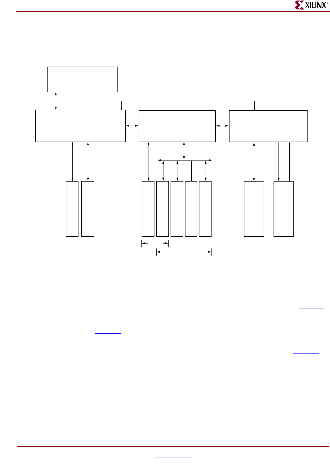
A high-level functional block diagram of the Virtex-5 FPGA ML561 Memory Interfaces
Development Board is shown in Figure 1-1.
The Virtex-5 FPGA ML561 Development Board includes the following major functional
blocks:
•Three XC5VLX50T-FFG1136 FPGAs (see DS100, Virtex-5 Family Overview)
•DDR400 components: 128 MB (32M x 32 bits) at 200 MHz clock speed. See XAPP851,
DDR SDRAM Controller Using Virtex-5 FPGA Devices.
•DDR2 DIMM: Five PC2-5300 DIMM sockets for up to 2 GB (128M x 144 bits). See
XAPP858, High-Performance DDR2 SDRAM Interface in Virtex-5 Devices.
•DDR2-667 components: 64 MB (16M x 32 bits) at 333 MHz clock speed
•QDRII memory: 16 MB (2M x 72 bits) at up to 300 MHz clock speed. See XAPP853,
QDR II SRAM Interface for Virtex-5 Devices.
•RLDRAM II memory: 64 MB (16M x 36 bits) at up to 300 MHz clock speed. See
XAPP852, RLDRAM II Memory Interface for Virtex-5 FPGAs.
•One DB9-M RS-232 port and one USB 2.0 port
•A System ACE™ CompactFlash (CF) Configuration Controller that allows storing
and downloading of up to eight FPGA configuration image files
•On-board power regulators with ±5% output margin test capabilities
Figure 1-1: Virtex-5 FPGA ML561 Development Board Block Diagram
DDR2 DIMM 72
72
RLDRAM II
(CIO)
36
QDRII SRAM
DDR2 SDRAM 32
32
FPGA #1
XC5VLX50T/
FFG1136
FPGA #2
XC5VLX50T/
FFG1136
DDR400 SDRAM
SSTL18/SSTL2 SSTL18 HSTL
External Interfaces:
System ACE Controller,
USB, RS-232, LCD
DDR2 DIMM
DDR2 DIMM
DDR2 DIMM
DDR2 DIMM
72
72
UG191_c1_01_020807
FPGA #3
XC5VLX50T/
FFG1136
WIDE
DEEP
Virtex-5 FPGA ML561 User Guide www.xilinx.com 13
UG199 (v1.2) April 19, 2008
Virtex-5 FPGA ML561 Memory Interfaces Development Board
R
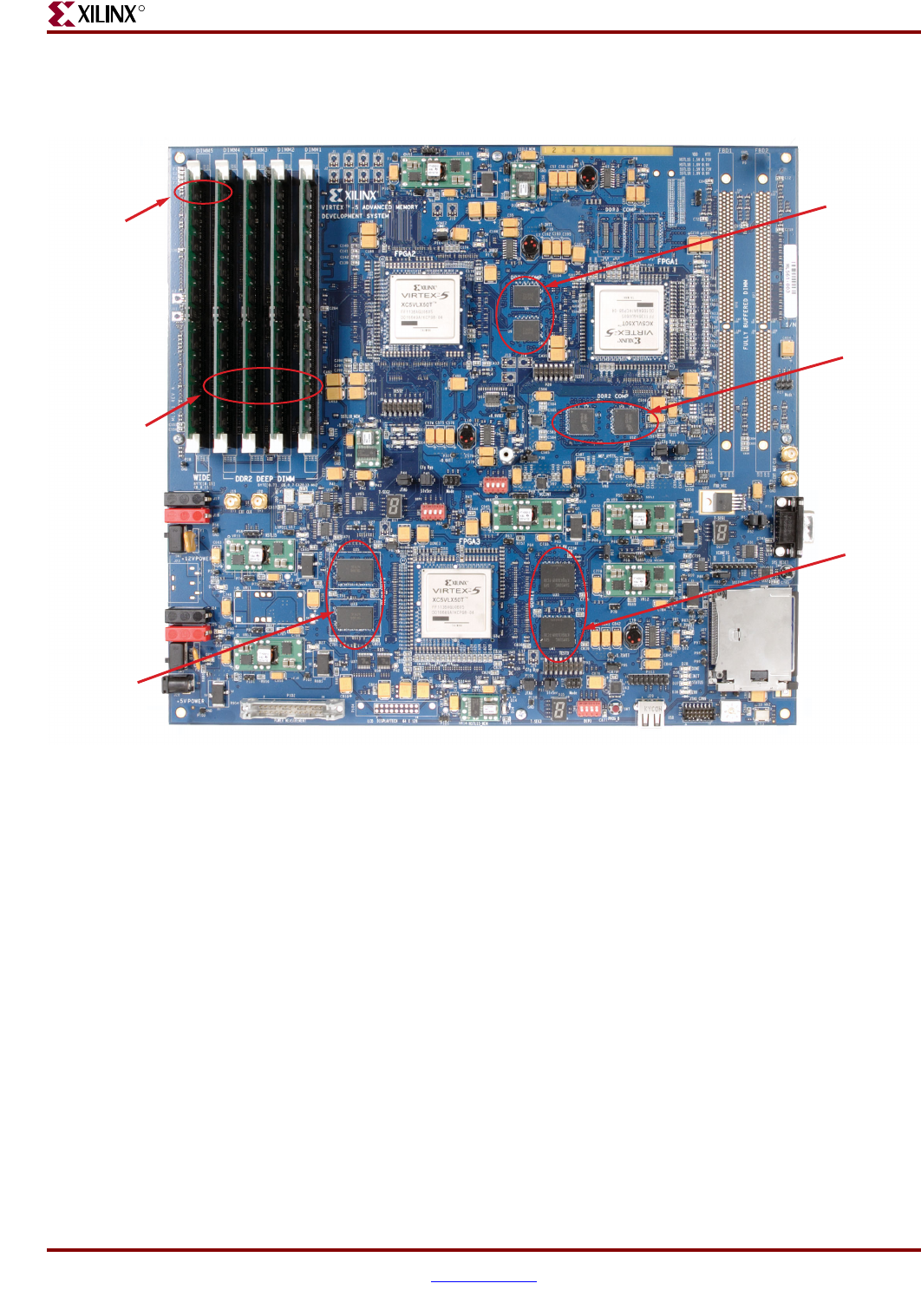
Figure 1-2 shows the Virtex-5 FPGA ML561 Development Board and indicates the
locations of the resident memory devices.
Figure 1-2: Virtex-5 FPGA ML561 Development Board
S A i l N 10 t hit / d h d F/L
DDR2
SDRAM
DIMM
32-bit
DDR400
SDRAM
32-bit
DDR2
SDRAM
72-bit
QDRII
SRAM
36-bit
RLDRAM II
144 bits wide
72 bits wide,
up to 4 deep
UG199_c1_02_050106


Virtex-5 FPGA ML561 User Guide www.xilinx.com 15
UG199 (v1.2) April 19, 2008
R
Chapter 2
Getting Started
This chapter describes the items needed to configure the Virtex-5 FPGA ML561 Memory
Interfaces Development Board. The Virtex-5 FPGA ML561 Development Board is tested at
the factory after assembly and should be received in working condition. It is set up to load
a bitstream from the CompactFlash card at socket J27 through the System ACE controller
(U45).
This chapter contains the following sections:
•“Documentation and Reference Design CD”
•“Initial Board Check Before Applying Power”
•“Applying Power to the Board”
Documentation and Reference Design CD
The CD included in the Virtex-5 FPGA ML561 Memory Interfaces Tool Kit contains the
design files for the Virtex-5 FPGA ML561 Development Board, including schematics,
board layout, and reference design files. Open the ReadMe.rtf file on the CD to review
the list of contents.
Initial Board Check Before Applying Power
Perform these steps before applying board power:
1. Set up the Configuration Mode jumpers (P27, P46, and P112) for JTAG configuration.
See “Configuration Modes” on page 51 for all available modes for the Virtex-5 FPGA
ML561 Development Board.
2. Confirm that the JTAG chain jumpers P38, P44, and P109 are connecting pins 1 to 2 and
pins 3 to 4. This way, all three devices are in the chain. Otherwise, the ISE iMPACT
software will not find all three devices to configure. For more information see “JTAG
Chain” on page 52.
3. Make sure that no inhibit jumpers are present on any of the power supply regulator
modules. For more information, see “Voltage Regulators” on page 34.
4. The Virtex-5 FPGA ML561 Development Board has a 200 MHz on-board oscillator,
which provides a copy of a differential LVPECL clock to each of the three FPGAs
through a differential clock buffer (ICS853006). There is also a connection to a pair of
SMA connectors (J19, J20) to provide a differential LVDS clock from an off-board signal
generator. Another differential clock buffer (ICS853006) provides a copy of this clock to
each of the three FPGAs. These clocks are available after configuration for the design to
use for various system clocks.

16 www.xilinx.com Virtex-5 FPGA ML561 User Guide
UG199 (v1.2) April 19, 2008
Chapter 2: Getting Started
R
5. Insert the CompactFlash card included in the kit into socket J27 on the Virtex-5 FPGA
ML561 Development Board. To select the startup file, check that SW8 is set to position
0.
Applying Power to the Board
The Virtex-5 FPGA ML561 Development Board is now ready to power on. The Virtex-5
FPGA ML561 Development Board is shipped with a country-specific AC line cord for the
universal input 5V desktop power supply. Follow these steps to power up the Virtex-5
FPGA ML561 Development Board:
1. Confirm that the ON-OFF switch, SW5, is in the OFF position.
2. Plug the 5V desktop power supply into the 5V DC input barrel jack J28 on the Virtex-5
FPGA ML561 Development Board. Plug the desktop power supply AC line cord into
an electrical outlet supplying the appropriate voltage.
3. Turn SW5 to the ON position. The power indicators for all regulator modules should
come on, indicating output from the regulators. The System ACE status LED D37
comes on when the System ACE controller (U45) extracts the BIT configuration file
from the CompactFlash card to the FPGA. If no CompactFlash card is installed in the
card socket J27 on the Virtex-5 FPGA ML561 Development Board, the red System ACE
error LED D38 flashes.
4. If a CompactFlash card is not installed in socket J27, a JTAG cable must be used to
configure the FPGAs. To use a Parallel IV cable or other JTAG pod, download the
FPGA configuration bitstream into each FPGA. After the DONE LED (D28) comes on,
the FPGAs are configured and ready to use.
5. Push the reset button SW4.

Virtex-5 FPGA ML561 User Guide www.xilinx.com 17
UG199 (v1.2) April 19, 2008
R
Chapter 3
Hardware Description
This chapter describes the major hardware blocks on the Virtex-5 FPGA ML561
Development Board and provides useful design consideration. It contains the following
sections:
•“Hardware Overview”
•“Memory Details”
•“External Interfaces”
•“Power Regulation”
•“Board Design Considerations”
Hardware Overview
The ML561 Development/Evaluation system reference design is implemented with three
XC5VLX50T-FFG1136 devices from the Virtex-5 FPGA family to demonstrate high-speed
external memory application interfaces. The memory technologies supported by the
Virtex-5 FPGA ML561 Development Board are DDR2 SDRAM, DDR400 SDRAM, QDRII
SRAM, and RLDRAM II SDRAM.
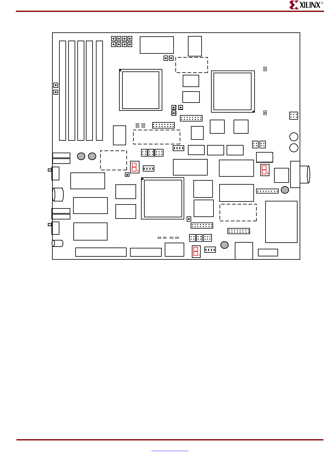
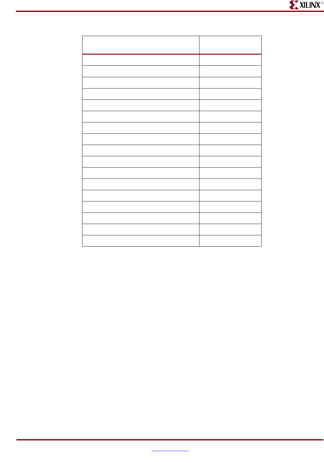
Figure 3-1 provides a view of all the major components on ML561 board. It shows the
placement of the three Virtex-5 FPGAs, and the position of the associated major interfaces
for each FPGA.
18 www.xilinx.com Virtex-5 FPGA ML561 User Guide
UG199 (v1.2) April 19, 2008
Chapter 3: Hardware Description
R
FPGA
The ML561 uses three Virtex-5 XC5VLX50T-FFG1136 devices, each in a 1136-pin,
35 mm x 35 mm BGA package. Figure 1-1, page 12 shows the memory devices associated
with the three FPGAs. Refer to Appendix A, “FPGA Pinouts,” for a complete pinout of all
Virtex-5 devices on the board. Refer to Appendix B, “Bill of Materials,” for a list of major
components on the Virtex-5 FPGA ML561 Development Board, including their reference
designators and links to their corresponding data sheets.
Figure 3-1: ML561 XC5VLX50T-FFG1136 Board Placement Diagram
HSTL
FPGA #3
FPGA #1
FPGA #2
SSTL18
HSTL
VTT & VREF
SSTL18
VTT & VREF
SSTL2
VTT & VREF
VCCAUX /
VCCO
VCCINT
USB
DIP3
DIP1
DIP2
7SEG3
7SEG2
7SEG1
Config3
PROG
External
CLK
5V Input
Jack
5V Banana
Jacks
12V Banana
Jacks
12V Input
Jack
SPY
SPY
ON
OFF
OFF
ON
RESET
SPY
Config1
Config2
SPY
SSTL2
JTAG
UG199_c3_01_050106
System ACE
Controller
FPGA #3 LEDs
FPGA #1
LEDs
FPGA #1
LEDs
FPGA #2
LEDs
JTAG Test Header
Test Header 3
A1
A1
A1
Test Header 2
Test Header 1
Serial Header
HSTL
12V -> 5V
RLDRAM II QDRII
QDRII
DDR2
AVTRX
AVC
CPLL
AVTTX
VVTTR
XC FBD
VCC
RS-232
Driver
DDR
DDR
DDR2 MGT
CLK
MGT Connections
RLDRAM II
Clocks &
Buffers
SSTL18
_M
DIMM1
DIMM2
DIMM3
DIMM4
DIMM5
SSTL2
_M
3.3V
LCD Connector
Pwr Measure Header
Virtex-5 FPGA ML561 User Guide www.xilinx.com 19
UG199 (v1.2) April 19, 2008
Hardware Overview
R
Memories
Table 3-1 lists the types of memories that the ML561 board supports.
When a larger data/strobe ratio is implemented, for example, a x36 QDRII device, the
smaller configurations can also be demonstrated by programming the FPGA for a smaller
data width, such as a 9:1 data/strobe ratio for the QDRII device.
DDR400 SDRAM Components
The Virtex-5 FPGA ML561 Development Board has two 200 MHz Micron
MT46V32M16BN-5B (16-bit) DDR400 SDRAM components that provide a 32-bit interface.
Each 16-bit device is packaged in a 60-ball FBGA package, with a common address and
control bus and separate clocks and DQS/DQ signals.
DDR2 DIMM
The Virtex-5 FPGA ML561 Development Board contains five PC-5300 240-pin DIMM
sockets for a maximum data width of 144 bits or a maximum depth of four DIMMs. The
sockets are arranged in a row leading away from the FPGA so they can share common
address and control signals. DIMM1 through DIMM4 share DQ/DQS signals to form a
deep 72-bit memory interface, while DIMM5 has separate DQ/DQS signals.
For the deep DDR2 interface, the sockets are to be populated starting at socket DIMM4.
Table 3-2 illustrates how the sockets should be populated based on the interface wanted.
Populating the DIMMs in this order is necessary due to the placement of the termination
on the signals being shared. More detail on termination is given in “Board Design
Considerations,” page 36.
Table 3-1: Summary of ML561 Memory Interfaces
Memory Type Maximum Speed Data Rate Data Width I/O Standard Data/Strobe
Ratios
DDR400 SDRAM 200 MHz 400 Mbps 32 SSTL2 8:1
DDR2 DIMM 333 MHz 667 Mbps 144 SSTL18 8:1
DDR2 SDRAM 333 MHz 667 Mbps 32 SSTL18 8:1
QDRII SRAM 300 MHz 1.2 Gbps 72 HSTL18 18:1, 36:1
RLDRAM II 300 MHz 600 Mbps 36 HSTL18 9:1, 18:1
Table 3-2: Populating DDR2 DIMM Sockets
DIMM Interface DIMM Sockets
Populated Interface Width
One Deep 5 or 4 72-bit
Two Deep 4 and 3 72-bit
Three Deep 4, 3, and 2 72-bit
Four Deep 4, 3, 2, and 1 72-bit
Two Wide 5 and 4 144-bit
20 www.xilinx.com Virtex-5 FPGA ML561 User Guide
UG199 (v1.2) April 19, 2008
Chapter 3: Hardware Description
R
DDR2 SDRAM Components
The ML561 board contains two 333 MHz Micron MT47H32M16CC-3 (16-bit) DDR2
SDRAM components that provide a 32-bit interface to FPGA #1. Each 16-bit device is
packaged in an 84-ball FBGA package, with a common address and control bus and
separate clocks and DQS/DQ signals.
QDRII SRAM
The ML561 board contains a 300 MHz QDRII SRAM interface with a 72-bit Read interface
and a 72-bit Write interface using two Samsung K7R643684M-FC30 components (x36).
They are packaged in a 165-ball FBGA package with a body size of 15 x 17 mm. These two
components share the same address/control signals but have separate clock and data
signals.
RLDRAM II Devices
The ML561 contains a 300 MHz 36-bit RLDRAM II interface using two Micron
MT49H16M18BM-25 devices (x18) packaged in a 144-ball PBGA package. They share a
common address and control bus but have separate clocks and DQS/DQ signals.
Figure 3-2: DDR2 Deep and Wide DIMM Sockets
DIMM1 (XP5)
DIMM2 (XP4)
DIMM3 (XP3)
DIMM4 (XP2)
DIMM5 (XP1)
DQ and DQS
BY0-BY7, CB0_7
DQ and DQS
BY8-BY15, CB8_15
Address and Commands
DIMM1 Control
Wide
Deep
DIMM2 Control
DIMM3 Control
DIMM4 Control
DIMM5 Control
UG199_c3_02_050106
Virtex-5 FPGA ML561 User Guide www.xilinx.com 21
UG199 (v1.2) April 19, 2008
Memory Details
R
Memory Details
DDR400 and DDR2 Component Memories
The FPGA #1 device on the Virtex-5 FPGA ML561 Development Board is connected to
DDR and DDR2 component memories, as shown in Figure 3-3.
Figure 3-3 summarizes the distribution of DDR and DDR2 discrete component interface
signals among the different banks of the FPGA #1 device.
Figure 3-3: FPGA #1 Banks for DDR400 and DDR2 Component (Top View)
BANK 21 (40)
BANK 13 (40)
DDR Components
DQ 0, 1, 2
BANK 114
BANK 112
BANK 11 (40)
DDR Components
DQ 3 & Controls
BANK 12 (40)
USB Controls
BANK 17 (40) BANK 18 (40) BANK 118
BANK 22 (40) BANK 122
BANK 126
(Configuration)
BANK 0
BANK 4 (20)
Global Clock Inputs
BANK 25 (40) BANK 6 (20)
GTP I/O
BANK 2 (20)
Voltage Control
BANK 15 (40)
DDR2 Component
DQ 0, 1
BANK 116
BANK 19 (40)
DDR2 Component
DQ 2, 3
BANK 120BANK 20 (40)
RS232
Inter-FPGA MII Links
BANK 1 (20)
DDR2 Component
Address
BANK 23 (40) BANK 124BANK 5 (20)
BANK 3 (20)
DDR2 Component
Controls
UG199_c3_03_050106
22 www.xilinx.com Virtex-5 FPGA ML561 User Guide
UG199 (v1.2) April 19, 2008
Chapter 3: Hardware Description
R
Table 3-3 describes all signals associated with DDR400 Component memories.
Table 3-4 describes all signals associated with DDR2 Component memories. For a complete
list of FPGA #1 signals and their pin locations, refer to Appendix A, “FPGA Pinouts.”
XAPP851, DDR SDRAM Controller Using Virtex-5 FPGA Devices, XAPP858, High-
Performance DDR2 SDRAM Interface in Virtex-5 Devices, and the corresponding demos are
included on the CD shipped with the ML561 Tool Kit. For a complete list of FPGA #1
signals and their pin locations, refer to Appendix A, “FPGA Pinouts.”
Table 3-3: DDR400 Component Signal Summary
Board Signal Name(s) Bits Description
DDR1_A[13:0] 14 DDR400 Component Address
DDR1_CK[2:1]_[P,N] 4 DDR400 Component Differential Clock
DDR1_[RAS,CAS,WE]_N, DDR1_CKE,
DDR1_BA[1:0], DDR1_BY[0_1,2_3]_CS_N,
DDR1_DM_BY[3:0]
12 DDR400 Component Control Signals
DDR1_DQ_BY0_B[7:0], DDR1_DQS_BY0_P 9 DDR400 Data and Strobe: Byte 0
DDR1_DQ_BY1_B[7:0], DDR1_DQS_BY1_P 9 DDR400 Data and Strobe: Byte 1
DDR1_DQ_BY2_B[7:0], DDR1_DQS_BY2_P 9 DDR400 Data and Strobe: Byte 2
DDR1_DQ_BY3_B[7:0], DDR1_DQS_BY3_P 9 DDR400 Data and Strobe: Byte 3
Notes:
1. DDR1_CKE signal has a weak 4.7KΩ pull-down resistor to meet the memory power-up requirements.
Table 3-4: DDR2 Component Signal Summary
Board Signal Name(s) Bits Description
DDR2_A[12:0] 13 DDR2 Component Address
DDR2_CK[1:0]_[P,N] 4 DDR2 Component Differential
Clock
DDR2_ODT[1:0], DDR2_[RAS,CAS,WE]_N,
DDR2_CKE, DDR2_BA[1:0], DDR2_CS[1:0]_N,
DDR2_DM_BY[3:0]
14 DDR2 Component Control Signals
DDR2_DQ_BY0_B[7:0], DDR2_DQS_BY0_[P,N] 10 DDR2 Data and Strobe: Byte 0
DDR2_DQ_BY1_B[7:0], DDR2_DQS_BY1_[P,N] 10 DDR2 Data and Strobe: Byte 1
DDR2_DQ_BY2_B[7:0], DDR2_DQS_BY2_[P,N] 10 DDR2 Data and Strobe: Byte 2
DDR2_DQ_BY3_B[7:0], DDR2_DQS_BY3_[P,N] 10 DDR2 Data and Strobe: Byte 3
Notes:
1. DDR2_CKE and DDR2_ODT[1:0] signals have a weak 4.7KΩ pull-down resistor to meet the memory
power-up requirements.
Virtex-5 FPGA ML561 User Guide www.xilinx.com 23
UG199 (v1.2) April 19, 2008
Memory Details
R
DDR2 SDRAM DIMM
The FPGA #2 device on the Virtex-5 FPGA ML561 Development Board is connected to
DDR2 memories. The DDR2 memory interface includes a 144-bit wide DIMM connection
to up to five 240-pin DDR2 DIMM sockets.
For the 144-bit wide DIMM datapath, the data bytes are spread across multiple banks of
the FPGA #2 device. Figure 3-4 summarizes the distribution of DDR2 DIMM interface
signals among the different banks of the FPGA #2 device.
Figure 3-4: FPGA #2 Banks for DDR2 DIMM (SSTL18) Interfaces (Top View)
BANK 20 (40)
DDR2 DIMM
DQ 8, 9, 10
BANK 12 (40)
DDR2 DIMM
DQ 11, 12, CB8_15
BANK 11 (40)
DDR2 DIMM
DQ 6, 3 CB0_7
BANK 112
BANK 114 BANK 13 (40)
DDR2 DIMM
DQ 5, 7, 4
BANK 15 (40)
DDR2 DIMM
DQ 0, 1, 2
BANK 116
GTP CLK
BANK 19 (40)
DDR2 DIMM
Controls & DIMM1 Cntl
BANK 120
RX 0, 1
(Configuration)
BANK 0
BANK 3 (20)
General I/O
BANK 5 (20) BANK 23 (40)BANK 124
TX 0, 1
BANK 1 (20)
General I/O
BANK 18 (40)
DDR2 DIMM
DQ 14, 15, 13
BANK 17 (40)
DDR2 DIMM
Common Controls
BANK 118
BANK 22 (40)
DDR2 DIMM
DIMM 4 & 5 Cntl
BANK 122 BANK 21 (40)
DDR2 DIMM
DIMM 1, 2, 3 Cntl
BANK 2 (20)
Inter-FPGA MII Links
BANK 25 (40)BANK 126 BANK 6 (20)
BANK 4 (20)
Global Clock Inputs
UG199_c3_04_050106
24 www.xilinx.com Virtex-5 FPGA ML561 User Guide
UG199 (v1.2) April 19, 2008
Chapter 3: Hardware Description
R
Table 3-5 describes all the signals associated with DDR2 DIMM component memories. For
the Deep DIMM interface to four DIMMs, the individual dedicated control signals are
listed at the bottom of Table 3-5.
XAPP858, High-Performance DDR2 SDRAM Interface in Virtex-5 Devices and its
corresponding demo are included on the CD shipped with the ML561 Tool Kit.
Table 3-5: DDR2 DIMM Signal Summary
Board Signal Name(s) Bits Description
DDR2_DIMM_A[15:0] 16 DDR2 DIMM Address
DDR2_DIMM[5:1]_CK[2:0]_[P,N] 30 DDR2 DIMM Differential Clocks: Three copies per
DIMM
DDR2_DIMM_[RAS,CAS,WE,RESET]_N,
DDR2_DIMM[5:1]_CKE[1:0], DDR2_DIMM_BA[2:0],
DDR2_DIMM[5:1]_CS[1:0]_N,
DDR2_DIMM[5:1]_ODT[1:0]
37 DDR2 DIMM Common Control Signals
DDR2_DIMM[1:5]_CS[1:0]_N,
DDR2_DIMM[1:5]_CKE[1:0],
DDR2_DIMM[1:5]_ODT[1:0]
20 DDR2 DIMM Dedicated Control Signals
DDR2_DIMM_LB_BK[11,13,15]_[IN,OUT] 6 Deep DIMMs (DIMM1 through DIMM4) Loopback
Signals
DDR2_DIMM_LB_BK[12,18,20] 3 Wide DIMM (DIMM5) Loopback Signals (Total of six
FPGA pins)
DDR2_DIMM[1:5]_CNTL_PAR,
DDR2_DIMM[1:5]_CNTL_PAR_ERR,
DDR2_DIMM[1:5]_NC_019, DDR2_DIMM[1:5]_NC_102
20 Miscellaneous Place Holder Signals to the Five
DIMMs
DDR2_DIMM_DQ_BY[0:15]_B[7:0],
DDR2_DIMM_DQS_BY[0:15]_L_[P,N],
DDR2_DIMM_DM_BY[0:15]
176 DDR2 DIMM Data, Strobes, and Data Mask: Bytes 0
through 15
DDR2_DIMM_DQ_CB0_7_B[7:0],
DDR2_DIMM_DQS_CB0_7_L_[P,N],
DDR2_DIMM_DM_CB0_7
11 DDR2 DIMM Data, Strobes, and Data Mask: Check
Byte 0
DDR2_DIMM_DQ_CB8_15_B[7:0],
DDR2_DIMM_DQS_CB8_15_L_[P,N],
DDR2_DIMM_DM_CB8_15
11 DDR2 DIMM Data, Strobes, and Data Mask: Check
Byte 1
DDR2_DIMM[1:5]_SA[2:0] 15 Serial PROM Address
DDR2_DIMM_[SCL,SDA]" 2 Serial PROM interface CLK and Data
Notes:
1. DDR2_DIMM_CKE and DDR2_DIMM_ODT signals are connected to a 4.7KΩ pull-down resistor to meet the memory power-up
requirements.
Virtex-5 FPGA ML561 User Guide www.xilinx.com 25
UG199 (v1.2) April 19, 2008
Memory Details
R
QDRII and RLDRAM II Memories
Figure 3-5 summarizes the distribution of QDRII and RLDRAM II component interface
signals among the different banks of the FPGA #3 device.
Figure 3-5: FPGA #3 Banks for QDRII SRAM and RLDRAM II Interfaces (Top View)
BANK 20 (40)
RLDII Data
DQ 0, 1 & D0
BANK 12 (40)
RLDII Data
DQ 2, 3 & D1
BANK 11 (40)
QDRII Data
Q0, 2 & D6
BANK 112
BANK 114 BANK 13 (40)
QDRII Data
Q4, 5, 6
BANK 15 (40)
QDRII Data
D7, 2, 3, 0
BANK 116
BANK 19 (40)
QDRII Data
Q1, 3 & D1
BANK 120
(Configuration)
BANK 0
BANK 3 (20)
General I/O
BANK 5 (20) BANK 23 (40)BANK 124
BANK 1 (20)
System ACE Controls
BANK 18 (40)
RLDII Data
D 2, 3
BANK 17 (40)
QDRII Data
Q7 & D4, 5
BANK 118
BANK 22 (40)
RLDII Address
and Control
BANK 122 BANK 21 (40)
QDRII Address
and Control
BANK 2 (20)
Inter-FPGA MII Links
BANK 25 (40)BANK 126 BANK 6 (20)
BANK 4 (20)
Global Clock Inputs
UG199_c3_05_050106
26 www.xilinx.com Virtex-5 FPGA ML561 User Guide
UG199 (v1.2) April 19, 2008
Chapter 3: Hardware Description
R
Table 3-6 describes all the signals associated with QDRII component memories.
XAPP853: QDR II SRAM Interface for Virtex-5 Devices and its corresponding demo are
included on the CD shipped with the ML561 Tool Kit.
For a complete list of FPGA #3 signals and their pin locations, refer to Appendix A, “FPGA
Pinouts.”
Table 3-7 describes all signals associated with RLDRAM II devices.
XAPP852, RLDRAM II Memory Interface for Virtex-5 FPGAs and its corresponding demo are
included on the CD shipped with the ML561 Tool Kit.
Table 3-6: QDRII Component Signal Summary
Board Signal Name(s) Bits Description
QDR2_SA[18:0] 19 QDRII Address
QDR2_CK_BY0_3_[P,N],
QDR2_CK_BY4_7_[P,N]
4QDRII Differential Clock
QDR2_[R,W,DLL_OFF]_N 3 QDRII Control Signals
QDR2_D_BY[3:0]_B[8:0],
QDR2_K_BY0_3_[P,N],
QDR2_BW_BY[3:0]
42 QDRII Write Data, Strobes, and Byte Write: Bytes 3:0
QDR2_Q_BY[3:0]_B[8:0],
QDR2_CQ_BY0_3_[P,N]
38 QDRII Read Data and Strobes: Bytes 3:0
QDR2_D_BY[7:4]_B[8:0],
QDR2_K_BY4_7_[P,N],
QDR2_BW_BY[3:0]
42 QDRII Write Data, Strobes, and Byte Write: Bytes 7:4
QDR2_Q_BY[7:4]_B[8:0],
QDR2_CQ_BY4_7_[P,N]
38 QDRII Read Data and Strobes: Bytes 7:4
Notes:
1. QDR2_SA[18] is incorrectly labeled QDR2_NC_A3 in the ML561 schematics and layout file.
Table 3-7: RLDRAM II Component Signal Summary
Board Signal Name(s) Bits Description
RLD2_A[19:0], RLD2_BA[2:0] 23 RLDRAM II Address
RLD2_CK_BY0_1 _[P,N] 2 RLDRAM II Differential Clock
RLD2_CK_BY2_3 _[P,N] 2 RLDRAM II Differential Clock
RLD2_CS_BY[0_1,2_3]_N, RLD2_[REF,WE]_N,
RLD2_DM_BY[0_1,2_3]_N, RLD2_QVLD_BY[0_1,2_3]
8 RLDRAM II Control Signals
RLD2_DQ_BY[1:0]_B[8:0], RLD2_DK_BY0_1_[P,N],
RLD2_QK_BY[1:0]_[P,N]
24 RLDRAM II Data and Strobes: Bytes 1:0
RLD2_DQ_BY[3:2]_B[8:0], RLD2_DK_BY0_1_[P,N],
RLD2_QK_BY[3:2]_[P,N]
24 RLDRAM II Data and Strobes: Bytes 3:2
Virtex-5 FPGA ML561 User Guide www.xilinx.com 27
UG199 (v1.2) April 19, 2008
External Interfaces
R
External Interfaces
The external interfaces of the Virtex-5 FPGA ML561 Development Board are described in
this section.
RS-232
The ML561 board provides an RS-232 serial interface using a Maxim MAX3316ECUP
device. The maximum speed of this device is 460 Kbps.
Hooks are provided to connect and disconnect FPGAs to the RS-232 serial interface, by
placing jumpers on headers based on the FPGA involved in the communication. Only one
FPGA is allowed in the communication, and others must be disconnected before operation.
The ML561 toolkit CD contains code to implement a UART core in one FPGA for
interfacing with a host PC.
The RS-232 interface is accessible through a male DB-9 serial connector (P73).
USB
Full-speed (12 Mbps) USB functionality is proved using a Silicon Laboratories CP2102-GM
USB to RS-232 Bridge. RS-232 and USB signals are converted between one another so a
RS-232 core needs to be implemented in the FPGA for communication. A level translator is
used to convert between the 2.5V I/O of the FPGA and the 3.3V I/O the CP2102 uses.
Hooks are provided to connect and disconnect FPGAs to the USB connection, by placing
jumpers on headers based on the FPGA involved in the communication. Only one FPGA is
allowed in the communication, and others must be disconnected before operation.
The USB interface is accessible through a female ‘A’ USB connector (J29).
Clocks
The ML561 board contains a 200 MHz LVPECL clock oscillator and connectors for external
clock inputs for use as system clocks (J19 and J20). The GTP transceivers use their own
clock source that can be provided through SMA connectors on the board (J16 and J21).
Table 3-8: RS-232 Jumper Settings
To Connect FPGA # to
DB-9 (P73) TX RX
FPGA #1 P52 Pin 2 -> P52 Pin 1 P53 Pin 2 -> P53 Pin 1
FPGA #2 P52 Pin 2 -> P51 Pin 1 P53 Pin 2 -> P54 Pin 1
FPGA #3 P52 Pin 2 -> P52 Pin 3 P53 Pin 2 -> P53 Pin 3
Table 3-9: USB Jumper Settings
To Connect FPGA # to DB-9
(J29) TX RX
FPGA #1 P36 Pin 2 -> P36 Pin 1 P22 Pin2 -> P22 Pin 1
FPGA #2 P36 Pin 2 -> P35 Pin 1 P22 Pin2 -> P23 Pin 1
FPGA #3 P36 Pin 2 -> P36 Pin 3 P22 Pin2 -> P22 Pin 3
28 www.xilinx.com Virtex-5 FPGA ML561 User Guide
UG199 (v1.2) April 19, 2008
Chapter 3: Hardware Description
R
200 MHz LVPECL Clock
The 200 MHz LVPECL clock source is an Epson EG-2121CA200M-PCHS oscillator (Y1)
with a differential output. The oscillator runs at 200 MHz ± 100 PPM with an operating
voltage of 2.5V ±5%. This output is fed into an ICS853006 LVPECL buffer for generating a
separate differential copy for each FPGA as well as a test point (P59).
SMA Clock
Two SMA connectors are provided for the input of an off-board differential clock (J19 and
J20). A differential clock buffer (ICS853006) is used on the board (U17 and U18) to generate
four LVPECL copies of the differential clock signal, one for each FPGA along with a probe
point (P40) for testing. The traces from the buffer are routed as a differential pair to each
FPGA where they are terminated with 100Ω differential termination.
33 MHz Clock
A single-ended 33 MHz Epson SG-8002CA oscillator is provided on the board (Y2) for
testing purposes. Four copies of this clock are generated using a clock buffer (ICS8304) on
the board, one per FPGA along with a probe point for testing (P41).
The application using this clock source as an input to the PLL on the Virtex-5 device has
not yet been fully verified.
Table 3-10: FPGA 200 MHz IDELAY Reference Clock Source
FPGA # Signal Name
1 DIRECT_CLK_TO_FPGA1_P
1 DIRECT_CLK_TO_FPGA1_N
2 DIRECT_CLK_TO_FPGA2_P
2 DIRECT_CLK_TO_FPGA2_N
3 DIRECT_CLK_TO_FPGA3_P
3 DIRECT_CLK_TO_FPGA3_N
Table 3-11: FPGA External Clock Sources
FPGA # Signal Name
1 EXT_CLK_TO_FPGA1_P
1 EXT_CLK_TO_FPGA1_N
2 EXT_CLK_TO_FPGA2_P
2 EXT_CLK_TO_FPGA2_N
3 EXT_CLK_TO_FPGA3_P
3 EXT_CLK_TO_FPGA3_N
Virtex-5 FPGA ML561 User Guide www.xilinx.com 29
UG199 (v1.2) April 19, 2008
External Interfaces
R
33 MHz System ACE Controller Oscillator
A single-ended 33 MHz Epson SG-8002CA oscillator is provided on the board (Y3) as a
clock source for System ACE functionality.
GTP Clocks
Two SMA connectors are provided for the input of an off-board differential clock (J16 and
J21). A differential clock buffer (ICS8543BG) is used on the board (U20) to generate four
LVDS copies of the differential clock signal, two for FPGA #1, one for FPGA #2, and one for
FPGA #3.
A header is used to select between a clock forwarded by the GTP or from the external clock
source used to provide a clock to the FPGA logic.
User I/Os
This subsection describes the devices that connect to the User I/Os of the ML561 board.
These I/Os are provided to ease hardware development using the ML561.
General-Purpose Headers
The 16-pin test headers are surface mounted, one per FPGA. Of the two bytes of test
signals, traces are matched for signals within a byte.
DIP Switch
One four-position DIP switch per FPGA (for a total of three) is available to externally pull
up or pull down a signal on the FPGA. This can be used to manually set values used by the
design running on the FPGA.
Table 3-12: FPGA Slow Clock Sources
FPGA Signal Name
1 FPGA1_LOW_FREQ_CLK
2 FPGA2_LOW_FREQ_CLK
3 FPGA3_LOW_FREQ_CLK
Table 3-13: Test Headers
Header Signal Description Location Header Pin #
FPGA1_TEST_HDR_BY0_B[0:7] P20 (TEST1) Odd pins: 1, 3, 5, 7, 9, 11, 13, 15
FPGA1_TEST_HDR_BY1_B[0:7] P20 (TEST1) Even pins: 2, 4, 6, 8, 10, 12, 14, 16
FPGA2_TEST_HDR_BY0_B[0:7] P21 (TEST2) Odd pins: 1, 3, 5, 7, 9, 11, 13, 15
FPGA2_TEST_HDR_BY1_B[0:7] P21 (TEST2) Even pins: 2, 4, 6, 8, 10, 12, 14, 16
FPGA3_TEST_HDR_BY0_B[0:7] P93 (TEST3) Odd pins: 1, 3, 5, 7, 9, 11, 13, 15
FPGA3_TEST_HDR_BY1_B[0:7] P93 (TEST3) Even pins: 2, 4, 6, 8, 10, 12, 14, 16
30 www.xilinx.com Virtex-5 FPGA ML561 User Guide
UG199 (v1.2) April 19, 2008
Chapter 3: Hardware Description
R
Seven-Segment Displays
One seven-segment display per FPGA (for a total of three) is available for use. The red
Stanley-Electric NAR131SB displays are active Low, using seven inputs to display a
character or number plus another input for a decimal point.
Light Emitting Diodes (LEDs)
Each FPGA is able to control four active-high green LEDs. The green is used to distinguish
the User LEDs from the blue system LEDs on the Virtex-5 FPGA ML561 Development
Board.
Pushbuttons
The ML561 board contains two momentary pushbuttons. Their functions and locations are
described in Table 3-14.
The Reset signal goes to a buffer (U32) that provides a separate copy of Reset to each
FPGA.
Figure 3-6: Seven-Segment Display Signal Mapping
7SEG_5_N 7SEG_1_N
7SEG_0_N
7SEG_6_N
7SEG_3_N
7SEG_4_N 7SEG_2_N
7SEG_DP_N
UG199_c3_06_050106
Table 3-14: User Pushbuttons
Button Description Pin Connection
SW7 PROG_B: Configure FPGA System ACE Controller: Pin 33
SW4 RESET_N: Reset the FPGA designs FPGA #1: AH14
FPGA #2: AH14
FPGA #3: AH14
Virtex-5 FPGA ML561 User Guide www.xilinx.com 31
UG199 (v1.2) April 19, 2008
External Interfaces
R
Power On or Off Slide Switch
The power on or off slide switch is a DPST slide switch used to apply input power to the
board. While the board contains two such switches, the 5V switch is primarily used to
supply 5V power to the board, whereas the 12V switch is available for testing only.
Soft Touch Probe Points
Soft Touch E5396A Probeless connection points are provided for monitoring FPGA #2 and
FPGA #3 test signals with a compatible Agilent logic analyzer. FPGA #2 uses separate test
signals for soft touch pins, while FPGA #3 shares the general-purpose test header signals
with soft touch pins due to lack of available I/O pins.
Power Measurement Header
The ML561 comes with a 3M Pak 100 power measurement header to enable easy
measurement of the power being consumed by the devices on the ML561. Each power
regulator uses an Isotek Kelvin current sense resistor (SMV-R010-0.5) in the path from the
output of the regulator to the power plane. The power can be computed by measuring the
voltage drop across each of these resistors.
Figure 3-7: Virtex-5 FPGA ML561 Development Board Power Measurement System
Table 3-15: Power Measurement Header Pins (P102)
Header Signal Power Header Pin #
VCC1V0_SENSE+ 1
VCC1V0_SENSE- 2
VCC1V0_MON 3
VCC2V5_SENSE+ 5
VCC2V5_SENSE- 6
VCC2V5_MON 7
VCC3V3_SENSE+ 9
VCC3V3_SENSE- 10
VCC3V3_MON 11
UG199_c3_07_050106
MARGIN+ MARGIN-
Voltage
Regulator
RSET
VIN VOUT
+5V or +12V To FPGA or
Other Device
To
Monitor
Cable
VCCXX Sense-
VCCXX Sense+
VCCXX Mon
VCCX
RKELVIN = 10 mΩ
1KΩ
VCCXXPR
32 www.xilinx.com Virtex-5 FPGA ML561 User Guide
UG199 (v1.2) April 19, 2008
Chapter 3: Hardware Description
R
Liquid Crystal Display Connector
Previous memory boards such as the ML461 had a DisplaytechQ 64128E-FC-BC-3LP
64x128 LCD panel. This display was removed from the ML561, but the connection is still
available for use with embedded systems if the user connects the display to connector
(P104). The LCD panel needs to hang off the edge of the board as shown in Figure 3-8.
VCC1V8_SENSE+ 13
VCC1V8_SENSE- 14
VCC1V8_MON 15
VCC1V5_SENSE+ 17
VCC1V5_SENSE- 18
VCC1V5_MON 19
VCC2V6_SENSE+ 21
VCC2V6_SENSE- 22
VCC2V6_MON 23
VCC5_SENSE+ 25
VCC5_SENSE- 26
VCC5_MON 24
VCC5 20
GND 4
GND 8
GND 12
GND 16
Table 3-15: Power Measurement Header Pins (P102) (Continued)
Header Signal Power Header Pin #
Virtex-5 FPGA ML561 User Guide www.xilinx.com 33
UG199 (v1.2) April 19, 2008
Power Regulation
R
The product specification at
http://www.displaytech.com.hk/pdf/graphic/64128e%20series-v10.PDF provides more
information. Appendix C, “LCD Interface,” describes the LCD operation in detail.
Power Regulation
This section describes the devices that supply power to the Virtex-5 FPGA ML561
Development Board. For electrical requirements and power consumption, see Chapter 4,
“Electrical Requirements.”
Power Distribution
The ML561 board uses +5V to drive numerous voltage regulators. Figure 3-9 shows a
general overview of the power distribution system.
The Virtex-5 FPGA ML561 Development Board is powered through the +5V input jack
(J28) from the power supply included in the ML561 Tool Kit. Alternatively, the +5V can
Figure 3-8: LCD Panel Connector for Possible LCD Support
HSTL
FPGA3
HSTL
VTT & VREF
VCCAUX /
VCCO
USB
DIP3
7SEG3
7SEG1
Config3
PROG
5V Input
Jack
5V Banana
Jacks
12V Input
Jack
SPY
SPY
OFF
OFF
ON
RESET
JTAG
UG199_c3_08_050106
System ACE
Controller
FPGA3 LEDs
JTAG Test Header
Test Header 3
A1
Serial Header
HSTL
12V -> 5V
RLDRAM II QDRII
QDRII
RS232
Driver
RLDRAM II
3.3V
LCD Connector
Pwr Measure Header
LCD
Figure 3-9: Virtex-5 FPGA ML561 Development Board Power Distribution System
Board Power
3.3V
FPGA Power
VCCINT or VCCAUX/VCCO
VTT VTT
To FPGAs
To All FPGAs
To Memories
To Devices
VREF VREF
MGT
Power MGT Power
12V -> 5V
+12V
+5V
Slide
Switch
Slide
Switch
FPGA Power
SSTL18, HSTL, or SSTL2
Memory Power
SSTL18, HSTL, or SSTL2
UG199_c3_09_050106
34 www.xilinx.com Virtex-5 FPGA ML561 User Guide
UG199 (v1.2) April 19, 2008
Chapter 3: Hardware Description
R
also be supplied from a bench supply using the two banana jacks: J25 (RED) for +5V and
J24 (BLACK) for GND.
The Rev-A assembly of the Virtex-5 FPGA ML561 Development Board does not support
the +12V input via jack J23 or via banana jacks J18 (RED) for +12V and J17 (BLACK) for
GND.
The memory and FPGAs use separate power supplies for SSTL18, HSTL, and SSTL2,
respectively. Thus the power being consumed can be easily measured for each using the
power measurement header provided on the ML561.
Voltage Regulators
The +5V voltage source is supplied as input to nine on-board regulator modules. Six of
those modules (TI PTH05010-WAZ) are used to generate the +1.0V, +2.5V, and +1.8V for
SSTL18 at FPGA #1 and FPGA #2, +1.8V for HSTL18 at FPGA #3, +2.6V for SSTL2 at
FPGA #1, and +3.3V voltages for the GTP power supplies, LEDs, etc. The remaining three
modules (TI PTH05000-ADJ) are used to generate +1.8V for SSTL18 at the memories, +1.8V
for HSTL at the memories, and +2.6V for SSTL2 at the memories.
An additional three bulk voltage regulators (Fairchild FN6555) are used to generate
termination (VTT) and reference (VREF) voltages each for the SSTL2, SSTL18, and HSTL
power levels. By design, these voltage levels are half of the input reference voltage being
supplied by the memory power supplies.
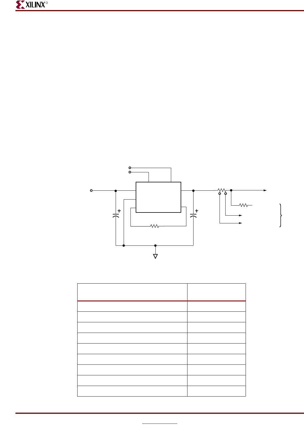
The TI PTH05010-WAZ and TI PTH05000-ADJ regulator modules require a fixed 5V input.
The output is adjustable over a range of 0.9V to 3.6V by changing the resistor tied between
pin 4 and GND. The difference between these two modules is that the PTH05010-WAZ
output voltage can be margined up to+ 5% of the nominal value by driving pin 10 to GND
(or digital Low), or margined down to -5% of the nominal value by driving pin 9 Low. The
PTH05010-WAZ also has a tracking feature that can be used to track another voltage
source.
There are two ways to apply the digital controls to the margin input pins of the PTH05010:
either from FPGA #1 or manually with jumpers.
Figure 3-10: PTH05010 Voltage Regulator
PTH05010
Voltage Regulator
VIN
GND TRACK MRGNUP MRGNDN GND
CIN RSET
470 μF
COUT
330 μF
(optional)
VOUT
5V
+ +
1
2
3 5 4
6
7
8 9 10
Inhibit
Jumper
INHIBIT VO_ADJ VO_SENSE
VMARGIN_UP_xxxx_N
VMARGIN_DN_xxxx_N
TRACK
UG199_c3_10_050106
Virtex-5 FPGA ML561 User Guide www.xilinx.com 35
UG199 (v1.2) April 19, 2008
Power Regulation
R
The FPGA can drive VMARGIN_DN_xxxx_N and VMARGIN_UP_xxxx_N signals, where
xxxx indicates one of the six main power regulators: SSTL2, HSTL, SSTL18, VCC1V0,
VCC2V5, and VCC3V3.
If both voltage-margining inputs to the power regulator are pulled Low, the output voltage
is close to nominal but has the possibility of a slightly higher error in the output voltage.
The power modules use a low-leakage open-drain control signal to control the voltage
margining. In the FPGA, this can be approximated by using a control signal that drives the
output Low when active and does not drive the signal at all when inactive (high-
impedance output).
Three-pin headers are available for performing manual voltage margining, using jumpers
to select between Nominal, -5%, and +5%. Table 3-17 shows the jumper settings.
The TI PTH05010-WAZ and TI PTH05000-ADJ regulator outputs can be enabled or
inhibited through the use of on-board two-pin jumpers. The inhibit jumpers use the
following conventions:
•Jumper OFF = Enabled
•Jumper ON = Inhibited
Table 3-16: Manual Voltage Margining
VMARGIN_UP_N VMARGIN_DN_N Output Voltage
High High Nominal
High Low -5%
Low High +5%
Low Low Not Applicable
Table 3-17: FPGA #1 Signals and On-Board Jumpers for Voltage Margining
Power Regulator Signal Name Jumper Setting
VCCINT (VR6) VMARGIN_UP_VCC1V0_N P48: 1 -> 2
VMARGIN_DN_VCC1V0_N P48: 3 -> 2
SSTL18 (VR1) VMARGIN_UP_SSTL18_N P4: 1 -> 2
VMARGIN_DN_SSTL18_N P4: 3 -> 2
SSTL2 (VR9) VMARGIN_UP_SSTL2_N P450 1 -> 2
VMARGIN_DN_SSTL2_N P50: 3 -> 2
HSTL (VR10) VMARGIN_UP_HSTL_N P58: 1 -> 2
VMARGIN_DN_HSTL_N P58: 3 -> 2
VCCAUX (VR12) VMARGIN_UP_VCC2V5_N P69: 1 -> 2
VMARGIN_DN_VCC2V5_N P69: 3 -> 2
36 www.xilinx.com Virtex-5 FPGA ML561 User Guide
UG199 (v1.2) April 19, 2008
Chapter 3: Hardware Description
R
Table 3-18 summarizes the inhibit headers.
Board Design Considerations
UG086, Memory Interface Generator (MIG) User Guide includes PCB implementation rules
and guidelines to be followed for designing a board for a MIG reference design.
The Virtex-5 FPGA ML561 Development Board design allows implementation of DCI
termination scheme at the FPGA for each of the memory interfaces on the board. A
preliminary analysis of the Weighted Average Simultaneously Switching Outputs
(WASSO) for all three Virtex-5 devices indicates that the SSO guidelines are met for the
current pinout. The following factors helped to reduce the SSO noise as compared to the
Virtex-4 FPGA ML461 board implementation:
•SparseChevron pinout resulting in larger number of Power/GND pin pairs per bank
•A revised higher SSO allowance per Power/GND pair for SparseChevron packages
•Reduced thickness of the board (74 mils vs. 98 mils) resulting in reduced via
inductance
External terminations at both the memory and FPGA are provided for data signals for
most of the memory interfaces on the Virtex-5 FPGA ML561 Development Board layout.
The external VTT termination is implemented with a single 50Ω termination to the VREF
level. See Chapter 5, “Signal Integrity Recommendations,” for specific recommendations
and guidelines for terminations.
These are VTT end terminations to the respective voltage levels for SSTL2, SSTL18, and
HSTL signals. There are two topologies of end terminations for data signals:
1. Fly-by termination: The parallel termination is placed after the receiver pin.
2. Non-fly-by termination: The parallel termination is placed between the driver and the
receiver along the trace as close to the receiver pin as possible. Also the stub from
signal trace to the termination resistor is kept very short, within 0.1 inch.
For Read data, terminations at the FPGA have non-fly-by termination topology. These
terminations can be selectively depopulated on the ML561 board when DCI termination is
implemented inside FPGA for received data. Due to non-fly-by termination topology, the
result is a minimal stub for the signal, thus preserving good signal integrity for read data.
Table 3-18: Headers for Voltage Regulator Inhibition
Power Regulator Inhibit Header
VCCINT (VR6) P63
SSTL18 (VR1) P11
SSTL18_M (VR4) P32
SSTL2 (VR9) P68
SSTL2_M (VR2) P5
HSTL (VR10) P74
HSTL_M (VR14) P105
VCCAUX (VR12) P79
VCC3V3 (VR13) P101
Virtex-5 FPGA ML561 User Guide www.xilinx.com 37
UG199 (v1.2) April 19, 2008
Board Design Considerations
R
For Write data and terminations at the memory, if the trace length from the receiver pin to
the termination resistor can be guaranteed to be within 0.3 inches, then the fly-by
termination scheme is implemented. Otherwise, the non-fly-by termination topology is
implemented for Write data at the memory end.
The physical dimensions of the raw PCB are 12.75 inches x 11.75 inches. With the
overhangs due to edge connectors, the actual size of the fully assembled board is
approximately 13 inches x 12 inches, with 1.5 inches height allowance for the DIMM
modules. This 14-layer board has 6 signal layers, 4 GND layers, and 4 power planes and
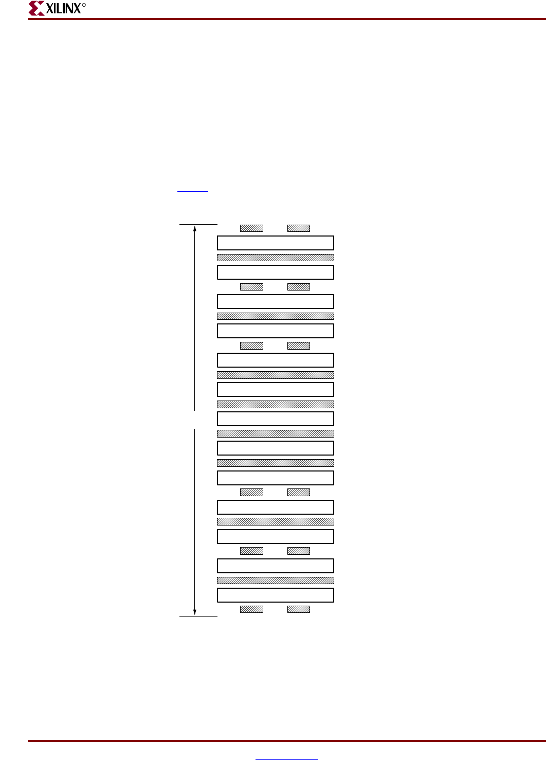
uses Polyclad 370HR material for lead-free assembly. Figure 3-11 shows a stack-up
diagram of the ML561 Revision A PCB.
Refer to UG203, Virtex-5 PCB Designer’s Guide for more information on the PCB design
using Virtex-5 devices.
Figure 3-11: ML561 Revision A PCB Stack-Up
73.90 ±7 mils
UG199_c3_11_102407
1.0 oz, TOP, Z0 = 50Ω, width = 6 mils
3.8 mils, Er = 4.4
1.0 oz, 02_GND1
4 mils, Er = 4.4
0.5 oz, 03_INR1, Z0 = 50Ω, width = 4.5 mils
5.3 mils, Er = 4.4
1.0 oz, 04_PWR1
8 mils, Er = 4.4
0.5 oz, 05_INR2, Z0 = 50Ω, width = 4.5 mils
3.2 mils, Er = 4.4
1.0 oz, 06_GND2
3 mils, Er = 4.4
1.0 oz, 07_PWR2
3.3 mils, Er = 4.4
1.0 oz, 08_PWR3
3 mils, Er = 4.4
1.0 oz, 09_GND3
3.2 mils, Er = 4.4
0.5 oz, 10_INR5, Z0 = 50Ω, width = 4.5 mils
8 mils, Er = 4.4
1.0 oz, 11_PWR4
5.3 mils, Er = 4.4
0.5 oz, 12_INR6, Z0 = 50Ω, width = 4.5 mils
4 mils, Er = 4.4
1.0 oz, 13_GND4
3.8 mils, Er = 4.4
1.0 oz, BOTTOM, Z0 = 50Ω, width = 6 mils
38 www.xilinx.com Virtex-5 FPGA ML561 User Guide
UG199 (v1.2) April 19, 2008
Chapter 3: Hardware Description
R
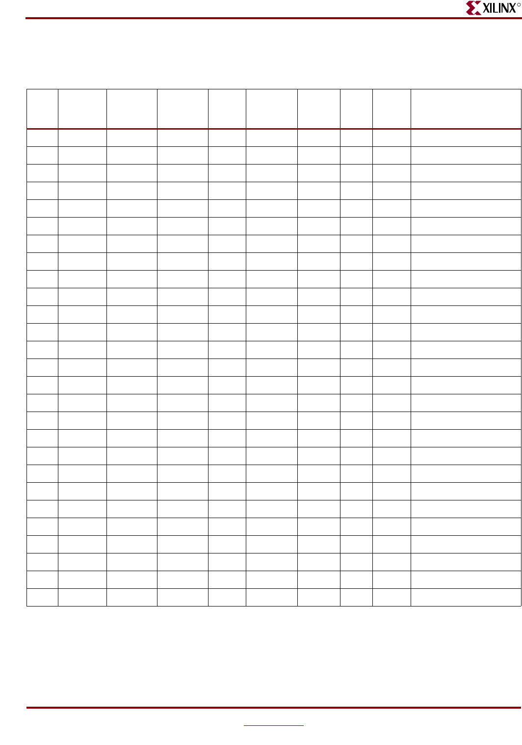
Table 3-19 shows the details of the dielectric material and construction for each layer and
the controlled impedance values for the signal layers.
Table 3-19: ML561 Revision A PCB Controlled Impedance
Seq # Layer
Name Type Usage
Cu
Weight
(oz.)
Substrate
Thickness
(mils)
Er
Test
Width
(mils)
Z0
(ohms) Comment
1 TOP Metal Signal 1.0 <Auto> 6 50 ±5 Microstrip Signal Top
2 Dielectric Substrate 3.8 4.4
3 02_GND1 Metal Plane 1.0 <Auto> Ground Plane #1
4 Dielectric Substrate 4 4.4
5 03_INR1 Metal Signal 0.5 <Auto> 4.5 50 ±5 Stripline Signal - Inner #1
6 Dielectric Substrate 5.3 4.4
7 04_PWR1 Metal Plane 1.0 <Auto> Split Power Plane #1
8 Dielectric Substrate 8 4.4
9 05_INR2 Metal Signal 0.5 <Auto> 4.5 50 ±5 Stripline Signal - Inner #2
10 Dielectric Substrate 3.2 4.4
11 06_GND2 Metal Plane 1.0 <Auto> Ground Plane #2
12 Dielectric Substrate 3 4.4
13 07_PWR2 Metal Plane 1.0 <Auto> Split Power Plane #2
14 Dielectric Substrate 3.3 4.4
15 08_PWR3 Metal Plane 1.0 <Auto> Split Power Plane #3
16 Dielectric Substrate 3 4.4
17 09_GND3 Metal Plane 1.0 <Auto> Ground Plane #3
18 Dielectric Substrate 3.2 4.4
19 10_INR5 Metal Signal 0.5 <Auto> 4.5 50 ±5 Stripline Signal - Inner #3
20 Dielectric Substrate 8 4.4
21 11_PWR4 Metal Plane 1.0 <Auto> Split Power Plane #4
22 Dielectric Substrate 5.3 4.4
23 12_INR6 Metal Signal 0.5 <Auto> 4.5 50 ±5 Stripline Signal - Inner #4
24 Dielectric Substrate 4 4.4
25 13_GND4 Metal Plane 1.0 <Auto> Ground Plane #4
26 Dielectric Substrate 3.8 4.4
27 BOTTOM Metal Signal 1.0 <Auto> 6 50 ±5 Microstrip Signal Bottom
Virtex-5 FPGA ML561 User Guide www.xilinx.com 39
UG199 (v1.2) April 19, 2008
R
Chapter 4
Electrical Requirements
This chapter provides the electrical requirements for the Virtex-5 FPGA ML561
Development Board. It contains the following sections:
•“Power Consumption”
•“FPGA Internal Power Budget”
Power Consumption
Table 4-1 lists the operating voltages, maximum currents, and power consumption used by
the ML561 board devices. The Virtex-5 FPGA ML561 Development Board has provisions
for two power inputs: a 5V power supply and a 12V power supply. The maximum rating of
a commercially available 5V power supply is limited to 8A, or a 40W maximum capacity.
This power supply is similar to the 5V brick used for previous memory tool kits, for
example, ML461. This tool kit expects the Virtex-5 FPGA ML561 Development Board to
exercise only one external memory interface at a time. In this case, the total power
consumption of the board stays within the 40W limit.
As shown in Table 4-1, if all three FPGA devices and their associated memory devices are
activated simultaneously, then the total power consumption is approximately 57W, which
exceeds the 40W capacity of the 5V power brick. So an alternate 12V power input jack (J23)
is provided on the Virtex-5 FPGA ML561 Development Board to hook up a 12V power
brick, for example, CUI DTS120500U with a 60W capacity. The 12V is converted to 5V
using the TI PTH12010WAS power module (VR11), which can supply up to 12A of current
at 5V, or a 60W capacity.
40 www.xilinx.com Virtex-5 FPGA ML561 User Guide
UG199 (v1.2) April 19, 2008
Chapter 4: Electrical Requirements
R
Table 4-1: ML561 Power Consumption
Device Description Quantity Voltage (V) Current
(mA)
Power
(W) Source
Total Available Power
5V Power Supply 1 5.0 8000 40.0 Bellus Power SPD-050-5
12V Power Supply 1 12.0 5000 60.0 CUI DTS120500U
Power Consumed
DDR400 Component Interface
XC5VLX50T-FFG1136:
FPGA #1 (DDR400)
1 1.0, 2.5, 2.6 1887 3.7 Xilinx Power Estimator
DDR x16 Memory 2 2.6 210 1.1 Micron DDR Component Data Sheet
DDR Comp VTT Termination 60 1.2 16 1.2 All signals. ±608 mV swing around VTT
DDR2 Component Interface
XC5VLX50T-FFG1136:
FPGA #1 (DDR2) 11.0, 1.8[S],
2.5 1991 3.1 Xilinx Power Estimator
DDR2 x16 Memory 2 1.8 250 0.9 Micron DDR2 Component Data Sheet
DDR2 Comp VTT Termination 25 1.2 16 0.5 Addr/Cntl: ±603 mV swing around VTT
DDR2 DIMM Interface
XC5VLX50T-FFG1136:
FPGA #2 (DDR2) 11.0, 1.8[S],
2.5 6420 10.2 Xilinx Power Estimator
DDR2 DIMM 2 1.8 1755 6.3 Micron DDR2 DIMM Data Sheet
DDR2 DIMM VTT Termination 160 1.2 16 3.1 All signals: ±603 mV swing around VTT
QDRII Memory Interface
XC5VLX50T-FFG1136:
FPGA #3 (QDRII) 11.0, 1.8[H],
1.8[S], 2.5 3917 6.3 Xilinx Power Estimator
QDRII Memory [H] 2 1.8 950 3.4 Samsung QDRII Data Sheet
QDRII VTT Termination 175 1.0 16 2.8 All signals. ±500 mV swing around VTT
RLDRAM II Memory Interface
XC5VLX50T-FFG1136:
FPGA #3 (RLDRAM II) 11.0, 1.8[H],
2.5 3069 4.5 Xilinx Power Estimator
RLDRAM II Memory 2 1.8 920 3.3 Micron RLDRAM II Data Sheet
RLDRAM II VTT Termination 60 1.0 16 1.0 All signals. ±500 mV swing around VTT
Miscellaneous Circuit
Clock Buffer 1 3.3 23 0.1 ICS8304 Data Sheet
Differential Clock Buffer 2 3.3 115 0.8 ICS853006 Data Sheet
System ACE Controller 1 3.3 200 0.7
DS080,
System ACE CompactFlash Solution
200 MHz Oscillator 1 2.5 30 0.1 Epson EG2121CA Data Sheet
33 MHz Oscillator 2 3.3 45 0.3 Epson SG-8002CA Data Sheet
Total Power Consumed 53.2
Virtex-5 FPGA ML561 User Guide www.xilinx.com 41
UG199 (v1.2) April 19, 2008
Power Consumption
R
Power Modules Capacity
VCCINT Power Plane (1.0V) 1 1.00 15000 15.0 TI PTH05010 15A Module Data Sheet
HSTL FPGA Power Plane (1.8V) 1 1.80 15000 27.0
HSTL Memory Power Plane (1.8V) 1 1.80 6000 10.8 TI PTH05000 6A Module Data Sheet
HSTL _VREF Power Plane (0.9V) 1 0.90 3000 2.7 Fairchild FN6555 Data Sheet
SSTL18 FPGA Power Plane (1.8V) 1 1.80 15000 27.0 TI PTH05010 15A Module Data Sheet
SSTL18 Memory Power Plane (1.8V) 1 1.80 6000 10.8 TI PTH05000 6A Module Data Sheet
SSTL18 _VREF Power Plane (0.9V) 1 0.90 3000 2.7 Fairchild FN6555 Data Sheet
SSTL2 FPGA Power Plane (2.6V) 1 2.60 15000 39.0 TI PTH05010 15A Module Data Sheet
SSTL2 Memory Power Plane (2.6V) 1 2.60 6000 15.6 TI PTH05000 6A Module Data Sheet
SSTL2 _VREF Power Plane (1.3V) 1 1.30 3000 3.9 Fairchild FN6555 Data Sheet
2.5V Power Plane 1 2.50 15000 37.5 TI PTH05010 15A Module Data Sheet
3.3V Power Plane 1 3.30 15000 49.5
12V-to-5V Converter 1 5.00 12000 60.0 TI PTH12010 12A Module Data Sheet
Notes:
1. [S] = 1.8V power for SSTL18 plane.
2. [H] = 1.8V power for HSTL18 plane.
Table 4-1: ML561 Power Consumption (Continued)
Device Description Quantity Voltage (V) Current
(mA)
Power
(W) Source
42 www.xilinx.com Virtex-5 FPGA ML561 User Guide
UG199 (v1.2) April 19, 2008
Chapter 4: Electrical Requirements
R
Table 4-2 lists the 12 different power planes on the Virtex-5 FPGA ML561 Development
Board. For the SSTL2, SSTL18, and HSTL power, separate power modules are
implemented for VCCO to FPGA, and VDD to memory, allowing for ease of power
measurement for the FPGAs. The power modules for VCCO inputs are implemented with
TI PTH05010 modules, which have provisions for ±5% voltage margining pins.
Each of the three Fairchild FN6555 Bus Terminator Regulators has two voltage outputs:
one each for VREF and VTT. The FN6555 regulator is a push-pull device rated at ± 3A for the
VTT output and 3 mA for the VREF output.
Because the VREF voltage is used by the FPGA and memory devices only as reference, the
power supply does not source any real current. Thus the 3 mA capacity for the VREF output
is considered sufficient.
The VTT voltage is guaranteed to within ± 20 mV of the VREF output by the FN6555
regulator. The minimum driver output voltage swing around VREF is specified for the
SSTL18, SSTL2, and HSTL I/O standards as:
•SSTL2: ± 608 mV
•SSTL18: ± 603 mV
•HSTL: ± 500 mV (for HSTL18)
For a given memory interface, the maximum number of single-ended (non-differential)
signals that might need to be pulled up or down at a time for QDRII is 144 data bits and
approximately 30 address and control signals. The differential pair signals offset for the
sink and source of current. With a continuous current capacity of 3A for the FN6555
regulator, the regulator can supply up to (3000 / 175) = 17 mA of current per signal. The
maximum drive strength for a driver is specified at 16 mA. For a 50Ω VTT termination, this
Table 4-2: Power Planes
Voltage Regulator Module (VRM) Part Power Plane VRM REFDES Stack-Up
Layer
TI PTH05010 15A Modules
VCCINT Power Plane (1.0V) VR6 Layer 4
SSTL18 FPGA Power Plane (1.8V) VR1 Layer 7
HSTL FPGA Power Plane (1.8V) VR10 Layer 8
VCCAUX Power Plane (2.5V) VR12 Layer 11
SSTL2 FPGA Power Plane (2.6V) VR9 Layer 8
TTL Power Plane (3.3V) VR13 Layer 11
TI PTH05000 6A Modules
SSTL18 Memory Power Plane (1.8V) VR4 Layer 7
HSTL Memory Power Plane (1.8V) VR14 Layer 8
SSTL2 Memory Power Plane (2.6V) VR2 Layer 8
Fairchild FN6555 3A Bus Term Regulators
(Separate outputs for VTT and VREF)
SSTL18_VREF Power Plane (0.9V) U14 Layer 8
SSTL18_VTT Power Plane (0.9V) Layer 8
HSTL_VREF Power Plane (0.9V) U42 Layer 7
HSTL_VTT Power Plane (0.9V) Layer 7
SSTL2_VREF Power Plane (1.3V) U2 Layer 7
SSTL2_VTT Power Plane (1.3V) Layer 7
Virtex-5 FPGA ML561 User Guide www.xilinx.com 43
UG199 (v1.2) April 19, 2008
Power Consumption
R
current can support a voltage swing of up to (16 mA * 50Ω) = 800 mV, which is sufficient to
meet the output voltage specifications for SSTL18, SSTL2, and HSTL18 I/O standards.
Table 4-3 separates the power consumption information from Table 4-1 according to the
nine TI power modules for the first set of nine power planes and the three Fairchild
regulators for the VTT power planes. The positive values in the Excess Power column of
Table 4-3 show that each of the 14 modules can supply the necessary power for the
corresponding power plane.
Table 4-3: ML561 Power Plane Capacities
Device Description Quantity Voltag e
(V)
Current
(mA)
Power
(W)
Excess
Power
(W)
Source
Total Available Power
5V Power Supply 1 5.0 8000 40.0 Bellus Power SPD-050-5
12V Power Supply 1 12.0 5000 60.0 CUI DTS120500U
Power Consumed by Power Plane
XC5VLX50T-FFG1136: FPGA #1
(DDR400, DDR2) 1 1.0 2289 2.3 Xilinx Power Estimator
XC5VLX50T-FFG1136: FPGA #2
(DDR2 DIMM) 1 1.0 1945 1.9 Xilinx Power Estimator
XC5VLX50T-FFG1136: FPGA #3
(QDRII and RLDRAM II) 1 1.0 2675 2.7 Xilinx Power Estimator
VCCINT Power Plane (1.0V) Capacity 1 1.0 15000 15.0 8.1 TI PTH05010 15A Module Data
Sheet
XC5VLX50T-FFG1136: FPGA #3
(QDRII and RLDRAM II) 1 1.8 3876 7.0 Xilinx Power Estimator
HSTL FPGA Power Plane (1.8V)
Capacity 1 1.8 15000 27.0 20.0 TI PTH05010 15A Module Data
Sheet
QDRII Memory [H] 2 1.8 950 3.4 Samsung QDRII Data Sheet
RLDRAM II Memory 2 1.8 920 3.3 Micron RLDRAM II Data Sheet
HSTL_Mem Power Plane (1.8V)
Capacity 1 1.8 6000 10.8 4.1 TI PTH05000 6A Module Data
Sheet
QDRII VTT Termination 175 1.0 16 2.8 All signals. ±500 mV swing
around VTT.
RLDRAM II VTT Termination 60 1.0 16 1.0 All signals. ±500 mV swing
around VTT.
HSTL _VREF Power Plane (0.9V) 1 0.9 3000 2.7 -0.1 Fairchild FN6555 Data Sheet
XC5VLX50T-FFG1136:
FPGA #1 (DDR2) 1 1.8 1011 1.8 Xilinx Power Estimator
XC5VLX50T-FFG1136:
FPGA #2 (DDR2 DIMM) 1 1.8 4258 7.7 Xilinx Power Estimator
44 www.xilinx.com Virtex-5 FPGA ML561 User Guide
UG199 (v1.2) April 19, 2008
Chapter 4: Electrical Requirements
R
SSTL18 FPGA Power Plane (1.8V)
Capacity 1 1.8 15000 27.0 17.5 TI PTH05010 15A Module Data
Sheet
DDR2 x16 Memory 2 1.8 250 0.9 Micron DDR2 Component Data
Sheet
DDR2 DIMM 2 1.8 1755 6.3 Micron DDR2 DIMM Data Sheet
SSTL18_Mem Power Plane (1.8V)
Capacity 1 1.8 6000 10.8 3.6 TI PTH05010 15A Module Data
Sheet
DDR2 Comp VTT Termination 25 1.2 16 0.5 Addr/Cntl: ±603 mV swing
around VTT
DDR2 DIMM VTT Termination 160 1.2 16 3.1 All signals: ±603 mV swing
around VTT
SSTL18 _VREF Power Plane (0.9V) 1 0.9 3000 2.7 -0.9 Fairchild FN6555 Data Sheet
XC5VLX50T-FFG1136: FPGA #1
(DDR400, DDR2) 1 2.5 609 1.5 Xilinx Power Estimator
XC5VLX50T-FFG1136: FPGA #2
(DDR2 DIMM) 1 2.5 218 0.5 Xilinx Power Estimator
XC5VLX50T-FFG1136: FPGA #3
(QDRII and RLDRAM II) 1 2.5 435 1.1 Xilinx Power Estimator
Differential Clock Buffer 2 2.5 115 0.8 ICS853006 Data Sheet
200 MHz Osc 1 2.5 30 0.1 Epson EG2121CA Data Sheet
2.5V Power Plane Capacity 1 2.5 15000 37.5 34.1 TI PTH05010 15A Module Data
Sheet
XC5VLX50T-FFG1136: FPGA #1
(DDR400) 1 2.6 950 2.5 Xilinx Power Estimator
SSTL2_FPGA Power Plane (2.6V)
Capacity 1 2.6 15000 39.0 36.5 TI PTH05010 15A Module Data
Sheet
DDR x16 Memory 2 2.6 210 1.1 Micron DDR Component Data
Sheet
SSTL2_Mem Power Plane (2.6V)
Capacity 1 2.6 6000 15.6 14.5 TI PTH05010 15A Module Data
Sheet
DDR Comp VTT Termination 60 1.2 16 1.2 All signals. ±608 mV swing
around VTT
SSTL2 _VREF Power Plane (1.3V) 1 1.3 3000 3.9 2.7 Fairchild FN6555 Data Sheet
Clock Buffer 1 3.3 23 0.1 ICS8304 Data Sheet
Table 4-3: ML561 Power Plane Capacities (Continued)
Device Description Quantity Voltag e
(V)
Current
(mA)
Power
(W)
Excess
Power
(W)
Source
Virtex-5 FPGA ML561 User Guide www.xilinx.com 45
UG199 (v1.2) April 19, 2008
Power Consumption
R
System ACE Controller 1 3.3 200 0.7 DS080, System ACE
CompactFlash Solution
33 MHz Oscillator 2 3.3 45 0.3 Epson SG-8002CA Data Sheet
3.3V Power Plane Capacity 1 3.3 15000 49.5 47.8 TI PTH05010 15A Module Data
Sheet
Total Power Consumed 53.2
12V-to-5V Power Module Capacity 1 5.0 12000 60.0 6.8 TI PTH12010 12A Module Data
Sheet
Notes:
1. [S] = 1.8V power for SSTL18 plane.
2. [H] = 1.8V power for HSTL18 plane.
Table 4-3: ML561 Power Plane Capacities (Continued)
Device Description Quantity Voltag e
(V)
Current
(mA)
Power
(W)
Excess
Power
(W)
Source
46 www.xilinx.com Virtex-5 FPGA ML561 User Guide
UG199 (v1.2) April 19, 2008
Chapter 4: Electrical Requirements
R
FPGA Internal Power Budget
Table 4-4 summarizes power consumption estimates by each of the three
XC5VLX50T-FFG1136 FPGAs on the Virtex-5 FPGA ML561 Development Board. This
estimate derives the FPGA utilization information from the respective map report of a fully
configured reference design.
Table 4-4: ML561 FPGA Power Estimate Summary
FPGA # FPGA #1 FPGA #2(1) FPGA #3
Interface DDR400 Comp
(DCI)
DDR2 Comp
(DCI)
DDR2 DIMM
(DCI) QDRII (DCI) RLDRAM II
(DCI)
I/O Standard SSTL_18 HSTL_18 HSTL_18
Total Power (W) 3.7 3.1 10.2 6.3 4.5
VCCINT (1.0V) mW 763 763 1945 1160 1515
VCCAUX (2.5V) mW 435 544 544 544 544
SSTL_18 VCCO (1.8V) mW 1819 7664
SSTL_2 VCCO (2.6V) mW 2469
HSTL_18 VCCO (1.8V) mW 4571 2406
I/O Frequency (MHz) 200 400 400 400 400
Fabric Frequency (MHz) 200 200 200 200 200
Number of Slices 1500 1500 5910 2750 1951
Number of Flip-flops 2000 2000 7352 2000 1800
Number of Shift Register LUTs 50 50 143 750 400
Number of Block RAMs 5 5 17 14 21
Number of DCMs 2 2 2 2 2
Inputs 10 10 10 90 13
Outputs 50 50 90 160 52
Bidirectionals 36 40 192 0 36
Ambient Temperature (°C) 25 25 25 25 25
Airflow (LFM) 0 0 250 250 0
Heat Sink (Theta-J) n/a n/a 5 5 n/a
Junction Temperature (°C) 67 60 78 58 76
Notes:
1. For DDR2 DIMMs as well as QDRII memory interfaces with DCI, an MD35E-10B heat sink is needed. A heat sink with Theta-J = 5.0
should be okay without airflow. See http://www.alphanovatech.com/c_md35e.html for the heat sink profile. A heat sink with
Theta-J = 5.0 might need airflow of 250 LFM.

Virtex-5 FPGA ML561 User Guide www.xilinx.com 47
UG199 (v1.2) April 19, 2008
R
Chapter 5
Signal Integrity Recommendations
Termination and Transmission Line Summaries
The following are common recommendations for the signal termination scheme to all
external memories implemented on the Virtex-5 FPGA ML561 Development Board:
•Single-ended signals: Simulation indicates that for a single-ended signal, there is no
significant performance difference for a signal with split termination of 100Ω + 100Ω
between VDD and GND versus the VTT termination of 50Ω to the VREF voltage.
Because the power consumption for the split termination is considerably higher than
the VTT termination for the SSTL2, SSTL18, and HSTL I/O standards, VTT termination
is recommended for single-ended signals on the board, such as data, address, and
control. For bidirectional single-ended signals (for example, DDR2 DQ), the VTT
termination is provided at both ends of the signal at the FPGA as well as at the
memory.
•Differential signals: For differential pair signals, a 100Ω differential termination is
provided between the two legs of the differential pair. This termination is placed
closest to the load. For bidirectional differential signals (for example, DDR2 DQS), the
differential SelectIO™ primitives in Virtex-5 FPGAs (for example,
DIFF_SSTL_II_18_DCI), account for the differential termination within the IOB. So
external differential termination is required only at the memory.
•Multiload signals: Address and control signals are driven by the FPGA, and they
have multiple loads. The termination is placed at the end of the trace after the last
load.
Table 5-1 through Table 5-5 summarize the specific termination schemes used on the
Virtex-5 FPGA ML561 Development Board for the following five different memory
interfaces. For each signal category, these tables include reference to the preliminary IBIS
simulation results(1).
1. DDR400 SDRAM Components (Table 5-1)
2. DDR2 SDRAM DIMM (Table 5-2)
3. DDR2 SDRAM Components (Table 5-3)
4. QDRII SRAM (Table 5-4)
5. RLDRAM II (Table 5-5)
1. Virtex-4 device IBIS models were used during the development of the ML561 board to understand the
expected signal integrity of the memory interface signals. When the Virtex-5 device IBIS models are available,
the results of post-layout IBIS simulations and characterization results will be reported.
48 www.xilinx.com Virtex-5 FPGA ML561 User Guide
UG199 (v1.2) April 19, 2008
Chapter 5: Signal Integrity Recommendations
R
Table 5-1: DDR400 SDRAM Component Terminations
Signal FPGA Driver Termination at FPGA Termination at Memory
Data (DQ) SSTL2_II_DCI No termination 50Ω pull-up to 1.3V
Data Strobe (DQS) SSTL2_II_DCI No termination 50Ω pull-up to 1.3V
Clock (CK, CK) SSTL2_II No termination 100Ω differential termination
between pair
Address (A, BA) SSTL2_II No termination 50Ω pull-up to 1.3V after the last
component
Control (RAS, CAS, WE, CS, DM, and
CKE)
SSTL2_II No termination 50Ω pull-up to 1.3V after the last
component
Table 5-2: DDR2 SDRAM DIMM Terminations
Signal FPGA Driver Termination at FPGA Termination at Memory
Data (DQ) SSTL18_II_DCI No termination No termination (use 75Ω ODT(1))
Data Strobe (DQS, DQS) DIFF_SSTL18_II_DCI No termination No termination (use 75Ω ODT)
Data Mask (DM) SSTL18_II No termination No termination (use 75Ω ODT)
6 Pairs of Clocks (CK, CK),
3 each per DIMM
SSTL18_II No termination No termination(2)
Address (A, BA) SSTL18_II No termination 50Ω pull-up to 0.9V after the second
DIMM
Control (RAS, CAS, WE,
CS, CKE, and others)
SSTL18_II No termination 50Ω pull-up to 0.9V after the second
DIMM
Notes:
1. Due to use of DCI I/O for DQ and DQS, these signals have parallel termination at the source during Write operations. Simulation
results show that use of a weaker 75Ω ODT instead of a matching 50Ω ODT setting gives better noise margin at the memory.
2. The DIMM already contains 120Ω differential termination. A 5 pF capacitive termination is provided on the board as per Micron
TN-47-01.
Table 5-3: DDR2 SDRAM Component Terminations
Signal FPGA Driver Termination at FPGA Termination at Memory
Data (DQ) SSTL18_II_DCI No termination No termination (use 75Ω ODT)
Data Strobe (DQS, DQS) DIFF_SSTL18_II_DCI No termination No termination (use 75Ω ODT)
Data Mask (DM) SSTL18_II No termination No termination (use 75Ω ODT)
Clock (CK, CK) SSTL18_II No termination 100Ω differential termination between
pair
Address (A, BA) SSTL18_II No termination 50Ω pull-up to 0.9V after the last
component
Control (RAS, CAS, WE, CS,
and CKE)
SSTL18_II No termination 50Ω pull-up to 0.9V after the last
component
Virtex-5 FPGA ML561 User Guide www.xilinx.com 49
UG199 (v1.2) April 19, 2008
Termination and Transmission Line Summaries
R
Table 5-4: QDRII SRAM Terminations
Signal FPGA Driver Termination at FPGA Termination at Memory
Write Data (D) HSTL_I_18 No termination 50Ω pull-up to 0.9V
Read Data (Q) HSTL_I_DCI_18 No termination No termination
Write Strobe (K, K) HSTL_I_18 No termination 50Ω pull-up to 0.9V
Read Strobe (CQ, CQ) HSTL_I_DCI_18 No termination No termination
Clock (CK, CK) HSTL_I_18 No termination 100Ω differential termination
between pair
Address (A, BA) HSTL_I_18 No termination 50Ω pull-up to 0.9V after the last
component
Control (RAS, CAS, WE,
CS, CKE, and BW)
HSTL_I_18 No termination 50Ω pull-up to 0.9V after the last
component
Table 5-5: RLDRAM II Terminations
Signal FPGA Driver Termination at FPGA Termination at Memory
Data (DQ for CIO) HSTL_II_DCI_18 No termination 50Ω pull-up to 0.9V
Data (Q for SIO) HSTL_I_DCI_18 No termination No termination
Write Data (D for SIO) HSTL_I_18 No termination 50Ω pull-up to 0.9V
Write Strobe (DK, DK) DIFF_HSTL_I_18 No termination 100Ω differential termination
between pair
Read Strobe (QK, QK) DIFF_HSTL_II_DCI_18 (for CIO)
DIFF_HSTL_I_DCI_18 (for SIO)
No termination No termination
Data Valid (QVLD) HSTL_II_DCI_18 (for CIO)
HSTL_I_DCI_18 (for SIO)
No termination No termination
Clock (CK, CK) DIFF_HSTL_I_18 No termination 100Ω differential termination
between pair
Address (A, BA) HSTL_I_18 No termination 50Ω pull-up to 0.9V after the last
component
Control (RAS, CAS, WE,
CS, and CKE)
HSTL_I_18 No termination 50Ω pull-up to 0.9V after the last
component

Virtex-5 FPGA ML561 User Guide www.xilinx.com 51
UG199 (v1.2) April 19, 2008
R
Chapter 6
Configuration
This chapter provides a brief description of the FPGA configuration methods used on the
Virtex-5 FPGA ML561 Development Board. This chapter contains the following sections:
•“Configuration Modes”
•“JTAG Chain”
•“JTAG Port”
•“Parallel IV Cable Port”
•“System ACE Interface”
Configuration Modes
The Virtex-5 FPGA ML561 Memory Interfaces Development Board includes several
options to configure the Virtex-5 FPGAs. The configuration modes are:
•System ACE mode
•JTAG mode
Table 6-1 shows the Virtex-5 FPGA configuration modes. The Master and Slave (Parallel)
SelectMAP configuration modes are not supported on the Virtex-5 FPGA ML561
Development Board. A separate 6-pin 3x2 header is provide for each FPGA to control the
Mode bits setting. The three headers are P27, P46, and P112 for FPGA #1, FPGA #2, and
FPGA #3, respectively. The even pins (# 2, 4, and 6) of the headers are tied to GND, and the
odd pins (# 1, 3, and 5) are connected to the respective Mode bit FPGA inputs (M0, M1, and
M2, respectively). A weak (4.7KΩ) pull-up is applied to each of these pins to set a logic '1'
by default.
Table 6-1: Configuration Modes
Mode XCONFIG
P72
JTAG
P114
Mode Jumpers(3,4)
5 -> 6
(M2)
3 -> 4
(M1)
1 -> 2
(M0)
Master Serial X(1) —(2) 000
Slave Serial X — 1 1 1
Master SelectMAP — — 0 1 1
Slave SelectMAP — — 1 1 0
JTAG — X 1 0 1
52 www.xilinx.com Virtex-5 FPGA ML561 User Guide
UG199 (v1.2) April 19, 2008
Chapter 6: Configuration
R
JTAG Chain
Four devices (the System ACE chip and three XC5VLX50T-FFG1136 FPGAs) are connected
via a JTAG chain on the Virtex-5 FPGA ML561 Development Board. The order of the four
devices in the JTAG chain is System ACE chip (U45), FPGA #1 (U7), FPGA #2 (U5), and
FPGA #3 (U34). The DONE pin of the FPGAs in the chain are tied together to a single LED
(D28). Each FPGA in the JTAG chain must be programmed for the board to be configured
properly. To program FPGAs in the JTAG chain that do not need functionality, a blank
design with no logic implementation can be used to compile to generate the corresponding
configuration bitstream.
Three different sources can be used to drive this JTAG chain:
•JTAG Port
•Xilinx Parallel IV Cable
•System ACE Controller
JTAG Port
The Virtex-5 FPGA ML561 Development Board provides a JTAG connector (P114) that can
be used to program the Virtex-5 FPGAs, and program and/or configure other JTAG
devices in the chain.
Parallel IV Cable Port
The Virtex-5 FPGA ML561 Development Board provides a Parallel IV Cable connector
(P64) to configure the Virtex-5 FPGAs and program JTAG devices located in the JTAG
chain.
System ACE Interface
The Virtex-5 FPGA ML561 Development Board provides a System ACE interface to
configure the Virtex-5 FPGA. The interface also gives software designers the ability to run
code (for soft processor IP within the FPGA) from removable CompactFlash cards.
Refer to the DS080, System ACE CompactFlash Solution for detailed information on creating
System ACE compatible ACE files, formatting the CompactFlash card, and storing
multiple design images.
System ACE CF Card — — 1 1 1
Notes:
1. X = Supported.
2. — = Not applicable.
3. Corresponding jumper position is Closed.
4. Corresponding jumper position is Open.
Table 6-1: Configuration Modes (Continued)
Mode XCONFIG
P72
JTAG
P114
Mode Jumpers(3,4)
5 -> 6
(M2)
3 -> 4
(M1)
1 -> 2
(M0)
Virtex-5 FPGA ML561 User Guide www.xilinx.com 53
UG199 (v1.2) April 19, 2008
System ACE Interface
R
Table 6-2 shows the System ACE interface signal names, descriptions, and pin
assignments.
Table 6-2: System ACE Interface Signal Descriptions
System ACE Pin Number Signal Name
70 SYSACE_MPA0
69 SYSACE_MPA1
68 SYSACE_MPA2
67 SYSACE_MPA3
45 SYSACE_MPA4
44 SYSACE_MPA5
43 SYSACE_MPA6
66 SYSACE_MPD0
65 SYSACE_MPD1
63 SYSACE_MPD2
62 SYSACE_MPD3
61 SYSACE_MPD4
60 SYSACE_MPD5
59 SYSACE_MPD6
58 SYSACE_MPD7
77 SYSACE_CTRL0/MPOE
76 SYSACE_CTRL1/MPWE
42 SYSACE_CTRL2/MPCE
41 SYSACE_CTRL3/MPIRQ
39 SYSACE_CTRL4/MPBRDY
93 SYSACE_CLK


Virtex-5 FPGA ML561 User Guide www.xilinx.com 55
UG199 (v1.2) April 19, 2008
R
Chapter 7
ML561 Hardware-Simulation
Correlation
This chapter contains the following sections:
•“Introduction”
•“Test Setup”
•“Signal Integrity Correlation Results”
•“Summary and Recommendations”
•“How to Generate a User-Specific FPGA IBIS Model”
Introduction
Signal integrity (SI) simulation is a very powerful tool that predicts the quality of signal at
the receiver. The quality of signal at the I/O buffer of the receiver device is most important
to the system designer. The observation point is buried within the IC device and is not
accessible for attaching a physical probe. This signal can only be simulated. It cannot be
measured on the hardware with an oscilloscope.
Signals can only be measured on hardware at the via probe points of a printed circuit board
(PCB) near the receiver device. For a high level of confidence in the SI simulation results, it
is necessary to develop and validate the simulation model to get a good correlation with
the hardware measurements at the probe points. When the correlation is obtained, the
same simulation model is used to extrapolate and accurately predict the signal quality at
the I/O buffer of the receiver device for the two significant corner driver conditions: slow-
weak and fast-strong.
The Virtex-5 FPGA ML561 Development Board implements five different memory
interfaces:
•32-bit DDR2 component
•144-bit DDR2 DIMM
•72-bit QDRII SRAM
•32-bit DDR component
•36-bit RLDRAM II
Each of these interfaces consists address, control, clock, data, and strobe signals. The
ML561 board has over 500 unique signals.
DDR2 SDRAMs and QDRII SRAM represent the large majority of Virtex-5 FPGA memory
applications. The dual data rate (DDR) data bits are the most critical signals to analyze.
This chapter presents SI analysis for only six representative data bit signals. The procedure

56 www.xilinx.com Virtex-5 FPGA ML561 User Guide
UG199 (v1.2) April 19, 2008
Chapter 7: ML561 Hardware-Simulation Correlation
R
illustrated here for these signals can be easily adopted to perform SI analysis for any other
memory interface signal on the ML561 board.
This chapter presents the SI results for the following six data bit signals:
•DDR2 component DQ bit (DDR2_DQ_BY2_B3) for write operations
•DDR2 component DQ bit (DDR2_DQ_BY2_B3) for read operations
•DDR2 DIMM DQ bit (DDR2_DIMM_DQ_BY2_B3) for write operations
•DDR2 DIMM DQ bit (DDR2_DIMM_DQ_BY2_B3) for read operations
•QDRII D bit (QDR2_D_BY0_B5) for write operations
•QDRII Q bit (QDR2_Q_BY0_B5) for read operations
Test Setup
Hardware measurements were performed for the six specific signal nets, and then signal
integrity (SI) simulations were performed for correlation and extrapolation. The test setup
consisted of the following hardware equipment, simulation software tools, the stimulus
test pattern, and test criteria for determining the quality of signals. The test bench is
designed so that the test pattern is applied only to the signal under test, and all other data
bits to the same memory interface are kept in a quiet Low state. This setup ensures that the
hardware measurement is not altered due to any simultaneous switching output (SSO)
effect.
•Hardware measurement equipment
♦Agilent DSO80604B 6 GHz oscilloscope
♦Agilent 1131A 3.5 GHz Infiniimax probe amplifier
♦Agilent E2675A (Differential browser) or E2677A (Differential solder-in probe) or
N5425A (ZIF probe)
♦Virtex-5 FPGA ML561, Rev B2 board: S/N 103
♦SRS Model CG635 Synthesized Clock Generator for low jitter clock source
•Simulation software
♦Mentor Graphics HyperLynx EXT, Version 7.5 with LineSim and BoardSim
features
♦Xilinx Virtex-5 FPGA IBIS package file: ff1136_5vlx50t.pkg, Rev 1.0 dated
June 12, 2006
♦ML561, Rev B layout file: ML561_B_041706.hyp
♦Micron DDR2-667 IBIS model for output and ODT input
♦Micron PC2-5300 RDIMM IBIS model
♦Molex DDR2 DIMM socket specification (P/N 087705-1041)
♦Samsung QDRII HSTL 1.8V IBIS model
♦IBISWriter Utility of ISE software suite to create customized IBIS model of the
FPGA1 (U7) and FPGA3 (U34) devices on the ML561 board: Model files
ml561_fpga1_u7.ibs and ml561_fpga3_u34.ibs. (See “How to Generate a
User-Specific FPGA IBIS Model,” page 93 for steps on how to create a customized
IBIS model of Virtex-5 FPGA for your design.)
•Stimulus
Pseudo Random Bit Stream (PRBS) is accepted as the most effective test pattern to
measure the quality of data signals because, unlike the periodic signals like clock and
Virtex-5 FPGA ML561 User Guide www.xilinx.com 57
UG199 (v1.2) April 19, 2008
Test Setup
R
strobe, a random value can be applied to data bits from one cycle to another. A 63-bit
PRBS6(1) (PRBS of order 6) test pattern stimulus is used for this analysis. The value of
this PRBS6 string is 63’h03F5_66ED_2717_9461, that is:
63’b000001111110101011001101110110100100111000101111001010001100001.
The HyperLynx stimulus setup is for: a 2-sequence repeat, 10 bits skipped, 1 eye, and
0% jitter.
•Test criteria
Quality of a signal is measured in terms of the opening of the signal eye at the receiver
input for both the amplitude and the width. DDR2 SDRAM (Component and DIMM)
interfaces utilize the SSTL_18 I/O standard, and the QDRII SRAM interface utilizes
the HSTL 1.8V I/O standard. For each of these two I/O standards, the eye mask is
defined by the trapezoid enclosed by the following four voltage thresholds at the
receiver input:
♦VIH(ac)-min at the rising edge
♦VIH(dc)-min at the falling edge
♦VIL(dc)-max at the rising edge
♦VIL(ac)-max at the falling edge
Refer to Figure 7-1 for the definition of voltage levels with regard to the trapezoidal
eye mask. Refer to “Terminology,” page 9 for definitions of the voltage thresholds.
Because the HyperLynx SI simulation software does not support a trapezoidal mask
definition, two separate triangular masks for VIH and VIL are defined, as shown in
Figure 7-2, such that the third vertex of triangle falls on the VREF axis.
1. A maximal-length PRBS test sequence of order n generates all (2n – 1), n-bit combinations of test sequences
(except all 0s). Thus the test sequence contains one n-bit long consecutive string of 1s and two (n-1)-bit long
consecutive strings of 0s. With the PRBS6 test pattern, at the highest test frequency of 333 MHz (that is, the bit
time is 1.5 ns), measurements in this setup result in a maximum settling time of (1.5 ns * 5) = 7.5 ns for a logic
Low, and a maximum settling time of (1.5 ns * 6) = 9 ns for a logic High. 7.5 ns is sufficient time for the test
signal to reach a steady state before the next transition. Thus a PRBS test pattern of higher order, such as 7 or
9, does not change the eye pattern, as proven by sample simulation of one test signal with PRBS6, PRBS7, and
PRBS9 stimuli.
Figure 7-1: Single Trapezoid Eye Mask Definition
VOH(dc)
VOL(dc)
VOH(ac)
VOL(ac)
UG199_c7_01_062707
VIH(ac)
VIL(ac)
VIH(dc)
VIL(dc)
VDDQ
VSS
VREF
58 www.xilinx.com Virtex-5 FPGA ML561 User Guide
UG199 (v1.2) April 19, 2008
Chapter 7: ML561 Hardware-Simulation Correlation
R
♦DDR2 mask (for nominal VDDQ = 1.8V and VREF = 0.9V):
-VIH(ac)-min = VREF + 200 mV = 1.1V
-VIH(dc)-min = VREF + 125 mV = 1.025V
-VIL(ac)-max = VREF – 200 mV = 0.7V
-VIL(dc)-max = VREF – 125 mV = 0.775V
♦QDRII mask (for nominal values of VDDQ = 1.8V and VREF = 0.9V):
-VIH(ac)-min = VREF + 200 mV = 1.1V
-VIH(dc)-min = VREF + 100 mV = 1.0V
-VIL(ac)-max = VREF – 200 mV = 0.7V
-VIL(dc)-max = VREF – 100 mV = 0.8V
Signal Integrity Correlation Results
This section presents SI results for each of the six chosen memory signals on the ML561
board. The following information is presented for each memory signal:
•A post-layout IBIS schematics of the signal under test
•A description of the major circuit elements(1) of this signal
•A summary of four SI results: hardware measurement, correlation simulation, slow-
weak corner driver simulation extrapolation, and fast-strong corner driver simulation
extrapolation
•A set of eight figures showing eye and waveform scope shots for each of the four SI
results mentioned in the bulleted list in the previous section
For an explanation of the different terms used to present these results, refer to
“Terminology,” page 9 for some definitions and routing terminologies.
Figure 7-2: Two Triangular Eye Mask Definitions for VIH and VIL
VOH(dc)
VOL(dc)
VOH(ac)
VOL(ac)
UG199_c7_02_062707
VIH(ac)
VIL(ac)
VIH(dc)
VIL(dc)
VDDQ
VSS
VREF
1. With regard to transmission line impedance, Table 3-19 in the “Board Design Considerations” section lists
controlled impedance values of all routing layers. The design goal for the ML561 board is to keep the
characteristic impedance for all routing layers as close to 50Ω as possible. Manufacturing tolerance is usually
±10%. The characteristic impedance of DIMM PCB is derived from the Micron DIMM layout file.
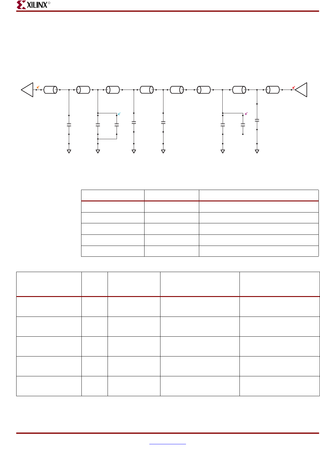
Virtex-5 FPGA ML561 User Guide www.xilinx.com 59
UG199 (v1.2) April 19, 2008
Signal Integrity Correlation Results
R
DDR2 Component Write Operation
This subsection shows the test results for the DDR2_DQ_BY2_B3 signal from FPGA1 (U7)
to the DDR2 memory component (U12) measured at 333 MHz (667 Mb/s), where the unit
interval (UI) = 1.5 ns.
Figure 7-3: Post-Layout IBIS Schematics of DDR2 Component Write Data Bit (DDR2_DQ_BY2_B3)
UG199_c7_03_071907
MT47H32M16CC_…
DQ11
U12.D3
TL2 TL3 TL8 TL9 TL5
U7.P25
DDR2_D…
DDR2_D…
DDR2_D…
DDR2_D…
DDR2_D… C7
C9
DDR2_D…
28.5 ohms
3.579 ps
0.022 in
DDR2_DQ_BY2_B3
71.0 ohms
27.482 ps
AutoPadstk_3
22.9 fF 22.9 fF 500.0 fF 58.1 fF 140.8 fF
365.6 fF
49.0 ohms
24.721 ps
0.164 in
DDR2_DQ_BY2_B3
58.3 ohms
25.244 ps
AutoPadstk_19
21.2 ohms
1.000 ps
AutoPadstk_3
49.1 ohms
47.132 ps
0.302 in
DDR2_DQ_BY2_B3
49.1 ohms
445.560 ps
2.852 in
DDR2_DQ_BY2_B3
28.5 ohms
4.473 ps
0.028 in
DDR2_DQ_BY2_B3
Virtex-5 FPGA
DDR2_DQ_BY2_B3
TL4 TL6 TL1
500.0 fF
22.9 fF
Table 7-1: Circuit Elements of DDR2 Component Write Data Bit
(DDR2_DQ_BY2_B3)
Element Designation Description
Driver U7.P25 FPGA SSTL18_II_DCI_O
Receiver U12.D3 DDR2 Memory, 75 Ω ODT
Probe Point C9 Via under the memory device
PCB Termination None ODT75 at load
Trace Length TL 2, 4, 9, 6, 1 3.37 inches
Table 7-2: DDR2 Component Write Operation Correlation Results
Measurement DVW(1)
(%UI)
ISI
(% UI)
Noise Margin
(VIH, + VIL) = Total
(% of VREF)
Overshoot / Undershoot
Margin
(% of VREF)
Hardware at probe
point
1.18 ns
(78.7%)
(80 + 80) = 160 ps
(10.7%)
(274 + 384) = 658 mV
(73.1%)
(550 + 470) = 1020 mV
(113.3%)
Simulation correlation
slow-weak corner
1.22 ns
(81.3%)
(77 + 36) = 113 ps
(7.5%)
(294 + 266) = 560 mV
(62.2%)
(461 + 490) = 951 mV
(105.7%)
Correlation Delta:
HW vs. Simulation
40 ps
(2.6%)
47 ps
(3.2%)
98 mV
(10.9%)
69 mV
(7.6%)
Extrapolation at IOB
slow-weak corner
1.27 ns
(84%)
(91 + 36) = 127 ps
(8.5%)
(300 + 270) = 570 mV
(63.3%)
(469 + 501) = 970 mV
(107.8%)
Extrapolation at IOB
fast-strong corner
1.39 ns
(92%)
(34 + 20) = 54 ps
(3.7%)
(406 + 351) = 757 mV
(84.1%)
(304 + 381) = 685 mV
(76.1%)
Notes:
1. DVW = Data Valid Window, ISI = Inter-Symbol Interference
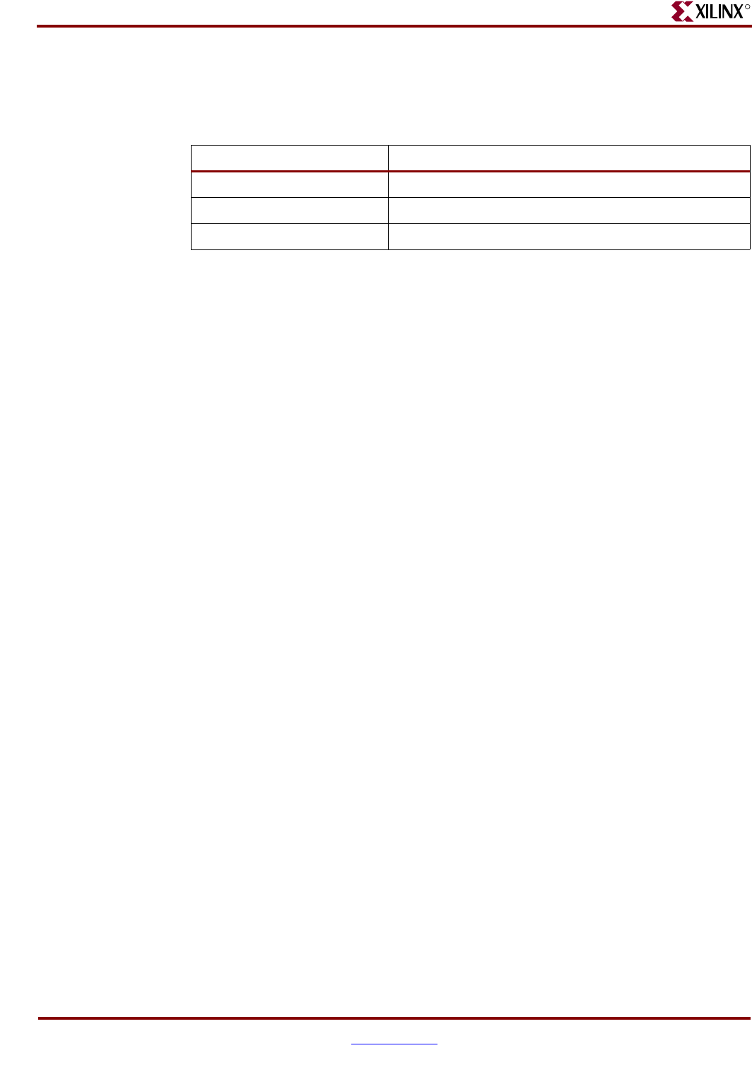
60 www.xilinx.com Virtex-5 FPGA ML561 User Guide
UG199 (v1.2) April 19, 2008
Chapter 7: ML561 Hardware-Simulation Correlation
R
DDR2 DQ is a bidirectional signal. To perform hardware measurements for a Write
operation that is not interrupted by a Read response or a Refresh operation, the testbench
on FPGA1 is controlled by DIP switches (SW2) as indicated in Table 7-3.
Table 7-3: DIP[1:2] Settings
Setting Description
2’b00 or 2’b11 Normal alternating Write/Read sequence
2’b01 Write only, Refresh disabled
2’b10 Write once, then Read only, Refresh disabled
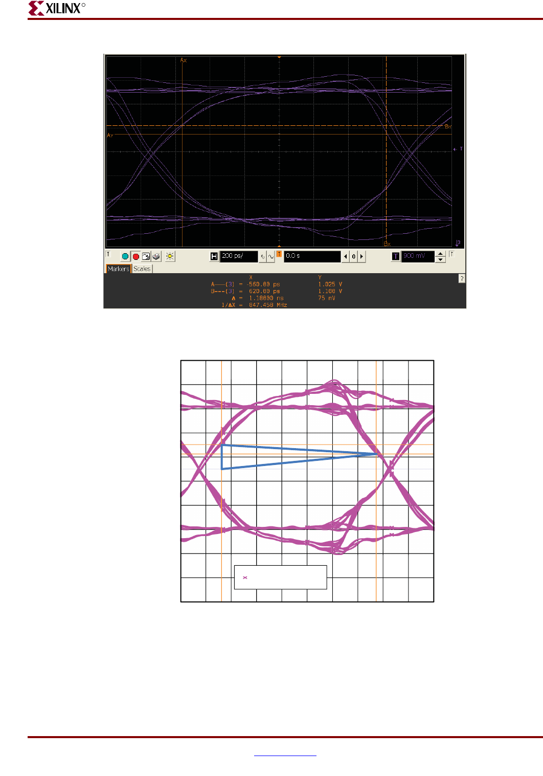
Virtex-5 FPGA ML561 User Guide www.xilinx.com 61
UG199 (v1.2) April 19, 2008
Signal Integrity Correlation Results
R
Figure 7-4: DDR2 Component Write HW Measurement - Eye Scope Shot at Probe Point (DDR2 Memory Via)
UG199_c7_04_071107
Figure 7-5: DDR2 Component Write Correlation - Eye Scope Shot at Probe Point (Slow Corner)
0.000 400.0 800.0 1200.0 1600.0
-200.0
0.000
200.0
400.0
600.0
800.0
1000.0
Voltage (mV)
1200.0
1400.0
1600.0
1800.0
Time (ps)
Probe 3:C9.1 (at pin)
UG199_c7_05_070907
♦333 MHz, Slow, PRBS6, 81.5% UI
♦Cursor 1: 1.1028V, 123.6 ps
♦Cursor 2: 1.0253V, 1.3458 ns
♦Delta Voltage = 77.5 mV, Delta Time = 1.2222 ns (81.5% UI)
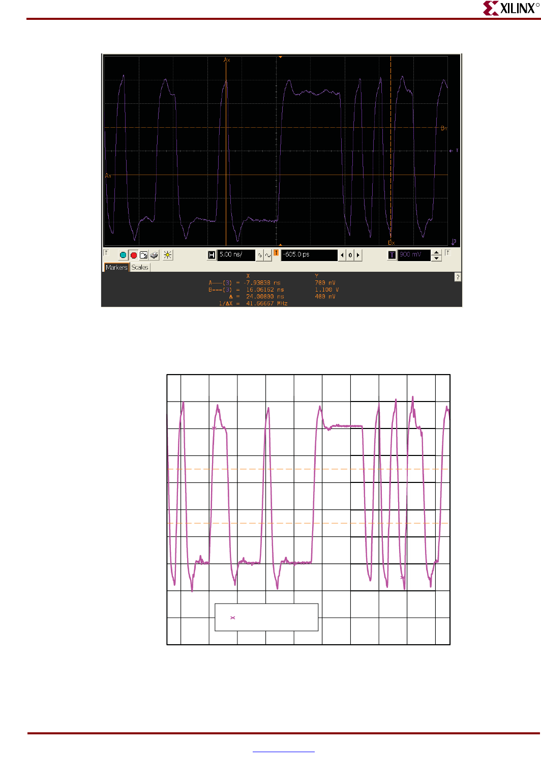
62 www.xilinx.com Virtex-5 FPGA ML561 User Guide
UG199 (v1.2) April 19, 2008
Chapter 7: ML561 Hardware-Simulation Correlation
R
Figure 7-6: DDR2 Component Write HW Measurement - Waveform Scope Shot at Probe Point
(DDR2 Memory Via)
UG199_c7_06_071107
Figure 7-7: DDR2 Component Write Correlation - Waveform Scope Shot at Probe Point (Slow Corner)
65.000 75.000 85.000 95.000 105.000
-200.0
Time (ns)
Voltage (mV)
0.000
200.0
400.0
600.0
800.0
1000.0
1200.0
1400.0
1600.0
1800.0
Probe 3:C9.1 (at pin)
UG199_c7_07_070907
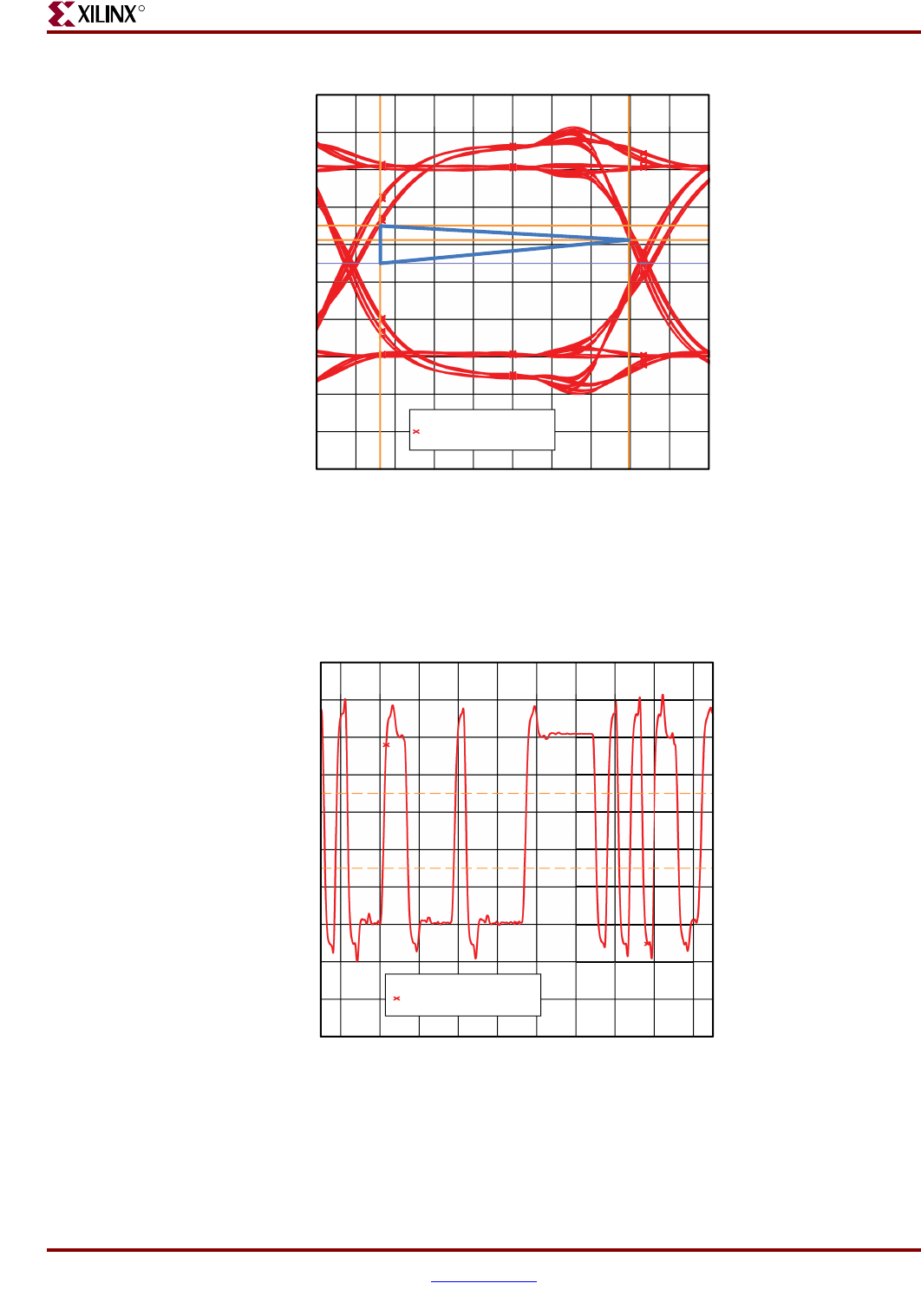
Virtex-5 FPGA ML561 User Guide www.xilinx.com 63
UG199 (v1.2) April 19, 2008
Signal Integrity Correlation Results
R
Figure 7-8: DDR2 Component Write Extrapolation - Eye Scope Shot at Receiver IOB (Slow Corner)
-200.0 200.0 600.0
Time (ps)
Voltage (mV)
1000.0 1400.0 1800.0
-200.0
0.000
200.0
400.0
600.0
800.0
1000.0
1200.0
1400.0
1600.0
1800.0
Probe 1:U12.D3 (at die)
UG199_c7_08_071007
♦333 MHz, Slow, PRBS6, 84.5% UI
♦Cursor 1: 1.1007V, 123.7 ps
♦Cursor 2: 1.0253V, 1.3921 ns
♦Delta Voltage = 75.4 mV, Delta Time = 1.2684 ns (84.5% UI)
Figure 7-9: DDR2 Component Write Extrapolation - Waveform Scope Shot at Receiver IOB (Slow Corner)
65.000 75.000 85.000 95.000 105.000
UG199_c7_09_071007
-200.0
Time (ns)
0.000
200.0
400.0
600.0
Voltage (mV)
800.0
1000.0
1200.0
1400.0
1600.0
1800.0
Probe 1:U12.D3 (at die)
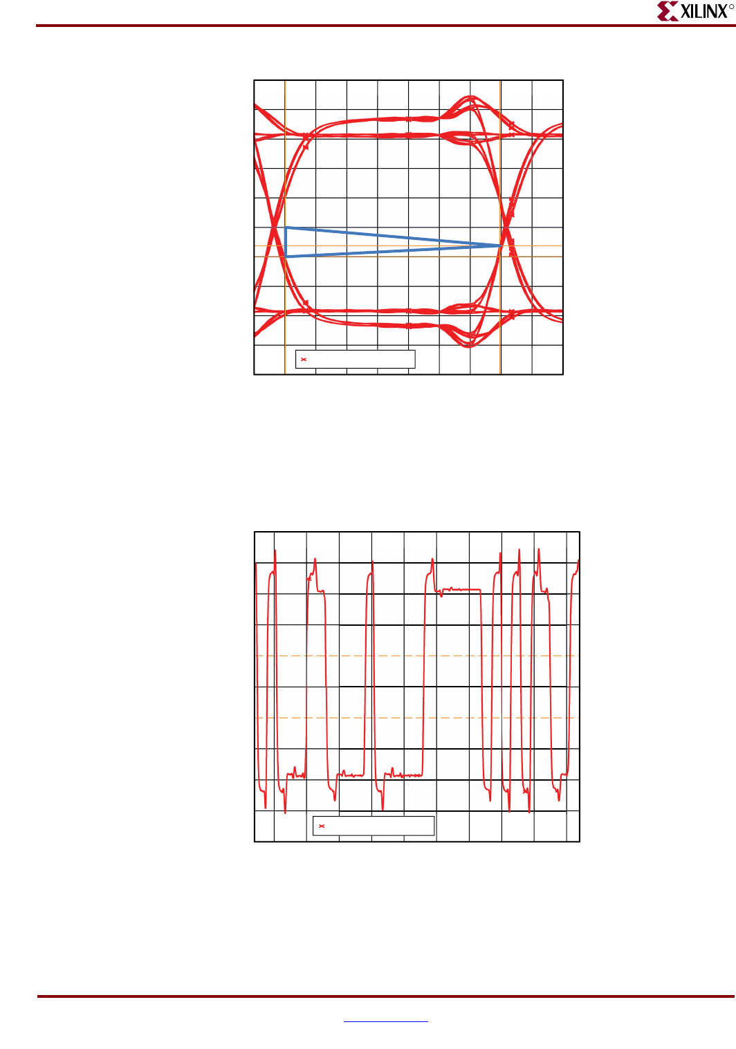
64 www.xilinx.com Virtex-5 FPGA ML561 User Guide
UG199 (v1.2) April 19, 2008
Chapter 7: ML561 Hardware-Simulation Correlation
R
Figure 7-10: DDR2 Component Write Extrapolation - Eye Scope Shot at Receiver IOB (Fast Corner)
UG199_c7_10_071007
-100.0
100.0
300.0
500.0
700.0
900.0
1100.0
1300.0
Voltage (mV)
1500.0
1700.0
1900.0
800.0 1200.0 1600.0
Time (ps)
2000.0 2400.0 2800.0
Probe 1:U12.D3 (at die)
♦333 MHz, Fast, PRBS6, 92.5% UI
♦Cursor 1: 701.2 mV, 1.0026 ns
♦Cursor 2: 774.6 mV, 2.3908 ns
♦Delta Voltage = 73.4 mV, Delta Time = 1.3883 ns (92.5% UI)
Figure 7-11: DDR2 Component Write Extrapolation - Waveform Scope Shot at Receiver IOB (Fast Corner)
65.000 75.000 85.000 95.000 105.000
UG199_c7_11_071007
-100.0
Time (ns)
100.0
300.0
500.0
700.0
Voltage (mV)
900.0
1100.0
1300.0
1500.0
1700.0
1900.0
Probe 1:U12.D3 (at die)
Virtex-5 FPGA ML561 User Guide www.xilinx.com 65
UG199 (v1.2) April 19, 2008
Signal Integrity Correlation Results
R
DDR2 Component Read Operation
This subsection shows the test results for the DDR2_DQ_BY2_B3 signal from the DDR2
memory component (U12) to FPGA1 (U7) measured at 333 MHz (667 Mb/s), where the
unit interval (UI) = 1.5 ns.
To perform hardware measurements for a Read operation that is not interrupted by a Write
or a Refresh operation, the testbench on FPGA1 is controlled by the following DIP switch
(SW2) setting:
•DIP[1:2] = 2’b10 – Write once, then Read only, Refresh disabled
Figure 7-12: Post-Layout IBIS Schematics of the DDR2 Component Read Data Bit (DDR2_DQ_BY2_B3)
49.0 ohms
24.721 ps
0.164 in
DDR2_DQ_BY2_B3
28.5 ohms
3.579 ps
0.022 in
DDR2_DQ_BY2_B3
MT47H64M8CB-3
DQ3
TL2 TL3 TL4 TL8 TL9 TL6 TL5 TL1 U7.P25
C7
C9
U12.D3
49.1 ohms
47.132 ps
0.302 in
DDR2_DQ_BY2_B3
58.3 ohms
25.244 ps
AutoPadstk_19
21.2 ohms
1.000 ps
AutoPadstk_3
71.0 ohms
27.482 ps
AutoPadstk_3
49.1 ohms
445.560 ps
2.852 in
DDR2_DQ_BY2_B3
28.5 ohms
4.473 ps
0.028 in
DDR2_DQ_BY2_B3
Virtex-5 FPGA
DDR2_DQ_BY2_B3
22.9 fF 22.9 fF 500.0 fF 58.1 fF 140.8 fF
DDR2_D… DDR2_D… DDR2_D… DDR2_D…
DDR2_D…
DDR2_D…
365.6 fF 500.0 fF
22.9 fF
UG199_c7_12_071907
Table 7-4: Circuit Elements of DDR2 Component Read Data Bit
(DDR2_DQ_BY2_B3)
Element Designation Description
Driver U12.D3 DDR2 Memory
Receiver U7.P25 FPGA SSTL18_II_DCI_I
Probe Point C7 Via under FPGA1
PCB Termination None DCI at receiver
Trace Length TL 2, 4, 9, 6, 1 3.37 inches
Table 7-5: DDR2 Component Read Operation Correlation Results
Measurement DVW (% UI) ISI
(% UI)
Noise Margin
(VIH + VIL) = Total
(% of VREF)
Overshoot /
Undershoot Margin
(% of VREF)
Hardware at probe point 1.28 ns
(85%)
(70 + 110) = 180 ps
(12%)
(423 + 416) = 839 mV
(83.1%)
(400 +400) = 800 mV
(79.1%)
Simulation correlation
slow-weak corner
1.28 ns
(85%)
(132 + 91) = 223 ps
(14.9%)
(406 +439) = 845 mV
(83.8%)
(279 +277) = 556 mV
(61.9%)
Correlation Delta:
HW vs. Simulation
0 ps
(0.0%)
43 ps
(2.9%)
6 mV
(0.7%)
244 mV
(17.2%)
Extrapolation at IOB
slow-weak corner
1.29 ns
(86%)
(96 + 82) = 178 ps
(11.9%)
(418 + 449) = 867 mV
(96.3%)
(304 +265) = 569 mV
(63.1%)
Extrapolation at IOB
fast-strong corner
1.32 ns
(88%)
(29 + 67) = 96 ps
(6.7%)
(455 +435) = 890 mV
(98.9%)
(167 +182) = 349 mV
(38.9%)
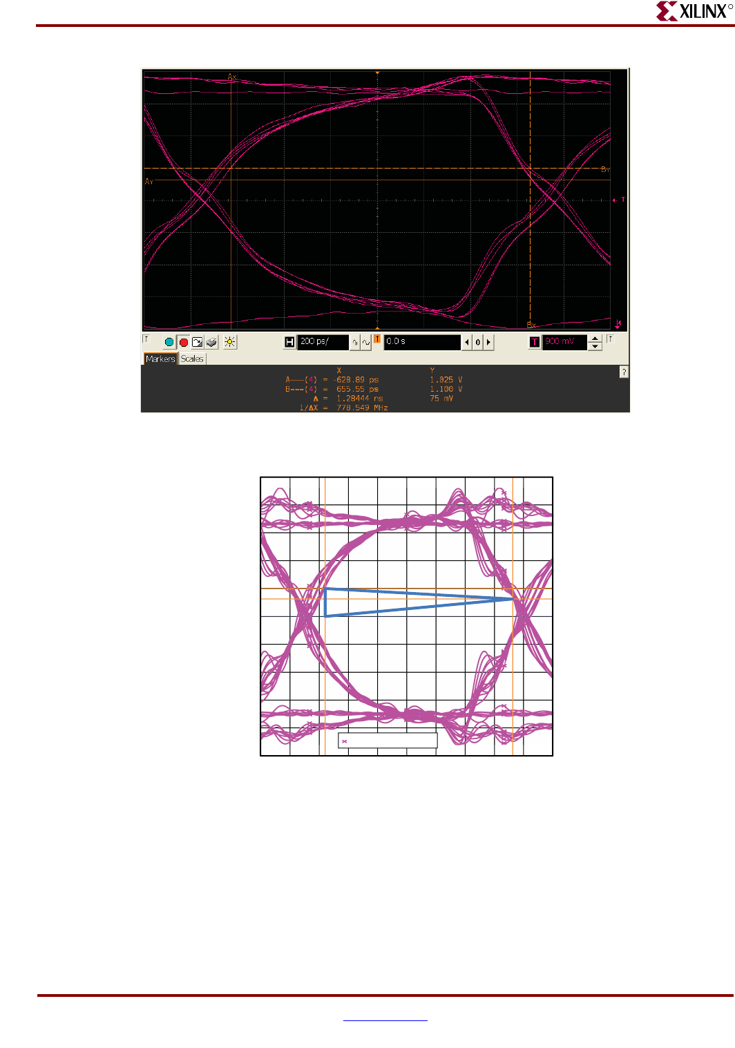
66 www.xilinx.com Virtex-5 FPGA ML561 User Guide
UG199 (v1.2) April 19, 2008
Chapter 7: ML561 Hardware-Simulation Correlation
R
Figure 7-13: DDR2 Component Read HW Measurement - Eye Scope Shot at Probe Point (FPGA1 Via)
UG199_c7_13_071107
Figure 7-14: DDR2 Component Read Correlation - Eye Scope Shot at Probe Point (Slow Corner)
800.0 1200.0 1600.0 2000.0 2400.0 2800.0
UG199_c7_14_071107
Time (ns)
Voltage (mV)
-100.0
100.0
300.0
500.0
700.0
900.0
1100.0
1300.0
1500.0
1700.0
1900.0
Probe 3:C7.1 (at pin)
♦333 MHz, Slow, PRBS6, 85.9% UI
♦Cursor 1: 697.1 mV, 1.2345 ns
♦Cursor 2: 774.6 mV, 2.5191 ns
♦Delta Voltage = 77.5 mV, Delta Time = 1.2846 ns (85.9% UI)
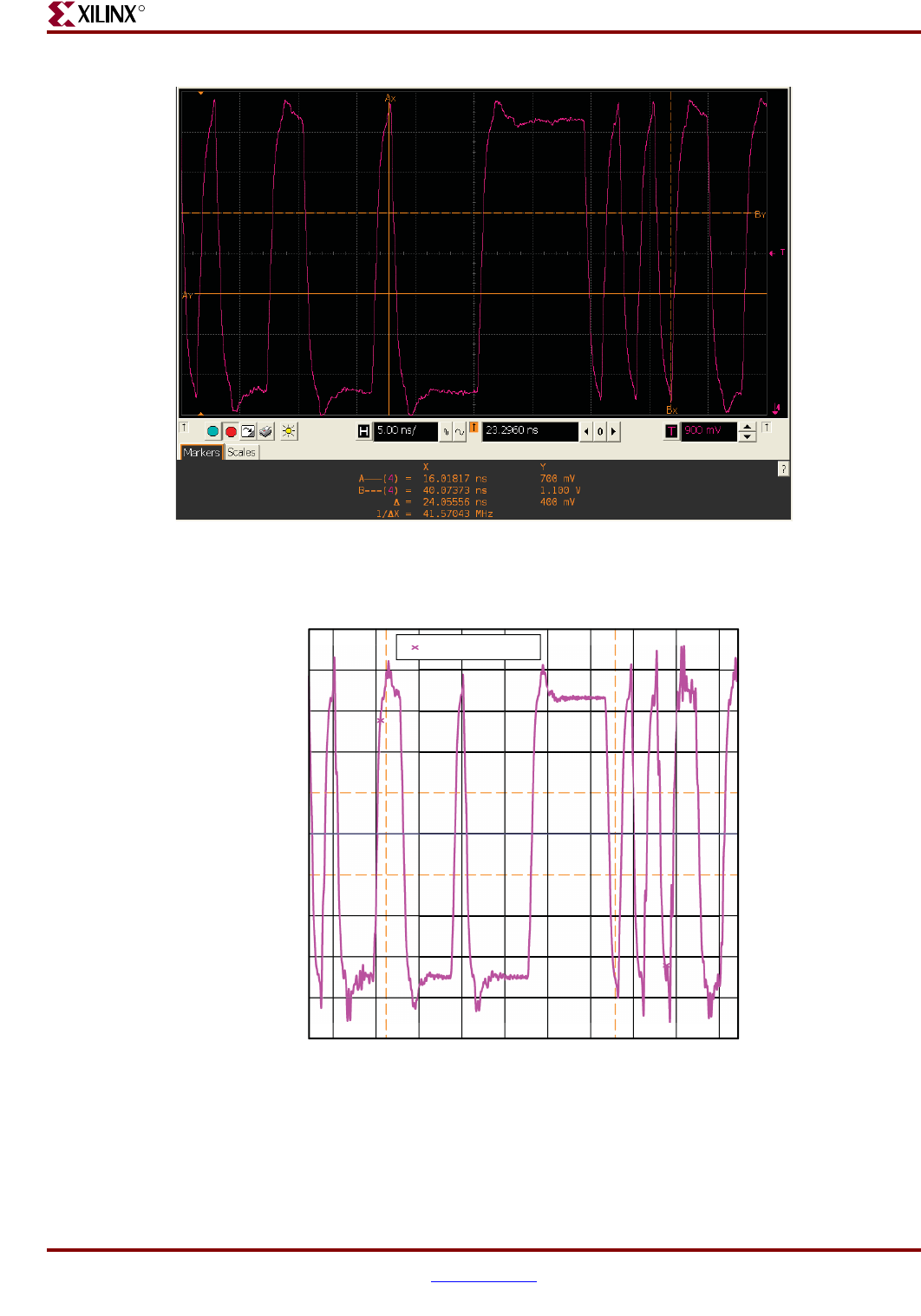
Virtex-5 FPGA ML561 User Guide www.xilinx.com 67
UG199 (v1.2) April 19, 2008
Signal Integrity Correlation Results
R
Figure 7-15: DDR2 Component Read HW Measurement - Waveform Scope Shot at Probe Point (FPGA1
Via)
UG199_c7_15_071107
Figure 7-16: DDR2 Component Read Correlation - Waveform Scope Shot at Probe Point (Slow Corner)
65.000 75.000 85.000 95.000 105.000
-100.0
100.0
300.0
500.0
700.0
900.0
1100.0
1300.0
1500.0
1700.0
1900.0
UG199_c7_16_071007
Time (ns)
Voltage (mV)
Probe 3:C7.1 (at pin)
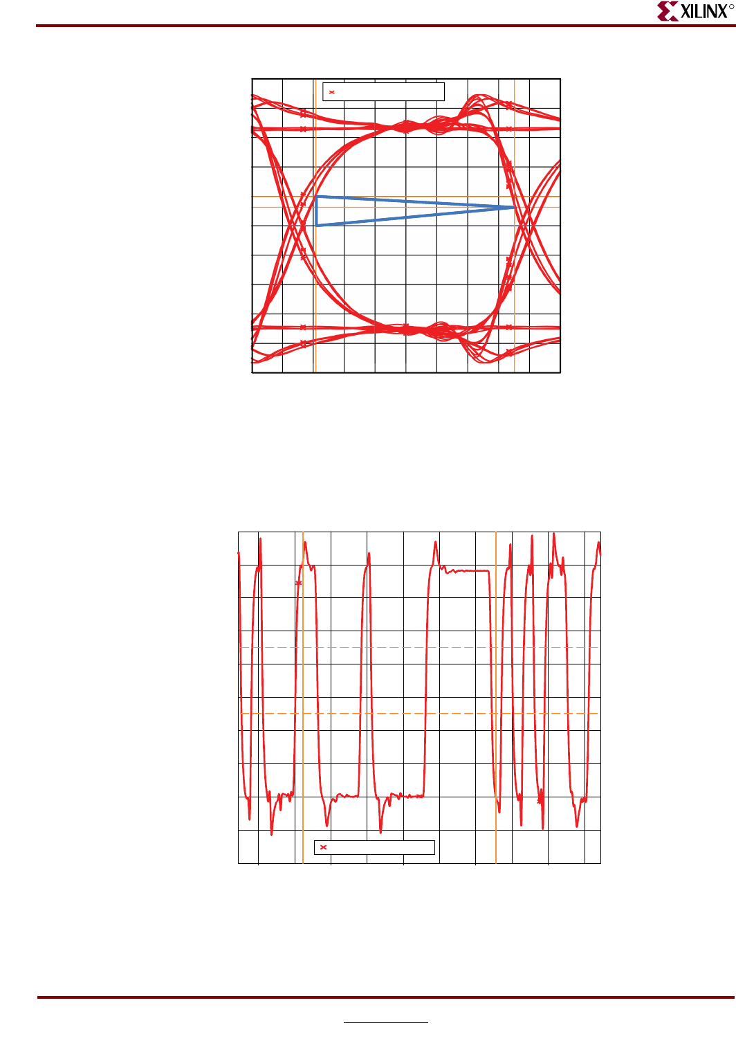
68 www.xilinx.com Virtex-5 FPGA ML561 User Guide
UG199 (v1.2) April 19, 2008
Chapter 7: ML561 Hardware-Simulation Correlation
R
Figure 7-17: DDR2 Component Read Extrapolation - Eye Scope Shot at Receiver IOB (Slow Corner)
800.0 1200.0 1600.0 2000.0 2400.0 2800.0
-100.0
100.0
300.0
500.0
700.0
900.0
1100.0
1300.0
1500.0
1700.0
1900.0
UG199_c7_17_071007
Time (ps)
Voltage (mV)
Probe 1:U7.P25 (at die)
♦333 MHz, Slow, PRBS6, 85.5% UI
♦Cursor 1: 1.0988V, 1.2170 ns
♦Cursor 2: 1.0254V, 2.5029 ns
♦Delta Voltage = 73.4 mV, Delta Time = 1.2859 ns (85.5% UI)
Figure 7-18: DDR2 Component Read Extrapolation - Waveform Scope Shot at Receiver IOB (Slow Corner)
-200.0
0.000
200.0
400.0
600.0
800.0
1000.0
1200.0
1400.0
1600.0
1800.0
65.000 75.000 85.000 95.000 105.000
Probe 1:U7.P25 (at die)
Voltage (mV)
Time (ns) UG199_c7_18_071007
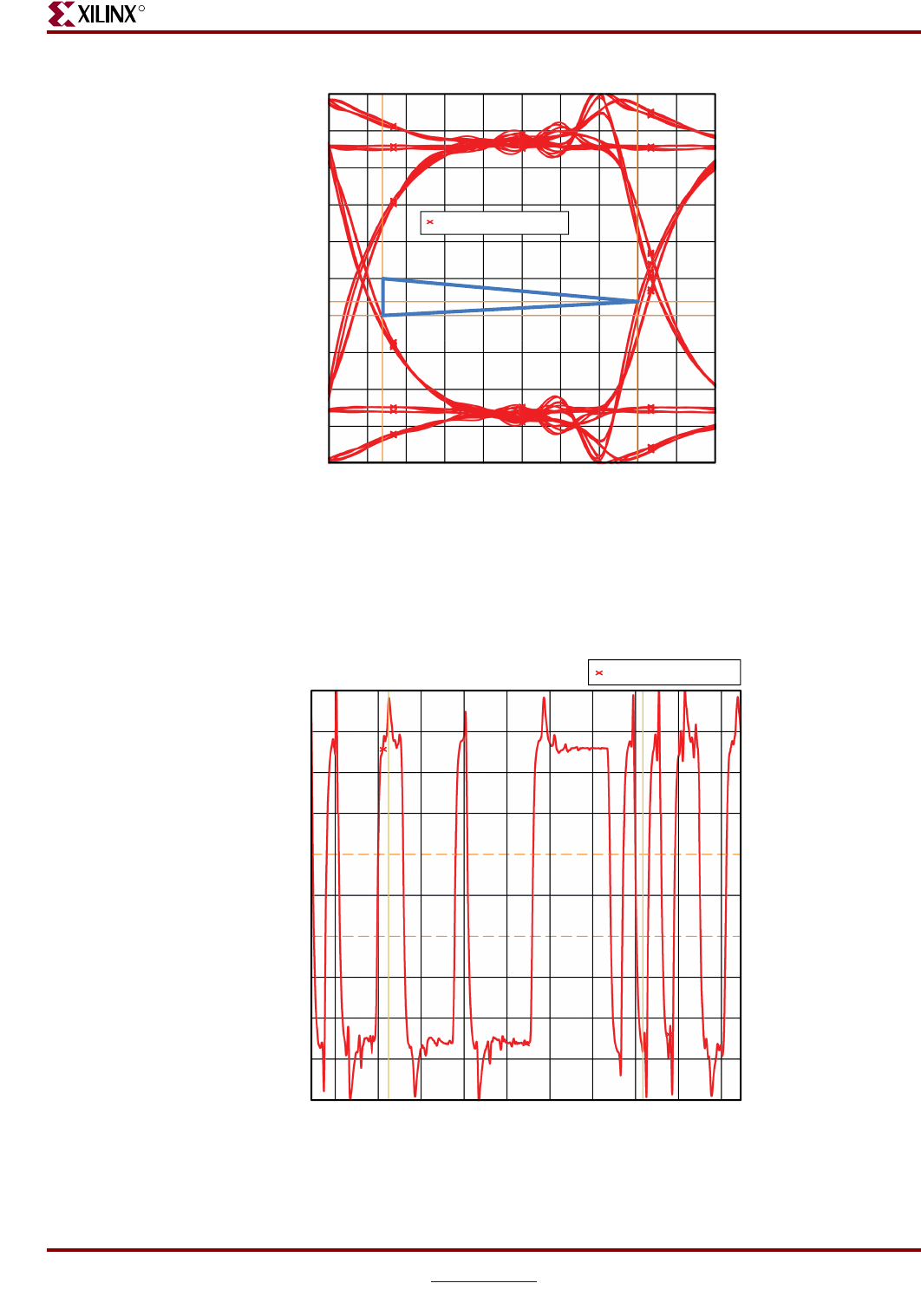
Virtex-5 FPGA ML561 User Guide www.xilinx.com 69
UG199 (v1.2) April 19, 2008
Signal Integrity Correlation Results
R
Figure 7-19: DDR2 Component Read Extrapolation - Eye Scope Shot at Receiver IOB (Fast Corner)
800.0 1200.0 1600.0 2000.0 2400.0 2800.0
-100.0
100.0
300.0
500.0
700.0
900.0
1100.0
1300.0
1500.0
1700.0
1900.0
UG199_c7_19_071007
Time (ps)
Voltage (mV)
Probe 1:U7.P25 (at die)
♦333 MHz, Fast, PRBS6, 88% UI
♦Cursor 1: 701.2 mV, 1.0772 ns
♦Cursor 2: 774.6 mV, 2.3980 ns
♦Delta Voltage = 73.4 mV, Delta Time = 1.3208 ns (88% UI)
Figure 7-20: DDR2 Component Read Extrapolation - Waveform Scope Shot at Receiver IOB (Fast Corner)
65.000 75.000 85.000 95.000 105.000
-100.0
100.0
300.0
500.0
700.0
900.0
1100.0
1300.0
1500.0
1700.0
1900.0
UG199_c7_20_071007
Time (ns)
Voltage (mV)
Probe 1:U7.P25 (at die)
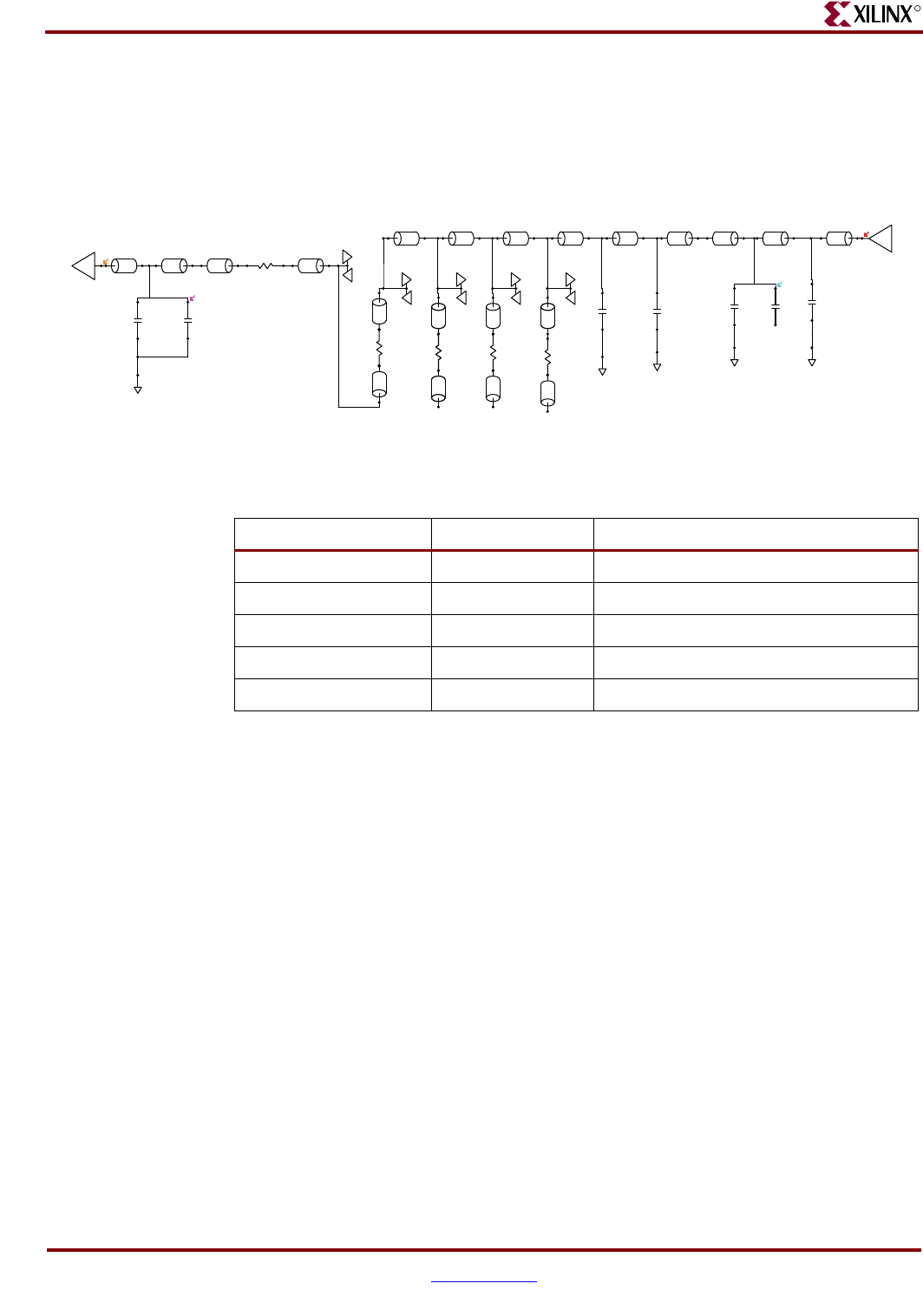
70 www.xilinx.com Virtex-5 FPGA ML561 User Guide
UG199 (v1.2) April 19, 2008
Chapter 7: ML561 Hardware-Simulation Correlation
R
DDR2 DIMM Write Operation
This subsection shows the test results for the DDR2_DIMM_DQ_BY2_B3 signal from
FPGA2 (U5) to the DDR2 DIMM (XP2) measured at 333 MHz (667 Mb/s), where the unit
interval (UI) = 1.5 ns.
The IBIS schematics for DDR2 DIMM interface is extracted from a multi-board project
definition of the two-board combination, which includes the ML561 motherboard and the
DDR2 DIMM at the XP2 connector of the motherboard. The impedance characteristics of
the Molex socket pin (XP2, pin 31) is also included in the IBIS model as a (TL13,
R_00179_CONN_0001, TL14) combination.
The ML561 board under test (S/N 103) is assembled with DDR2 sockets XP3, XP4, and
XP5, which can be utilized for deep DIMM interfaces as described in Table 3-2, page 19 and
Figure 3-2, page 20. To accurately represent the IBIS model of the
DDR2_DIMM_DQ_BY2_B3 signal, the IBIS schematics in Figure 7-21 have added stubs for
the three socket pins at the XP3, XP4, and XP5 connectors.
The DDR2 DIMM used for this correlation testing is a single-rank DIMM part (Micron part
number MT9HTF6472xx-667). Thus for hardware measurements closest to the load, a
probe point via on the DIMM for pin U3.J1 is available.
Figure 7-21: Post-Layout IBIS Schematics of DDR2 DIMM Write Data Bit (DDR2_DIMM_DQ_BY2_B3)
MT47H64M8CB_C...
DQ6
59.8 ohms
3.590 ps
0.022 in
MDQ19_B01
59.8 ohms
31.503 ps
0.195 in
MDQ19_B01
59.8 ohms
78.962 ps
0.490 in
MDQ19_B01
59.8 ohms
10.373 ps
0.064 in
DQ19_B01
49.8 ohms
94.605 ps
0.606 in
DDR2_DIMM_DQ_...
49.8 ohms
90.955 ps
0.582 in
DDR2_DIMM_DQ_...
49.8 ohms
90.340 ps
0.578 in
DDR2_DIMM_DQ_...
49.8 ohms
864.365 ps
5.533 in
DDR2_DIMM_DQ_...
28.5 ohms
4.473 ps
0.028 in
DDR2_DIMM_DQ_...
49.1 ohms
41.316 ps
0.264 in
DDR2_DIMM_DQ_...
49.1 ohms
78.216 ps
0.501 in
DDR2_DIMM_DQ_...
DDR2_DI...
U5_B00.H29
UG199_c7_21_071907
XP5_B00.31XP4_B00.31XP3_B00.31XP2_B00.31
DDR2_DI...
DDR2_DI...DDR2_DI...
59.1 ohms
12.486 ps
AutoPadstk_12_B...
50.3 ohms
23.650 ps
DQ19_B...
50.3 ohms
23.650 ps
DDR2_D...
50.3 ohms
23.650 ps
DDR2_D...
50.3 ohms
23.650 ps
DDR2_D...
50.3 ohms
23.650 ps
DDR2_D...
50.3 ohms
23.650 ps
DQ19_B...
50.3 ohms
23.650 ps
DQ19_B...
50.3 ohms
23.650 ps
DQ19_B...
71.6 ohms
22.319 ps
AutoPadstk_3_B00
TL1 TL5 TL11 TL1222.0 ohms
C13
500.0 fF
17.3 fF
MDQ19_...
0.0 milliohms 0.0 milliohms 0.0 milliohms 0.0 milliohms
RN6_B01
R_00179... R7 R5 R6
TL15 TL16 TL17 TL18
TL24
TL25TL23TL27TL14
????????????
????
TL22TL26
TL13
TL3TL6TL7TL20TL19
U3_B01.J1 J1_B01.31
????
500.0 fF
C8
96.3 fF
46.4 fF253.0 fF
22.9 fF
Virtex-5 FPGA
DDR2_DQ_BY2_B3
Table 7-6: Circuit Elements of DDR2 DIMM Write Data Bit
(DDR2_DIMM_DQ_BY2_B3)
Element Designation Description
Driver U5.H29 FPGA SSTL18_II_DCI_O
Receiver XP2-U3.J1 DDR2 DIMM, 75 Ω ODT
Probe Point C13 Via under memory on DIMM
PCB Termination None ODT at load
Trace Length Multiple TLs 8.975 inches
Virtex-5 FPGA ML561 User Guide www.xilinx.com 71
UG199 (v1.2) April 19, 2008
Signal Integrity Correlation Results
R
DDR2 DQ is a bidirectional signal. To perform hardware measurements for a Write
operation that is not interrupted by a Read response or a Refresh operation, the testbench
on FPGA2 is controlled by DIP switches (SW1) as indicated in Table 7-8.
Table 7-7: DDR2 DIMM Write Operation Correlation Results
Measurement DVW
(%UI)
ISI
(% UI)
Noise Margin
(VIH + VIL) = Total
(% of VREF)
Overshoot / Undershoot
Margin
(% of VREF)
Hardware at Probe
Point
942 ps
(62.8%)
(300 + 200) = 500 ps
(33.3%)
(110 + 100) = 210 mV
(23.3%)
(620 + 620) = 1240 mV
(137.7%)
Simulation correlation
at memory via (C13)
slow-weak corner
1.16 ns
(77.3%)
(80 + 54) = 134 ps
(8.9%)
(172 + 150) = 322 mV
(35.9%)
(606 + 636) =1242 mV
(138%)
Correlation Delta:
HW vs. Simulation
218 ps
(14.5%)
366 ps
(24.4%)
112 mV
(12.6%)
2 mV
(0.3%)
Extrapolation at IOB
slow-weak corner
1.23 ns
(82%)
(85 + 32) = 117 ps
(7.8%)
(178 + 137) = 315 mV
(35.0%)
(604 + 632) = 1236 mV
(137.3%)
Extrapolation at IOB
fast-strong corner
1.32 ns
(88%)
(54 + 46) = 100 ps
(6.7%)
(146 + 107) = 253 mV
(28.1%)
(457 + 524) = 981 mV
(109.0%)
Table 7-8: DIP[1:2] Settings
Setting Description
2’b00 or 2’b11 Normal alternating Write/Read sequence
2’b01 Write only, Refresh disabled
2’b10 Write once, then Read only, Refresh disabled
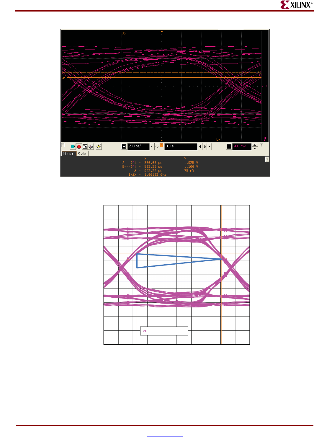
72 www.xilinx.com Virtex-5 FPGA ML561 User Guide
UG199 (v1.2) April 19, 2008
Chapter 7: ML561 Hardware-Simulation Correlation
R
Figure 7-22: DDR2 DIMM Write HW Measurement - Eye Scope Shot at Probe Point #1 (DDR2 Memory Via)
UG199_c7_22_071107
Figure 7-23: DDR2 DIMM Write Correlation - Eye Scope Shot at Probe Point #1 (Slow Corner)
800.0 1200.0 1600.0 2000.0 2400.0 2800.0
-200.0
0.000
200.0
400.0
600.0
800.0
1000.0
1200.0
1400.0
1600.0
1800.0
UG199_c7_23_070907
Time (ps)
Voltage (mV)
Probe 3:C13.1 (at pin)
♦333 MHz, Slow, PRBS6, 77% UI
♦Cursor 1: 1.1004V, 1.2553 ns
♦Cursor 2: 1.0253V, 2.4105 ns
♦Delta Voltage = 75.2 mV, Delta Time = 1.1582 ns (77% UI)
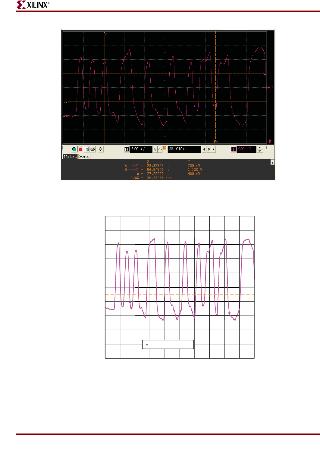
Virtex-5 FPGA ML561 User Guide www.xilinx.com 73
UG199 (v1.2) April 19, 2008
Signal Integrity Correlation Results
R
Figure 7-24: DDR2 DIMM Write HW Measurement - Waveform Scope Shot at Probe Point #1 (DDR2 Memory
Via)
UG199_c7_24_071107
Figure 7-25: DDR2 DIMM Write Correlation - Waveform Scope Shot at Probe Point #1 (Slow Corner)
95.000 105.000 115.000 125.000 135.000 145.000
-200.0
0.000
200.0
400.0
600.0
800.0
1000.0
1200.0
1400.0
1600.0
1800.0
UG199_c7_23_071007
Time (ns)
Voltage (mV)
Probe 3:C13.1 (at pin)
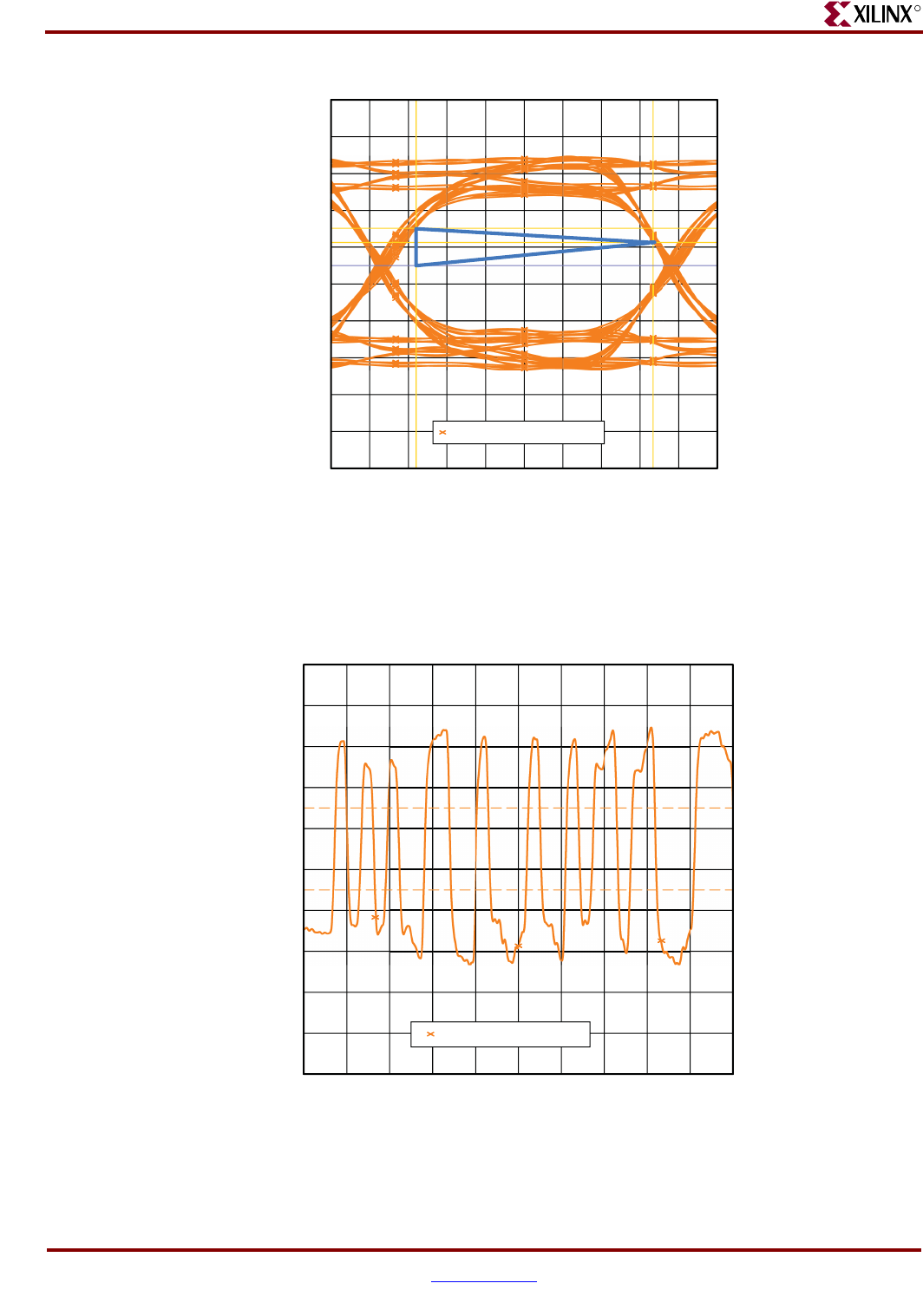
74 www.xilinx.com Virtex-5 FPGA ML561 User Guide
UG199 (v1.2) April 19, 2008
Chapter 7: ML561 Hardware-Simulation Correlation
R
Figure 7-26: DDR2 DIMM Write Extrapolation - Eye Scope Shot at Receiver IOB (Slow Corner)
1000.0 1400.0 1800.0 2200.0 2600.0
-200.0
0.000
200.0
400.0
600.0
800.0
1000.0
1200.0
1400.0
1600.0
1800.0
UG199_c7_26_071007
Time (ps)
Voltage (mV)
Probe 6:U3_B01.J1 (at die)
♦333 MHz, Slow, PRBS6, 82% UI
♦Cursor 1: 1.1028V, 1.2399 ns
♦Cursor 2: 1.0253V, 2.4671 ns
♦Delta Voltage = 77.5 mV, Delta Time = 1.2272 ns (82% UI)
Figure 7-27: DDR2 DIMM Write Extrapolation - Waveform Scope Shot at Receiver IOB (Slow Corner)
95.000 105.000 115.000 125.000 135.000 145.000
-200.0
0.000
200.0
400.0
600.0
800.0
1000.0
1200.0
1400.0
1600.0
1800.0
UG199_c7_27_071007
Time (ns)
Voltage (mV)
Probe 6:U3_B01.J1 (at die)
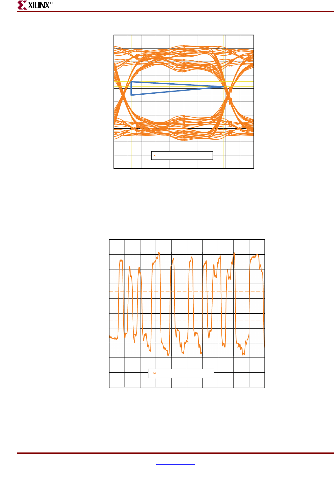
Virtex-5 FPGA ML561 User Guide www.xilinx.com 75
UG199 (v1.2) April 19, 2008
Signal Integrity Correlation Results
R
Figure 7-28: DDR2 DIMM Write Extrapolation - Eye Scope Shot at Receiver IOB (Fast Corner)
400.0 800.0 1200.0 1600.0 2000.0 2400.0
-200.0
0.000
200.0
400.0
600.0
800.0
1000.0
1200.0
1400.0
1600.0
1800.0
UG199_c7_28_071007
Time (ps)
Voltage (mV)
Probe 6:U3_B01.J1 (at die)
♦333 MHz, Fast, PRBS6, 88% UI
♦Cursor 1: 1.1004V, 646.3 ps
♦Cursor 2: 1.0273V, 1.9659 ns
♦Delta Voltage = 73.1 mV, Delta Time = 1.3196 ns (88% UI)
Figure 7-29: DDR2 DIMM Write Extrapolation - Waveform Scope Shot at Receiver IOB (Fast Corner)
95.000 105.000 115.000 125.000 135.000 145.000
0.000
200.0
400.0
600.0
800.0
1000.0
1200.0
1400.0
1600.0
1800.0
UG199_c7_29_071007
Time (ns)
Voltage (mV)
Probe 6:U3_B01.J1 (at die)
76 www.xilinx.com Virtex-5 FPGA ML561 User Guide
UG199 (v1.2) April 19, 2008
Chapter 7: ML561 Hardware-Simulation Correlation
R
DDR2 DIMM Read Operation
This subsection shows the test results for the DDR2_DIMM_DQ_BY2_B3 signal from the
DDR2 DIMM (XP2) to FPGA2 (U5) measured at 333 MHz (667 Mb/s), where the unit
interval (UI) = 1.5 ns.
To perform hardware measurements for a Read operation that is not interrupted by a Write
or a Refresh operation, the testbench on FPGA1 is controlled by the following DIP switch
(SW1) setting:
•DIP[1:2] = 2’b10 – Write once, then Read only, Refresh disabled
Figure 7-30: Post-Layout IBIS Schematics of the DDR2 DIMM Read Data Bit (DDR2_DIMM_DQ_B)
59.8 ohms
78.962 ps
0.490 in
MDQ19_B01
59.8 ohms
31.503 ps
0.195 in
MDQ19_B01
59.8 ohms
3.590 ps
0.022 in
MDQ19_B01
TL11TL1
U3_B01.J1
TL5 22.0 ohms
RN6_B01
MT47H64M8CB_C...
DQ6
C13
500.0 fF
17.3 fF
MDQ19_...
59.8 ohms
10.373 ps
0.064 in
DQ19_B01
TL12
J1_B01.31
????
49.8 ohms
94.605 ps
0.606 in
DDR2_DIMM_DQ_...
49.8 ohms
90.955 ps
0.582 in
DDR2_DIMM_DQ_...
49.8 ohms
90.340 ps
0.578 in
DDR2_DIMM_DQ_...
49.8 ohms
864.365 ps
5.533 in
DDR2_DIMM_DQ_...
59.1 ohms
12.486 ps
AutoPadstk_12_B...
TL15 TL16 TL17 TL18 TL19
XP5_B00.31XP4_B00.31XP3_B00.31XP2_B00.31
TL25TL23TL27TL14
????????????
????
50.3 ohms
23.650 ps
DDR2_D...
50.3 ohms
23.650 ps
DDR2_D...
50.3 ohms
23.650 ps
DDR2_D...
50.3 ohms
23.650 ps
DDR2_D...
0.0 milliohms 0.0 milliohms 0.0 milliohms 0.0 milliohms
R_00179... R7 R5 R6
DDR2_DI...
253.0 fF
50.3 ohms
23.650 ps
DQ19_B...
50.3 ohms
23.650 ps
DQ19_B...
50.3 ohms
23.650 ps
DQ19_B...
50.3 ohms
23.650 ps
DQ19_B...
TL24TL22TL26
TL13
DDR2_DI...
DDR2_DI...
DDR2_DI...
500.0 fF
C8
96.3 fF
46.4 fF
22.9 fF
U5_B00.H29
Virtex-5 FPGA
DIMM_DQ_BY2_B3
28.5 ohms
4.473 ps
0.028 in
DDR2_DIMM_DQ_...
49.1 ohms
41.316 ps
0.264 in
DDR2_DIMM_DQ_...
49.1 ohms
78.216 ps
0.501 in
DDR2_DIMM_DQ_...
71.6 ohms
22.319 ps
AutoPadstk_3_B00
TL3TL6TL7TL20
UG199_c7_30_071907
Table 7-9: Circuit Elements of DDR2 DIMM Read Data Bit
(DDR2_DIMM_DQ_BY2_B3)
Element Designation Description
Driver XP2-U3.J1 DDR2 DIMM
Receiver U5.H29 FPGA SSTL18_II_DCI_I
Probe Point C8 Via under FPGA2 (U5.H29)
PCB Termination None DCI at load
Trace Length Multiple TLs 8.975 inches
Table 7-10: DDR2 DIMM Read Operation Correlation Results
Measurement DVW (%
UI)
ISI
(% UI)
Noise Margin
(VIH + VIL) = Total
(% of VREF)
Overshoot / Undershoot
Margin
(% of VREF)
Hardware at probe
point
904 ps
(60%)
(107 + 62) = 169 ps
(11.2%) (242 + 258) = 500 mV (623 + 613) = 1236 mV
(137.3%)
Simulation correlation
slow-weak corner
865 ps
(59%)
(130 + 83) = 213 ps
(14.2%) (+292 + 298) = 590 mV (524 + 504) = 1028 mV
(114.2%)
Correlation Delta:
HW vs. Simulation
39 ps
(2.6%) 44 ps (2.9%) 90 mV (10%) 208 mV (23.1%)
Extrapolation at IOB
slow-weak corner
1.23 ns
(82%)
(139 + 75) = 224 ps
(14.9%)
(243 + 303) = 546 mV
(60.7%)
(594 + 544) = 1138 mV
(116.5%)
Extrapolation at IOB
fast-strong corner
1.24 ns
(83%)
(131 + 60) = 191 ps
(12.7%)
(288 + 282) = 570 mV
(63.3%)
(+481 + 508) = 989 mV
(109.9%)
Virtex-5 FPGA ML561 User Guide www.xilinx.com 77
UG199 (v1.2) April 19, 2008
Signal Integrity Correlation Results
R
Figure 7-31: DDR2 DIMM Read HW Measurement - Eye Scope Shot at Probe Point (FPGA1 Via)
UG199_c7_31_071107
Figure 7-32: DDR2 DIMM Read Correlation - Eye Scope Shot at Probe Point (Slow Corner)
2000.0 2400.0 2800.0 3200.0 3600.0
-100.0
100.0
300.0
500.0
700.0
900.0
1100.0
1300.0
1500.0
1700.0
1900.0
Time (ps)
Voltage (mV)
UG199_c7_32_071107
Probe 3:C8.1 (at pin)
♦333 MHz, Slow, PRBS6, 59% UI
♦Cursor 1: 1.0988V, 2.5207 ns
♦Cursor 2: 1.0254V, 3.3859 ns
♦Delta Voltage = 73.4 mV, Delta Time = 865.2 ps (59% UI)

78 www.xilinx.com Virtex-5 FPGA ML561 User Guide
UG199 (v1.2) April 19, 2008
Chapter 7: ML561 Hardware-Simulation Correlation
R
Figure 7-33: DDR2 DIMM Read HW Measurement - Waveform Scope Shot at Probe Point (FPGA1 Via)
UG199_c7_33_071107
Figure 7-34: DDR2 DIMM Read Correlation - Waveform Scope Shot at Probe Point (Slow Corner)
25.000 35.000 45.000 55.000 65.000 75.000
-200.0
0.000
200.0
400.0
600.0
800.0
1000.0
1200.0
1400.0
1600.0
1800.0
Time (ns)
Voltage (mV)
UG199_c7_34_071007
Probe 3:C8.1 (at pin)
Virtex-5 FPGA ML561 User Guide www.xilinx.com 79
UG199 (v1.2) April 19, 2008
Signal Integrity Correlation Results
R
Figure 7-35: DDR2 DIMM Read Extrapolation - Eye Scope Shot at Receiver IOB (Slow Corner)
2000.0 2400.0 2800.0 3200.0 3600.0 4000.0
-200.0
0.000
200.0
400.0
600.0
800.0
1000.0
1200.0
1400.0
1600.0
1800.0
Time (ps)
Voltage (mV)
UG199_c7_35_071007
Probe 6:U5_B00.H29 (at die)
♦333 MHz, Slow, PRBS6, 82% UI
♦Cursor 1: 1.1007V, 2.3997 ns
♦Cursor 2: 1.0232V, 3.6257 ns
♦Delta Voltage = 77.5 mV, Delta Time = 1.2260 ns (82% UI)
Figure 7-36: DDR2 DIMM Read Extrapolation - Waveform Scope Shot at Receiver IOB (Slow Corner)
30.000 40.000 50.000 60.000 70.000
-200.0
0.000
200.0
400.0
600.0
800.0
1000.0
1200.0
1400.0
1600.0
1800.0
UG199_c7_36_071007
Time (ns)
Voltage (mV)
Probe 6:U5_B00.H29 (at die)
80 www.xilinx.com Virtex-5 FPGA ML561 User Guide
UG199 (v1.2) April 19, 2008
Chapter 7: ML561 Hardware-Simulation Correlation
R
Figure 7-37: DDR2 DIMM Read Extrapolation - Eye Scope Shot at Receiver IOB (Fast Corner)
400.0 800.0 1200.0 1600.0 2000.0 2400.0
-200.0
0.000
200.0
400.0
600.0
800.0
1000.0
1200.0
1400.0
1600.0
1800.0
Time (ps)
Voltage (mV)
UG199_c7_37_071007
Probe 6:U5_B00.H29 (at die)
♦333 MHz, Fast, PRBS6, 83% UI
♦Cursor 1: 697.0 mV, 763.0 ps
♦Cursor 2: 776.6 mV, 2.0052 ns
♦Delta Voltage = 79.5 mV, Delta Time = 1.2422 ns (83% UI)
Figure 7-38: DDR2 DIMM Read Extrapolation - Waveform Scope Shot at Receiver IOB (Fast Corner)
30.000 40.000 50.000 60.000 70.000
-200.0
0.000
200.0
400.0
600.0
800.0
1000.0
1200.0
1400.0
1600.0
1800.0
UG199_c7_38_071007
Time (ns)
Voltage (mV)
Probe 6:U5_B00.H29 (at die)
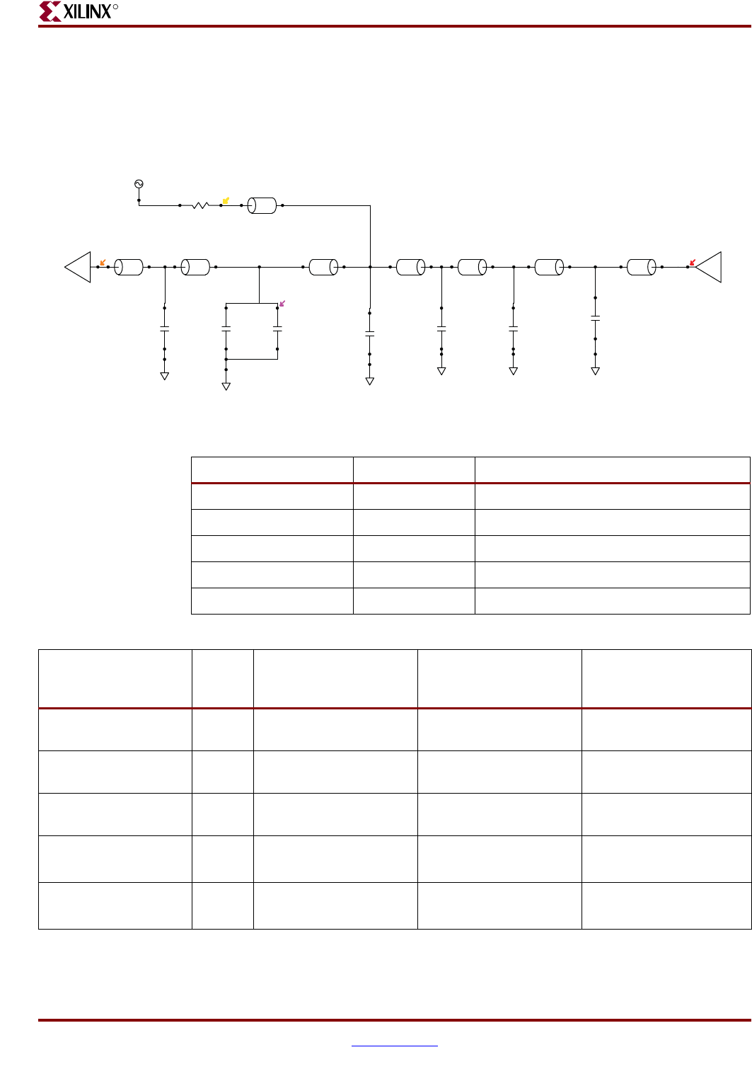
Virtex-5 FPGA ML561 User Guide www.xilinx.com 81
UG199 (v1.2) April 19, 2008
Signal Integrity Correlation Results
R
QDRII Write Operation
This subsection shows the test results for the QDR2_D_BY0_B5 signal from FPGA3 (U34)
to QDRII memory (U35) measured at 300 MHz (600 Mb/s), where the unit interval
(UI) = 167 ns.
Figure 7-39: Post-Layout IBIS Schematics of QDRII Write Data Bit (QDR2_D_BY0_B5)
K7R323684M_1.8V
D5
C7
500.0 fF 58.1 fF 399.1 fF 177.3 fF 22.9 fF
22.9 fF22.9 fF
U35.G11
28.5 ohms
4.404 ps
0.027 in
QDR2_D_BY0_B5
49.0 ohms
11.902 ps
0.079 in
QDR2_D_BY0_B5
49.8 ohms
520.665 ps
3.333 in
QDR2_D_BY0_B5
28.5 ohms
4.473 ps
0.028 in
QDR2_D_BY0_B5
Virtex-5 FPGA
QDR2_D_BY0_B5
U34.M31
UG199_c7_39_070907
49.0 ohms
5.283 ps
0.035 in
QDR2_D_BY0_B5
71.0 ohms
27.482 ps
AutoPadstk_3
45.1 ohms
7.862 ps
AutoPadstk_19
70.8 ohms
16.339 ps
AutoPadstk_3
TL2 TL4 TL5
TL6
TL7 TL8 TL3 TL1
QDR2_D... QDR2_D... QDR2_D... QDR2_D...
QDR2_D...
QDR2_D...
R1586
VCC0V7…
0.9V
49.9 ohms
Table 7-11: Circuit Elements of QDRII Write Data bit (QDR2_D_BY0_B5)
Element Designation Description
Driver U34.M31 FPGA HSTL_I_18
Receiver U35.G11 QDRII memory
Probe Point C7 Via under Memory
PCB Termination R1586 External termination at memory
Trace Length TL 2, 5, 8, 1 3.46 inches
Table 7-12: QDRII Write Operation Correlation Results
Measurement DVW
(% UI)
ISI
(% UI)
Noise Margin
(VIH + VIL) = Total
(% of VREF)
Overshoot / Undershoot
Margin
(% of VREF)
Hardware at probe
point
1.40 ns
(84.1%) (50 + 70) = 120 ps (7.2%) (340 + 400) = 740 mV
(82.2%)
(450 + 400) = 850 mV
(94.5%)
Simulation correlation
slow-weak corner
1.39 ns
(83.5%) (136 + 91) = 227 ps (13.6%) (344 + 398) = 742 mV
(82.5%)
(483 + 452) = 935 mV
(103.9%)
Correlation Delta:
HW vs. Simulation
10 ps
(0.6%) 107 ps (6.4%) 2 mV (0.3%) 85 mV (9.4%)
Extrapolation at IOB
slow-weak corner
1.38 ns
(83%)
(172 + 141) = 313 ps
(18.8%)
(329 + 358) = 687 mV
(76.3%)
(400 + 361) = 761 mV
(84.5%)
Extrapolation at IOB
fast-strong corner
1.49 ns
(89%) (126 + 91) = 217 ps (13.0%) (353 + 376) = 729 mV
(81.0%)
(156 + 30) = 186 mV
(20.7%)
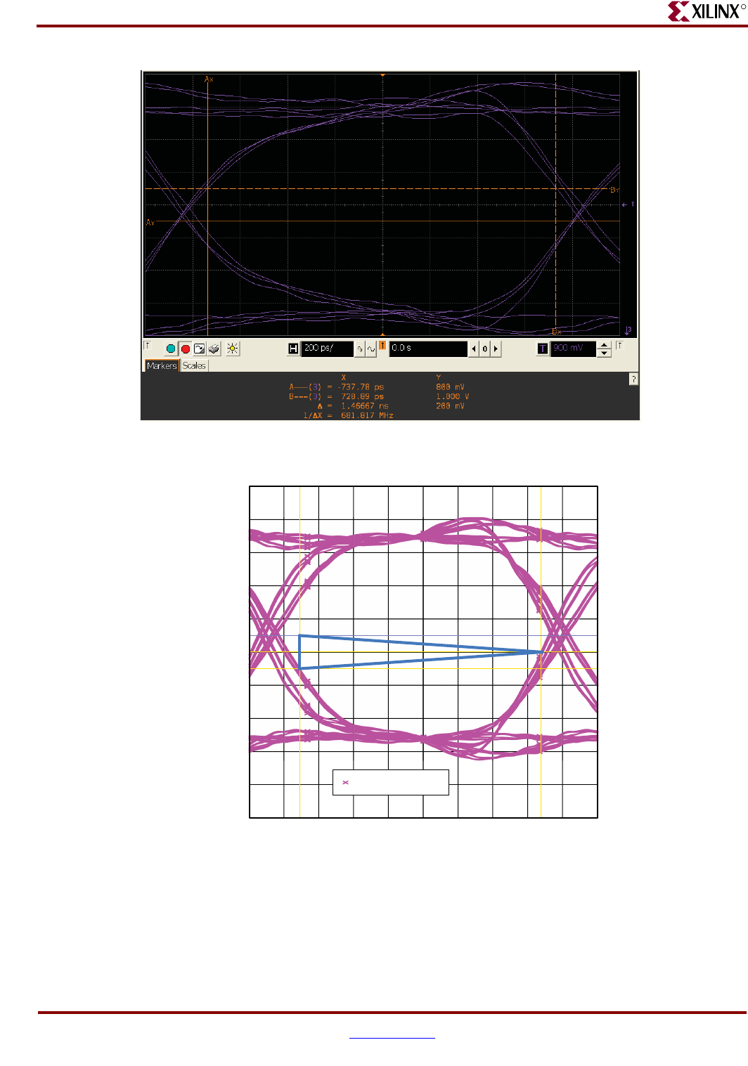
82 www.xilinx.com Virtex-5 FPGA ML561 User Guide
UG199 (v1.2) April 19, 2008
Chapter 7: ML561 Hardware-Simulation Correlation
R
Figure 7-40: QDRII Write HW Measurement - Eye Scope Shot at Probe Point (QDRII Memory Via)
UG199_c7_40_071107
Figure 7-41: QDRII Write Correlation - Eye Scope Shot at Probe Point (Slow Corner)
0.000 400.0 800.0 1200.0 1600.0
-200.0
0.000
200.0
400.0
600.0
800.0
1000.0
1200.0
1400.0
1600.0
1800.0
Time (ps)
Voltage (mV)
UG199_c7_41_070907
Probe 3:C7.1 (at pin)
♦300 MHz, Slow, PRBS6, 83.5% UI
♦Cursor 1: 699.1 mV, 90.0 ps
♦Cursor 2: 801.0 mV, 1.4770 ns
♦Delta Voltage = 101.9 mV, Delta Time = 1.3870 ns (83.5% UI)
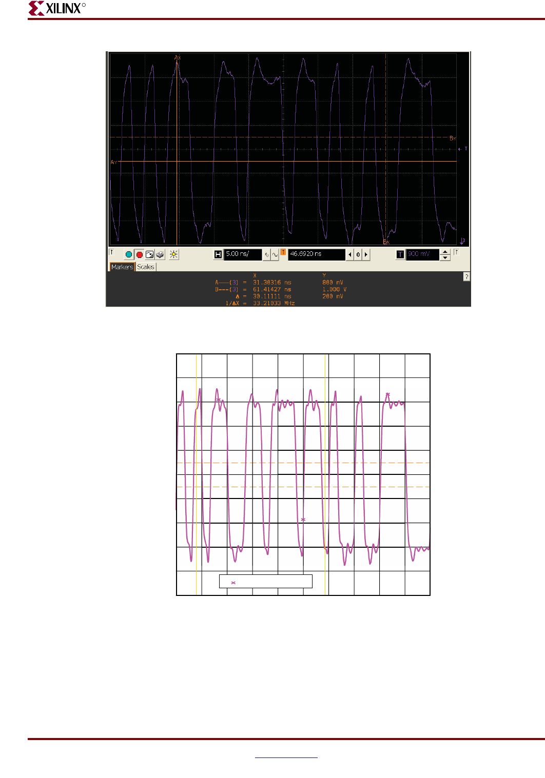
Virtex-5 FPGA ML561 User Guide www.xilinx.com 83
UG199 (v1.2) April 19, 2008
Signal Integrity Correlation Results
R
Figure 7-42: QDRII Write HW Measurement - Waveform Scope Shot at Probe Point (QDRII Memory Via)
UG199_c7_42_071107
Figure 7-43: QDRII Write Correlation - Waveform Scope Shot at Probe Point (Slow Corner)
110.000 120.000 130.000 140.000 150.000 160.000
-100.0
100.0
300.0
500.0
700.0
900.0
1100.0
1300.0
1500.0
1700.0
1900.0
Time (ns)
Voltage (mV)
UG199_c7_43_071007
Probe 3:C7.1 (at pin)
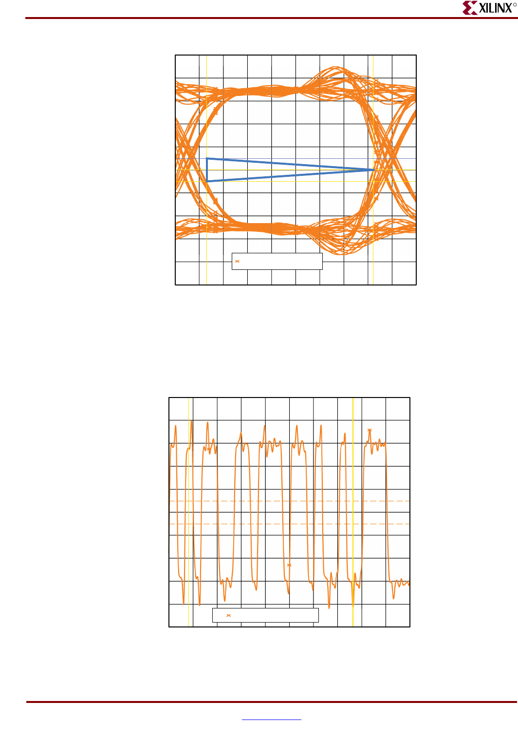
84 www.xilinx.com Virtex-5 FPGA ML561 User Guide
UG199 (v1.2) April 19, 2008
Chapter 7: ML561 Hardware-Simulation Correlation
R
Figure 7-44: QDRII Write Extrapolation - Eye Scope Shot at Receiver IOB (Slow Corner)
0.000 400.0 800.0 1200.0 1600.0
-200.0
0.000
200.0
400.0
600.0
800.0
1000.0
1200.0
1400.0
1600.0
1800.0
Time (ps)
Voltage (mV)
UG199_c7_44_070907
Probe 6:U35.G11 (at die)
♦300 MHz, Slow, PRBS6, 83% UI
♦Cursor 1: 699.1 mV, 61.3 ps
♦Cursor 2: 801.0 mV, 1.4433 ns
♦Delta Voltage = 101.9 mV, Delta Time = 1.3820 ns (83% UI)
Figure 7-45: QDRII Write Extrapolation - Waveform Scope Shot at Receiver IOB (Slow Corner)
110.000 120.000 130.000 140.000 150.000 160.000
-100.0
100.0
300.0
500.0
700.0
900.0
1100.0
1300.0
1500.0
1700.0
1900.0
UG199_c7_45_071007
Time (ns)
Voltage (mV)
Probe 6:U35.G11 (at die)
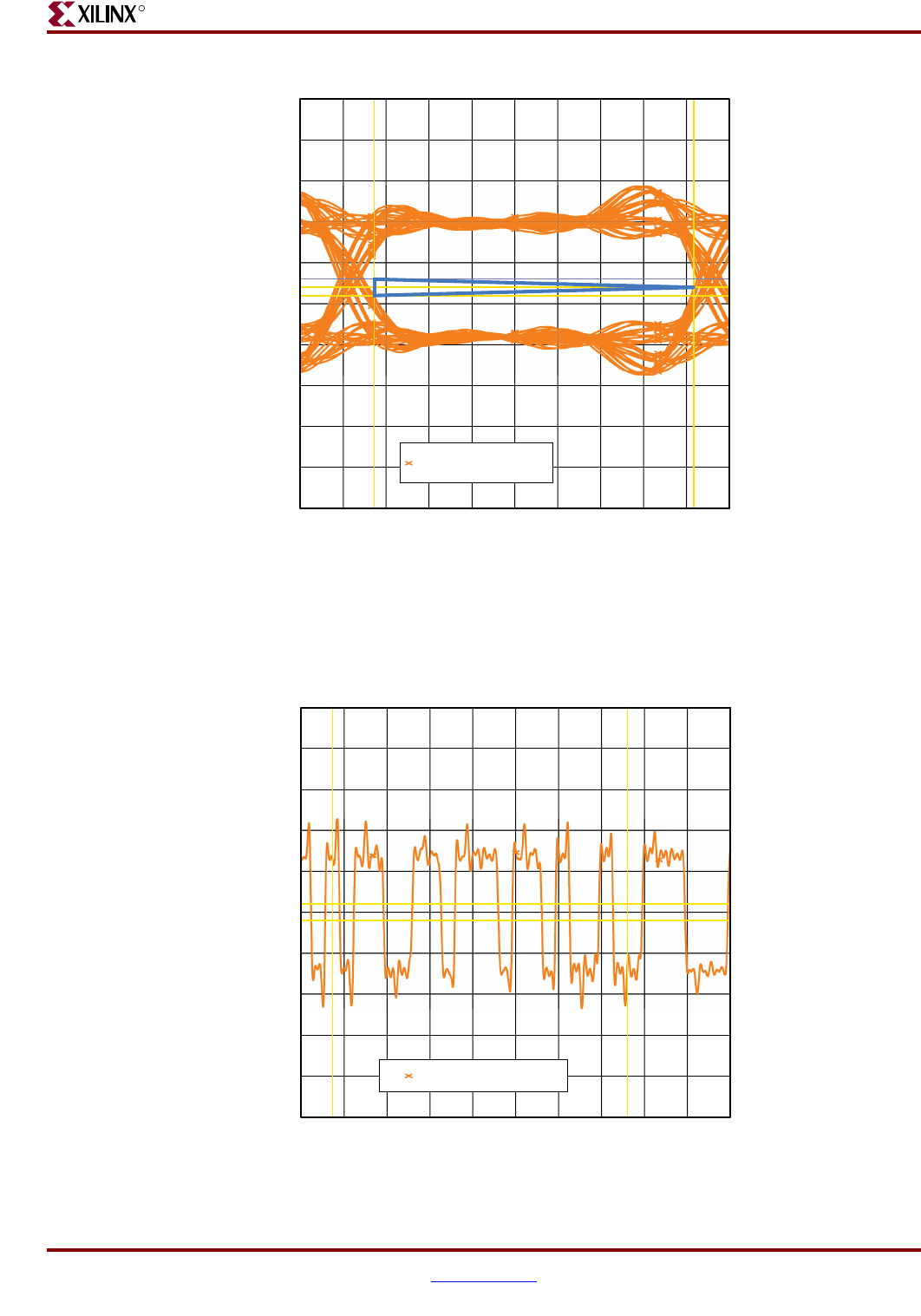
Virtex-5 FPGA ML561 User Guide www.xilinx.com 85
UG199 (v1.2) April 19, 2008
Signal Integrity Correlation Results
R
Figure 7-46: QDRII Write Extrapolation - Eye Scope Shot at Receiver IOB (Fast Corner)
800.0 1200.0 1600.0 2000.0 2400.0 2800.0
-1900.0
-1400.0
-900.0
-400.0
100.0
600.0
1100.0
1600.0
2100.0
2600.0
3100.0
Time (ps)
Voltage (mV)
UG199_c7_46_070907
Probe 6:U35.G11 (at die)
♦300 MHz, Fast, PRBS6, 89% UI
♦Cursor 1: 699.1 mV, 1.1440 ns
♦Cursor 2: 801.0 mV, 2.6334 ns
♦Delta Voltage = 101.9 mV, Delta Time = 1.4894 ns (89% UI)
Figure 7-47: QDRII Write Extrapolation - Waveform Scope Shot at Receiver IOB (Fast Corner)
110.000 120.000 130.000 140.000 150.000 160.000
-1600.0
-1100.0
-600.0
-100.0
400.0
900.0
1400.0
1900.0
2400.0
2900.0
3400.0
UG199_c7_47_070907
Time (ns)
Voltage (mV)
Probe 6:U35.G11 (at die)
86 www.xilinx.com Virtex-5 FPGA ML561 User Guide
UG199 (v1.2) April 19, 2008
Chapter 7: ML561 Hardware-Simulation Correlation
R
QDRII Read Operation
This subsection shows the test results for the QDR2_Q_BY0_B5 signal from QDRII
memory (U35) to FPGA3 (U34) measured at 300 MHz (600 Mb/s), where the unit interval
(UI) = 1.67 ns.
Figure 7-48: Post-Layout IBIS Schematics of QDRII Read Data Bit (QDR2_Q_BY0_B5)
Virtex-5 FPGA
QDR2_Q_BY0_B5
U34.G33
28.5 ohms
4.473 ps
0.028 in
QDR2_Q_BY0_B5
49.1 ohms
95.834 ps
0.613 in
QDR2_Q_BY0_B5
28.5 ohms
4.404 ps
0.027 in
QDR2_Q_BY0_B5
49.1 ohms
427.654 ps
2.737 in
QDR2_Q_BY0_B5
71.6 ohms
22.319 ps
AutoPadstk_3
71.8 ohms
22.319 ps
AutoPad...
TL1 TL2 TL3 TL6 TL7 TL8
22.9 fF 96.3 fF 500.0 fF
513.2 fF
C7
QDR2_Q...
QDR2_Q...
QDR2_Q...
96.3 fF
QDR2_Q...
22.9 fF
QDR2_Q...
U35.F11
UG199_c7_48_071907
K7R323684M_1.8V
C5
Table 7-13: Circuit Elements of QDRII Read Data Bit (QDR2_Q_BY0_B5)
Element Designation Description
Driver U36.F11 QDRII memory
Receiver U34.G33 FPGA HSTL_I_DCI_18
Probe Point C7 Via under FPGA3 (U34)
PCB Termination None DCI at FPGA
Trace Length TL 1, 3, 6, 8 3.41 inches
Table 7-14: QDRII Read Operation Correlation Results
Measurement DVW
(% UI)
ISI
(% UI)
Noise Margin
(VIH + VIL) = Total
(% of VREF)
Overshoot / Undershoot
Margin
(% of VREF)
Hardware at probe point 1.09 ns
(65.4%) (70 + 50) = 120 ps (7.2%) (400 + 400) = 800 mV
(88.9%)
(500 + 500) = 1000 mV
(111.1%)
Simulation correlation
slow-weak corner
984 ps
(59.0%) (72 + 75) = 147 ps (8.8%) (250 + 264) = 514 mV
(57.1%)
(532 + 518) = 1050 mV
(105.5%)
Correlation Delta:
HW vs. Simulation
106 ps
(6.4%) 27 ps (1.6%) 386 mV (31.8%) 50 mV (5.6%)
Extrapolation at IOB
slow-weak corner
1.46 ns
(88%) (49 + 36) = 85 ps (5.1%) (237 + 272) = 509 mV
(56.5%)
(608 + 575) = 1183 mV
(131.5%)
Extrapolation at IOB
fast-strong corner
1.45 ns
(87%) (27 + 39) = 66 ps (4.0%) (341 +201) = 542 mV
(60.3%)
(532 + 661) = 1193 mV
(132.6%)
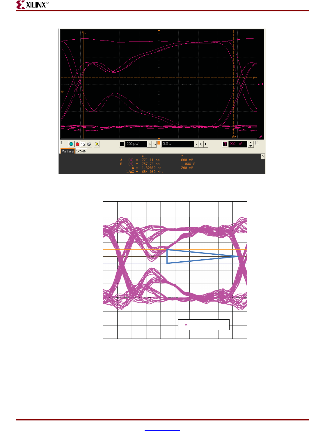
Virtex-5 FPGA ML561 User Guide www.xilinx.com 87
UG199 (v1.2) April 19, 2008
Signal Integrity Correlation Results
R
Figure 7-49: QDRII Read HW Measurement - Eye Diagram Scope Shot at Probe Point (FPGA3 Via)
UG199_c7_49_071107
Figure 7-50: QDRII Read Correlation - Eye Diagram Scope Shot at Probe Point (Slow Corner)
800.0 1200.0 1600.0 2000.0 2400.0
-200.0
0.000
200.0
400.0
600.0
800.0
1000.0
1200.0
1400.0
1600.0
1800.0
Time (ps)
Voltage (mV)
UG199_c7_50_070907
Probe 3:C7.1 (at pin)
♦300 MHz, Slow, PRBS6, 59% UI
♦Cursor 1: 1.1007V, 1.4881 ns
♦Cursor 2: 1.0029V, 2.4719 ns
♦Delta Voltage = 97.9 mV, Delta Time = 983.8 ps (59% UI)
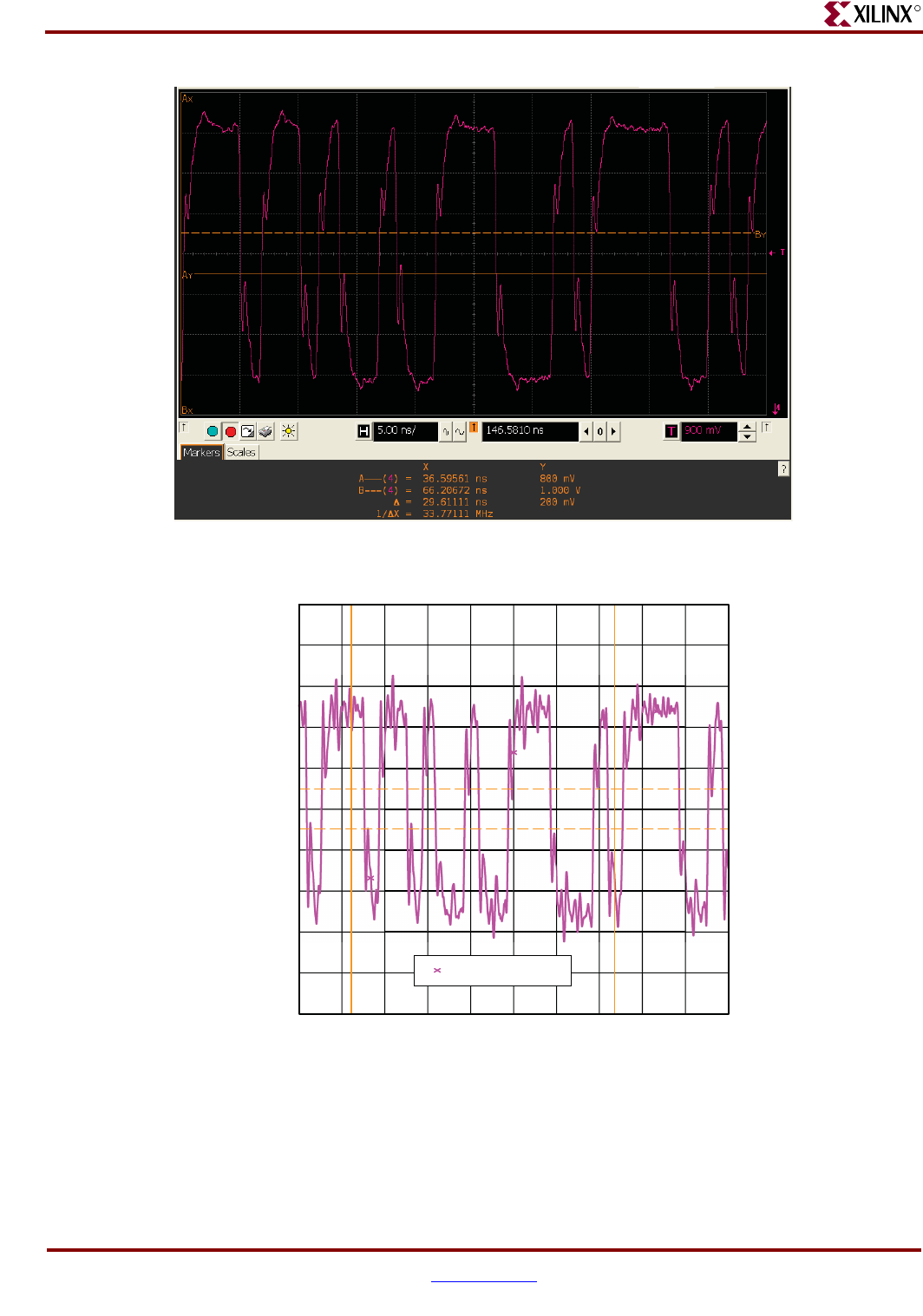
88 www.xilinx.com Virtex-5 FPGA ML561 User Guide
UG199 (v1.2) April 19, 2008
Chapter 7: ML561 Hardware-Simulation Correlation
R
Figure 7-51: QDRII Read HW Measurement - Waveform Scope Shot at Probe Point (FPGA3 Via)
UG199_c7_51_071107
Figure 7-52: QDRII Read Correlation - Waveform Scope Shot at Probe Point (Slow Corner)
20.000 30.000 40.000 50.000 60.000 70.000
-100.0
100.0
300.0
500.0
700.0
900.0
1100.0
1300.0
1500.0
1700.0
1900.0
Time (ns)
Voltage (mV)
UG199_c7_52_071007
Probe 3:C7.1 (at pin)
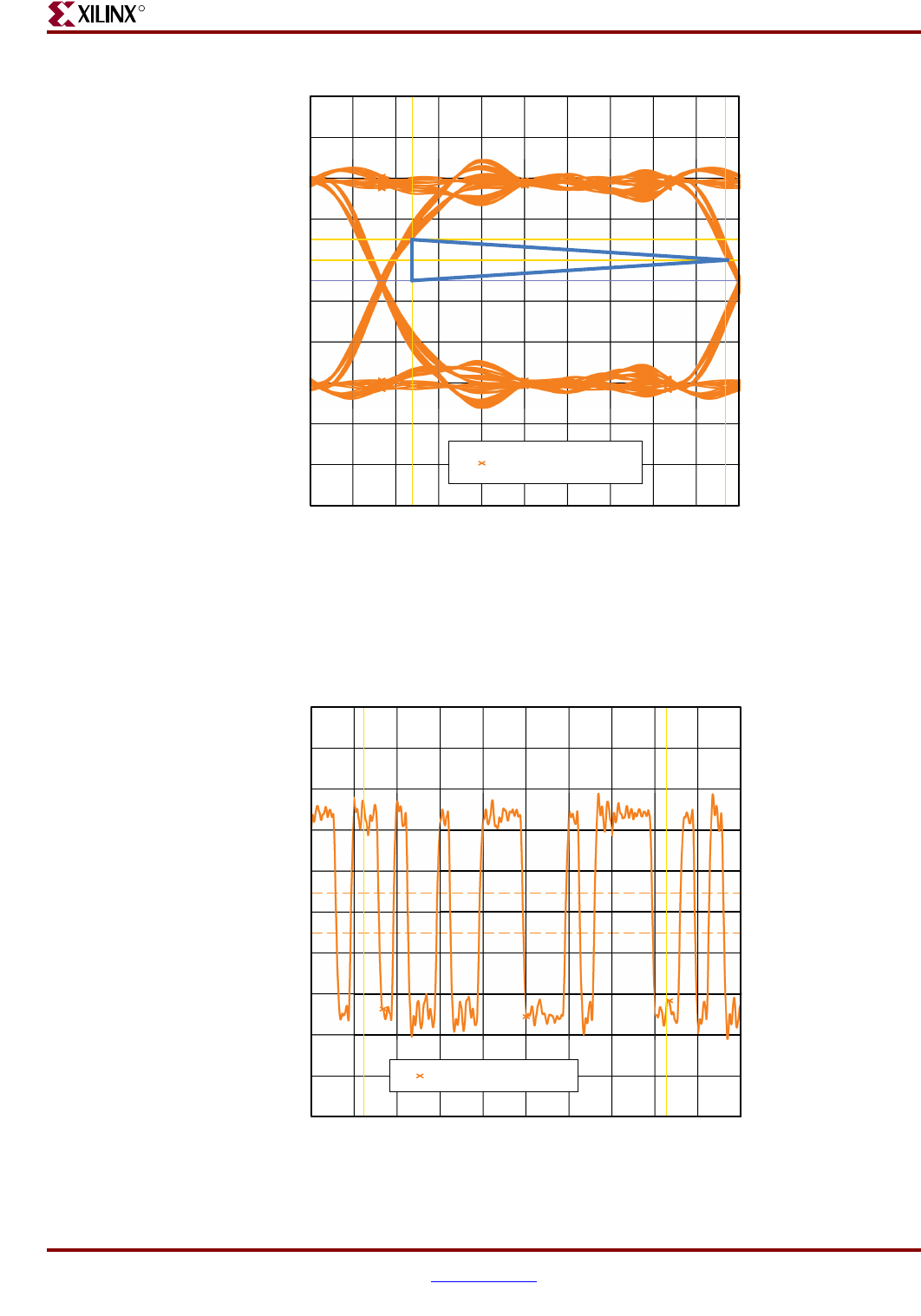
Virtex-5 FPGA ML561 User Guide www.xilinx.com 89
UG199 (v1.2) April 19, 2008
Signal Integrity Correlation Results
R
Figure 7-53: QDRII Read Extrapolation - Eye Scope Shot at Receiver IOB (Slow Corner)
1000.0 1400.0 1800.0 2200.0 2600.0
-200.0
0.000
200.0
400.0
600.0
800.0
1000.0
1200.0
1400.0
1600.0
1800.0
Time (ps)
Voltage (mV)
UG199_c7_53_070907
Probe 6:U34.G33 (at die)
♦300 MHz, Slow, PRBS6, 88% UI
♦Cursor 1: 1.1008V, 1.2758 ns
♦Cursor 2: 998.9 mV, 2.7352 ns
♦Delta Voltage = 101.9 mV, Delta Time = 1.4594 ns (88% UI)
Figure 7-54: QDRII Read Extrapolation - Waveform Scope Shot at Receiver IOB (Slow Corner
30.000 40.000 50.000 60.000 70.000
-100.0
100.0
300.0
500.0
700.0
900.0
1100.0
1300.0
1500.0
1700.0
1900.0
UG199_c7_54_071007
Time (ns)
Voltage (mV)
Probe 6:U34.G33 (at die)
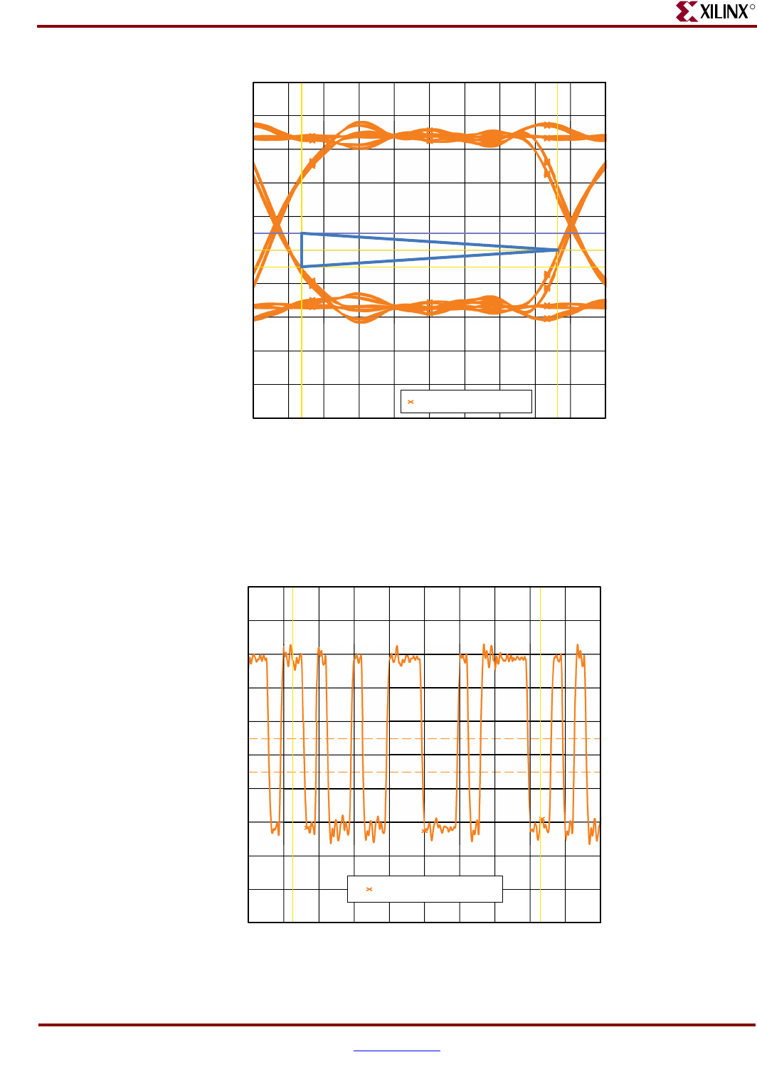
90 www.xilinx.com Virtex-5 FPGA ML561 User Guide
UG199 (v1.2) April 19, 2008
Chapter 7: ML561 Hardware-Simulation Correlation
R
Figure 7-55: QDRII Read Extrapolation - Eye Scope Shot at Receiver IOB (Fast Corner)
1200.0 1600.0 2000.0 2400.0 2800.0
-200.0
0.000
200.0
400.0
600.0
800.0
1000.0
1200.0
1400.0
1600.0
1800.0
Time (ps)
Voltage (mV)
UG199_c7_55_070907
Probe 6:U34.G33 (at die)
♦300 MHz, Fast, PRBS6, 87% UI
♦Cursor 1: 801 mV, 2.7263 ns
♦Cursor 2: 697.0 mV, 1.2744 ns
♦Delta Voltage = 104.0 mV, Delta Time = 1.4519 ns (87% UI)
Figure 7-56: QDRII Read Extrapolation - Waveform Scope Shot at Receiver IOB (Fast Corner)
25.000 35.000 45.000 55.000 65.000 75.000
-100.0
100.0
300.0
500.0
700.0
900.0
1100.0
1300.0
1500.0
1700.0
1900.0
UG199_c7_56_071007
Time (ns)
Voltage (mV)
Probe 6:U34.G33 (at die)
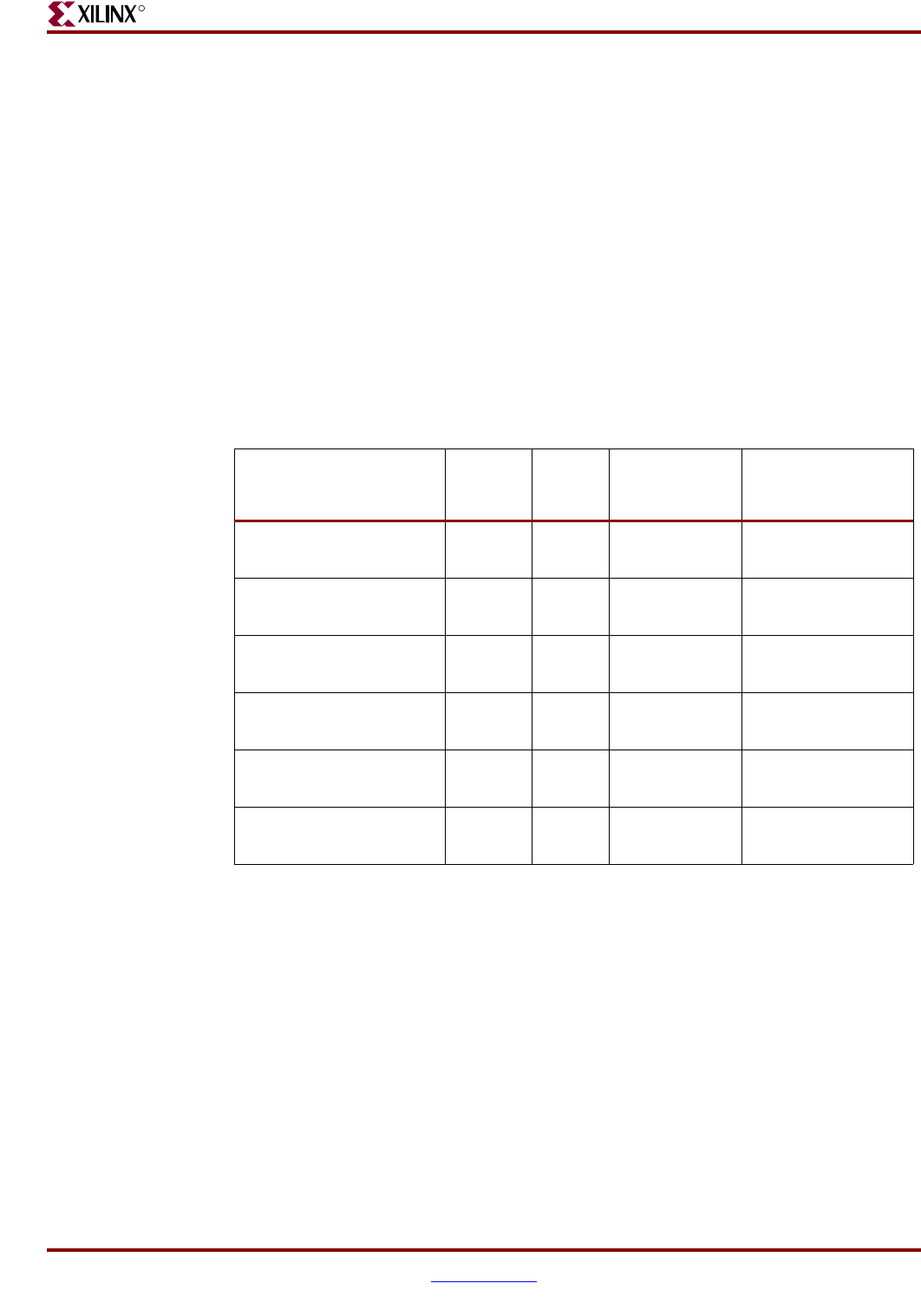
Virtex-5 FPGA ML561 User Guide www.xilinx.com 91
UG199 (v1.2) April 19, 2008
Summary and Recommendations
R
Summary and Recommendations
The first objective of this exercise is to establish correlation between hardware
measurements and the simulation at the probe point. The intention was to validate the
simulation model for the targeted signal. The degree of correlation achieved is looked at in
terms of absolute difference as well as relative percentage. The relative percentage
differences are presented in terms of unit interval (UI) for timing characteristics and in
terms of VREF voltage for the voltage margin characteristics.
Correlation simulation is performed under ideal conditions, that is, the stimulus is
generated without any jitter. On the other hand, the hardware measurements are subject to
jitter (which tends to increase ISI), board-level power fluctuation (which can affect the eye
amplitude), and stability of the probing station. Thus some correlation differences are
expected. The user ultimately uses his or her own judgment to account for these
differences, and adjusts the values extrapolated for quality of signal at the receiver IOB.
Table 7-15 contains this information for all six test signals.
There are varying degrees of correlation differences among the six test signals. In general,
there is a good match between hardware measurements and the correlation simulation,
except for some yet-to-be analyzed differences, for example, DDR2 DIMM Write DVW and
QDRII read noise margin.
The remainder of this section summarizes the extrapolation results of the data bit interface
for all six memory operations on the ML561 board. The measure of SI characteristics of
each signal is determined by the worst-case extrapolation measurement from among the
simulations with drivers at slow-weak and fast-strong corners. The values chosen between
these two corner cases are:
•Minimum of DVW, noise margin, and overshoot/undershoot margin
•Maximum of ISI
Table 7-15: Summary of Correlation Differences: Hardware vs. Simulation
Operation ΔDVW
(% UI(1))
ΔISI
(% UI)
Noise Margin
(% VREF)
Overshoot /
Undershoot Margin
(% VREF)
DDR2 Component Write 40 ps
(2.6%)
47 ps
(3.2%)
98 mV
(10.9%)
69 mV
(7.6%)
DDR2 Component Read 0 ps
(0%)
43 ps
(2.9%)
6 mV
(0.7%)
244 mV
(17.2%)
DDR2 DIMM Write 218 ps
(14.5%)
366 ps
(24.5%)
112 mV
(12.6%)
2 mV
(0.3%)
DDR2 DIMM Read 39 ps
(2.6%)
44 ps
(2.9%)
90 mV
(10.0%)
208 mV
(23.1%)
QDRII Write 10 ps
(0.6%)
107 ps
(6.4%)
2 mV
(0.3%)
85 mV
(9.4%)
QDRII Read 106 ps
(6.4%)
27 ps
(1.6%)
386 mV
(31.8%)
50 mV
(5.6%)
Notes:
1. Unit Interval (UI): 1.5 ns for DDR2 and 1.67 ns for QDRII. VREF = 0.9V for DDR2 and QDRII.
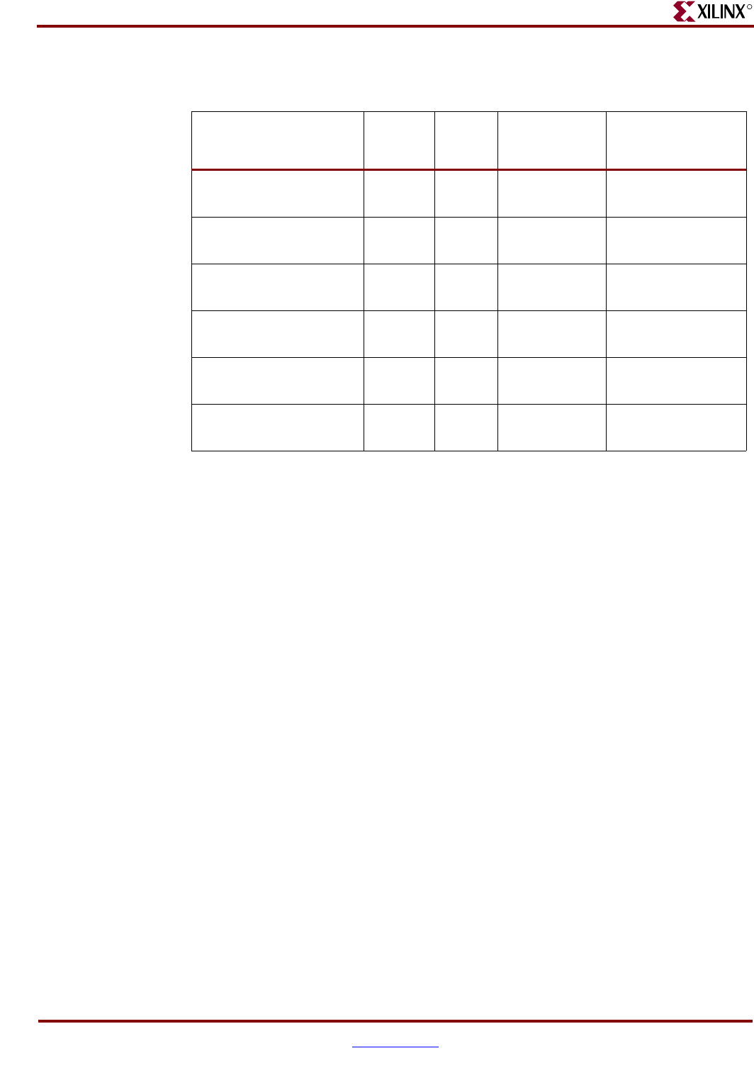
92 www.xilinx.com Virtex-5 FPGA ML561 User Guide
UG199 (v1.2) April 19, 2008
Chapter 7: ML561 Hardware-Simulation Correlation
R
Table 7-16 summarizes the extrapolated SI characteristics of all six test signals.
Here are some observations about extrapolated SI characteristics among these test signals:
•The Data Valid Window (DVW) values already account for the degradation caused by
ISI due to the PRBS6 test pattern. For timing analysis, two values need to be taken into
consideration appropriately. For a PRBS6 test pattern, the worst-case DVW value
(after discounting for ISI) is 82% UI for DDR2 DIMM operations.
•DDR2 write operations, as compared to QDRII write operations, have a lower noise
margin due to the always on nature of the DCI termination on the DQ signal for the
SSTL18_II_DCI I/O standard at the FPGA. Consequently, the overshoot/undershoot
margin for DDR2 write operations is higher than for QDRII write operations. The
DDR2 DIMM write operation has the lowest VIL noise margin of 107 mV.
•For read operations, the sum of VIH and VIL noise margins beyond the AC value
specifications is at least 509 mV (56.6% of VREF). QDRII read operations have the
lowest VIL noise margin of 201 mV.
•All six signals have positive values for overshoot and undershoot margins. QDRII
write operations have the lowest undershoot margin value of 30 mV.
(For Table 5-1, page 48 through Table 5-5, page 49, the recommendations remain the same
except for a clarification for DDR2 ODT as “75 ohm ODT”.)
Table 7-16: Summary of Worst-Case SI Characteristics
Operation ΔDVW
(% UI)
ΔISI
(% UI)
Noise Margin
(% VREF)
Overshoot /
Undershoot Margin
(% VREF)
DDR2 Component Write 1.27 ns
(84%)
127 ps
(8.5%)
570 mV
(63.3%)
685 mV
(76.1%)
DDR2 Component Read 1.29 ns
(86%)
178 ps
(11.9%)
867 mV
(96.3%)
349 mV
(38.9%)
DDR2 DIMM Write 1.23 ns
(82%)
117 ps
(7.8%)
253 mV
(28.1%)
981 mV
(109.0%)
DDR2 DIMM Read 1.23 ns
(82%)
224 ps
(14.9%)
546 mV
(60.7%)
989 mV
(109.9%)
QDRII Write 1.38 ns
(83%)
313 ps
(18.8%)
687 mV
(76.3%)
186 mV
(20.7%)
QDRII Read 1.45 ns
(87%)
85 ps
(5.1%)
509 mV
(56.5%)
1183 mV
(131.5%)
Virtex-5 FPGA ML561 User Guide www.xilinx.com 93
UG199 (v1.2) April 19, 2008
How to Generate a User-Specific FPGA IBIS Model
R
How to Generate a User-Specific FPGA IBIS Model
The following steps indicate how to generate an IBIS model:
1. Under ISE, open your fully compiled project.
2. Go to the Tcl S h e l l tab, and issue an ibiswriter command as:
ibiswriter –allmodels <your top level project design file>.ncd <name up
to 24 lowercase characters>.ibs ;
For example, ibiswriter –allmodels mem_interface_top.ncd
ml561_fpga3_u34.ibs
3. Unzip the Virtex-5 FPGA IBIS models ZIP file located at the Xilinx Download Center
(under the “Device Models” sidebar link). Then unzip the ZIP file containing the
device package files and extract a package file for your device, for example,
ff1136_5vlx50t.pkg. Place this file in the same directory as the FPGA IBIS file (for
example, ml561_fpga3_u34.ibs).
4. Open the ml561_fpga3_u34.ibs file generated by ibiswriter in HyperLynx Visual
IBIS Editor. Check the file for correctness by clicking on the check (9) button in the top
toolbar. Warnings are okay.
5. Open the ff1136_5vlx50t.pkg file using a text editor and locate the [Define
Package Model] line. Copy and paste this line into the ml561_fpga3_u34.ibs file
just above the line with the [Package] declaration. Edit the copied line to change
[Define Package Model] to [Package Model].
6. Again, check the file for correctness by clicking on the check (9) button in the top
toolbar. Multiple errors will appear. The package model file defines I/O definitions for
all usable pins, but now ibiswriter only declares pins defined under the UCF. Thus
errors are displayed for all the undefined pins, for example:
ERROR - Pin 'AK9' found in Package_Model 'ff1136_xc5vlx50t_fga0106_dc' Pin_Numbers
list not found in Component 'VIRTEX-5' Pin list.
7. Copy all these errors into a text file with a .txt file type.
♦Open this text file with Excel and provide the delimiter as (‘), which puts all the
unused pin names in one column. Delete all other columns before and after the
one with the pin names.
♦In column 2, fill in Unused_IO for all pins.
♦In column 3, fill in the name of one of the I/O standards defined under the
[Model] section of the ml561_fpga3_u34.ibs file, for example,
LVCMOS25_S_12. Choose a name that is not an output only standard, because it
might conflict with other outputs in the same bank.
♦Right-justify the indentation for all three columns and make sure that each
column is wider by a few spaces than the longest string in that column.
♦Save this file with the Save As command in Excel using the Formatted Text (space
delimited) (*.prn) option to create a text file with text columns separated by
spaces. (The IBIS checker gives a warning if the .ibs file contains tabs.)
8. Open the .prn file with a text editor and copy all these lines to the .ibs file at the end
of the [Pin] definitions section (just above the [Diff Pin] declarations).
9. Check (9) the .ibs file again. There should not be any errors. Again, warnings are
okay.
10. The result is an accurate custom-made IBIS model of a Virtex-5 device specific to your
design.

Virtex-5 FPGA ML561 User Guide www.xilinx.com 95
UG199 (v1.2) April 19, 2008
R
Appendix A
FPGA Pinouts
This appendix provides the pinouts for the three FPGAs on the Virtex-5 FPGA ML561
Development Board. The toolkit CD shipped with every ML561 contains sample UCFs for
each memory interface. These UCFs are for pinout reference only and do not include other
constraints, like I/O standards.
FPGA #1 Pinout
Table A-1 lists the connections for FPGA #1 (U7).
Table A-1: FPGA #1 Pinout
Signal Name Pin Signal Name Pin
DDR400 Component Interface
DDR1_A0 M32 DDR1_CK1_N AJ34
DDR1_A1 L33 DDR1_CK1_P AH34
DDR1_A10 E33 DDR1_CK2_N AE34
DDR1_A11 E32 DDR1_CK2_P AF34
DDR1_A12 E34 DDR1_CKE AC34
DDR1_A13 F33 DDR1_LB_BK11 N32
DDR1_A2 K32 DDR1_LB_BK11 P32
DDR1_A3 K34 DDR1_LB_BK13 AJ32
DDR1_A4 L34 DDR1_LB_BK13 AK32
DDR1_A5 J34 DDR1_RAS_N AB32
DDR1_A6 H34 DDR1_WE_N AD34
DDR1_A7 H33 DDR1_DM_BY0 AG32
DDR1_A8 F34 DDR1_DM_BY1 Y32
DDR1_A9 G33 DDR1_DM_BY2 P34
DDR1_BA0 AK33 DDR1_DM_BY3 G32
DDR1_BA1 AK34 DDR1_DQ_BY0_B0 AP32
DDR1_BY0_1_CS_N AB33 DDR1_DQ_BY0_B1 AN32
DDR1_BY2_3_CS_N AC33 DDR1_DQ_BY0_B2 AN33
DDR1_CAS_N AC32 DDR1_DQ_BY0_B3 AN34
96 www.xilinx.com Virtex-5 FPGA ML561 User Guide
UG199 (v1.2) April 19, 2008
Appendix A: FPGA Pinouts
R
DDR400 Component Interface (cont.)
DDR1_DQ_BY0_B4 AM32 DDR1_DQ_BY2_B4 R32
DDR1_DQ_BY0_B5 AM33 DDR1_DQ_BY2_B5 R33
DDR1_DQ_BY0_B6 AL33 DDR1_DQ_BY2_B6 R34
DDR1_DQ_BY0_B7 AL34 DDR1_DQ_BY2_B7 T33
DDR1_DQ_BY1_B0 Y34 DDR1_DQ_BY3_B0 D34
DDR1_DQ_BY1_B1 AA34 DDR1_DQ_BY3_B1 C34
DDR1_DQ_BY1_B2 AA33 DDR1_DQ_BY3_B2 D32
DDR1_DQ_BY1_B3 Y33 DDR1_DQ_BY3_B3 C32
DDR1_DQ_BY1_B4 V34 DDR1_DQ_BY3_B4 C33
DDR1_DQ_BY1_B5 W34 DDR1_DQ_BY3_B5 B33
DDR1_DQ_BY1_B6 V33 DDR1_DQ_BY3_B6 A33
DDR1_DQ_BY1_B7 V32 DDR1_DQ_BY3_B7 B32
DDR1_DQ_BY2_B0 U31 DDR1_DQS_BY0_P AD32
DDR1_DQ_BY2_B1 U32 DDR1_DQS_BY1_P AF33
DDR1_DQ_BY2_B2 T34 DDR1_DQS_BY2_P K33
DDR1_DQ_BY2_B3 U33 DDR1_DQS_BY3_P J32
DDR2 Component Interface
DDR2_A0 K12 DDR2_CAS_N J14
DDR2_A1 K13 DDR2_CK0_N K19
DDR2_A10 G22 DDR2_CK0_P L19
DDR2_A11 J15 DDR2_CK1_N J19
DDR2_A12 K16 DDR2_CK1_P K18
DDR2_A2 H23 DDR2_CKE K17
DDR2_A3 G23 DDR2_CS0_N H20
DDR2_A4 H12 DDR2_CS1_N H19
DDR2_A5 J12 DDR2_LB_BK15 T28
DDR2_A6 K22 DDR2_LB_BK15 T29
DDR2_A7 K23 DDR2_LB_BK19 M28
DDR2_A8 K14 DDR2_LB_BK19 N28
DDR2_A9 L14 DDR2_ODT0 H18
DDR2_BA0 K21 DDR2_ODT1 H17
DDR2_BA1 J22 DDR2_RAS_N H13
Table A-1: FPGA #1 Pinout (Continued)
Signal Name Pin Signal Name Pin
Virtex-5 FPGA ML561 User Guide www.xilinx.com 97
UG199 (v1.2) April 19, 2008
FPGA #1 Pinout
R
DDR2 Component Interface (cont.)
DDR2_WE_N J21 DDR2_DQ_BY2_B2 N25
DDR2_DM_BY0 U30 DDR2_DQ_BY2_B3 P25
DDR2_DM_BY1 L29 DDR2_DQ_BY2_B4 P24
DDR2_DM_BY2 K27 DDR2_DQ_BY2_B5 N24
DDR2_DM_BY3 J27 DDR2_DQ_BY2_B6 P27
DDR2_DQ_BY0_B0 T25 DDR2_DQ_BY2_B7 P26
DDR2_DQ_BY0_B1 U25 DDR2_DQ_BY3_B0 M26
DDR2_DQ_BY0_B2 T26 DDR2_DQ_BY3_B1 M25
DDR2_DQ_BY0_B3 U26 DDR2_DQ_BY3_B2 J25
DDR2_DQ_BY0_B4 R27 DDR2_DQ_BY3_B3 J24
DDR2_DQ_BY0_B5 R26 DDR2_DQ_BY3_B4 L26
DDR2_DQ_BY0_B6 U28 DDR2_DQ_BY3_B5 L25
DDR2_DQ_BY0_B7 U27 DDR2_DQ_BY3_B6 L24
DDR2_DQ_BY1_B0 E31 DDR2_DQ_BY3_B7 K24
DDR2_DQ_BY1_B1 F31 DDR2_DQS_BY0_N N30
DDR2_DQ_BY1_B2 J29 DDR2_DQS_BY0_P M31
DDR2_DQ_BY1_B3 H29 DDR2_DQS_BY1_N P29
DDR2_DQ_BY1_B4 F30 DDR2_DQS_BY1_P N29
DDR2_DQ_BY1_B5 G30 DDR2_DQS_BY2_N E27
DDR2_DQ_BY1_B6 F29 DDR2_DQS_BY2_P E26
DDR2_DQ_BY1_B7 E29 DDR2_DQS_BY3_N H27
DDR2_DQ_BY2_B0 T24 DDR2_DQS_BY3_P G27
DDR2_DQ_BY2_B1 23 R24
FPGA #1 Clock and Reset Signals
CLK_TO_FPGA1_MGT_116_N H3 DIRECT_CLK_TO_FPGA1_P AG22
CLK_TO_FPGA1_MGT_116_P H4 EXT_CLK_TO_FPGA1_N AG13
CLK_TO_FPGA1_MGT_118_N AF3 EXT_CLK_TO_FPGA1_P AH12
CLK_TO_FPGA1_MGT_118_P AF4 FPGA1_LOW_FREQ_CLK AH20
DIRECT_CLK_TO_FPGA1_N AH22 FPGA1_RESET_N AH14
Table A-1: FPGA #1 Pinout (Continued)
Signal Name Pin Signal Name Pin
98 www.xilinx.com Virtex-5 FPGA ML561 User Guide
UG199 (v1.2) April 19, 2008
Appendix A: FPGA Pinouts
R
FPGA #1 MII Link Interface
FPGA2_TO_FPGA1_MII_TX_CLK J10 FPGA3_TO_FPGA1_MII_TX_CLK D10
FPGA2_TO_FPGA1_MII_TX_DATA0 C13 FPGA3_TO_FPGA1_MII_TX_DATA0 H10
FPGA2_TO_FPGA1_MII_TX_DATA1 B13 FPGA3_TO_FPGA1_MII_TX_DATA1 C12
FPGA2_TO_FPGA1_MII_TX_DATA2 K9 FPGA3_TO_FPGA1_MII_TX_DATA2 D12
FPGA2_TO_FPGA1_MII_TX_DATA3 K8 FPGA3_TO_FPGA1_MII_TX_DATA3 J11
FPGA2_TO_FPGA1_MII_TX_EN L11 FPGA3_TO_FPGA1_MII_TX_EN A13
FPGA2_TO_FPGA1_MII_TX_ERR L10 FPGA3_TO_FPGA1_MII_TX_ERR H9
FPGA2_TO_FPGA1_MII_TX_SPARE J9 FPGA3_TO_FPGA1_MII_TX_SPARE K11
FPGA #1 Configuration Signals
FPGA_INIT N14 FPGA1_D_IN P15
FPGA_PROGB M22 FPGA1_DONE M15
FPGA_TMS AC14 FPGA1_DOUT_B AD15
FPGA_VBATT L23 FPGA1_HSWAPEN M23
FPGA1_CCLK N15 FPGA1_TCK AB15
FPGA1_CNFG_M0 AD21 FPGA1_TDI_IN AC15
FPGA1_CNFG_M1 AC22 FPGA1_TDO 15 AD14
FPGA1_CNFG_M2 AD22
FPGA #1 Test and Debug Signals
FPGA1_DIP0 AG18 FPGA1_TEST_HDR_BY0_B6 E8
FPGA1_DIP1 AG15 FPGA1_TEST_HDR_BY0_B7 E9
FPGA1_DIP2 AH15 FPGA1_TEST_HDR_BY1_B0 E12
FPGA1_DIP3 AG20 FPGA1_TEST_HDR_BY1_B1 L9
FPGA1_SPYHOLE_BK21 AF26 FPGA1_TEST_HDR_BY1_B2 M10
FPGA1_TEST_HDR_BY0_B0 H8 FPGA1_TEST_HDR_BY1_B3 E11
FPGA1_TEST_HDR_BY0_B1 G8 FPGA1_TEST_HDR_BY1_B4 F11
FPGA1_TEST_HDR_BY0_B2 G10 FPGA1_TEST_HDR_BY1_B5 L8
FPGA1_TEST_HDR_BY0_B3 F10 FPGA1_TEST_HDR_BY1_B6 M8
FPGA1_TEST_HDR_BY0_B4 F8 FPGA1_TEST_HDR_BY1_B7 G12
FPGA1_TEST_HDR_BY0_B5 F9
Table A-1: FPGA #1 Pinout (Continued)
Signal Name Pin Signal Name Pin
Virtex-5 FPGA ML561 User Guide www.xilinx.com 99
UG199 (v1.2) April 19, 2008
FPGA #1 Pinout
R
FPGA #1 Test Display Signals
FPGA1_7SEG_0_N AG17 FPGA1_7SEG_6_N AF19
FPGA1_7SEG_1_N AH18 FPGA1_7SEG_DP_N AG21
FPGA1_7SEG_2_N AE18 FPGA1_LED0 AD19
FPGA1_7SEG_3_N AF18 FPGA1_LED1 AE19
FPGA1_7SEG_4_N AG16 FPGA1_LED2 AE17
FPGA1_7SEG_5_N AH17 FPGA1_LED3 AF16
FPGA #1 External Interfaces
FPGA1_LCD_BL_ON M6 FPGA1_LCD_E M5
FPGA1_LCD_CSB M7 FPGA1_LCD_R_WB N8
FPGA1_LCD_DB0 K6 FPGA1_LCD_RESET_N L6
FPGA1_LCD_DB1 K7 FPGA1_LCD_RS N7
FPGA1_LCD_DB2 P6 FPGA1_RS232_CTS R11
FPGA1_LCD_DB3 P7 FPGA1_RS232_RTS G5
FPGA1_LCD_DB4 L5 FPGA1_RS232_RX P9
FPGA1_LCD_DB5 L4 FPGA1_RS232_TX H5
FPGA1_LCD_DB6 P5 FPGA1_TXN0_BK124 B9
FPGA1_LCD_DB7 N5 FPGA1_TXP0_BK124 B10
FPGA1_USB_CTS_N G6 FPGA1_USB_RTS_N G7
FPGA1_USB_DSR_N E6 FPGA1_USB_RX T9
FPGA1_USB_DTR_N E7 FPGA1_USB_SUSPEND T11
FPGA1_USB_RST_N T10 FPGA1_USB_TX U10
FPGA #1 Voltage Margining Interface
VMARGIN_DN_3V3_N AE22 VMARGIN_UP_3V3_N AE23
VMARGIN_DN_HSTL_N AE13 VMARGIN_UP_HSTL_N AE12
VMARGIN_DN_SSTL18_N AF13 VMARGIN_UP_SSTL18_N AG12
VMARGIN_DN_SSTL2_N AF23 VMARGIN_UP_SSTL2_N AG23
VMARGIN_DN_VCC1V0_N AF20 VMARGIN_UP_VCC1V0_N AF21
VMARGIN_DN_VCC2V5_N AE14 VMARGIN_UP_VCC2V5_N AF14
Table A-1: FPGA #1 Pinout (Continued)
Signal Name Pin Signal Name Pin
100 www.xilinx.com Virtex-5 FPGA ML561 User Guide
UG199 (v1.2) April 19, 2008
Appendix A: FPGA Pinouts
R
FPGA #2 Pinout
Table A-2 lists the connections for FPGA #2 (U5).
Table A-2: FPGA #2 Pinout
Signal Name Pin Signal Name Pin
DDR2 DIMM Deep Interface
DDR2_DIMM_A0 AG30 DDR2_DIMM1_CK0_N M26
DDR2_DIMM_A1 AH29 DDR2_DIMM1_CK0_P M25
DDR2_DIMM_A10 AF31 DDR2_DIMM1_CK1_N J25
DDR2_DIMM_A11 AC29 DDR2_DIMM1_CK1_P J24
DDR2_DIMM_A12 AD30 DDR2_DIMM1_CK2_N L26
DDR2_DIMM_A13 AA30 DDR2_DIMM1_CK2_P L25
DDR2_DIMM_A14 AA29 DDR2_DIMM1_CKE0 G28
DDR2_DIMM_A15 AC30 DDR2_DIMM1_CKE1 H28
DDR2_DIMM_A2 AH30 DDR2_DIMM1_CS0_N V27
DDR2_DIMM_A3 AJ30 DDR2_DIMM1_CS1_N V28
DDR2_DIMM_A4 AF30 DDR2_DIMM1_ODT0 H24
DDR2_DIMM_A5 AF29 DDR2_DIMM1_ODT1 H25
DDR2_DIMM_A6 AK31 DDR2_DIMM2_CK0_N AF26
DDR2_DIMM_A7 AJ31 DDR2_DIMM2_CK0_P AF25
DDR2_DIMM_A8 AD29 DDR2_DIMM2_CK1_N AG25
DDR2_DIMM_A9 AE29 DDR2_DIMM2_CK1_P AF24
DDR2_DIMM_BA0 AB30 DDR2_DIMM2_CK2_N AJ26
DDR2_DIMM_BA1 AA31 DDR2_DIMM2_CK2_P AH27
DDR2_DIMM_BA2 AB31 DDR2_DIMM2_CKE0 AE24
DDR2_DIMM_CAS_N V29 DDR2_DIMM2_CKE1 AD24
DDR2_DIMM_LB_BK11_IN P32 DDR2_DIMM2_CS0_N W27
DDR2_DIMM_LB_BK11_OUT H33 DDR2_DIMM2_CS1_N Y27
DDR2_DIMM_LB_BK13_IN AJ32 DDR2_DIMM2_ODT0 AE26
DDR2_DIMM_LB_BK13_OUT AK32 DDR2_DIMM2_ODT1 AE27
DDR2_DIMM_LB_BK15_IN T28 DDR2_DIMM3_CK0_N AA24
DDR2_DIMM_LB_BK15_OUT T29 DDR2_DIMM3_CK0_P Y24
DDR2_DIMM_RAS_N Y28 DDR2_DIMM3_CK1_N AC27
DDR2_DIMM_RESET_N Y29 DDR2_DIMM3_CK1_P AB27
DDR2_DIMM_WE_N W29 DDR2_DIMM3_CK2_N AA26

Virtex-5 FPGA ML561 User Guide www.xilinx.com 101
UG199 (v1.2) April 19, 2008
FPGA #2 Pinout
R
DDR2 DIMM Deep Interface (cont.)
DDR2_DIMM3_CK2_P AA25 DDR2_DIMM_DQ_BY0_B4 R27
DDR2_DIMM3_CKE0 AE28 DDR2_DIMM_DQ_BY0_B5 R26
DDR2_DIMM3_CKE1 AH28 DDR2_DIMM_DQ_BY0_B6 U28
DDR2_DIMM3_CS0_N W25 DDR2_DIMM_DQ_BY0_B7 U27
DDR2_DIMM3_CS1_N V25 DDR2_DIMM_DQ_BY1_B0 N29
DDR2_DIMM3_ODT0 AB26 DDR2_DIMM_DQ_BY1_B1 M30
DDR2_DIMM3_ODT1 AB25 DDR2_DIMM_DQ_BY1_B2 L30
DDR2_DIMM4_CK0_N AK9 DDR2_DIMM_DQ_BY1_B3 J31
DDR2_DIMM4_CK0_P AK8 DDR2_DIMM_DQ_BY1_B4 J30
DDR2_DIMM4_CK1_N AJ11 DDR2_DIMM_DQ_BY1_B5 G31
DDR2_DIMM4_CK1_P AK11 DDR2_DIMM_DQ_BY1_B6 H30
DDR2_DIMM4_CK2_N AD11 DDR2_DIMM_DQ_BY1_B7 L29
DDR2_DIMM4_CK2_P AD10 DDR2_DIMM_DQ_BY2_B0 E31
DDR2_DIMM4_CKE0 AG11 DDR2_DIMM_DQ_BY2_B1 F31
DDR2_DIMM4_CKE1 AG10 DDR2_DIMM_DQ_BY2_B2 J29
DDR2_DIMM4_CS0_N W26 DDR2_DIMM_DQ_BY2_B3 H29
DDR2_DIMM4_CS1_N Y26 DDR2_DIMM_DQ_BY2_B4 F30
DDR2_DIMM4_ODT0 AE11 DDR2_DIMM_DQ_BY2_B5 G30
DDR2_DIMM4_ODT1 AF11 DDR2_DIMM_DQ_BY2_B6 F29
DDR2_DIMM_DM_BY0 U30 DDR2_DIMM_DQ_BY2_B7 E29
DDR2_DIMM_DM_BY1 R31 DDR2_DIMM_DQ_BY3_B0 J32
DDR2_DIMM_DM_BY2 T31 DDR2_DIMM_DQ_BY3_B1 F34
DDR2_DIMM_DM_BY3 L33 DDR2_DIMM_DQ_BY3_B2 G33
DDR2_DIMM_DM_BY4 AK34 DDR2_DIMM_DQ_BY3_B3 E33
DDR2_DIMM_DM_BY5 AG32 DDR2_DIMM_DQ_BY3_B4 E32
DDR2_DIMM_DM_BY6 P34 DDR2_DIMM_DQ_BY3_B5 E34
DDR2_DIMM_DM_BY7 AK33 DDR2_DIMM_DQ_BY3_B6 F33
DDR2_DIMM_DM_CB0_7 M32 DDR2_DIMM_DQ_BY3_B7 G32
DDR2_DIMM_DQ_BY0_B0 T25 DDR2_DIMM_DQ_BY4_B0 Y34
DDR2_DIMM_DQ_BY0_B1 U25 DDR2_DIMM_DQ_BY4_B1 AA34
DDR2_DIMM_DQ_BY0_B2 T26 DDR2_DIMM_DQ_BY4_B2 AA33
DDR2_DIMM_DQ_BY0_B3 U26 DDR2_DIMM_DQ_BY4_B3 Y33
Table A-2: FPGA #2 Pinout (Continued)
Signal Name Pin Signal Name Pin

102 www.xilinx.com Virtex-5 FPGA ML561 User Guide
UG199 (v1.2) April 19, 2008
Appendix A: FPGA Pinouts
R
DDR2 DIMM Deep Interface (cont.)
DDR2_DIMM_DQ_BY4_B4 V34 DDR2_DIMM_DQ_BY7_B7 Y32
DDR2_DIMM_DQ_BY4_B5 W34 DDR2_DIMM_DQ_CB0_7_B0 D34
DDR2_DIMM_DQ_BY4_B6 V33 DDR2_DIMM_DQ_CB0_7_B1 C34
DDR2_DIMM_DQ_BY4_B7 V32 DDR2_DIMM_DQ_CB0_7_B2 D32
DDR2_DIMM_DQ_BY5_B0 AP32 DDR2_DIMM_DQ_CB0_7_B3 C32
DDR2_DIMM_DQ_BY5_B1 AN32 DDR2_DIMM_DQ_CB0_7_B4 C33
DDR2_DIMM_DQ_BY5_B2 AN33 DDR2_DIMM_DQ_CB0_7_B5 B33
DDR2_DIMM_DQ_BY5_B3 AN34 DDR2_DIMM_DQ_CB0_7_B6 A33
DDR2_DIMM_DQ_BY5_B4 AM32 DDR2_DIMM_DQ_CB0_7_B7 B32
DDR2_DIMM_DQ_BY5_B5 AM33 DDR2_DIMM_DQS_BY0_L_N N30
DDR2_DIMM_DQ_BY5_B6 AL33 DDR2_DIMM_DQS_BY0_L_P M31
DDR2_DIMM_DQ_BY5_B7 AL34 DDR2_DIMM_DQS_BY1_L_N P30
DDR2_DIMM_DQ_BY6_B0 U31 DDR2_DIMM_DQS_BY1_L_P P31
DDR2_DIMM_DQ_BY6_B1 U32 DDR2_DIMM_DQS_BY2_L_N L31
DDR2_DIMM_DQ_BY6_B2 T34 DDR2_DIMM_DQS_BY2_L_P K31
DDR2_DIMM_DQ_BY6_B3 U33 DDR2_DIMM_DQS_BY3_L_N J34
DDR2_DIMM_DQ_BY6_B4 R32 DDR2_DIMM_DQS_BY3_L_P H34
DDR2_DIMM_DQ_BY6_B5 R33 DDR2_DIMM_DQS_BY4_L_N AE34
DDR2_DIMM_DQ_BY6_B6 R34 DDR2_DIMM_DQS_BY4_L_P AF34
DDR2_DIMM_DQ_BY6_B7 T33 DDR2_DIMM_DQS_BY5_L_N AE32
DDR2_DIMM_DQ_BY7_B0 AF33 DDR2_DIMM_DQS_BY5_L_P AD32
DDR2_DIMM_DQ_BY7_B1 AB33 DDR2_DIMM_DQS_BY6_L_N K32
DDR2_DIMM_DQ_BY7_B2 AC33 DDR2_DIMM_DQS_BY6_L_P K33
DDR2_DIMM_DQ_BY7_B3 AB32 DDR2_DIMM_DQS_BY7_L_N AJ34
DDR2_DIMM_DQ_BY7_B4 AC32 DDR2_DIMM_DQS_BY7_L_P AH34
DDR2_DIMM_DQ_BY7_B5 AD34 DDR2_DIMM_DQS_CB0_7_L_N K34
DDR2_DIMM_DQ_BY7_B6 AC34 DDR2_DIMM_DQS_CB0_7_L_P L34
DDR2 DIMM Wide Interface
DDR2_DIMM5_CK0_N AM13 DDR2_DIMM5_CK2_N AP14
DDR2_DIMM5_CK0_P AN13 DDR2_DIMM5_CK2_P AN14
DDR2_DIMM5_CK1_N AA10 DDR2_DIMM5_CKE0 AC10
DDR2_DIMM5_CK1_P AB10 DDR2_DIMM5_CKE1 AM11
Table A-2: FPGA #2 Pinout (Continued)
Signal Name Pin Signal Name Pin

Virtex-5 FPGA ML561 User Guide www.xilinx.com 103
UG199 (v1.2) April 19, 2008
FPGA #2 Pinout
R
DDR2 DIMM Wide Interface (cont.)
DDR2_DIMM5_CS0_N V24 DDR2_DIMM_DQ_BY11_B5 G6
DDR2_DIMM5_CS1_N W24 DDR2_DIMM_DQ_BY11_B6 T11
DDR2_DIMM5_ODT0 AA9 DDR2_DIMM_DQ_BY11_B7 T10
DDR2_DIMM5_ODT1 AA8 DDR2_DIMM_DQ_BY12_B0 J6
DDR2_DIMM_LB_BK12 F5 DDR2_DIMM_DQ_BY12_B1 T6
DDR2_DIMM_LB_BK12 F6 DDR2_DIMM_DQ_BY12_B2 R6
DDR2_DIMM_LB_BK18 W10 DDR2_DIMM_DQ_BY12_B3 K6
DDR2_DIMM_LB_BK18 Y6 DDR2_DIMM_DQ_BY12_B4 K7
DDR2_DIMM_LB_BK20 E11 DDR2_DIMM_DQ_BY12_B5 P6
DDR2_DIMM_LB_BK20 F11 DDR2_DIMM_DQ_BY12_B6 P7
DDR2_DIMM_DM_BY10 G11 DDR2_DIMM_DQ_BY12_B7 L4
DDR2_DIMM_DM_BY11 R11 DDR2_DIMM_DQ_BY13_B0 AD7
DDR2_DIMM_DM_BY12 G5 DDR2_DIMM_DQ_BY13_B1 AC7
DDR2_DIMM_DM_BY13 Y11 DDR2_DIMM_DQ_BY13_B2 AB5
DDR2_DIMM_DM_BY14 AH7 DDR2_DIMM_DQ_BY13_B3 AA5
DDR2_DIMM_DM_BY15 W11 DDR2_DIMM_DQ_BY13_B4 AB7
DDR2_DIMM_DM_BY8 M8 DDR2_DIMM_DQ_BY13_B5 AB6
DDR2_DIMM_DM_BY9 G12 DDR2_DIMM_DQ_BY13_B6 AC5
DDR2_DIMM_DM_CB8_15 H5 DDR2_DIMM_DQ_BY13_B7 AC4
DDR2_DIMM_DQ_BY10_B0 H8 DDR2_DIMM_DQ_BY14_B0 V9
DDR2_DIMM_DQ_BY10_B1 G8 DDR2_DIMM_DQ_BY14_B1 V10
DDR2_DIMM_DQ_BY10_B2 G10 DDR2_DIMM_DQ_BY14_B2 AK6
DDR2_DIMM_DQ_BY10_B3 F10 DDR2_DIMM_DQ_BY14_B3 AK7
DDR2_DIMM_DQ_BY10_B4 F8 DDR2_DIMM_DQ_BY14_B4 U8
DDR2_DIMM_DQ_BY10_B5 F9 DDR2_DIMM_DQ_BY14_B5 V8
DDR2_DIMM_DQ_BY10_B6 E8 DDR2_DIMM_DQ_BY14_B6 AJ6
DDR2_DIMM_DQ_BY10_B7 E9 DDR2_DIMM_DQ_BY14_B7 AJ7
DDR2_DIMM_DQ_BY11_B0 E7 DDR2_DIMM_DQ_BY15_B0 W6
DDR2_DIMM_DQ_BY11_B1 E6 DDR2_DIMM_DQ_BY15_B1 AE6
DDR2_DIMM_DQ_BY11_B2 U10 DDR2_DIMM_DQ_BY15_B2 AD6
DDR2_DIMM_DQ_BY11_B3 T9 DDR2_DIMM_DQ_BY15_B3 Y7
DDR2_DIMM_DQ_BY11_B4 G7 DDR2_DIMM_DQ_BY15_B4 AA6
Table A-2: FPGA #2 Pinout (Continued)
Signal Name Pin Signal Name Pin

104 www.xilinx.com Virtex-5 FPGA ML561 User Guide
UG199 (v1.2) April 19, 2008
Appendix A: FPGA Pinouts
R
DDR2 DIMM Wide Interface (cont.)
DDR2_DIMM_DQ_BY15_B5 AD5 DDR2_DIMM_DQ_CB8_15_B4 N7
DDR2_DIMM_DQ_BY15_B6 AD4 DDR2_DIMM_DQ_CB8_15_B5 N8
DDR2_DIMM_DQ_BY15_B7 Y8 DDR2_DIMM_DQ_CB8_15_B6 M5
DDR2_DIMM_DQ_BY8_B0 G13 DDR2_DIMM_DQ_CB8_15_B7 M6
DDR2_DIMM_DQ_BY8_B1 F13 DDR2_DIMM_DQS_BY10_L_N J9
DDR2_DIMM_DQ_BY8_B2 N9 DDR2_DIMM_DQS_BY10_L_P J10
DDR2_DIMM_DQ_BY8_B3 N10 DDR2_DIMM_DQS_BY11_L_N J7
DDR2_DIMM_DQ_BY8_B4 E13 DDR2_DIMM_DQS_BY11_L_P H7
DDR2_DIMM_DQ_BY8_B5 E12 DDR2_DIMM_DQS_BY12_L_N U7
DDR2_DIMM_DQ_BY8_B6 L9 DDR2_DIMM_DQS_BY12_L_P T8
DDR2_DIMM_DQ_BY8_B7 M10 DDR2_DIMM_DQS_BY13_L_N AF6
DDR2_DIMM_DQ_BY9_B0 A13 DDR2_DIMM_DQS_BY13_L_P AE7
DDR2_DIMM_DQ_BY9_B1 H9 DDR2_DIMM_DQS_BY14_L_N V7
DDR2_DIMM_DQ_BY9_B2 H10 DDR2_DIMM_DQS_BY14_L_P W7
DDR2_DIMM_DQ_BY9_B3 C12 DDR2_DIMM_DQS_BY15_L_N AF5
DDR2_DIMM_DQ_BY9_B4 D12 DDR2_DIMM_DQS_BY15_L_P AG5
DDR2_DIMM_DQ_BY9_B5 J11 DDR2_DIMM_DQS_BY8_L_N C13
DDR2_DIMM_DQ_BY9_B6 K11 DDR2_DIMM_DQS_BY8_L_P B13
DDR2_DIMM_DQ_BY9_B7 D11 DDR2_DIMM_DQS_BY9_L_N K9
DDR2_DIMM_DQ_CB8_15_B0 20 P5 DDR2_DIMM_DQS_BY9_L_P K8
DDR2_DIMM_DQ_CB8_15_B1 N5 DDR2_DIMM_DQS_CB8_15_L_N R8
DDR2_DIMM_DQ_CB8_15_B2 L6 DDR2_DIMM_DQS_CB8_15_L_P R7
DDR2_DIMM_DQ_CB8_15_B3 M7
DDR2 DIMM Miscellaneous Signals
DDR2_DIMM1_CNTL_PAR G27 DDR2_DIMM3_CNTL_PAR AA28
DDR2_DIMM1_CNTL_PAR_ERR H27 DDR2_DIMM3_CNTL_PAR_ERR AG28
DDR2_DIMM1_NC_019 K24 DDR2_DIMM3_NC_019 AK29
DDR2_DIMM1_NC_102 L24 DDR2_DIMM3_NC_102 AJ29
DDR2_DIMM2_CNTL_PAR AD26 DDR2_DIMM4_CNTL_PAR AG8
DDR2_DIMM2_CNTL_PAR_ERR AD25 DDR2_DIMM4_CNTL_PAR_ERR AH8
DDR2_DIMM2_NC_019 AK28 DDR2_DIMM4_NC_019 AL10
DDR2_DIMM2_NC_102 AK27 DDR2_DIMM4_NC_102 AE8
Table A-2: FPGA #2 Pinout (Continued)
Signal Name Pin Signal Name Pin
Virtex-5 FPGA ML561 User Guide www.xilinx.com 105
UG199 (v1.2) April 19, 2008
FPGA #2 Pinout
R
DDR2 DIMM Miscellaneous Signals (cont.)
DDR2_DIMM5_CNTL_PAR AB8 DDR2_DIMM2_SA2 N24
DDR2_DIMM5_CNTL_PAR_ERR AM12 DDR2_DIMM3_SA0 P27
DDR2_DIMM5_NC_019 AC9 DDR2_DIMM3_SA1 P26
DDR2_DIMM5_NC_102 AL11 DDR2_DIMM3_SA2 N28
DDR2_DIMM_SCL W31 DDR2_DIMM4_SA0 K27
DDR2_DIMM_SDA Y31 DDR2_DIMM4_SA1 L28
DDR2_DIMM1_SA0 T24 DDR2_DIMM4_SA2 K28
DDR2_DIMM1_SA1 R24 DDR2_DIMM5_SA0 E26
DDR2_DIMM1_SA2 N25 DDR2_DIMM5_SA1 F28
DDR2_DIMM2_SA0 P25 DDR2_DIMM5_SA2 E28
DDR2_DIMM2_SA1 P24
FPGA #2 Clock and Reset Signals
CLK_TO_FPGA2_MGT_N H3 EXT_CLK_TO_FPGA2_N AG13
CLK_TO_FPGA2_MGT_P H4 EXT_CLK_TO_FPGA2_P AH12
DIRECT_CLK_TO_FPGA2_N AH22 FPGA2_LOW_FREQ_CLK AH20
DIRECT_CLK_TO_FPGA2_P AG22 FPGA2_RESET_N_IN AH14
FPGA #2 MII Link Interface
FPGA1_TO_FPGA2_MII_TX_CLK AE14 FPGA1_TO_FPGA2_MII_TX_DATA3 AF20
FPGA1_TO_FPGA2_MII_TX_DATA0 AE16 FPGA1_TO_FPGA2_MII_TX_EN AD20
FPGA1_TO_FPGA2_MII_TX_DATA1 AF15 FPGA1_TO_FPGA2_MII_TX_ERR AE21
FPGA1_TO_FPGA2_MII_TX_DATA2 AF21 FPGA1_TO_FPGA2_MII_TX_SPARE AF14
FPGA #2 Configuration Signals
FPGA_INIT N14 FPGA2_D_IN P15
FPGA_PROGB M22 FPGA2_DONE M15
FPGA_TMS AC14 FPGA2_DOUT_B AD15
FPGA_VBATT L23 FPGA2_HSWAPEN M23
FPGA2_CCLK N15 FPGA2_TCK AB15
FPGA2_CNFG_M0 AD21 FPGA2_TDI_IN AC15
FPGA2_CNFG_M1 AC22 FPGA2_TDO AD14
FPGA2_CNFG_M2 AD22
Table A-2: FPGA #2 Pinout (Continued)
Signal Name Pin Signal Name Pin
106 www.xilinx.com Virtex-5 FPGA ML561 User Guide
UG199 (v1.2) April 19, 2008
Appendix A: FPGA Pinouts
R
FPGA #2 Test and Debug Signals
FPGA2_DIP0 AG18 FPGA2_SOFTTOUCH_BY1_B7 H17
FPGA2_DIP1 AG15 FPGA2_SPYHOLE_BK15 P29
FPGA2_DIP2 AH15 FPGA2_SPYHOLE_BK18 W9
FPGA2_DIP3 AG20 FPGA2_TEST_HDR_BY0_B0 AE23
FPGA2_SOFTTOUCH_BY0_B0 H20 FPGA2_TEST_HDR_BY0_B1 AE22
FPGA2_SOFTTOUCH_BY0_B1 H19 FPGA2_TEST_HDR_BY0_B2 AG12
FPGA2_SOFTTOUCH_BY0_B2 H13 FPGA2_TEST_HDR_BY0_B3 AF13
FPGA2_SOFTTOUCH_BY0_B3 J14 FPGA2_TEST_HDR_BY0_B4 AG23
FPGA2_SOFTTOUCH_BY0_B4 J21 FPGA2_TEST_HDR_BY0_B5 AF23
FPGA2_SOFTTOUCH_BY0_B5 J20 FPGA2_TEST_HDR_BY0_B6 AE12
FPGA2_SOFTTOUCH_BY0_B6 H15 FPGA2_TEST_HDR_BY0_B7 AE13
FPGA2_SOFTTOUCH_BY0_B7 H14 FPGA2_TEST_HDR_BY1_B0 K12
FPGA2_SOFTTOUCH_BY1_B0 J19 FPGA2_TEST_HDR_BY1_B1 K13
FPGA2_SOFTTOUCH_BY1_B1 K18 FPGA2_TEST_HDR_BY1_B2 H23
FPGA2_SOFTTOUCH_BY1_B2 G16 FPGA2_TEST_HDR_BY1_B3 G23
FPGA2_SOFTTOUCH_BY1_B3 G15 FPGA2_TEST_HDR_BY1_B4 H12
FPGA2_SOFTTOUCH_BY1_B4 L18 FPGA2_TEST_HDR_BY1_B5 J12
FPGA2_SOFTTOUCH_BY1_B5 K17 FPGA2_TEST_HDR_BY1_B6 K22
FPGA2_SOFTTOUCH_BY1_B6 H18 FPGA2_TEST_HDR_BY1_B7 K23
FPGA #2 Test Display Signals
FPGA2_7SEG_0_N AG17 FPGA2_7SEG_6_N AF19
FPGA2_7SEG_1_N AH18 FPGA2_7SEG_DP_N AG21
FPGA2_7SEG_2_N AE18 FPGA2_LED0 AD19
FPGA2_7SEG_3_N AF18 FPGA2_LED1 AE19
FPGA2_7SEG_4_N AG16 FPGA2_LED2 AE17
FPGA2_7SEG_5_N AH17 FPGA2_LED3 AF16
FPGA #2 External Interfaces
FPGA2_116_TX0_N G2 FPGA2_120_RX1_P D1
FPGA2_116_TX0_P F2 FPGA2_124_TX0_N B10
FPGA2_120_RX0_N A2 FPGA2_124_TX0_P B9
FPGA2_120_RX0_P A3 FPGA2_124_TX1_N B6
FPGA2_120_RX1_N C1 FPGA2_124_TX1_P B5
Table A-2: FPGA #2 Pinout (Continued)
Signal Name Pin Signal Name Pin
Virtex-5 FPGA ML561 User Guide www.xilinx.com 107
UG199 (v1.2) April 19, 2008
FPGA #2 Pinout
R
FPGA #2 External Interfaces (cont.)
FPGA2_TXN0_BK120 B3 FPGA2_USB_CTS_N L15
FPGA2_TXN1_BK120 D2 FPGA2_USB_DSR_N K16
FPGA2_TXP0_BK120 B4 FPGA2_USB_DTR_N J15
FPGA2_TXP1_BK120 E2 FPGA2_USB_RST_N L21
FPGA2_RS232_CTS K14 FPGA2_USB_RTS_N L16
FPGA2_RS232_RTS L14 FPGA2_USB_RX J22
FPGA2_RS232_RX G22 FPGA2_USB_SUSPEND L20
FPGA2_RS232_TX H22 FPGA2_USB_TX K21
Table A-2: FPGA #2 Pinout (Continued)
Signal Name Pin Signal Name Pin

108 www.xilinx.com Virtex-5 FPGA ML561 User Guide
UG199 (v1.2) April 19, 2008
Appendix A: FPGA Pinouts
R
FPGA #3 Pinout
Table A-3 lists the connections for FPGA #3 (U34).
Table A-3: FPGA #3 Pinout
Signal Name Pin Signal Name Pin
QDRII Memory Interface
QDR2_CK_BY0_3_N K34 QDR2_SA11 AB26
QDR2_CK_BY0_3_P G28 QDR2_SA12 AB25
QDR2_CK_BY0_3_P L34 QDR2_SA13 AA24
QDR2_CK_BY4_7_N AJ34 QDR2_SA14 Y24
QDR2_CK_BY4_7_P AA31 QDR2_SA15 AC27
QDR2_CK_BY4_7_P AH34 QDR2_SA16 AB27
QDR2_CQ_BY0_3_N E26 QDR2_SA17 AA26
QDR2_CQ_BY0_3_P K33 QDR2_SA2 AJ27
QDR2_CQ_BY4_7_N AA29 QDR2_SA3 AK26
QDR2_CQ_BY4_7_P AD32 QDR2_SA4 AF28
QDR2_DLL_OFF_N AK27 QDR2_SA5 AE28
QDR2_K_BY0_3_N F28 QDR2_SA6 AH28
QDR2_K_BY0_3_P E28 QDR2_SA7 AG28
QDR2_K_BY4_7_N AC30 QDR2_SA8 AA28
QDR2_K_BY4_7_P AB30 QDR2_SA9 AB28
QDR2_LB_BK11 P32 QDR2_W_N AH27
QDR2_LB_BK11 P34 QDR2_BW_BY0_N M32
QDR2_LB_BK13 AE34 QDR2_BW_BY1_N L33
QDR2_LB_BK13 AJ32 QDR2_BW_BY2_N L28
QDR2_LB_BK17 AE29 QDR2_BW_BY3_N K28
QDR2_LB_BK17 AF31 QDR2_BW_BY4_N AK33
QDR2_LB_BK19 K27 QDR2_BW_BY5_N AK34
QDR2_LB_BK19 M28 QDR2_BW_BY6_N AC29
QDR2_NC_A3 AG25 QDR2_BW_BY7_N AD30
QDR2_NC_C6 AF24 QDR2_D_BY0_B0 T28
QDR2_R_N AJ26 QDR2_D_BY0_B1 U30
QDR2_SA0 AJ29 QDR2_D_BY0_B2 R31
QDR2_SA1 AK29 QDR2_D_BY0_B3 T31
QDR2_SA10 AC28 QDR2_D_BY0_B4 N30
Virtex-5 FPGA ML561 User Guide www.xilinx.com 109
UG199 (v1.2) April 19, 2008
FPGA #3 Pinout
R
QDRII Memory Interface (cont.)
QDR2_D_BY0_B5 M31 QDR2_D_BY4_B1 AH29
QDR2_D_BY0_B6 P30 QDR2_D_BY4_B2 AH30
QDR2_D_BY0_B7 P31 QDR2_D_BY4_B3 AJ30
QDR2_D_BY0_B8 L31 QDR2_D_BY4_B4 AF30
QDR2_D_BY1_B0 J27 QDR2_D_BY4_B5 AF29
QDR2_D_BY1_B1 M26 QDR2_D_BY4_B6 AK31
QDR2_D_BY1_B2 M25 QDR2_D_BY4_B7 AJ31
QDR2_D_BY1_B3 J25 QDR2_D_BY4_B8 AD29
QDR2_D_BY1_B4 J24 QDR2_D_BY5_B0 V30
QDR2_D_BY1_B5 L26 QDR2_D_BY5_B1 W27
QDR2_D_BY1_B6 L25 QDR2_D_BY5_B2 Y27
QDR2_D_BY1_B7 L24 QDR2_D_BY5_B3 W25
QDR2_D_BY1_B8 K24 QDR2_D_BY5_B4 V25
QDR2_D_BY2_B0 L29 QDR2_D_BY5_B5 W26
QDR2_D_BY2_B1 E31 QDR2_D_BY5_B6 Y26
QDR2_D_BY2_B2 F31 QDR2_D_BY5_B7 V24
QDR2_D_BY2_B3 J29 QDR2_D_BY5_B8 W24
QDR2_D_BY2_B4 H29 QDR2_D_BY6_B0 U31
QDR2_D_BY2_B5 F30 QDR2_D_BY6_B1 U32
QDR2_D_BY2_B6 G30 QDR2_D_BY6_B2 T34
QDR2_D_BY2_B7 F29 QDR2_D_BY6_B3 U33
QDR2_D_BY2_B8 E29 QDR2_D_BY6_B4 R32
QDR2_D_BY3_B0 K31 QDR2_D_BY6_B5 R33
QDR2_D_BY3_B1 P29 QDR2_D_BY6_B6 R34
QDR2_D_BY3_B2 N29 QDR2_D_BY6_B7 T33
QDR2_D_BY3_B3 M30 QDR2_D_BY6_B8 N32
QDR2_D_BY3_B4 L30 QDR2_D_BY7_B0 T25
QDR2_D_BY3_B5 J31 QDR2_D_BY7_B1 U25
QDR2_D_BY3_B6 J30 QDR2_D_BY7_B2 T26
QDR2_D_BY3_B7 G31 QDR2_D_BY7_B3 U26
QDR2_D_BY3_B8 H30 QDR2_D_BY7_B4 R27
QDR2_D_BY4_B0 AG30 QDR2_D_BY7_B5 R26
Table A-3: FPGA #3 Pinout (Continued)
Signal Name Pin Signal Name Pin

110 www.xilinx.com Virtex-5 FPGA ML561 User Guide
UG199 (v1.2) April 19, 2008
Appendix A: FPGA Pinouts
R
QDRII Memory Interface (cont.)
QDR2_D_BY7_B6 U28 QDR2_Q_BY3_B2 G27
QDR2_D_BY7_B7 U27 QDR2_Q_BY3_B3 F26
QDR2_D_BY7_B8 T29 QDR2_Q_BY3_B4 F25
QDR2_Q_BY0_B0 J34 QDR2_Q_BY3_B5 H24
QDR2_Q_BY0_B1 H34 QDR2_Q_BY3_B6 H25
QDR2_Q_BY0_B2 H33 QDR2_Q_BY3_B7 G26
QDR2_Q_BY0_B3 J32 QDR2_Q_BY3_B8 G25
QDR2_Q_BY0_B4 F34 QDR2_Q_BY4_B0 AP32
QDR2_Q_BY0_B5 G33 QDR2_Q_BY4_B1 AN32
QDR2_Q_BY0_B6 E33 QDR2_Q_BY4_B2 AN33
QDR2_Q_BY0_B7 E32 QDR2_Q_BY4_B3 AN34
QDR2_Q_BY0_B8 E34 QDR2_Q_BY4_B4 AM32
QDR2_Q_BY1_B0 T24 QDR2_Q_BY4_B5 AM33
QDR2_Q_BY1_B1 R24 QDR2_Q_BY4_B6 AL33
QDR2_Q_BY1_B2 N25 QDR2_Q_BY4_B7 AL34
QDR2_Q_BY1_B3 P25 QDR2_Q_BY4_B8 AK32
QDR2_Q_BY1_B4 P24 QDR2_Q_BY5_B0 AF34
QDR2_Q_BY1_B5 N24 QDR2_Q_BY5_B1 AE33
QDR2_Q_BY1_B6 P27 QDR2_Q_BY5_B2 AF33
QDR2_Q_BY1_B7 P26 QDR2_Q_BY5_B3 AB33
QDR2_Q_BY1_B8 N28 QDR2_Q_BY5_B4 AC33
QDR2_Q_BY2_B0 G32 QDR2_Q_BY5_B5 AB32
QDR2_Q_BY2_B1 D34 QDR2_Q_BY5_B6 AC32
QDR2_Q_BY2_B2 C34 QDR2_Q_BY5_B7 AD34
QDR2_Q_BY2_B3 D32 QDR2_Q_BY5_B8 AC34
QDR2_Q_BY2_B4 C32 QDR2_Q_BY6_B0 Y32
QDR2_Q_BY2_B5 C33 QDR2_Q_BY6_B1 Y34
QDR2_Q_BY2_B6 B33 QDR2_Q_BY6_B2 AA34
QDR2_Q_BY2_B7 A33 QDR2_Q_BY6_B3 AA33
QDR2_Q_BY2_B8 B32 QDR2_Q_BY6_B4 Y33
QDR2_Q_BY3_B0 H28 QDR2_Q_BY6_B5 V34
QDR2_Q_BY3_B1 H27 QDR2_Q_BY6_B6 W34
Table A-3: FPGA #3 Pinout (Continued)
Signal Name Pin Signal Name Pin

Virtex-5 FPGA ML561 User Guide www.xilinx.com 111
UG199 (v1.2) April 19, 2008
FPGA #3 Pinout
R
QDRII Memory Interface (cont.)
QDR2_Q_BY6_B7 V33 QDR2_Q_BY7_B4 W29
QDR2_Q_BY6_B8 V32 QDR2_Q_BY7_B5 Y31
QDR2_Q_BY7_B0 AB31 QDR2_Q_BY7_B6 W31
QDR2_Q_BY7_B1 Y29 QDR2_Q_BY7_B7 V27
QDR2_Q_BY7_B2 Y28 QDR2_Q_BY7_B8 V28
QDR2_Q_BY7_B3 V29
RLDRAM II Memory Interface
RLD2_A0 AD10 RLD2_CK_BY2_3_N AE11
RLD2_A1 AD9 RLD2_CK_BY2_3_P AF11
RLD2_A10 AC8 RLD2_CS_BY0_1_N AK9
RLD2_A11 AP12 RLD2_CS_BY2_3_N AK8
RLD2_A12 AA9 RLD2_DK_BY0_1_N AH8
RLD2_A13 AA8 RLD2_DK_BY0_1_P AG8
RLD2_A14 AM13 RLD2_DK_BY2_3_N AH10
RLD2_A15 AN13 RLD2_DK_BY2_3_P AH9
RLD2_A16 AA10 RLD2_QK_BY0_N C13
RLD2_A17 AB10 RLD2_QK_BY0_P B13
RLD2_A18 AP14 RLD2_QK_BY1_N K9
RLD2_A19 AN14 RLD2_QK_BY1_P K8
RLD2_A2 AE8 RLD2_QK_BY2_N J7
RLD2_A3 AL10 RLD2_QK_BY2_P H7
RLD2_A4 AL11 RLD2_QK_BY3_N U7
RLD2_A5 AC9 RLD2_QK_BY3_P T8
RLD2_A6 AC10 RLD2_QVLD_BY0_1 F11
RLD2_A7 AM11 RLD2_QVLD_BY2_3 U10
RLD2_A8 AM12 RLD2_REF_N AJ9
RLD2_A9 AB8 RLD2_WE_N AF9
RLD2_BA0 AJ11 RLD2_D_BY0_B0 D11
RLD2_BA1 AK11 RLD2_D_BY0_B1 H8
RLD2_BA2 AD11 RLD2_D_BY0_B2 G8
RLD2_CK_BY0_1_N AG11 RLD2_D_BY0_B3 G10
RLD2_CK_BY0_1_P AG10 RLD2_D_BY0_B4 F10
Table A-3: FPGA #3 Pinout (Continued)
Signal Name Pin Signal Name Pin

112 www.xilinx.com Virtex-5 FPGA ML561 User Guide
UG199 (v1.2) April 19, 2008
Appendix A: FPGA Pinouts
R
RLDRAM II Memory Interface (cont.)
RLD2_D_BY0_B5 F8 RLD2_DM_BY2_3_N T9
RLD2_D_BY0_B6 F9 RLD2_DQ_BY0_B0 G13
RLD2_D_BY0_B7 E8 RLD2_DQ_BY0_B1 F13
RLD2_D_BY0_B8 E9 RLD2_DQ_BY0_B2 N9
RLD2_D_BY1_B0 R11 RLD2_DQ_BY0_B3 N10
RLD2_D_BY1_B1 R7 RLD2_DQ_BY0_B4 E13
RLD2_D_BY1_B2 J6 RLD2_DQ_BY0_B5 E12
RLD2_D_BY1_B3 T6 RLD2_DQ_BY0_B6 L9
RLD2_D_BY1_B4 R6 RLD2_DQ_BY0_B7 M10
RLD2_D_BY1_B5 K6 RLD2_DQ_BY0_B8 E11
RLD2_D_BY1_B6 K7 RLD2_DQ_BY1_B0 J10
RLD2_D_BY1_B7 P6 RLD2_DQ_BY1_B1 B12
RLD2_D_BY1_B8 P7 RLD2_DQ_BY1_B2 A13
RLD2_D_BY2_B0 V9 RLD2_DQ_BY1_B3 H9
RLD2_D_BY2_B1 V10 RLD2_DQ_BY1_B4 H10
RLD2_D_BY2_B2 AK6 RLD2_DQ_BY1_B5 C12
RLD2_D_BY2_B3 AK7 RLD2_DQ_BY1_B6 D12
RLD2_D_BY2_B4 U8 RLD2_DQ_BY1_B7 J11
RLD2_D_BY2_B5 V8 RLD2_DQ_BY1_B8 K11
RLD2_D_BY2_B6 AJ6 RLD2_DQ_BY2_B0 E7
RLD2_D_BY2_B7 AJ7 RLD2_DQ_BY2_B1 E6
RLD2_D_BY2_B8 W9 RLD2_DQ_BY2_B2 G7
RLD2_D_BY3_B0 Y8 RLD2_DQ_BY2_B3 G6
RLD2_D_BY3_B1 AD7 RLD2_DQ_BY2_B4 F6
RLD2_D_BY3_B2 AC7 RLD2_DQ_BY2_B5 F5
RLD2_D_BY3_B3 AB5 RLD2_DQ_BY2_B6 J5
RLD2_D_BY3_B4 AA5 RLD2_DQ_BY2_B7 G5
RLD2_D_BY3_B5 AB7 RLD2_DQ_BY2_B8 H5
RLD2_D_BY3_B6 AB6 RLD2_DQ_BY3_B0 L4
RLD2_D_BY3_B7 AC5 RLD2_DQ_BY3_B1 P5
RLD2_D_BY3_B8 AC4 RLD2_DQ_BY3_B2 N5
RLD2_DM_BY0_1_N G12 RLD2_DQ_BY3_B3 L6
Table A-3: FPGA #3 Pinout (Continued)
Signal Name Pin Signal Name Pin
Virtex-5 FPGA ML561 User Guide www.xilinx.com 113
UG199 (v1.2) April 19, 2008
FPGA #3 Pinout
R
RLDRAM II Memory Interface (cont.)
RLD2_DQ_BY3_B4 M7 RLD2_DQ_BY3_B7 M5
RLD2_DQ_BY3_B5 N7 RLD2_DQ_BY3_B8 M6
RLD2_DQ_BY3_B6 N8
FPGA #3 Clock and Reset Signals
CLK_TO_FPGA3_MGT_N D4 EXT_CLK_TO_FPGA3_N AG13
CLK_TO_FPGA3_MGT_P E4 EXT_CLK_TO_FPGA3_P AH12
DIRECT_CLK_TO_FPGA3_N AH22 FPGA3_LOW_FREQ_CLK AH20
DIRECT_CLK_TO_FPGA3_P AG22 FPGA3_RESET_N_IN AH14
FPGA #3 MII Link Interface
FPGA1_TO_FPGA3_MII_TX_CLK AE14 FPGA1_TO_FPGA3_MII_TX_DATA3 AF20
FPGA1_TO_FPGA3_MII_TX_DATA0 AE16 FPGA1_TO_FPGA3_MII_TX_EN AD20
FPGA1_TO_FPGA3_MII_TX_DATA1 AF15 FPGA1_TO_FPGA3_MII_TX_ERR AE21
FPGA1_TO_FPGA3_MII_TX_DATA2 AF21 FPGA1_TO_FPGA3_MII_TX_SPARE AF14
FPGA #3 Configuration Signals
FPGA_INIT N14 FPGA3_D_IN P15
FPGA_PROGB M22 FPGA3_DONE M15
FPGA_TMS AC14 FPGA3_DOUT_B AD15
FPGA_VBATT L23 FPGA3_HSWAPEN M23
FPGA3_CCLK N15 FPGA3_TCK AB15
FPGA3_CNFG_M0 AD21 FPGA3_TDI_IN AC15
FPGA3_CNFG_M1 AC22 FPGA3_TDO AD14
FPGA3_CNFG_M2 AD22
FPGA #3 Test and Debug Signals
FPGA3_DIP0 AG18 FPGA3_TEST_HDR_BY0_B3 AF13
FPGA3_DIP1 AG15 FPGA3_TEST_HDR_BY0_B4 AG23
FPGA3_DIP2 AH15 FPGA3_TEST_HDR_BY0_B5 AF23
FPGA3_DIP3 AG20 FPGA3_TEST_HDR_BY0_B6 AE12
FPGA3_SPYHOLE_BK12 R8 FPGA3_TEST_HDR_BY0_B7 AE13
FPGA3_SPYHOLE_BK13 AG32 FPGA3_TEST_HDR_BY1_B0 AE24
FPGA3_TEST_HDR_BY0_B0 AE23 FPGA3_TEST_HDR_BY1_B1 AD24
FPGA3_TEST_HDR_BY0_B1 AE22 FPGA3_TEST_HDR_BY1_B2 AD25
FPGA3_TEST_HDR_BY0_B2 AG12 FPGA3_TEST_HDR_BY1_B3 AD26
Table A-3: FPGA #3 Pinout (Continued)
Signal Name Pin Signal Name Pin
114 www.xilinx.com Virtex-5 FPGA ML561 User Guide
UG199 (v1.2) April 19, 2008
Appendix A: FPGA Pinouts
R
FPGA #3 Test and Debug Signals (cont.)
FPGA3_TEST_HDR_BY1_B4 AC24 FPGA3_TEST_HDR_BY1_B6 AE26
FPGA3_TEST_HDR_BY1_B5 AC25 FPGA3_TEST_HDR_BY1_B7 AE27
FPGA #3 Test Display Signals
FPGA3_7SEG_0_N AG17 FPGA3_7SEG_6_N AF19
FPGA3_7SEG_1_N AH18 FPGA3_7SEG_DP_N AG21
FPGA3_7SEG_2_N AE18 FPGA3_LED0 AD19
FPGA3_7SEG_3_N AF18 FPGA3_LED1 AE19
FPGA3_7SEG_4_N AG16 FPGA3_LED2 AE17
FPGA3_7SEG_5_N AH17 FPGA3_LED3 AF16
FPGA #3 External Interfaces
FPGA3_RS232_CTS G15 FPGA3_USB_DTR_N H13
FPGA3_RS232_RTS L18 FPGA3_USB_RST_N L19
FPGA3_RS232_RX H18 FPGA3_USB_RTS_N H15
FPGA3_RS232_TX K17 FPGA3_USB_RX J20
FPGA3_USB_CTS_N H14 FPGA3_USB_SUSPEND K19
FPGA3_USB_DSR_N J14 FPGA3_USB_TX J21
FPGA #3 System ACE Control Signals
SYSACE_CTRL0 H12 SYSACE_MPA5 K22
SYSACE_CTRL1 G23 SYSACE_MPA6 J12
SYSACE_CTRL2 H23 SYSACE_MPD0 L21
SYSACE_CTRL3 K13 SYSACE_MPD1 L20
SYSACE_CTRL4 K12 SYSACE_MPD2 L15
SYSACE_MPA0 G22 SYSACE_MPD3 L16
SYSACE_MPA1 H22 SYSACE_MPD4 J22
SYSACE_MPA2 L14 SYSACE_MPD5 K21
SYSACE_MPA3 K14 SYSACE_MPD6 K16
SYSACE_MPA4 K23 SYSACE_MPD7 J15
Table A-3: FPGA #3 Pinout (Continued)
Signal Name Pin Signal Name Pin
Virtex-5 FPGA ML561 User Guide www.xilinx.com 115
UG199 (v1.2) April 19, 2008
R
Appendix B
Bill of Materials
This appendix lists the bill of materials (BOM) for many of the components used for the
assembly of the Virtex-5 FPGA ML561 Development Board, Revision A. Wherever feasible
and practical, the associated reference designators are also listed for each part. The
component part number in the “Mfr. Part Number” column includes a link to the
corresponding manufacturer or supplier’s web page. Check with the manufacturer for
current information regarding the location and status of component data sheets.
Table B-1: Bill of Materials
Category Description Manufacturer Mfr. Part Number Reference Designators
FPGA Virtex-5 FPGA Xilinx XC5VLX50T-FFG1136 -2 speed grade U5, U7, U34
Memory
DDR2 Registered DIMM Micron MT9HTF6472Y-667 (RDIMM)XP1, XP2, XP3, XP4, XP5
(DIMM)
DDR2 Unbuffered DIMM Micron MT9HTF6472AY-667 (UDIMM) XP1, XP2, XP3, XP4, XP5
(DIMM)
DDR400 SDRAM Micron MT46V32M16BN-5B U6, U9
DDR2 SDRAM Micron MT47H32M16CC-3 U11, U12
QDRII Samsung K7R643684M-FC30U35, U41
RLDRAM II Micron MT49H16M18BM-25 U25, U33
DIMM Socket SMP Technology B037-2401-010-0-Z XP1, XP2, XP3, XP4, XP5
(Socket)
Clock
33 MHz Oscillator Epson SG-8002CA-33.0000M-PCCY2, Y3
200 MHz Oscillator Epson EG2121CA-200.0000M-PHPABY1
Configuration
System ACE Controller Xilinx XCCACE-TQG144I U45
JTAG Port Molex 87832-1420 P114
116 www.xilinx.com Virtex-5 FPGA ML561 User Guide
UG199 (v1.2) April 19, 2008
Appendix B: Bill of Materials
R
Power
15A Power Module Texas Instruments PTH05010-WAZ VR1, VR6, VR9, VR10,
VR12, VR13
6A Power Module Texas Instruments PTH05000-WAZ VR2, VR4, VR14
4A LDO Maxim MAX8556ETE VR3, VR5, VR7, VR8
1.5A VLDO Regulator Linear Technology LTC3026EMSE#PBF U15
DDR Bus Termination
Regulator
Fairchild
Semiconductor FN6555U1, U2, U14, U42
Power Measurement Header 3M 3429-6002 P102
500 mA VLDO Regulator Linear Technology LT3021ES8 U16, U22
5A LDO Texas Instruments TPS75501 U23
Power Sensing Resistor Isotek Corp. SMV-R010-0.5 R63, R724, R764, R777,
R874, R885, R954
Glue Logic
USB to RS-232 Bridge Silicon Labs CP2102GM U43
Schmitt Inverter Toshiba TC74LCX14FTCT-ND U32
Level Translator Maxim MAX3008 U10
RS-232 Compatible Transceiver Maxim MAX3316ECUP U31
CMOS Octal Buffer ON Semiconductor MC74LCX541DT U37, U38
Clock Buffer
LVCMOS, 1-to-4 Integrated Device
Technology ICS8304U19
LVCMOS, 1-to-4, 5V Tolerant Integrated Device
Technology ICS553MIU30, U44
Differential LVPECL, 1-to-6 Integrated Device
Technology ICS853006U17, U18
Diff. LVPECL-to-LVDS, 1-to-4 Integrated Device
Technology ICS8543BGU20
Diff. HCSL, 1-to-4 Integrated Device
Technology ICS557-06U24
Display 7-Segment LED Stanley Electric NAR131SB D17, D23, D35
Socket/
Connector
Banana Jack (Red) Hirschmann 973-582-101J18, J25
Banana Jack (Black) Hirschmann 973-582-100 J17, J24
RS232 DB-9 Port Tyco Electronics 747250-4 P73
USB Port KYCON KUSB-AS-1-N-BLKJ29
Test Headers (2x8) Tyco Electronics 146130-7-ND P20, P21, P93
CompactFlash Holder Molex 55358-5038J27
CompactFlash Ejector Molex 55364-0011
5V Power Input Jack CUI Inc. PJ-002AHJ28
Power Fuse Digikey RUE600-NDF1, F2
SMA for Ext Clock Inputs AMPHENOL-RF 901-144-8RFXJ16, J19, J20, J21
Table B-1: Bill of Materials (Continued)
Category Description Manufacturer Mfr. Part Number Reference Designators
Virtex-5 FPGA ML561 User Guide www.xilinx.com 117
UG199 (v1.2) April 19, 2008
R
Switch
DIP (Test Inputs) ITT_INDUSTRIES SDA04H1KD SW1, SW2, SW6
System Reset (Black) Panasonic EVQ11L07K SW4
Configuration Reset (Red) Panasonic EVQ11L05K SW7
Power Input (12V and 5V) APEM 25336NASW3, SW5
Rotary 8-position Digikey GH3311-NDSW8
Capacitor
0402 (Assorted Values) Panasonic ECJ-xxx MLC_CAP_0402
0603 (Assorted Values) Panasonic ECJ-xxx MLC_CAP_0603
0805 (Assorted Values) Panasonic ECJ-xxx MLC_CAP_0805
Tantalum C Kemet T520xxx TANT_CAP_C
Tantalum D Kemet T520xxx TANT_CAP_D
Tantalum E Kemet T520xxx TANT_CAP_E
Inductor
DO3316 Coilcraft DO3316 Lxx
Ferrite Bead TDK MPZ1608S221A FBxx
0805 (assorted values) Digikey HZ0805E601R-00Lxx
Resistor
0402 (assorted values) Panasonic ERJ-xxx Rxxx
0603 (assorted values) Panasonic ERJ-xxx Rxxx
0805 (assorted values) Panasonic ERJ-xxx Rxxx
Transistor MOSFET Diodes BSS138 Qxx
Table B-1: Bill of Materials (Continued)
Category Description Manufacturer Mfr. Part Number Reference Designators

Virtex-5 FPGA ML561 User Guide www.xilinx.com 119
UG199 (v1.2) April 19, 2008
R
Appendix C
LCD Interface
This appendix describes the LCD interface for the Virtex-5 FPGA ML561 Development
Board.
General
The Virtex-5 FPGA ML561 Development Board has a full graphical LCD panel. This
display was chosen because of its possible use in embedded systems. A character-type
display also can be connected because the graphical LCD has the same interface as the
character-type LCD panels.
A hardware character generator must be designed to display characters on the screen.
Display Hardware Design
The FPGA (I/O functioning at 2.5V) is connected to the graphic LCD panel through a set of
voltage-level converting devices. These switches translate the 2.5 I/O voltage to a 3.3V
voltage for the LCD panel.
A graphics-based LCD panel from DisplayTech (64128EFCBC-XLP) is used on the Virtex-5
FPGA ML561 Development Board. The control for this LCD panel is based on the KS0713
controller from Samsung. The KS0713 is a 65-column, 132-segment driver-controller device
for graphic dot matrix LCD systems. The chip accepts serial or parallel display data. The
8-bit parallel interface is compatible with most LCD panel manufacturers. The serial
connection mode is write only.
Extra features added to the interface in addition to the normal parallel signals are:
•Intel or Motorola compatible interface
•External reset of the chip
•External chip select
The interface also contains the following built-in options for the display and controller:
•On-chip oscillator circuitry
•On-chip voltage converter (x2, x3, x4, and x5)
•A 64-step electronic contrast control function
120 www.xilinx.com Virtex-5 FPGA ML561 User Guide
UG199 (v1.2) April 19, 2008
Appendix C: LCD Interface
R
Table C-1 summarizes the controller specifications.
The on-chip RAM size is 65 x 132 = 8580 bits.
Hardware Schematic Diagram
Figure C-1 illustrates the schematic for the display.
Tab le C -1 : Display Controller Specifications
Parameter Specification
Supply Voltage 2.4V to 3.6V (VDD)
LCD Driving Voltage 4V to 15V (VLCD =V0-V
DD)
Power Consumption 70 μA typical (VDD = 3V, x4 boost, V0 = 11V,
internal supply = ON)
Sleep Mode 2 μA
Standby Mode 10 μA
Figure C-1: Display Schematic Diagram
3.3V
LCD_D[7:0]
ENA, R/W, RSEL, CS1B
LCD-BUS
DIP1_4
3.3V
Rst Gnd Vcc - +
LED
MI
3.3V
3.3V
68xx
68xx
Default = 68xx
Default =
Resistor to Gnd
Backlight ON/OFF
IC19
IC22
IC23
SamArray
UG199_C_01_050106
Virtex-5 FPGA ML561 User Guide www.xilinx.com 121
UG199 (v1.2) April 19, 2008
Hardware Schematic Diagram
R
Peripheral Device KS0713
Figure C-2 is a block diagram of the Samsung KS0713.
Figure C-2: KS0713 Block Diagram
V/C
Circuit
V/R
Circuit
V/F
Circuit
Page
Address
Circuit
Line
Address
Circuit
Display Data RAM
65 x132 =
8580 Bits
132 Segment
Driver
Circuits
33 Common
Driver
Circuits
33 Common
Driver
Circuits
Column Address
Circuit
Segment Controller Common Controller
I/O
Buffer
KS0713 Samsung
VDD
VSS
CS1B
RS
E_RD
RW_WR
PS
RESETB
MI
DB7 (SID)
MPU Interface (Parallel & Serial)
Bus Holder
Oscillator
Display
Timing
Generator
Circuit
Status Register
Instruction Decoder
Instruction Register
DB6 (SCLK)
DB5
DB4
DB3
DB2
DB1
DB0
UG199_C_02_050106
122 www.xilinx.com Virtex-5 FPGA ML561 User Guide
UG199 (v1.2) April 19, 2008
Appendix C: LCD Interface
R
Figure C-3 shows only the signals of interest for the LCD controller. The data sheet from
the Samsung web pages provides a complete signal listing.
Figure C-4 shows the dimensions for the 64128EFCBC-XLP LCD panel.
Figure C-3: 64128EFCBC-XLP Block Diagram
Controller
KS0713
LCD Panel
LED Backlight
C64
S128
Jumper J3
Parallel or Serial Selection.
Default is Parallel.
UG199_C_03_050106
1 VSS
2 VDD
3 MI
4 DB7
5 DB6
6 DB5
7 DB4
8 DB3
9 DB2
10 DB1
11 DB0
12 E
13 R/W
14 RS
15 RST
16 CS1B
17 LED+
18 LED-
Figure C-4: 64128EFCBC-XLP Dimensions
128 x 64 DOTS
56.00
2.50
2.54
69.00
74.00
UG199_C_04_050106
36.70
41.70
1 2
30 1
17 18
LED
J1 J2
8.00 Max Dimensions in mm
Virtex-5 FPGA ML561 User Guide www.xilinx.com 123
UG199 (v1.2) April 19, 2008
Hardware Schematic Diagram
R
Controller – Operation
The pixels for the LCD panel are stored in the controller data RAM. This RAM is a 65-row
by 132-column array. Each display pixel is represented by a single bit in the RAM array.
The interface to the RAM array goes through the 8-bit (DB0 – DB7) LCD interface.
Therefore, the 65-bit rows are split into eight pages of eight lines. The ninth page is a single
line page (DB0 only).
Interface designs can read from or write to the RAM array.
The display page is changed through the 4-bit page address register.
The column address (line address) is set with a two-byte register access. The line address
corresponds to the first line that is going to be displayed on the LCD panel. This address is
located in a 6-bit address register.
The RAM array is configured such that there are two characters per row (page), where each
character pair uses eight rows of the display panel. Table C-2 shows the input data bytes,
address lines, ADC control, and LCD outputs (segments).
Table C-2: LCD Panel
DB3 DB2 DB1 DB0 Data Line
Address
0000
DB0
Page 0
00H
DB1 01H
DB2 02H
DB3 03H
DB4 04H
DB5 05H
DB6 06H
DB7 07H
0001
DB0
Page 1
08H
DB1 09H
DB2 0AH
DB3 0BH
DB4 0CH
DB5 0DH
DB6 0EH
DB7 0FH
124 www.xilinx.com Virtex-5 FPGA ML561 User Guide
UG199 (v1.2) April 19, 2008
Appendix C: LCD Interface
R
0010
DB0
Page 2
10H
DB1 11H
DB2 12H
DB3 13H
DB4 14H
DB5 15H
DB6 16H
DB7 17H
0011
DB0
Page 3
18H
DB1 19H
DB2 1AH
DB3 1BH
DB4 1CH
DB5 1DH
DB6 1EH
DB7 1FH
0100
DB0
Page 4
20H
DB1 21H
DB2 22H
DB3 23H
DB4 24H
DB5 25H
DB6 26H
DB7 27H
0101
DB0
Page 5
28H
DB1 29H
DB2 2AH
DB3 2BH
DB4 2CH
DB5 2DH
DB6 2EH
DB7 2FH
Table C-2: LCD Panel (Continued)
DB3 DB2 DB1 DB0 Data Line
Address
Virtex-5 FPGA ML561 User Guide www.xilinx.com 125
UG199 (v1.2) April 19, 2008
Hardware Schematic Diagram
R
When a page is addressed, all the bits representing dots on the LCD panel can be accessed
in that page. An array of 8x132 bits is available. The line address dictates what line of the
RAM is going to be displayed on the first line of the glass panel.
Controller – LCD Panel Connections
The controller die, KS0713, connects to the LCD glass panel and user connection pins via a
small PCB. Other necessary pins have default connections on the PCB.
0110
DB0
Page 6
30H
DB1 31H
DB2 32H
DB3 33H
DB4 34H
DB5 35H
DB6 36H
DB7 37H
0111
DB0
Page 7
38H
DB1 39H
DB2 3AH
DB3 3BH
DB4 3CH
DB5 3DH
DB6 3EH
DB7 3FH
1000
DB0 Page 8
Column
Address
ADC = 00123456 789 AB 7E7F80818283
ADC = 1 83 82 81 80 7F 7
E
7
D
7
C
7
B
7
A
7978 5 43210
LCD Output
Seg 1
Seg 2
Seg 3
Seg 4
Seg 5
Seg 6
Seg 7
Seg 8
Seg 9
Seg 10
Seg 11
Seg 12
Seg 127
Seg 128
Seg 129
Seg 130
Seg 131
Seg 132
Table C-2: LCD Panel (Continued)
DB3 DB2 DB1 DB0 Data Line
Address
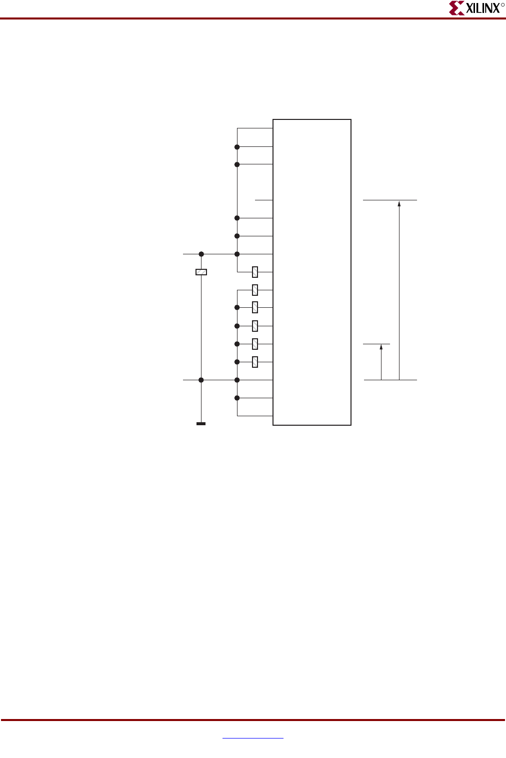
126 www.xilinx.com Virtex-5 FPGA ML561 User Guide
UG199 (v1.2) April 19, 2008
Appendix C: LCD Interface
R
Controller – Power Supply Circuits
Figure C-5 shows the power supply circuits. The power supply is used in the five times
boost mode, where VDD is 3.3V and VOUT is 16.5V. VOUT is the operating voltage of the
operational amplifier delivering the operating voltage, V0, for the LCD panel.
The LCD operating voltage, V0, is set with two resistors RA and RB. INTRS is driven Low
when the resistors are external. INTRS is driven High when the resistors are internal. For
the Virtex-5 FPGA ML561 Development Board, internal resistors are selected.
The LCD operating voltage (V0) and the Electronic Volume Voltage (VEV) can be calculated
in units of V using Equation C-1 and Equation C-2:
Equation C-1
Equation C-2
In Equation C-2, VREF is equal to 2.0V at 25 °C.
The values of the reference voltage parameter, α, and the ratio RA/RB are determined with
bit settings in the LCD controller’s instruction registers. Thus, it is possible to change
physical operating parameters of the LCD through register bit settings, controlling the
operating voltage, and the electronic volume level.
Figure C-5: Power Supply Circuits
DUTY1
DUTY2
BSTS
VR
MS
INTRS
17 VDD
18 VOUT
25
26
27
28
29
30 VSS1
2
1
VDD
VSS
VOUT
5 x VDD
VDD
VSS
16 VSS
DCDC5B
UG199_C_05_050106
V01
RB
RA
-------+
⎝⎠
⎛⎞
VEV
×=
VEV 163 α–
300
---------------–
⎝⎠
⎛⎞
VREF
×=
Virtex-5 FPGA ML561 User Guide www.xilinx.com 127
UG199 (v1.2) April 19, 2008
Hardware Schematic Diagram
R
The voltage and contrast settings must be configured before the LCD panel is ready for
operation. Figure C-6 shows the initialization procedure required to set up the LCD
controller.
Operation Example of the 64128EFCBC-3LP
The KS0713 LCD controller has several default settings of operation on the LCD panel
PCB. Some settings are forced through direct bonding on the chip. The default settings are:
•Master mode
•Parallel mode
•Internal oscillator
•Duty cycle ratio is set to 1/65
•Voltage converter input is between 2.4V ≤ VDD ≤ 3.6V, where VDD connects to 3.3V
•Internal voltage divider resistors
•Temperature coefficient is set to -0.05%/°C
•Normal power mode is set
Figure C-6: LCD Controller Initialization Flow
End Initialization
Regulator Resistor Select
Set Reference Voltage
FPGA Configured and Application Running
RESETB Pin is Taken HIGH
Start FPGA Configuration
RESETB Pin is Kept LOW
RESETB Pin is Kept LOW
Setup Instruction Flow
Wait longer than 1 ms between
each instruction to let the voltages stabilize.
The on-chip resistors are used.
Therefore, the selection MUST be
set to 101.
Setting Reference Voltage
is a two-pass instruction:
- Set Reference Voltage Mode
- Set Reference Voltage Register
LCD Bias
DUTY0, 1 is "11".
LCD Bias 0 = 1/7
LCD Bias 1 = 1/9
SHL Select
- SHL = 0 COM1 --> COM64
- SHL = 1 COM64 --> COM1
ADC Select
- ADC = 0 SEG1 --> SEG132
- ADC = 1 SEG132 --> SEG1
Board Power Supply Start
Power ON
Voltage Converter ON
Voltage Regulator ON
Voltage Follower ON
ADC Select
SHL Select
LCD Bias Select
UG199_C_06_050106
128 www.xilinx.com Virtex-5 FPGA ML561 User Guide
UG199 (v1.2) April 19, 2008
Appendix C: LCD Interface
R
•The voltage follower and voltage regulator are set to:
♦Five times boost mode
♦The V4, V3, V2, V1, and V0 outputs depend on the bias settings of 1/9 or 1/7.
Because of these default settings, the following display controller connections are not used:
•DISP: Turns into an output when Master mode is selected
•FRS: Static driver segment output
•M: Used in Master/Slave display configurations
•CL: Clock pin used in Master/Slave display configurations
When RESETB is Low, the display controller is initialized as indicated in Table C-3.
When RESETB is High, the display must be initialized. The first steps to be taken to
guarantee correct operation of the display and the controller are:
•Configure the ADC bit. This bit determines the scanning direction of the segments.
♦When the RESETB signal is active, ADC is reset to 0, meaning that the segments
are scanned from SEG1 up to SEG132.
♦When ADC is set to 1, the segments are scanned in opposite direction.
•Configure the SHL bit. This bit sets the scanning direction of the COM lines.
♦When the RESETB signal is active, SHL is reset to 0, meaning that the segments
are scanned from COM1 up to COM64.
♦When SHL is set to 1, the common lines are scanned in opposite direction.
Tab le C -3 : Display Controller Initialization (RESETB is Low)
Parameter Initial Value
Display OFF
Entire Display OFF
ADC Select OFF
Reverse Display OFF
Power Control 0,0,0 (VC, VR, VF)
LCD Bias 1/7
Read-Modify-Write OFF
SHL Select OFF
Static Indicator Mode OFF
Static Indicator Register 0,0 (S1, S0)
Display Start 0 (First line)
Column Address 0
Page Address 0
Regulator Select 0,0,0 (R2, R1, R0)
Reference Voltage OFF
Reference Voltage Register 1,0,0,0,0,0 (SV5, SV4, SV3, SV2, SV1, SV0)
Virtex-5 FPGA ML561 User Guide www.xilinx.com 129
UG199 (v1.2) April 19, 2008
Hardware Schematic Diagram
R
After the SHL bit is configured, these settings normally are not changed.
•Select the LCD bias settings.
♦The duty cycle is selected as 1/65 by hardwiring the controller IC pads on the
display PCB.
♦The LCD bias is set to:
-1/7: when the BIAS bit is 0
-1/9: when the BIAS bit is 1
The following steps are performed next:
•Start the onboard converter, regulator, and follower
•Set the regulator resistor values (see Table C-4)
•Configure the reference voltage register parameters (see Table C-5)
At startup of the LCD controller (after RESETB operation), the resistor and reference
voltage values are:
•Resistor selection is: 0,0,0
•Reference voltage is: 1,0,0,0,0,0
The resistor selection value MUST be set to 101b when using this LCD panel.
After the display is brought to operational mode, it is best to wait at least 1 ms to ensure the
stabilization of power supply levels. After this time, all other necessary display
initializations can be performed.
Tab le C -4 : Resistor Value Settings
3-Bit Data Settings (R2 R1 R0)
000 001 010 011 100 101 110 111
1+(Rb/Ra) 1.90 2.19 2.55 3.02 3.61 4.35 5.29 6.48
Tab le C -5 : Reference Voltage Parameters
SV5 SV4 SV3 SV2 SV1 SV0 Reference Voltage Parameter (α)
000000 0
000001 1
..
..
..
..
…
..
..
..
..
..
..
..
..
..
111110 62
111111 63

130 www.xilinx.com Virtex-5 FPGA ML561 User Guide
UG199 (v1.2) April 19, 2008
Appendix C: LCD Interface
R
Instruction Set
Table C-6 shows the instruction set for the LCD panel.
Table C-6: Display Instructions
Instruction RS RW DB7 DB6 DB5 DB4 DB3 DB2 DB1 DB0
Read display data 1 1 Read Data
8-bit data specified by the column and page address can be read from the Display Data RAM. The column address is increased automatically,
thus data can be read continuously from the addressed page.
Write display data 1 0 Write Data
8-bit data can be written into a RAM location specified by the column and page address. The column address is increased automatically, thus
data can be written continuously to the addressed page.
Read status 0 1 BUSY ADC ONOFF RESETB 0 0 0 0
BUSY: Device is BUSY when internal operation or reset. (0=active, 1 =busy).
ADC: Indicates the relationship between RAM column address and segment driver.
ONOFF: Indicates display ON or OFF status.
RESETB: Indicates if initialization is in progress.
Display ON/OFF001010111DON
Turn display ON or OFF. (1=ON, 0 = OFF)
Initial display line 0 0 0 1 ST5 ST4 ST3 ST2 ST1 ST0
Sets the line address of the display RAM to determine the initial line of the LCD panel.
ST5 ST4 ST3 ST2 ST1 ST0
000000Line address 0
000001Line address 1
.. .. .. .. .. .. ..
111110Line address 62
111111Line address 63
Set reference voltage mode0010000001
Set reference voltage register 0 0 x x SV5 SV4 SV3 SV2 SV1 SV0
This is a two-byte instruction. The first instruction sets the reference voltage mode. The second instruction sets the reference voltage parameter.
SV5 SV4 SV3 SV2 SV1 SV0
0000000
0000011
.. .. .. .. .. .. ..
11111062
11111163
Virtex-5 FPGA ML561 User Guide www.xilinx.com 131
UG199 (v1.2) April 19, 2008
Hardware Schematic Diagram
R
Set page address 0 0 1 0 1 1 P3 P2 P1 P0
This instruction sets the address of the display data page. Any RAM data bit can be accessed when its page address and column address are
specified. Changing the Page Address does not affect the display status.
P3 P2 P1 P0
0000page 0
0001page 1
.. .. .. .. ...
0111page 7
1000page 8
Set column address MSB 0 0 0 0 0 1 Y7 Y6 Y5 Y4
Set column address LSB 0 0 0 0 0 0 Y3 Y2 Y1 Y0
This instruction sets the address of the display data RAM. When a read or write to or from the display data RAM occurs, the addresses are
automatically increased.
Y7 Y6 Y5 Y4 Y3 Y2 Y1 Y0
00000000
Col
Addr 0
00000001
Col
Addr 1
.. .. .. .. .. .. .. .. ...
11111110
Col
Addr
130
11111111
Col
Addr
131
ADC select 0 0 1 010000ADC
This instruction changes the relationship between RAM column address and segment driver.
ADC = 0, SEG1 --> SEG132 default mode
ADC = 1, SEG132 --> SEG1
Table C-6: Display Instructions (Continued)
Instruction RS RW DB7 DB6 DB5 DB4 DB3 DB2 DB1 DB0
132 www.xilinx.com Virtex-5 FPGA ML561 User Guide
UG199 (v1.2) April 19, 2008
Appendix C: LCD Interface
R
Reverse display ON/OFF001010011REV
REV RAM bit data = '1' RAM bit data = '0'
0 Pixel ON Pixel OFF
1 Pixel OFF Pixel ON
Entire display ON/OFF001010010EON
This instruction forces the display to be turned on regardless the contents of the display data RAM. The contents of the display data RAM are
saved. This instruction has priority over reverse display.
LCD bias select 0 0 1 010001BIAS
This instruction selects the LCD bias.
Duty
ratio Bias = 0 Bias = 1
1/65 1/7 1/9
Set modify-read 0011100000
This instruction stops the automatic incrementing of the column address by a read operation. The automatic increment is still done with a
write operation.
Reset modify-read0011101110
This instruction resets the changed modify-read to the normal.
Reset 0011100010
This instruction resets the LCD controller registers to the default values. The instruction CANNOT initialize the LCD power supply initialized
with RESETB.
SHL select 0 0 1 1 0 0 SHL x x x
This instruction sets the COM output scanning direction.
SHL = 0, COM1 ----> COM64 (default)
SHL = 1, COM64 ----> COM1
Power Control 0000101VCVRVF
This instruction selects one of the eight power circuit functions. In the case of the DisplayTech 64128EFCBC display, these must be kept at "000"
Regulator resistor select 0 0 0 0100R2R1R0
This instruction selects the resistor ratio Rb/Ra.
Set static indicator mode001010110SM
Set static indicator register00xxxxxxS1S0
This is a two-byte instruction. The first instruction enables the second instruction. The second instruction update the contents of the static
indicator register.
Table C-6: Display Instructions (Continued)
Instruction RS RW DB7 DB6 DB5 DB4 DB3 DB2 DB1 DB0
Virtex-5 FPGA ML561 User Guide www.xilinx.com 133
UG199 (v1.2) April 19, 2008
Hardware Schematic Diagram
R
Read/Write Characteristics (6800 Mode)
Table C-7 list the read and write timing parameters in 6800 mode. The associated
waveforms for these parameters are illustrated in Figure C-7.
Tab le C -7 : Read/Write Characteristics in 6800 Mode
Parameter Signal Symbol Min Typ Max Unit
Address Setup Time RS TAS 13 - - ns
Address Hold Time TAH 17 - - ns
Data Setup Time DB7 to DB0 TDS 35 - - ns
Data Hold Time TDH 13 - - ns
Access Time TACC - - 125 ns
Output Disable Time TOD 10 - 90 ns
System Cycle Time RS TCYC 400 - - ns
Enable Pulse Width Read/Write E_RD TPWR 125 - ns
TPWW 55 - ns
Figure C-7: Read/Write Timing Waveforms (6800 Mode)
RS
RW
CS1B
E
WRITE
DB0-DB7
READ
UG199_C_07_050106
TASTAH
TCYC
TPWR
TACC TOD
TPWW
TDSTDH

134 www.xilinx.com Virtex-5 FPGA ML561 User Guide
UG199 (v1.2) April 19, 2008
Appendix C: LCD Interface
R
Design Examples
LCD Panel Used in Full Graphics Mode
The LCD controller RAM has eight 132-byte pages (in fact, there are nine pages; page 9 is
special). Each page is one byte wide. If all the pages are put in one memory block, the
needed space is 8 pages x 8 bits x 132 pixels or 8448 bits (1056 bytes).
One Virtex-5 FPGA block RAM can be configured as 8+1 by 2048.
One block RAM can be used to store one complete pixel view of the LCD panel. There is
enough space left for commands.
The ninth bit in the block RAM indicates whether the data in the block RAM is real data to
be displayed or is a command for the controller.
The interface to the LCD panel is slow. The E signal can be used as the controller clock
signal. This signal has a minimum cycle time of 400 ns for displaying 8 bits (equal to 8 dots)
on the LCD. One full page of the display takes up to 132 x 400 ns = 52.8 μs. Updating the
full display takes 52.8μs x 8 = 423μs.
If using the dual port and data width capabilities of the block RAM, then writes to the
block RAM can be 32 bits (+4 control bits), and reads from the block RAM on the LCD side
can be 8 bits (1 control bit). An entire LCD page is updated in 33 write operations.
The interface on the LCD panel side sequentially reads the block RAM, and thus, updates
the screen contiguously (like a television screen). The controller (microcontroller or other)
side of the block RAM can be written at any time.
The write operation happens on the rising edge of the clock and the read (LCD update)
happens on the falling edge of the clock. Normally write and read operations at the same
address give corrupt read data when the read and write clock edges do not respect the
clock-to-clock setup timing. This problem is solved by using both edges of the clock.
A state machine provides correct timing of the signals on the LCD panel side. The panel
can be used in write-only mode or in read/write mode. Most of the time, LCD panels
operate in write-only mode.
At first, the block RAM must be initialized with some data (instructions to the LCD) to
make the LCD operate correctly. Figure C-8 illustrates a general block diagram of the LCD
panel in full graphics mode.
Virtex-5 FPGA ML561 User Guide www.xilinx.com 135
UG199 (v1.2) April 19, 2008
Hardware Schematic Diagram
R
LCD Panel Used in Character Mode
This design example requires a byte representing a command or data to be displayed as
input.
•When the Enable signal is Low, nothing happens. The display interface design is
locked.
•When the Enable signal is High and the data_or_command control signal is Low, the
byte written is a display command.
•When the Enable signal and the data_or_command control signal are High, the byte
written is the ASCII character code of the character to be put on the display.
Display Command Byte
The command set of the display can be found in Table C-6, page 130.
When the LCD interface is enabled for the first time, a set of command bytes is sent to the
LCD. This command set provides the basic initialization of the LCD controller. When this
initialization is done, the normal LCD interface is freed for normal use. Command bytes
from the valid command set can be sent to the display (controller).
The Toplevel.vhd.txt file provides a detailed description of the LCD controller
interface.
Figure C-8: General Block Diagram of LCD Panel in Full Graphics Mode
UG199_C_08_050106
Block RAM
IorD = '1' Instruction
'0' Data
Design for Full Graphics Interface, Attached to CoreConnect Bus
Enable
Write
Address
WData (32+4)
RData (8+gnd)
ena
Clock
read
Addr
IorD (bit 9)
DataIn (8)
DataOut (8)
RW
E
Clock
Reset
Clock
Reset
Clock
E
TC
RS
CS1B
DB (8)
CoreConnect
State
Machine
Clock
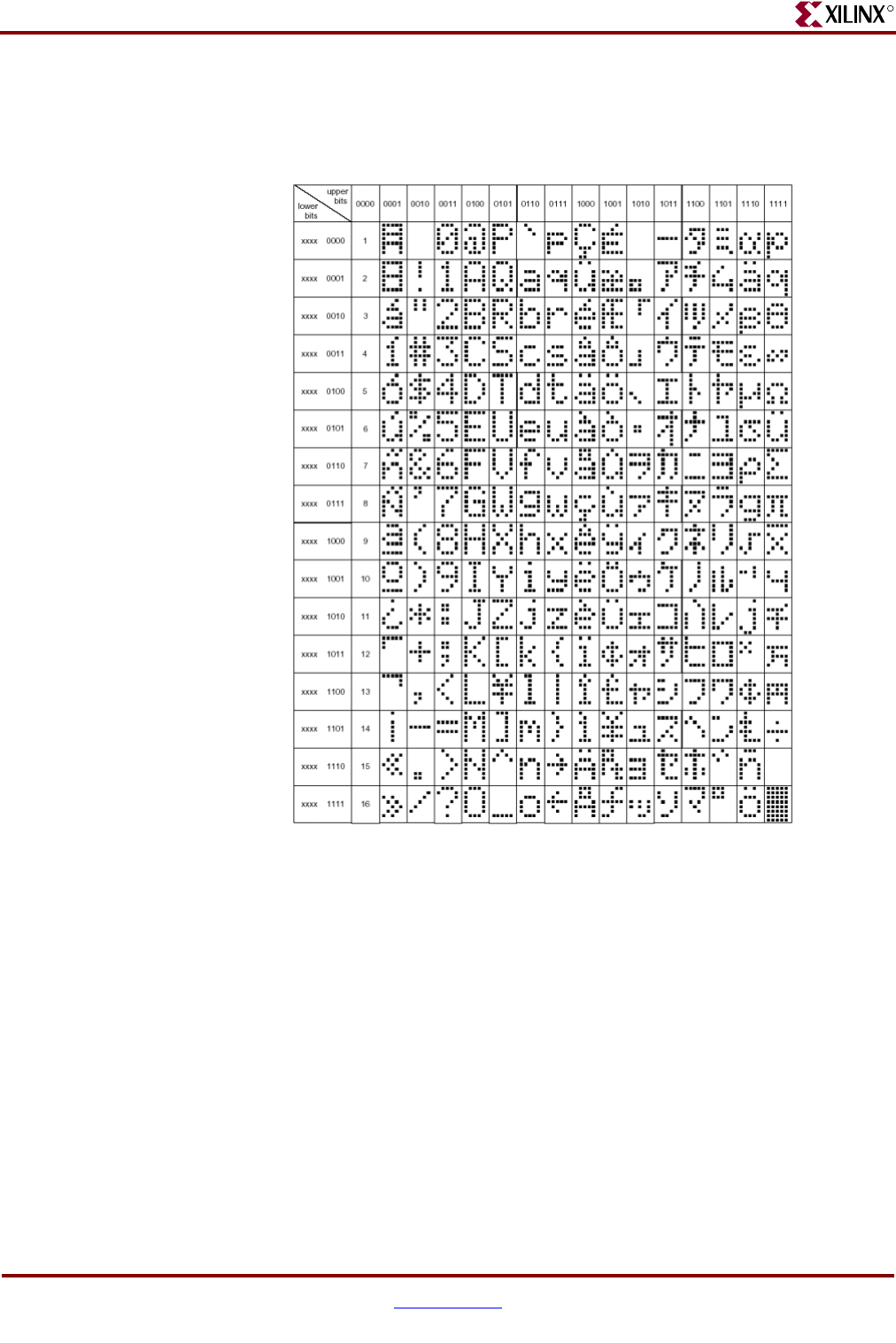
136 www.xilinx.com Virtex-5 FPGA ML561 User Guide
UG199 (v1.2) April 19, 2008
Appendix C: LCD Interface
R
Display Data Byte
The supplied byte must be a valid ASCII representation of a character as shown in
Figure C-9.
The character set is stored in block RAM (used as ROM). The CharacterSet.xls file
contains the layout of the block RAM character set. The block RAM (see Figure C-10) is
organized as small arrays of eight bytes, which is easy for address calculation.
Figure C-9: ASCII Character Representations
UG199_C_09_050106
Virtex-5 FPGA ML561 User Guide www.xilinx.com 137
UG199 (v1.2) April 19, 2008
Hardware Schematic Diagram
R
When presenting byte value 30 hex, character 0 must be displayed. Shifting the value
00110000b (30h) up three positions gives the value 180h or 348d.
Because each character uses eight byte locations, character 0 in the character set starts from
memory location 348 decimal.
For example, character X has byte value 58h or 01011000b. Shifting this value three
positions gives the value 2C0h or 704d.
Figure C-10: Block RAM Organization
F0 - FF
The RAM array is divided in
pages of eight bytes by 16,
forming an array of 128 bytes.
This array represents one
column of standard ASCII table.
A character is stored as:
E0 - EF
D0 - DF
C0 - CF
B0 - BF
A0 - AF
Not Used
Not Used
70 - 7F
60 - 6F
50 - 5F
40 - 4F
30 - 3F
20 - 2F
10 - 1F
Not Used
2047
1280
1279
1024
1023
N-x
N
N-1 Shift
Direction
Addr
0
01234567 Data
256
255
0
Addr[10:0]
Data[7:0]
RAMB16_S9
UG199_C_10_050106
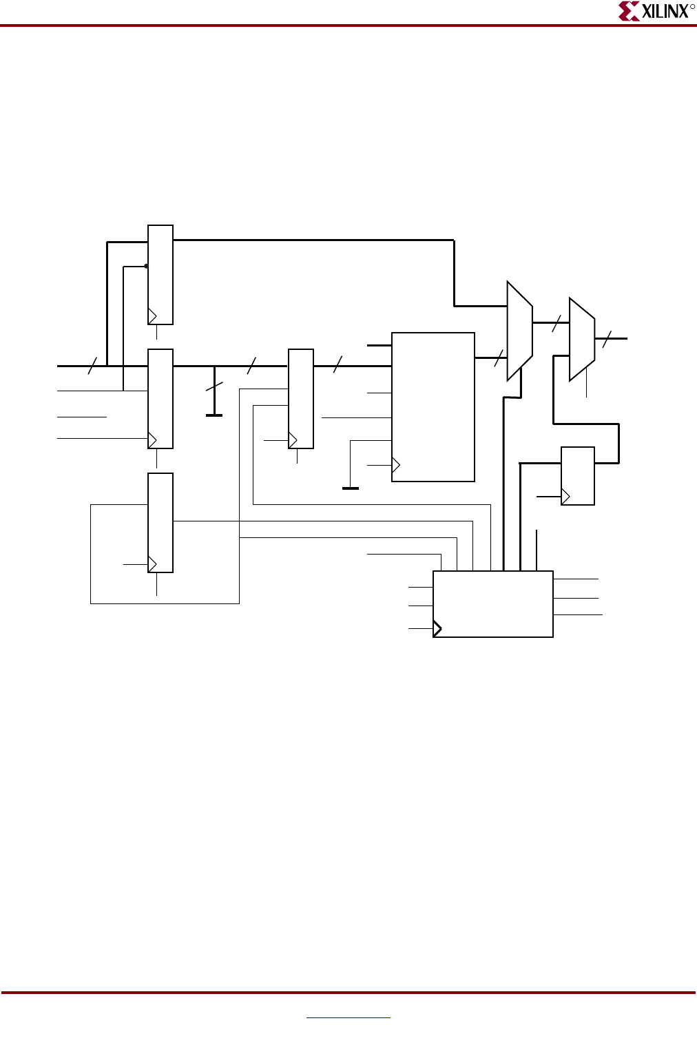
138 www.xilinx.com Virtex-5 FPGA ML561 User Guide
UG199 (v1.2) April 19, 2008
Appendix C: LCD Interface
R
Figure C-11 shows a block diagram of the LCD character generator controller. Character
data is latched and then shifted left three positions. This shifted value is the start byte for a
counter that outputs an address to the block RAM. The result is a stream of bytes
representing a character for the display.
A small second counter determines when a new character is loaded into the block RAM
address counter.
A state machine manages the processing order.
A minimum cycle time of 400 ns on the E signal used as a reference. The 200 MHz system
clock frequency is used as reference system clock. One E cycle uses at least 80 system clock
cycles when the design is running at 200 MHz. The E pulse is part of the state machine, and
the design only depends on the system clock. Timing is met as long as the system clock
does not exceed 200 MHz.
This design can be adapted easily to fit the MicroBlaze™ or PPC405 CoreConnect bus
system.
Figure C-11: LCD Character Generator Controller
TC
L
Addr
DI
E E
RAMB16_S9
Counter B
Counter A
Position
Register
Clk
Ena
DataIn
Ena
E Load
Clk
Clk
Clk
We
DO
Ssr
8
3
11 11 8
Count to 8.
Stop both counters at TC.
Send character position and
line to the LCD.
Load new value in counter A.
Switch to character ROM.
Enable counters.
8
Clk
Ena State Machine
Page
Rst
Rst
Display
Register
DesRst
DesRst DesRst
DesRst
DesRst
DesRst
8
Clk
LUT-ROM
Display
Initialization
RS
RW
Data
E
1
0
UG199_C_11_050106
Virtex-5 FPGA ML561 User Guide www.xilinx.com 139
UG199 (v1.2) April 19, 2008
Hardware Schematic Diagram
R
Array Connector Numbering
Figure C-12 shows the LCD connections for Bank 0.
Figure C-12: LCD Connections (Bank 0)
Bank 0
Connector Pin
ABCDE FGH I D9 LCD_D0
10 D7 LCD_D4
9D5 LCD_D5
8D3 LCD_D6
7D1 LCD_D7
6E10 LCD_RST
5E8LCD_D1
4E6 LCD_D2
3E4 LCD_D3
2E2 LCD_ENA
1F5 LCD_R/W
F3 LCD_RSEL
Connector J32 F1 LCD_CS1B
UG199_C_12_050106

