Xircom An Intel GEM3501 Core Engine, PCS-1900 GSM Radio Module User Manual Core Engine Developer Guide
Xircom, An Intel Company Core Engine, PCS-1900 GSM Radio Module Core Engine Developer Guide
Contents
- 1. Core Engine Approvals Guide
- 2. Core Engine Developers Guide
Core Engine Developers Guide
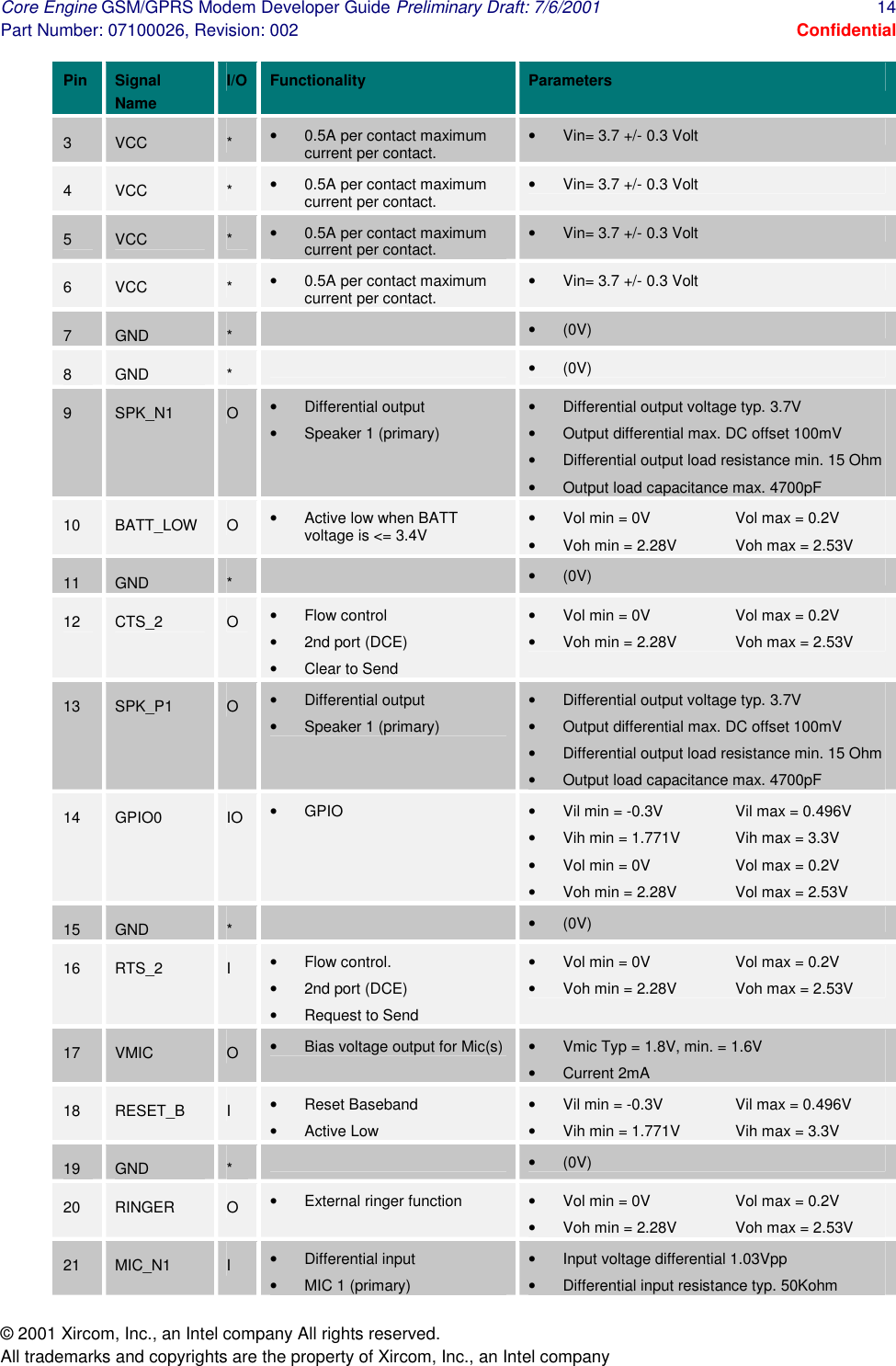
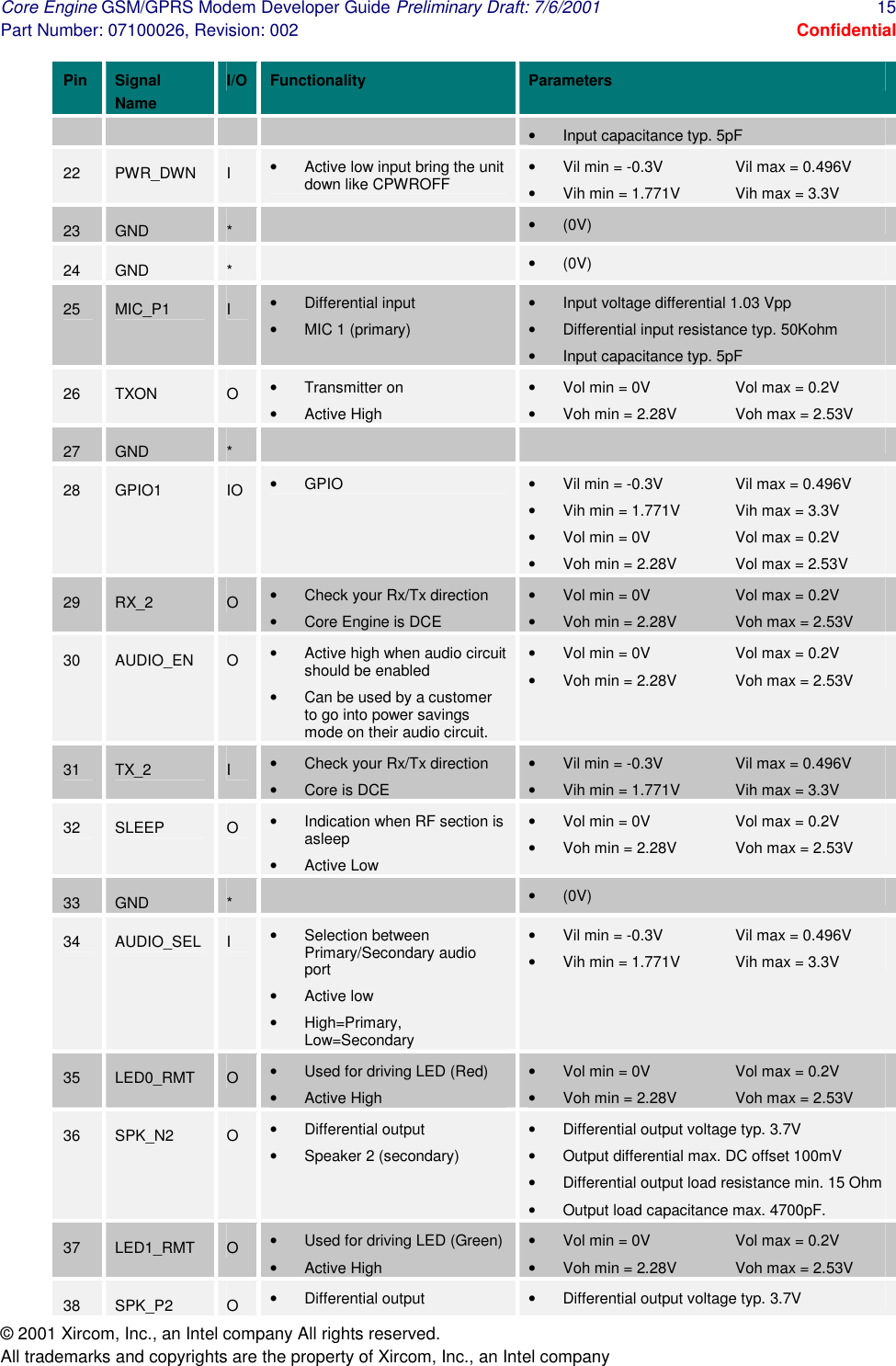
![Core Engine GSM/GPRS Modem Developer Guide Preliminary Draft: 7/6/2001 5 Part Number: 07100026, Revision: 002 Confidential © 2001 Xircom, Inc., an Intel company All rights reserved. All trademarks and copyrights are the property of Xircom, Inc., an Intel company TTAABBLLEE OOFF CCOONNTTEENNTTSS 1 REVISION HISTORY ....................................................................................................2 2 SAFETY PRECAUTIONS.............................................................................................3 2.1 Important Safety Information........................................................................................ 3 2.2 Guidelines for Limiting RF Exposure............................................................................ 3 2.3 Disclaimer.................................................................................................................... 3 2.4 Beta Release Notes..................................................................................................... 4 2.4.1 Data Services....................................................................................................... 4 2.4.2 AT Commands..................................................................................................... 4 2.4.3 PUK Procedure.................................................................................................... 4 3 PRODUCT OVERVIEW................................................................................................9 3.1 GSM Overview ............................................................................................................ 9 3.2 Model Variation............................................................................................................ 9 3.3 General Description..................................................................................................... 9 3.4 Summary of the Features for the Core Engine modem...............................................10 3.5 Programmer Reference ..............................................................................................10 3.6 Backward Compatibility...............................................................................................10 3.7 Modes of Operation ....................................................................................................11 3.7.1 Circuit Switched Data..........................................................................................11 3.7.2 Transparent and Non Transparent Transmissions...............................................11 3.7.3 Short Message Service .......................................................................................11 3.7.4 Voice...................................................................................................................12 3.7.5 General Packet Radio Service (GPRS)...............................................................12 4 CARRIER BOARD......................................................................................................13 4.1 Core Engine Modem I/O Interface [P4] .......................................................................13 4.2 Core Engine I/O Signal Header [J4]............................................................................17 4.3 Ground Points [J2, J9] ................................................................................................17 4.4 RF Antenna Connector [J5, J6]...................................................................................17 4.5 Power [J7, J8, J10] ....................................................................................................17 4.6 Primary Serial Interface [P3] .......................................................................................18](https://usermanual.wiki/Xircom-An-Intel/GEM3501.Core-Engine-Developers-Guide/User-Guide-167161-Page-5.png)
![Core Engine GSM/GPRS Modem Developer Guide Preliminary Draft: 7/6/2001 6 Part Number: 07100026, Revision: 002 Confidential © 2001 Xircom, Inc., an Intel company All rights reserved. All trademarks and copyrights are the property of Xircom, Inc., an Intel company 4.7 Secondary Serial Interface [P2] ..................................................................................18 4.8 Primary Audio Interface [P1].......................................................................................19 4.9 Secondary Audio Interface [J1]...................................................................................20 4.10 Audio Interface Select [JP2]......................................................................................20 4.11 Subscriber Interface Module [J3] ..............................................................................20 4.12 Status Indication [DS1] .............................................................................................20 5 POWER.......................................................................................................................22 5.1 Power Up Sequence...................................................................................................22 5.2 Power Management....................................................................................................22 5.2.1 Power Modes......................................................................................................22 5.2.2 Hardware Signals................................................................................................24 5.2.3 Software Commands...........................................................................................24 5.3 Transmit Power ..........................................................................................................25 6 SERIAL COMMUNICATIONS ....................................................................................26 6.1 Supported Serial Port Configurations..........................................................................26 6.1.1 Single Port Configuration ....................................................................................26 6.1.2 Dual Port Configuration.......................................................................................27 7 AUDIO.........................................................................................................................29 7.1 Audio Path Selection ..................................................................................................29 7.1.1 Hardware Selection of Audio Path.......................................................................29 7.1.2 Software Selection of Audio Path........................................................................29 7.2 Microphone Input........................................................................................................29 7.3 Speaker Output ..........................................................................................................30 7.4 Audio Circuit Implementation......................................................................................31 7.4.1 Example Single-Ended Microphone Circuit .........................................................31 7.4.2 Example Differential Microphone Circuit..............................................................32 7.5 Microphone Cable Considerations..............................................................................32 8 RF ANTENNA.............................................................................................................33 8.1 Antenna Connector.....................................................................................................33 8.2 Antenna Selection.......................................................................................................33 8.3 Antenna Performance Guidelines ...............................................................................33 8.3.1 Antenna Impedance Match .................................................................................33 8.3.2 Antenna Pattern and Gain...................................................................................34 8.3.3 Antenna Beam Width ..........................................................................................34](https://usermanual.wiki/Xircom-An-Intel/GEM3501.Core-Engine-Developers-Guide/User-Guide-167161-Page-6.png)
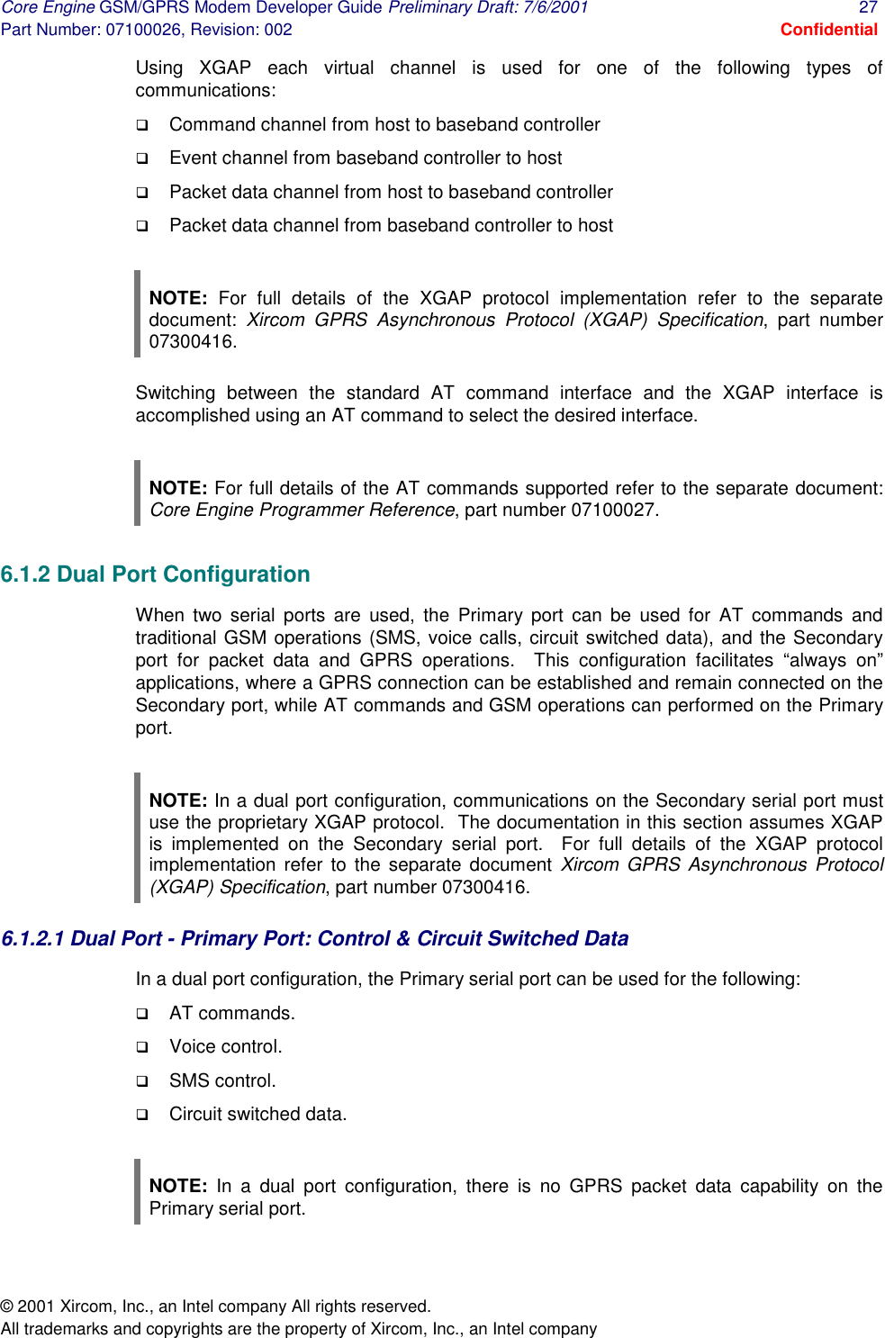
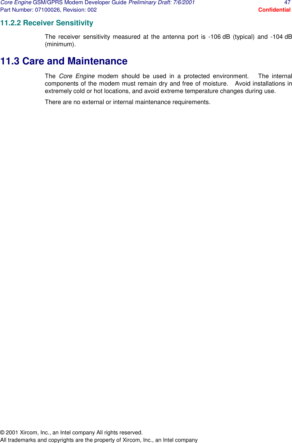
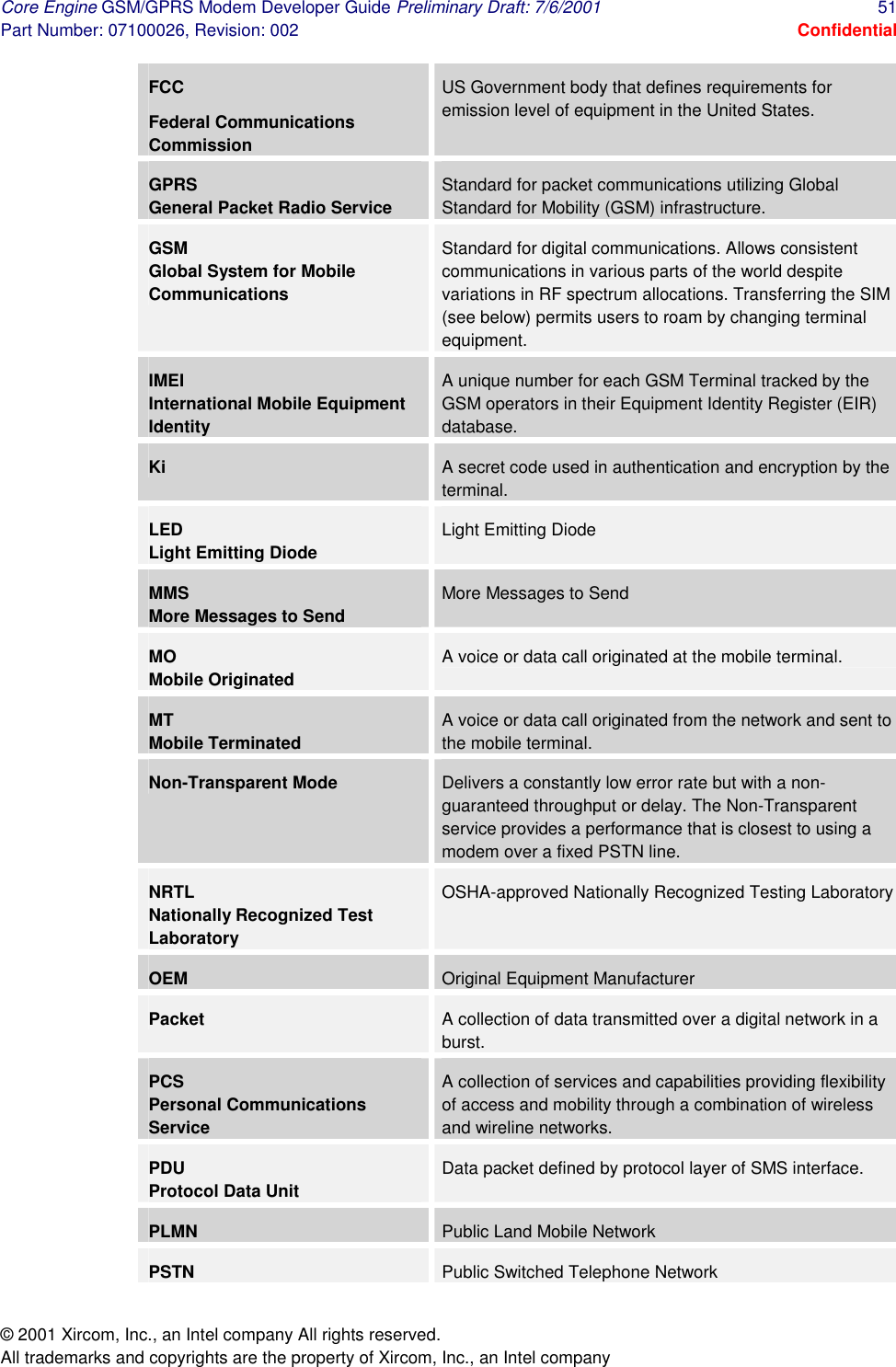
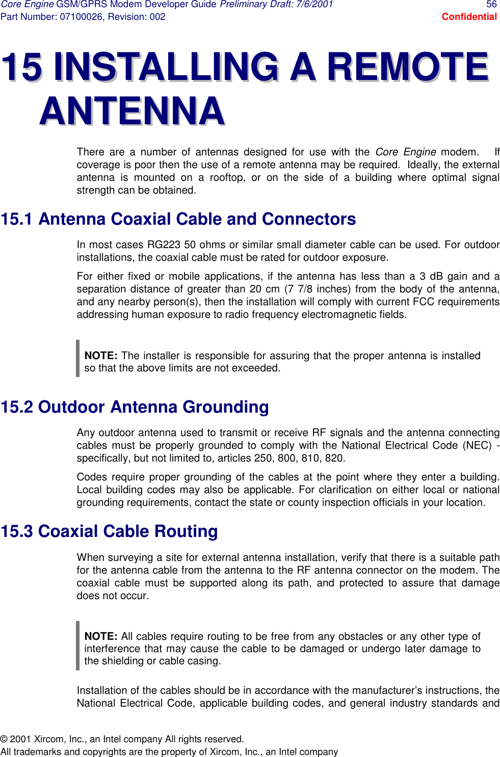
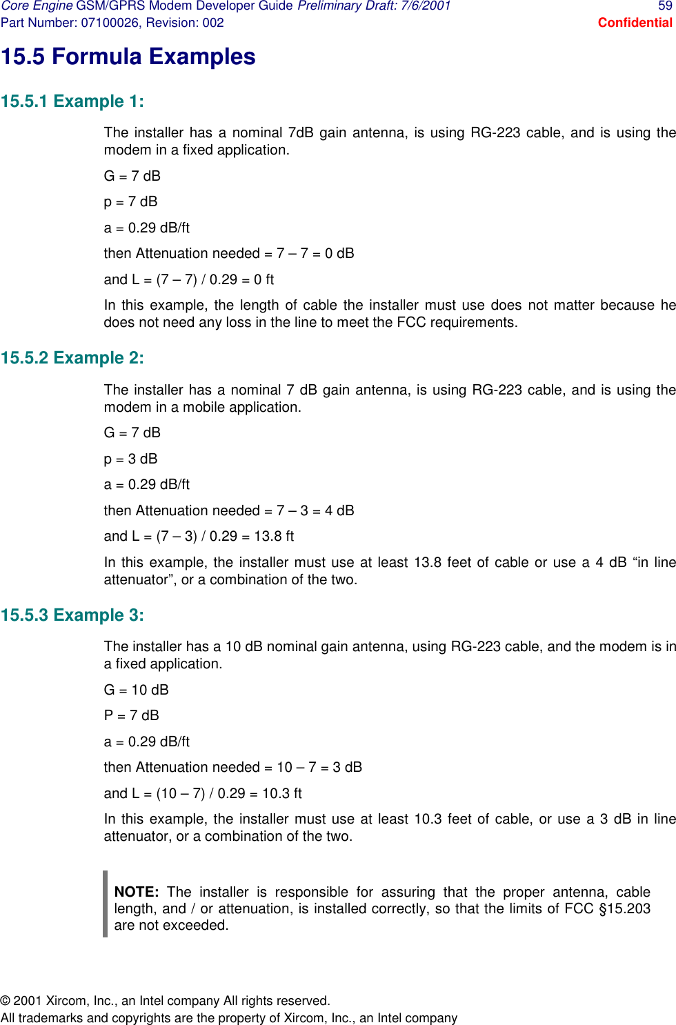
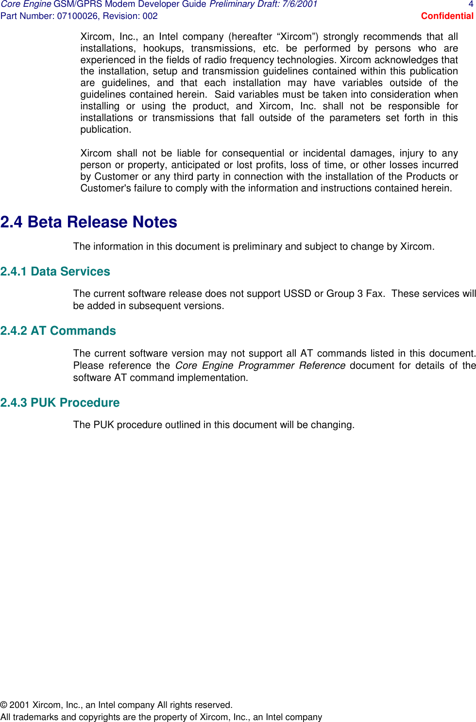
![Core Engine GSM/GPRS Modem Developer Guide Preliminary Draft: 7/6/2001 13 Part Number: 07100026, Revision: 002 Confidential © 2001 Xircom, Inc., an Intel company All rights reserved. All trademarks and copyrights are the property of Xircom, Inc., an Intel company 44 CCAARRRRIIEERR BBOOAARRDD Figure 1: Core Engine Carrier Board (Rev B) NOTE: The carrier board is intended for development only, and is not suitable for performing RF qualification. 4.1 Core Engine Modem I/O Interface [P4] The Core Engine modem connects to the carrier board using a 60-pin connector (connector P4 on the carrier board). The I/O interface signals are described in Table 2. Pin Signal Name I/O Functionality Parameters 1 VCC * • 0.5A per contact maximum current per contact. • Vin= 3.7 +/- 0.3 Volt 2 VCC * • 0.5A per contact maximum current per contact. • Vin= 3.7 +/- 0.3 Volt [P4] Core Engine I/O connector.[J3] SIM holder. [JP2] Audio port select jumper. [P2] DB-9 for secondary serial port. [P3] DB-9 for primary serial port. [J7, J8, J10] Power 3.7V (+/-0.3V). [DS1] Status LED. [J5] Connector for cable to Core Engine RF antenna connector. [P1] RJ-9 for primary audio port (differential). [J4] Header access to Core Engine I/O pins. [J6] SMA RF antenna connector. [J1] Secondary audio port (single-ended). [J2, J9] GND ref points.](https://usermanual.wiki/Xircom-An-Intel/GEM3501.Core-Engine-Developers-Guide/User-Guide-167161-Page-13.png)
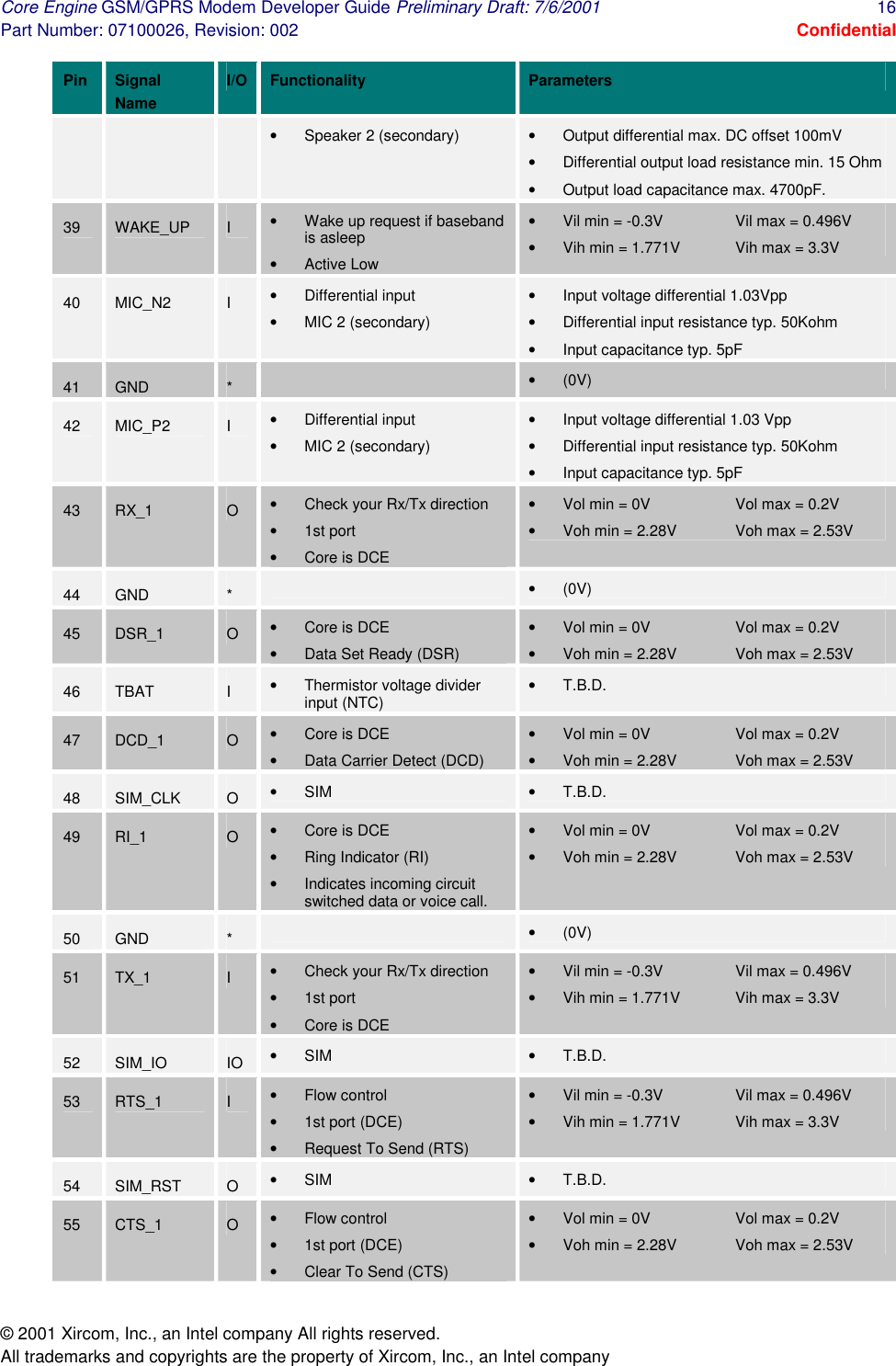
![Core Engine GSM/GPRS Modem Developer Guide Preliminary Draft: 7/6/2001 17 Part Number: 07100026, Revision: 002 Confidential © 2001 Xircom, Inc., an Intel company All rights reserved. All trademarks and copyrights are the property of Xircom, Inc., an Intel company Pin Signal Name I/O Functionality Parameters 56 SIM_GND O • SIM • GND 57 DTR_1 I • Core is DCE • Data Terminal Ready (DTR) • Vil min = -0.3V Vil max = 0.496V • Vih min = 1.771V Vih max = 3.3V 58 SIM_VCC O • SIM • T.B.D. 59 GND * • (0V) 60 GND * • (0V) Table 2: Core Engine I/O Connector Pin Out 4.2 Core Engine I/O Signal Header [J4] The Core Engine I/O signals can be accessed externally at a 60-pin header (connector J4 on the carrier board). The I/O interface signals are described in Table 2. 4.3 Ground Points [J2, J9] Two ground points are provided (J2 and J9 on the carrier board) which can be used for any probe hookup, for example to an oscilloscope. 4.4 RF Antenna Connector [J5, J6] The RF antenna may be connected to the Core Engine modem directly, or to the carrier board (at connector J6). When connecting the RF antenna to the carrier board, a cable must also be connected from the carrier board (at connector J5) to the RF connector on the Core Engine board. The Core Engine board uses a muRata Microminiature SMT Coaxial Connector (muRata p/n “MM9329-2700”) for RF antenna connection. The carrier board uses an SMA connector for connection to an antenna, and a muRata Microminiature SMT Coaxial Connector (muRata p/n “MM9329-2700”) for connection to the Core Engine board RF connector. The Core Engine modem is designed to support interchangeable antenna types, provided that each antenna has 50-ohm impedance and has been tuned to the frequency band intended. 4.5 Power [J7, J8, J10] The Core Engine carrier board requires an input voltage of 3.7 VDC +/- 0.3V (connectors J7, J8 & J10 on the carrier board). CAUTION: The carrier board powers the Core Engine board directly, and so must be used with a 3.7V (+/- 0.3V) power supply only.](https://usermanual.wiki/Xircom-An-Intel/GEM3501.Core-Engine-Developers-Guide/User-Guide-167161-Page-17.png)
![Core Engine GSM/GPRS Modem Developer Guide Preliminary Draft: 7/6/2001 18 Part Number: 07100026, Revision: 002 Confidential © 2001 Xircom, Inc., an Intel company All rights reserved. All trademarks and copyrights are the property of Xircom, Inc., an Intel company 4.6 Primary Serial Interface [P3] The primary serial I/O interface (connector P3 on the carrier board) implements RS-232 using a DB-9 connector and supports auto baud capability from 2400 bps to 115200 bps with hardware handshake flow control. Pin Number Signal Name Direction Functionality 1 DCD0_DS To CPE Data Carrier Detect 0. DCE Output signal. Active low. Main serial interface data carrier detect signal. Connects to a DTE, CD, Carrier Detect pin. 2 RX0_DS To CPE Receive data 0. DCE Output signal. Main serial interface transmit data signal. During idle or reset, signal will be a logic 1. Connects to a DTE, RX, receive data pin. 3 TX0_DS From CPE Transmit data 0. DCE Input signal. Active low. Main serial interface receive data signal. During idle or reset, signal will be a logic 1. Connects to a DTE, TX, transmit data pin. 4 DTR0_DS From CPE Data Terminal Ready 0. DCE Input signal. Active low. Main serial interface data terminal ready signal. Connects to a DTE, DTR, Data Terminal Ready pin. 5 GND_IN From CPE Electrical power return for digital and analog grounds. 6 DSR0_DS To CPE Data Set Ready 0. DCE Output signal. Active low. Main serial interface data set ready signal. Connects to a DTE, DSR, Data Set Ready pin. 7 RTS0_DS From CPE Request-To-Send 0. DCE Input signal. Active low. Main serial interface request to send signal. Connects to a DTE, RTS, Request-To-Send pin. 8 CTS0_DS To CPE Clear-To-Send 0. DCE Output signal. Active low. Main serial interface clear to send signal. Connects to a DTE, CTS, Clear to send pin. 9 RI0_DS To CPE Ring Indicator 0. DCE Output signal. Active low. Main serial interface ring indicator signal. Connects to a DTE, RI, Ring Indicator pin. Table 3: Carrier Board Primary Serial Connector Pin Out NOTE: The maximum length for the Primary Serial cable is 25 feet. 4.7 Secondary Serial Interface [P2] The secondary serial I/O interface (connector P2 on the carrier board) implements RS-232 using a DB-9 connector and supports auto baud capability from 2400 bps to 115200 bps with hardware handshake flow control. Pin Number Signal Name Direction Functionality](https://usermanual.wiki/Xircom-An-Intel/GEM3501.Core-Engine-Developers-Guide/User-Guide-167161-Page-18.png)
![Core Engine GSM/GPRS Modem Developer Guide Preliminary Draft: 7/6/2001 19 Part Number: 07100026, Revision: 002 Confidential © 2001 Xircom, Inc., an Intel company All rights reserved. All trademarks and copyrights are the property of Xircom, Inc., an Intel company Pin Number Signal Name Direction Functionality 2 RX0_DS To CPE Receive data 0. DCE Output signal. Main serial interface transmit data signal. During idle or reset, signal will be a logic 1. Connects to a DTE, RX, receive data pin. 3 TX0_DS From CPE Transmit data 0. DCE Input signal. Active low. Main serial interface receive data signal. During idle or reset, signal will be a logic 1. Connects to a DTE, TX, transmit data pin. 7 RTS0_DS From CPE Request-To-Send 0. DCE Input signal. Active low. Main serial interface request to send signal. Connects to a DTE, RTS, Request-To-Send pin. 8 CTS0_DS To CPE Clear-To-Send 0. DCE Output signal. Active low. Main serial interface clear to send signal. Connects to a DTE, CTS, Clear to send pin. Table 4: Carrier Board Secondary Serial Connector Pin Out NOTE: The maximum length for the Secondary Serial cable is 25 feet. 4.8 Primary Audio Interface [P1] The primary audio interface (connector P1 on the carrier board) uses an RJ-9 connector and provides differential microphone input and speaker output. Pin Number Signal Name Direction Functionality 1 MIC0N From CPE Microphone Negative. Negative input pin from an electret-type microphone. Nominal microphone differential voltage should be 2.0 volts. Impedance not less than 900 ohms. Leave signal disconnected if function is not used. 2 SPK0N To CPE Speaker Negative. Negative output pin. Low side of a push-pull amplifier. Speaker impedance 15 ohms, minimum. Speaker capacitance of 700 pF, maximum. Driver voltage is 3.7V peak-to-peak. Leave signal disconnected if function is not used. 3 SPK0P To CPE Speaker Positive. Positive output pin. High side of a push-pull amplifier. Speaker impedance 15 ohms, minimum. Speaker capacitance of 700 pF, maximum. Driver voltage is 3.7V peak-to-peak. Leave signal disconnected if function is not used. 4 MIC0P From CPE Microphone Positive. Positive input pin from an electret-type microphone. Nominal microphone differential voltage should be 2.0 volts. Impedance not less than 900 ohms. Leave signal disconnected if function is not used. Table 5: Carrier Board Primary Audio Port Connector Pin Out](https://usermanual.wiki/Xircom-An-Intel/GEM3501.Core-Engine-Developers-Guide/User-Guide-167161-Page-19.png)
![Core Engine GSM/GPRS Modem Developer Guide Preliminary Draft: 7/6/2001 20 Part Number: 07100026, Revision: 002 Confidential © 2001 Xircom, Inc., an Intel company All rights reserved. All trademarks and copyrights are the property of Xircom, Inc., an Intel company 4.9 Secondary Audio Interface [J1] The secondary audio interface (connector J1 on the carrier board) provides single-ended microphone input and speaker output. 4.10 Audio Interface Select [JP2] Selection of which audio interface is active is controlled by a jumper (jumper JP2 on the carrier board). If the jumper is removed, the primary audio interface is active; if the jumper is installed, the secondary audio interface is active. This jumper is in parallel with the audio select pin (‘AUDIO_SEL’) on the Core Engine I/O connector. 4.11 Subscriber Interface Module [J3] The SIM, an integral part of any GSM terminal device, is programmed with subscriber information. The SIM is not provided with the Core Engine unit and must be provided by the GSM service subscriber. Care must be taken to protect the SIM. A GSM terminal will not operate without the SIM installed. The user information consists of an identity (IMSI number) registered with the GSM provider, and an encryption Ki (pronounced key). The SIM consists of a microprocessor chip and memory, installed on a plastic card. Core Engine uses the "mini-SIM" or plug in configuration. The SIM, which is removable, installs in a holder (connector J3) on the carrier board. The SIM card performs authentication. To gain access to the GSM network, the network must recognize the IMSI number and the terminal must be able to properly decrypt the data sent by the network. The SIM also serves as a buffer for Incoming and Stored SMS messages, or when a radio link is not available, store an outgoing message until a network link is established. NOTE: Power must be off when installing or removing a SIM card. 4.12 Status Indication [DS1] The Core Engine carrier board provides a multi-color LED (DS1 on the carrier board) that indicates the current link status and signal quality. NOTE: The LED illuminates any time power is applied to the carrier board. LED Color Link Status Green Modem is attached to the network Flashing Orange Modem is registered on the network but is rejected Flashing Red Modem is in Start-up mode or is not attached to the network Table 6: Carrier Board LED Colors](https://usermanual.wiki/Xircom-An-Intel/GEM3501.Core-Engine-Developers-Guide/User-Guide-167161-Page-20.png)