YEONHWA M TECH TD-2400MD Zigbee Data Modem Module User Manual
YEONHWA M TECH CO.,LTD Zigbee Data Modem Module
UserManual.wiki
>
YEONHWA M TECH
>
TD 2400MD User Manual
USER MANUAL
Navigation menu
Upload a User Manual
Namespaces
Wiki Guide
HTML
PDF
Info
Views
User Manual
Discussion / Help
Navigation
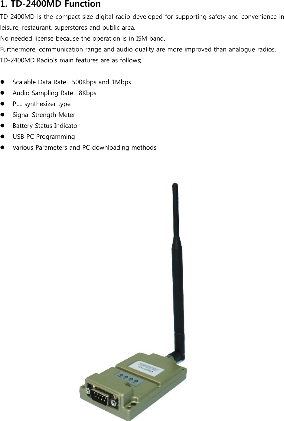
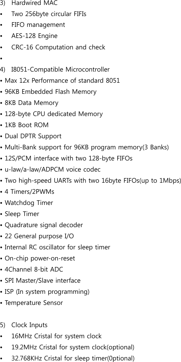
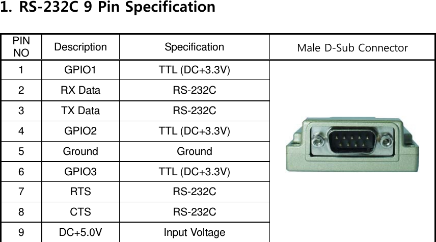
![Circuit Description TD-2400MD digital radio is consisted of RF module included MG2455, RF AMP to amplify output power, LED Display that shows condition of drive chip and Data modem which supports RS-232C after transforming from Digital signal into serial signal. 1. MG2455 ZigBee Chip and peripheral components MG2455(U11) is the RF module operated in 2.4Ghz ISM band. The module is made with RF transceiver, RF circuit, 8051 compatible MCU and several components. It follows IEEE802.15.4 and Zigbee standard regulation. MG2455 includes zigbee stack library as zPULSE. LM2455 data rate is from 250Kbps to 1Mbps available. Reset circuit is consisted of Q14, R38 and C52 and operates when the voltage is below 2.5V. Port P0.1, P0.2, P0.3is used as LED Display Port that shows TD-2400MD performance. Port P0[5] and P0[6] are connected to EEPROM(U14) for current status restore. P3[5], P3[6] and P3[7] are for GPIO control. LM2455(U11)’s feature is as follows; 1) Enhanced Feature • Scalable Data Rate : 250Kbps for ZigBee, 500Kbps and 1Mbps for private application. • Voice Codec Support : u-law/a-law/ADPCM • High RF RX Sensitivity of -98dBm @1.5V • High RF TX Power of +8dBm @1.5V • 96KB Embedded Flash Memory for Program Space. • 8KB Data Memory • Power Management Scheme with Deep Sleep Mode Support : under 1Ua 2) RF Transceiver • Single-chip 2.4GHz RF Transceiver • Low Power Consumption • Low Operating Voltage of 1.5V • High Sensitivity of -98dBm @1.5V • No External T/R Switch and LPF needed • On-chip VCO, LNA and PA • Programmable Output Power up to +8dBm @1.5V • Direct Sequence Spread Spectrum • O-QPSK Modulation • Scalable Data Rate : 250Kbps for ZigBee, 500Kbps and 1Mbps for private application. • RSSI Measurement • Compliant to IEEE802.15.4](https://usermanual.wiki/YEONHWA-M-TECH/TD-2400MD/User-Guide-1953950-Page-2.png)