YEONHWA M TECH TD-2400MD Zigbee Data Modem Module User Manual
YEONHWA M TECH CO.,LTD Zigbee Data Modem Module
USER MANUAL
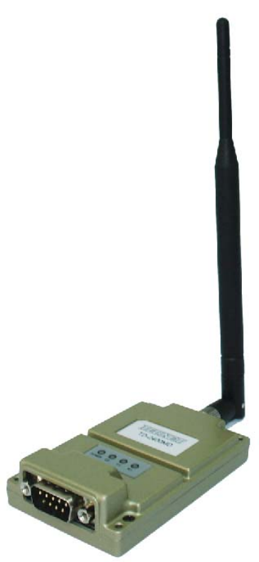
1. TD-2400MD Function
TD-2400MD is the compact size digital radio developed for supporting safety and convenience in
leisure, restaurant, superstores and public area.
No needed license because the operation is in ISM band.
Furthermore, communication range and audio quality are more improved than analogue radios.
TD-2400MD Radio’s main features are as follows;
Scalable Data Rate : 500Kbps and 1Mbps
Audio Sampling Rate : 8Kbps
PLL synthesizer type
Signal Strength Meter
Battery Status Indicator
USB PC Programming
Various Parameters and PC downloading methods
Circuit Description
TD-2400MD digital radio is consisted of RF module included MG2455, RF AMP to amplify output
power, LED Display that shows condition of drive chip and Data modem which supports RS-232C
after transforming from Digital signal into serial signal.
1. MG2455 ZigBee Chip and peripheral components
MG2455(U11) is the RF module operated in 2.4Ghz ISM band. The module is made with RF
transceiver, RF circuit, 8051 compatible MCU and several components. It follows IEEE802.15.4 and
Zigbee standard regulation. MG2455 includes zigbee stack library as zPULSE.
LM2455 data rate is from 250Kbps to 1Mbps available.
Reset circuit is consisted of Q14, R38 and C52 and operates when the voltage is below 2.5V.
Port P0.1, P0.2, P0.3is used as LED Display Port that shows TD-2400MD performance.
Port P0[5] and P0[6] are connected to EEPROM(U14) for current status restore.
P3[5], P3[6] and P3[7] are for GPIO control.
LM2455(U11)’s feature is as follows;
1) Enhanced Feature
• Scalable Data Rate : 250Kbps for ZigBee, 500Kbps and 1Mbps for private application.
• Voice Codec Support : u-law/a-law/ADPCM
• High RF RX Sensitivity of -98dBm @1.5V
• High RF TX Power of +8dBm @1.5V
• 96KB Embedded Flash Memory for Program Space.
• 8KB Data Memory
• Power Management Scheme with Deep Sleep Mode Support : under 1Ua
2) RF Transceiver
• Single-chip 2.4GHz RF Transceiver
• Low Power Consumption
• Low Operating Voltage of 1.5V
• High Sensitivity of -98dBm @1.5V
• No External T/R Switch and LPF needed
• On-chip VCO, LNA and PA
• Programmable Output Power up to +8dBm @1.5V
• Direct Sequence Spread Spectrum
• O-QPSK Modulation
• Scalable Data Rate : 250Kbps for ZigBee, 500Kbps and 1Mbps for private application.
• RSSI Measurement
• Compliant to IEEE802.15.4
3) Hardwired MAC
• Two 256byte circular FIFIs
• FIFO management
• AES-128 Engine
• CRC-16 Computation and check
•
4) I8051-Compatible Microcontroller
• Max 12x Performance of standard 8051
• 96KB Embedded Flash Memory
• 8KB Data Memory
• 128-byte CPU dedicated Memory
• 1KB Boot ROM
• Dual DPTR Support
• Multi-Bank support for 96KB program memory(3 Banks)
• 12S/PCM interface with two 128-byte FIFOs
• u-law/a-law/ADPCM voice codec
• Two high-speed UARTs with two 16byte FIFOs(up to 1Mbps)
• 4 Timers/2PWMs
• Watchdog Timer
• Sleep Timer
• Quadrature signal decoder
• 22 General purpose I/O
• Internal RC oscillator for sleep timer
• On-chip power-on-reset
• 4Channel 8-bit ADC
• SPI Master/Slave interface
• ISP (In system programming)
• Temperature Sensor
5) Clock Inputs
• 16MHz Cristal for system clock
• 19.2MHz Cristal for system clock(optional)
• 32.768KHz Cristal for sleep timer(0ptional)
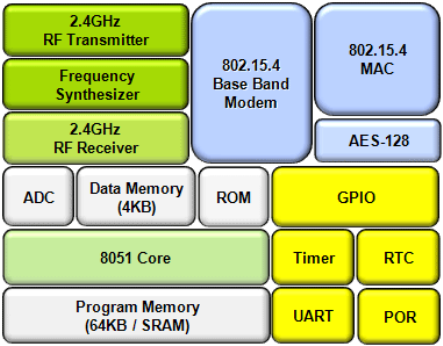
Figure 2. MG2455(U11) Block Diagram
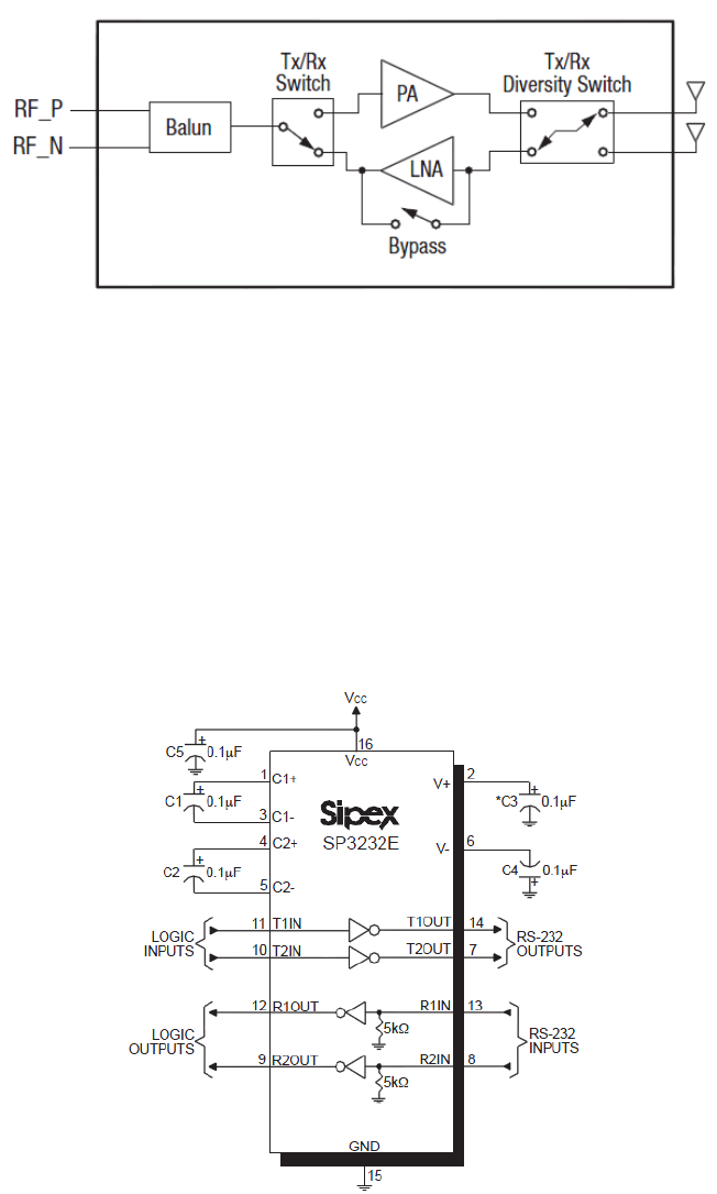
2. RF Power AMP(U13)
SKY65348(U13) is a high performance, Transmit/Receive(T/R) Front-End Module (FEM) ideally
suited for use in 2.4 GHz Industrial, Scientific, and Medical (ISM) applications.
A Double-Pole, Double-Throw (DPDT) switch allows antenna diversity and is used to select
between receive and transmit data paths.
The receive path contains a Low-Noise Amplifier (LNA) with a bypass switch. The LNA impedance
matching networks are internal to the module and have been optimized for a low Noise Figure
(NF) while maintaining good return losses into a 50 Ω source and load impedance.
The transmit path contains a Power Amplifier (PA) optimized for saturated performance.
The PA output is internally matched for optimum output power and efficiency into a 50 Ω load
impedance, and passed through an harmonic filter before passing through the DPDT switch.
The PA input provides a good return loss into a 50 Ω source impedance.
The SKY65348 has a shutdown mode to minimize power consumption. All of the eight operating
modes are controlled through three digital input pins.
When the output power is 10mW, SKY65352 is applied as RF Power AMP(U13). When 0.5W,
SKY85348 is applied as AMP. L11 and L12 take a role of matching Zigbee Chip, LM2455(U11) to
RF power AMP(U13). When the power is 500mW, the feature of SKY65348 is as follows;
• Transmit output power >±27 dBm
• Receive path NF <3.1㏈
• Analog power control
• Integrated control logic
• LNA bypass mode
• Shutdown mode
• Small footprint, MCM (28-pin, 8 x 8 mm) package (MSL3, 260 C per JEDEC J-STD-020)
• Single DC supply = 3.3V
Applications
• IEEE 802.15.4 radios
• Advanced metering infrastructure
• ISM systems
Figure 2. SKY65348(U13) Block Diagram
3. RS-232C Transceiver Chip(U15)
The SP3232E(U15) is an RS-232 transceiver solution intended for portable or handheld
applications such as notebook or palmtop computers.
The SP3232E(U15) series has a high-efficiency, charge-pump power supply that requires only
0.1μF capacitors in 3.3V operation.
This charge pump allows the SP3232E to deliver true RS-232 performance from a single power
supply ranging from +3.3V to +5.0V.
The SP3232E is 2-driver/2-receiver devices.
Figure 3. SP3232(U15) Block Diagram
4. Power Supply Circuit (U12, U16)
Power is supplied to RF Power AMP(U13) by turning input DC+5V power into DC+4V through
Regulator(U12) D-Sub connector(CON2). This is also used for input power of U16 which makes
DC+3.0V power.
Regulator(U13) turns DC+4V power into DC+3.0V to supply power to MG2455 ZigBee Chip(U11),
RS-232C Transceiver Chip(U15), EEPROM(U14) and other circuits
5. EEPROM(U14)
Saves various channel information and Parameter required in operating to TD-2400MD.
Specification
Frequency Range 24MHz
Frequency Tolerance ±5ppm
Occupied B.W 2MHz
Output Power 7\SLFDO7 dBm
VSWR 2.0 : 1
Flatness < 1㏈
Spurious Emissions
1GHz Under <-30 dBm
1GHz~2.4GHz <-30 dBm
~12GHz <-30 dBm
2ND Harmonic <-45 dBm
3rd Harmonic <-70 dBm
Inband Spurious <-45 dBm
Adjacent Channel Rejection ±3.5MHz >40 dBc
Secondary Radiated Emission <-58 dBm
Phase Noise
1MHz -110 dBc / Hz
2MHz -112 dBc / Hz
3MHz -118 dBc / Hz
RX Sensitivity <-96 dBm
Max. Input Power Level +5 dBm
Error Vector Magnitude <13%
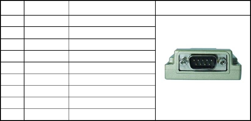
1. RS-232C 9 Pin Specification
PIN
NO Description Specification Male D-Sub Connector
1 GPIO1 TTL (DC+3.3V)
2 RX Data RS-232C
3 TX Data RS-232C
4 GPIO2 TTL (DC+3.3V)
5 Ground Ground
6 GPIO3 TTL (DC+3.3V)
7 RTS RS-232C
8 CTS RS-232C
9 DC+5.0V Input Voltage

FCC Information to User
This equipment has been tested and found to comply with the limits for a Class B digital device,
pursuant to Part 15 of the FCC Rules. These limits are designed to provide reasonable protection
against harmful interference in a residential installation. This equipment generates, uses and can
radiate radio frequency energy and, if not installed and used in accordance with the instructions, may
cause harmful interference to radio communications. However, there is no guarantee that interference
will not occur in a particular installation. If this equipment does cause harmful interference to radio or
television reception, which can be determined by turning the equipment off and on, the user is
encouraged to try to correct the interference by one of the following measures:
• Reorient or relocate the receiving antenna.
• Increase the separation between the equipment and receiver.
• Connect the equipment into an outlet on a circuit different from that to which the receiver is connected.
• Consult the dealer or an experienced radio/TV technician for help.
Caution
Modifications not expressly approved by the party responsible for compliance could void the user’s
authority to operate the equipment.
FCC Compliance Information : This device complies with Part 15 of the FCC Rules. Operation is
subject to the following two conditions:
(1) This device may not cause harmful interference, and
(2) this device must accept any interference received, including interference that may cause undesired operation
IMPORTANT NOTE:
FCC RF Radiation Exposure Statement:
This equipment complies with FCC RF radiation exposure limits set forth for an uncontrolled
environment. This equipment should be installed and operated with a minimum distance of 20
centimeters between the radiator and your body.This transmitter must not be co-located or operating
in conjunction with any other antenna or transmitter.
This device is intended only for OEM integrators under the following conditions:
1) The antenna must be installed such that 20 cm is maintained between the antenna and users, and
2) The transmitter module may not be co-located with any other transmitter or antenna,
3) OEM shall not supply any tool or info to the end-user regarding to Regulatory Domain change.
As long as 3 conditions above are met, further transmitter test will not be required. However, the OEM
integrator is still responsible for testing their end-product for any additional compliance requirements
required with this module installed (for example, digital device emissions, PC peripheral requirements,
etc.).
IMPORTANT NOTE: In the event that these conditions can not be met (for example certain laptop
configurations or co-location with another transmitter), then the FCC authorization is no longer
considered valid and the FCC ID can not be used on the final product. In these circumstances, the
OEM integrator will be responsible for re-evaluating the end product (including the transmitter) and
obtaining a separate FCC authorization.
Maximum antenna gain allowed for use with this device is dBi
End Product Labeling
This transmitter module is authorized only for use in device where the antenna may be installed such
that 20 cm may be maintained between the antenna and users. The final end product must be labeled
in a visible area with the following: “Contains FCC ID: 9627'0'”
Manual Information To the End User
The OEM integrator has to be aware not to provide information to the end user regarding how to
install or remove this RF module in the user’s manual of the end product which integrates this module.
The end user manual shall include all required regulatory information/warning as show in this manual.
GUIDANCE REQUIREMENT / RESPONSIBILITY: Pursuant to the Transmitter
Module Equipment Authorization Guide (KDB 996369 D01), the party responsible for the
module grant shall provide guidance to the host manufacturer for compliance with the Part
15B requirements. Please acknowledge and document this responsibility.