Yale Electronics B922BL Bluetooth Sport Headset User Manual
Shenzhen Yale Electronics Co., Ltd. Bluetooth Sport Headset
UserManual.wiki
>
Yale Electronics
>
B922BL User Manual
User Manual
Navigation menu
Upload a User Manual
Namespaces
Wiki Guide
HTML
PDF
Info
Views
User Manual
Discussion / Help
Navigation

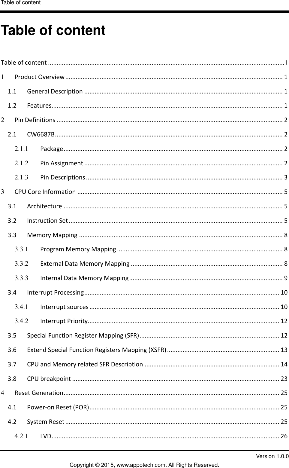
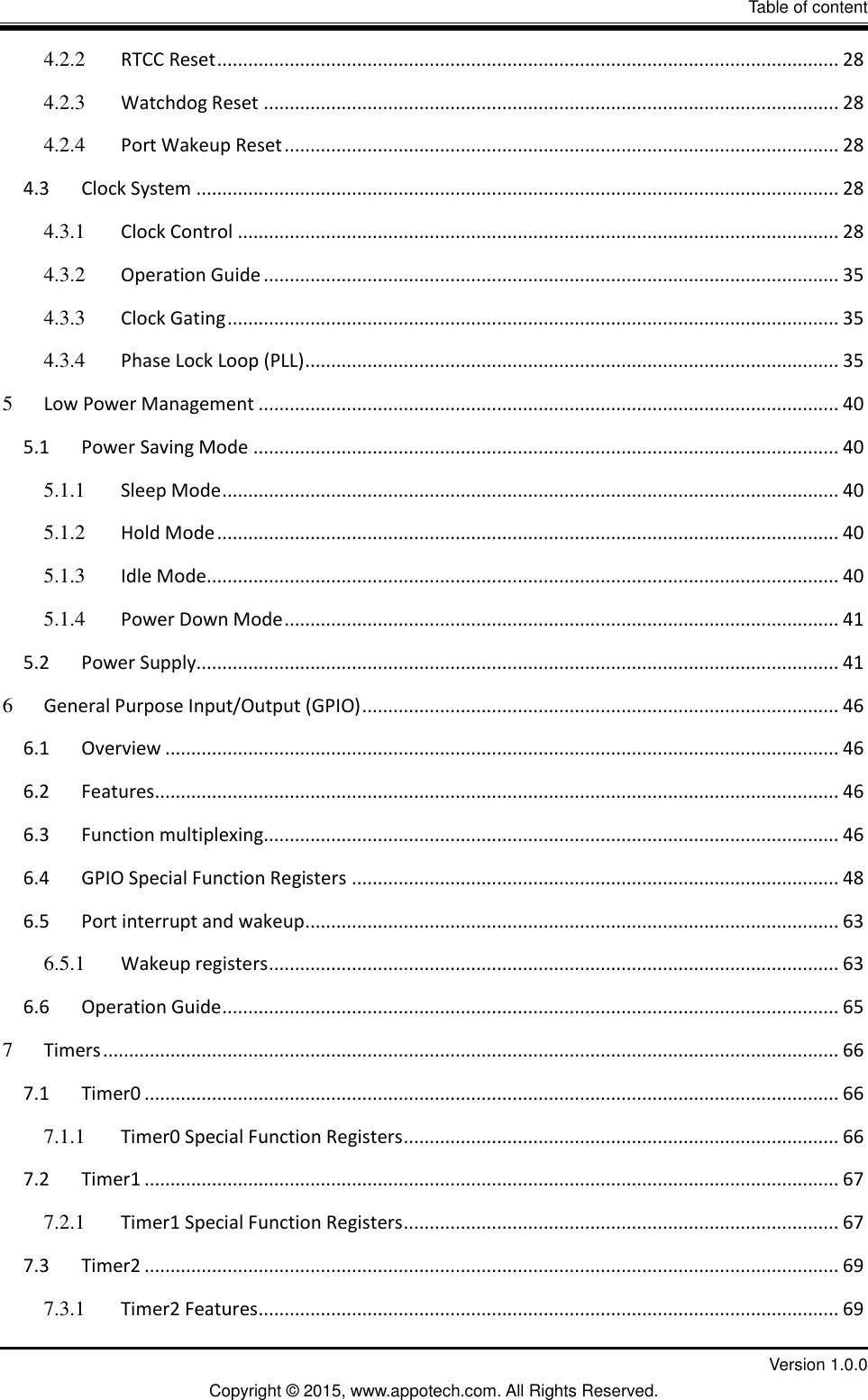
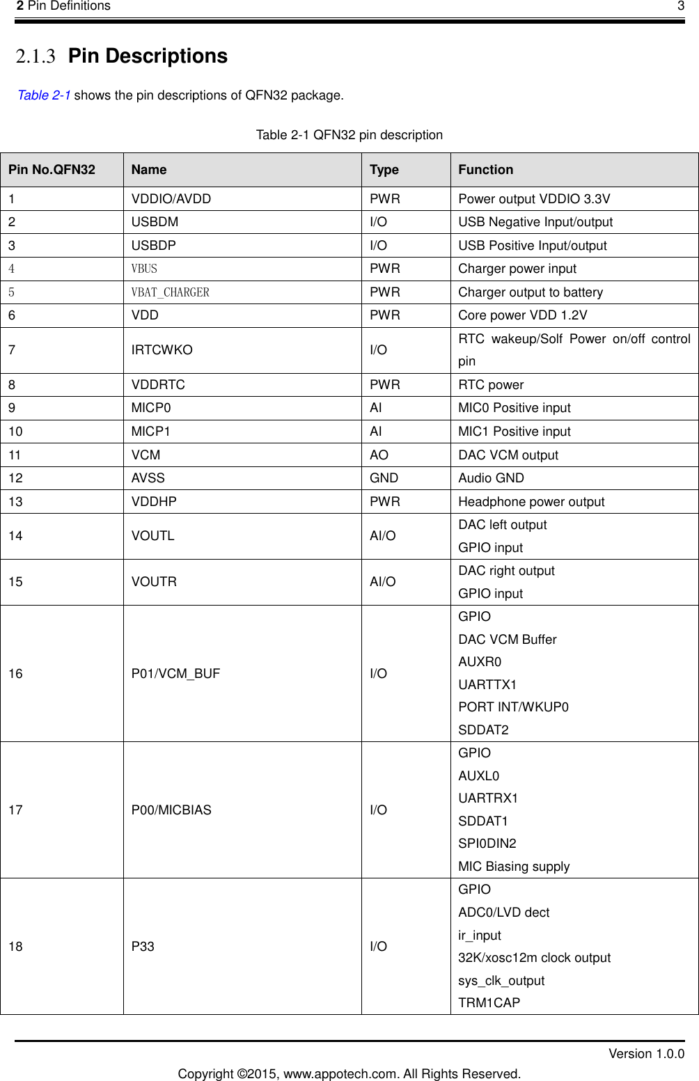
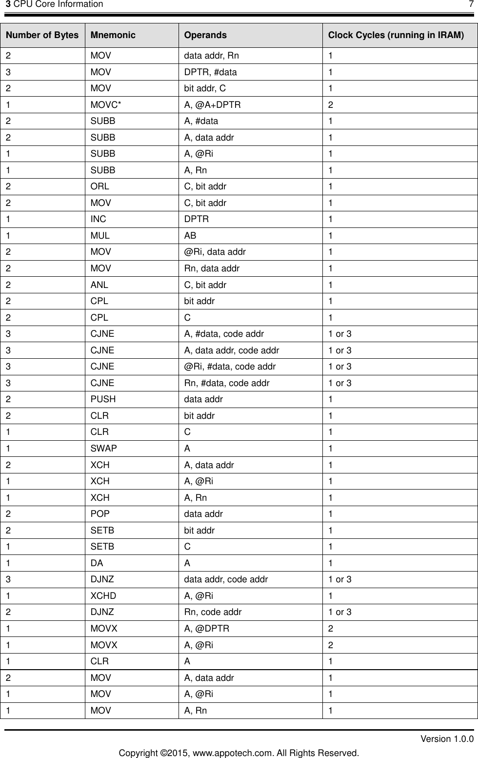
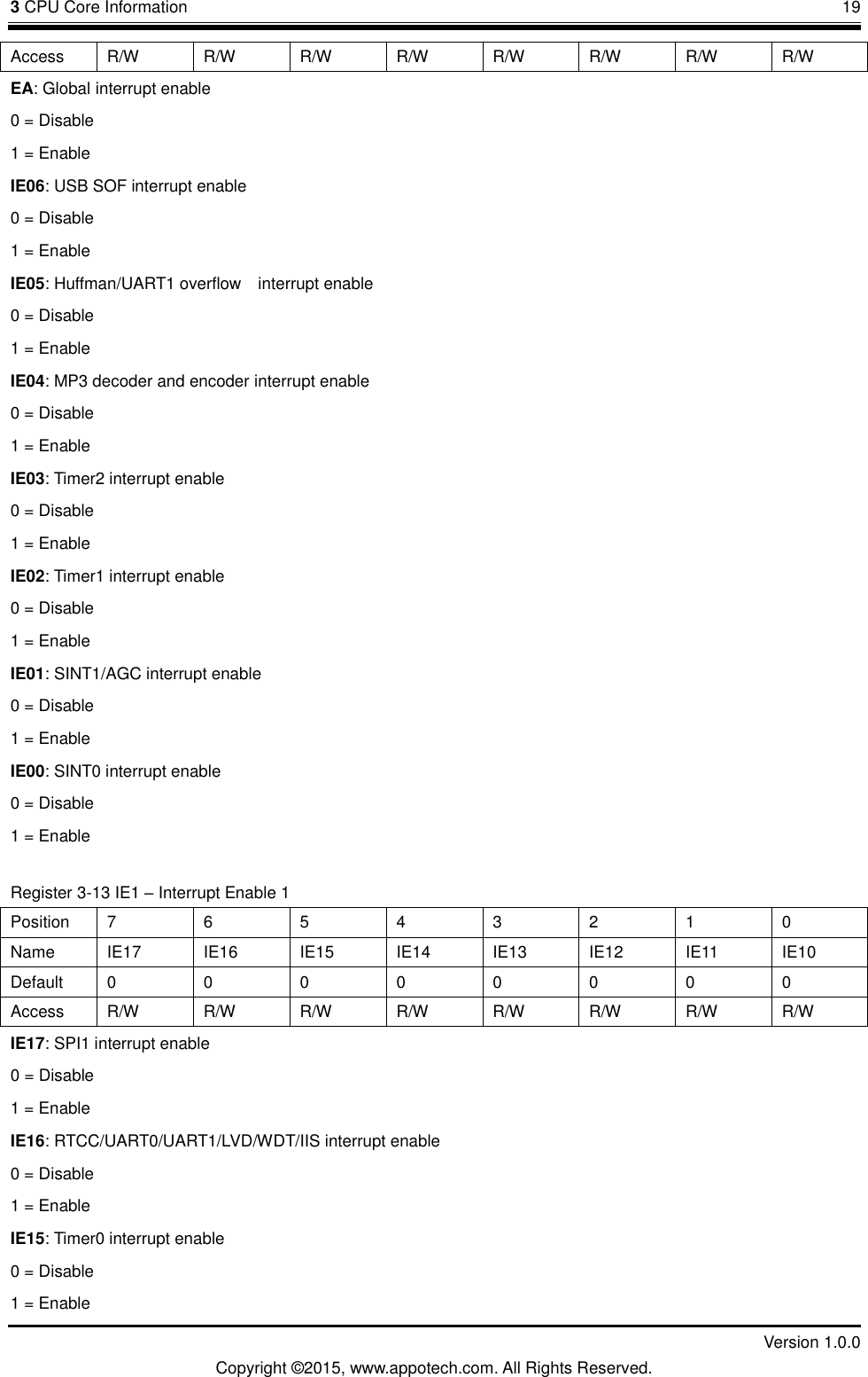
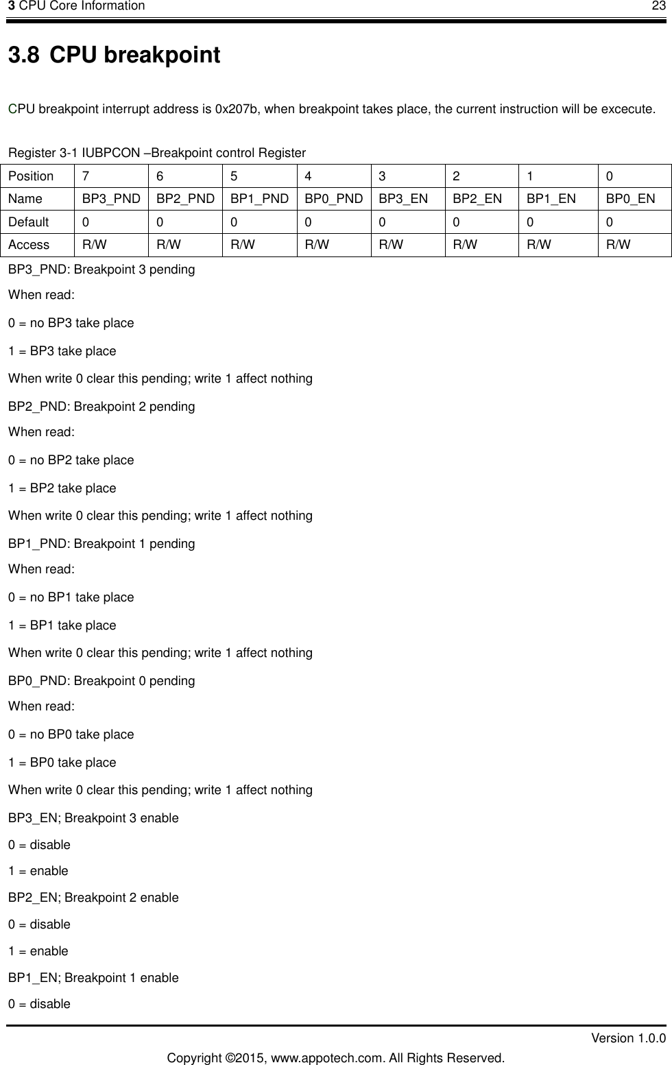
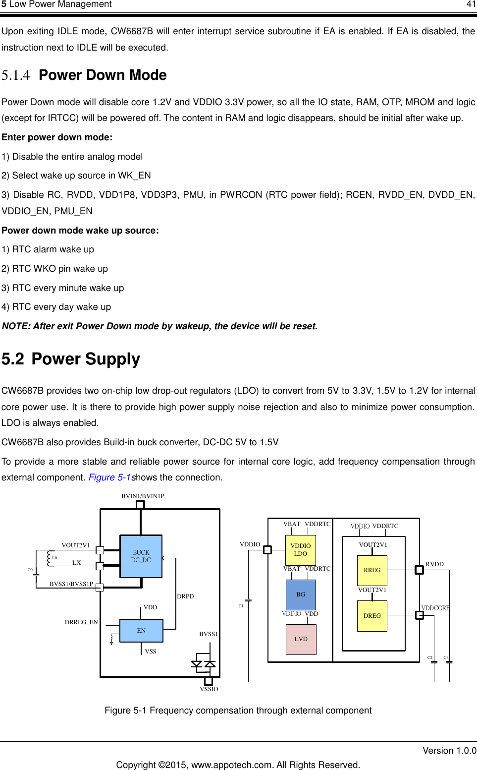
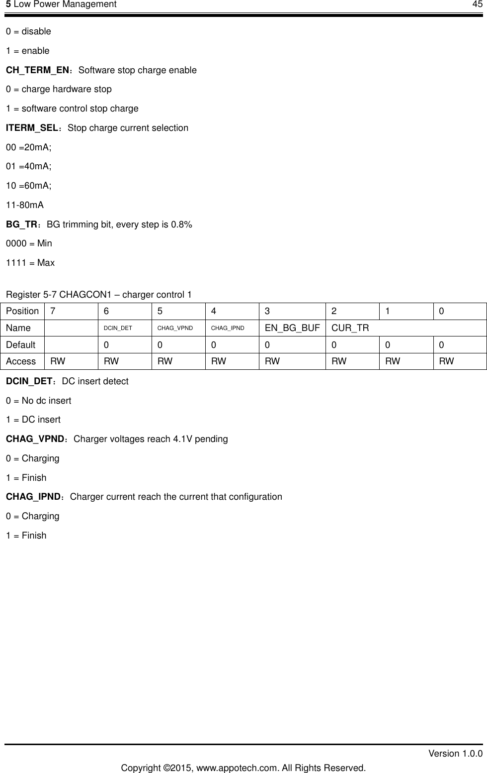
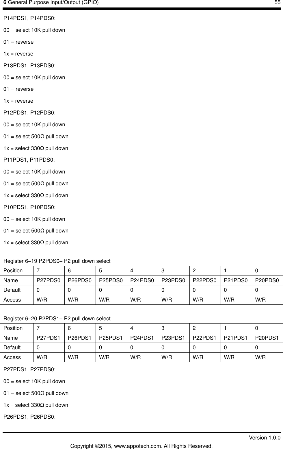
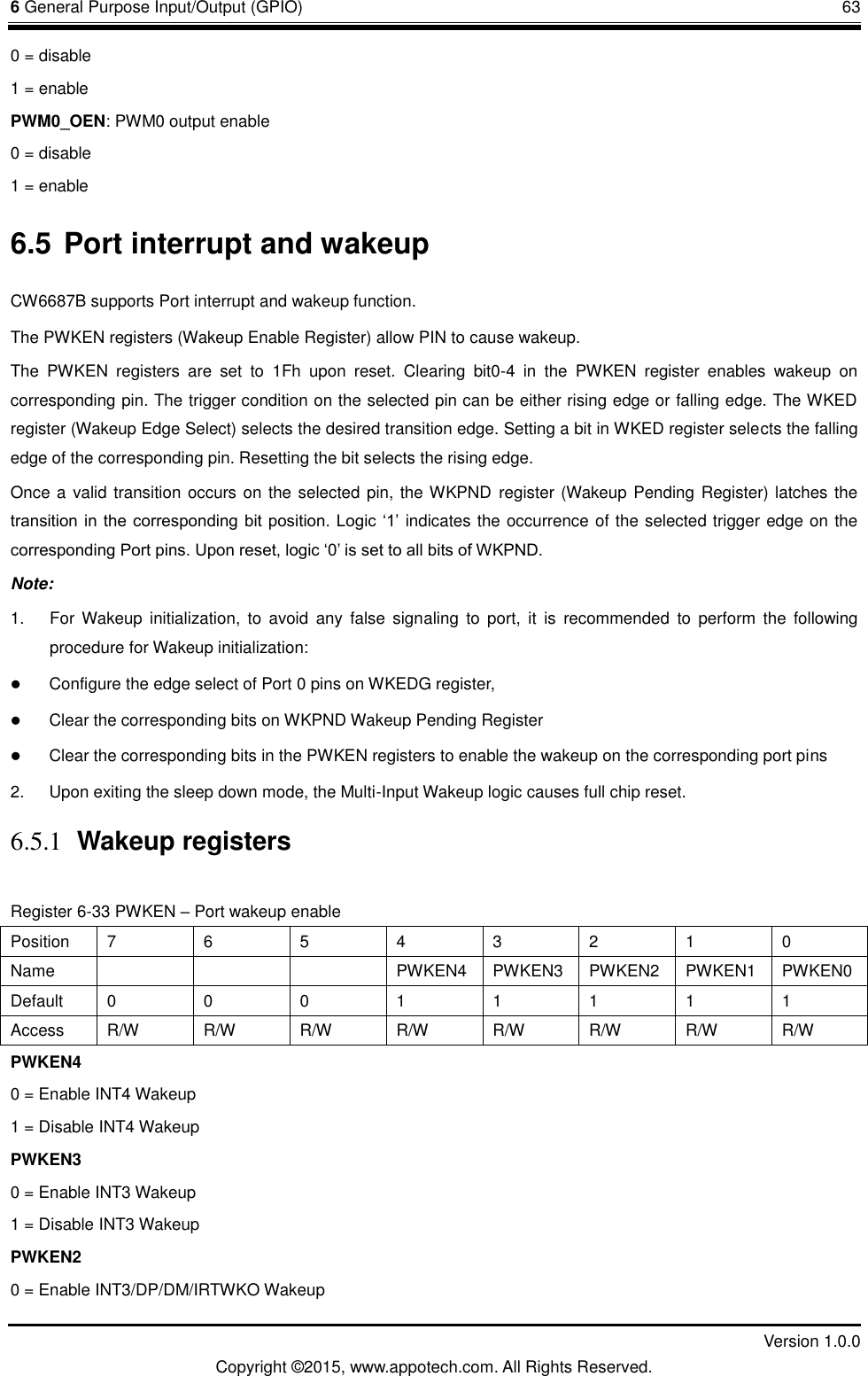
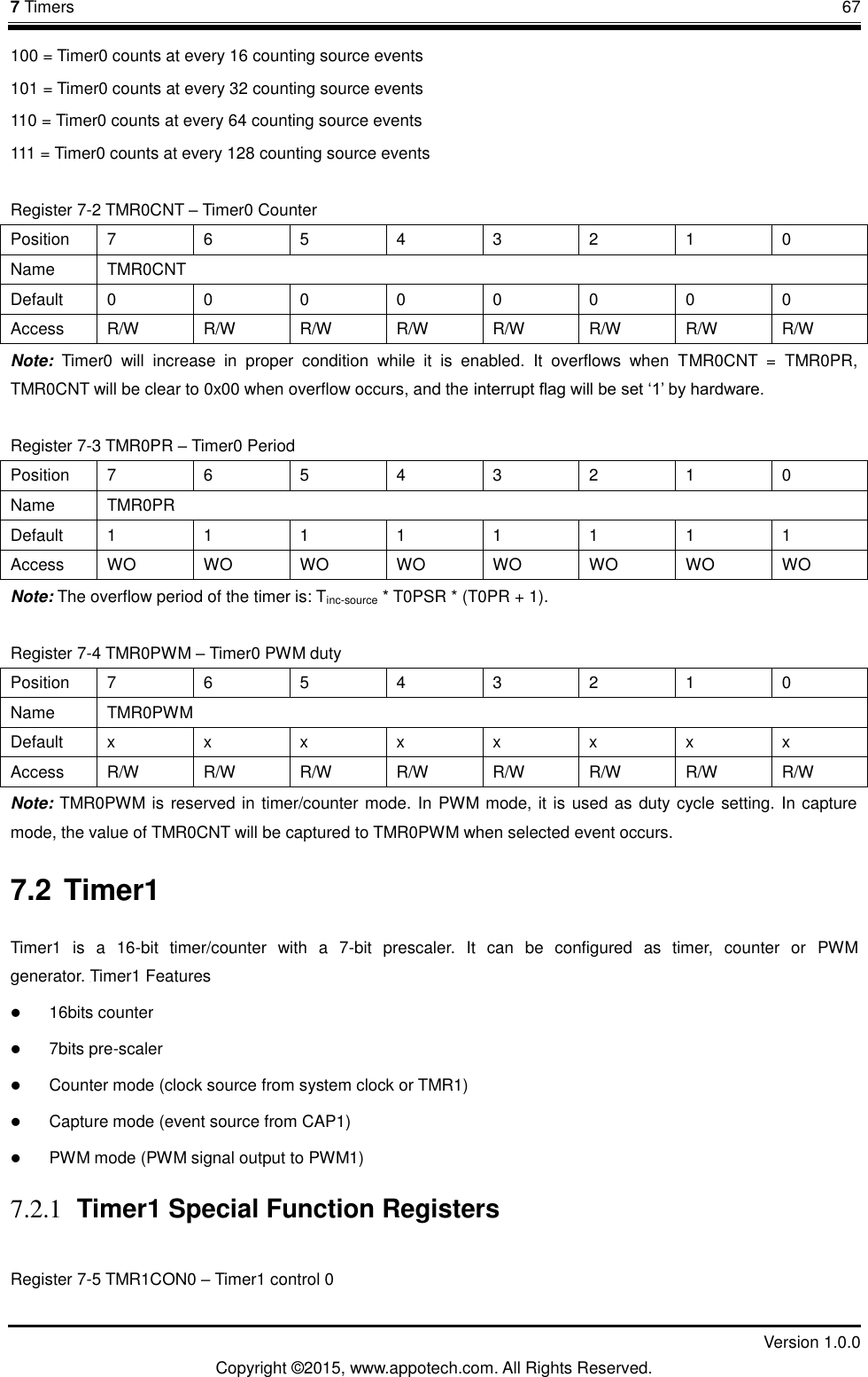
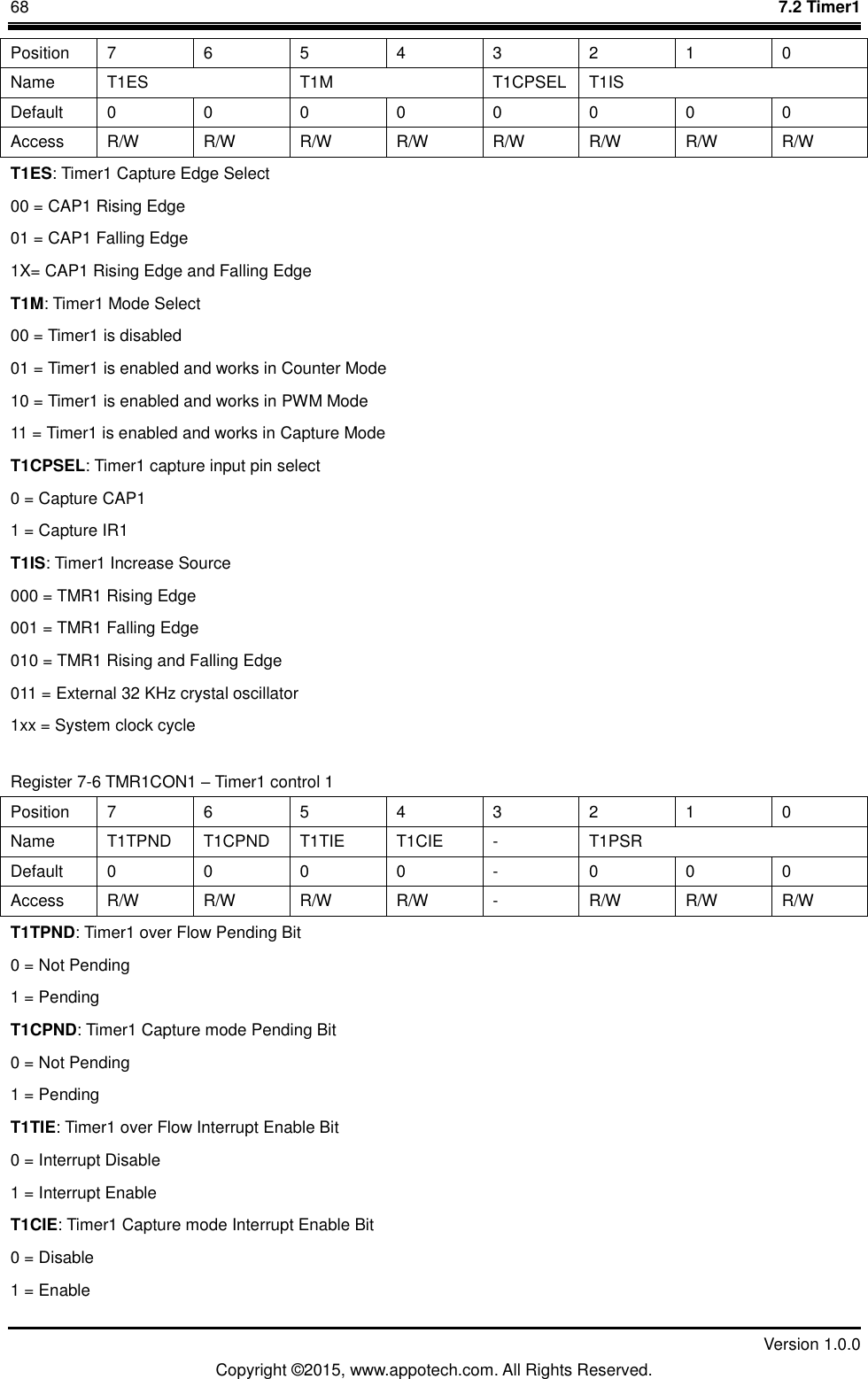
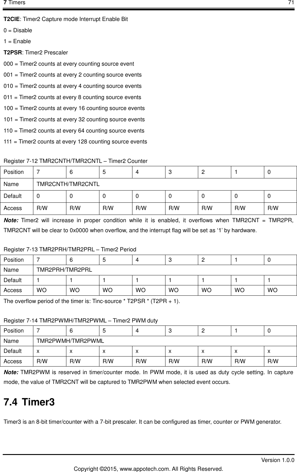
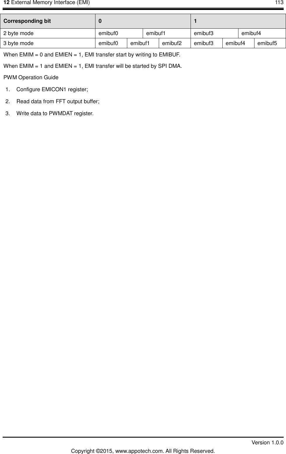
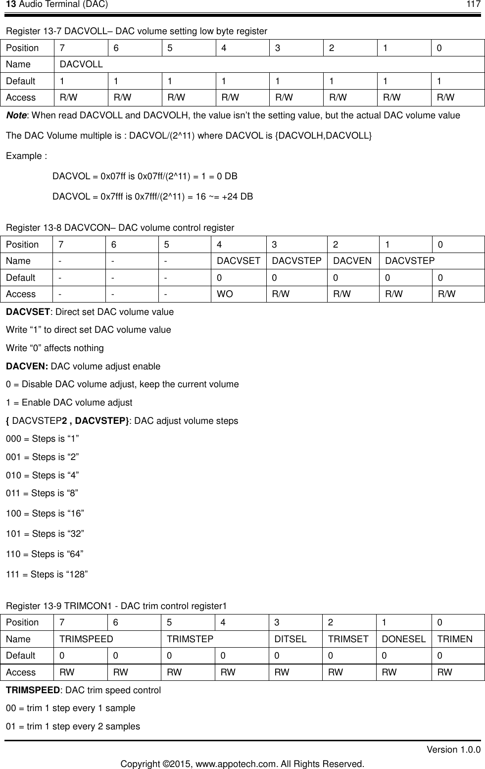
![10 3.4 Interrupt Processing Version 1.0.0 Copyright ©2015, www.appotech.com. All Rights Reserved. Indirect addressing onlyDirect and Indirect addressingDirect addressing00H7FH80HFFHUpper128Lower128SFRFFH80H Figure 3-3 Internal data memory mapping As shown in Figure 3-4 the Lowest 32 bytes in Lower 128 are grouped into 4 banks of 8 registers. Program instructions call out these registers as R0 through R7. Two bits in the PSW select which register bank are in use. 00H 07H08H 0FH10H 1FH18H 1FH20H2FH7FH00011011BANK SELECT BITS IN PSWReset value of SPBit addressable space Figure 3-4 Lowest 32 bytes in Internal data memory Lower 128 3.4 Interrupt Processing 3.4.1 Interrupt sources The CW6687B provides 15 interrupt sources. All interrupts are controlled by a series combination of individual enable bits and a global enable (EA) in the interrupt-enable register (IE0.7). Setting EA to logic 1 allows individual interrupts to be enabled. Setting EA to logic 0 disables all interrupts regardless of the individual interrupt-enable settings. The interrupt enables and priorities are functionally identical to those of the 80C52. The CW6687B provides 3 sets of vectors entry addresses, starting from 0x0003, 0x4003 and 0x8003. The vector base address is set by DPCON [7:6]. Table 3-2 lists the interrupt summary. Table 3-2 Interrupt Summary](https://usermanual.wiki/Yale-Electronics/B922BL/User-Guide-3812035-Page-18.png)
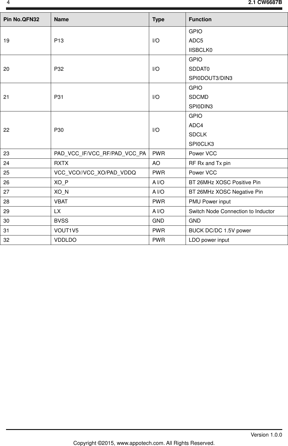
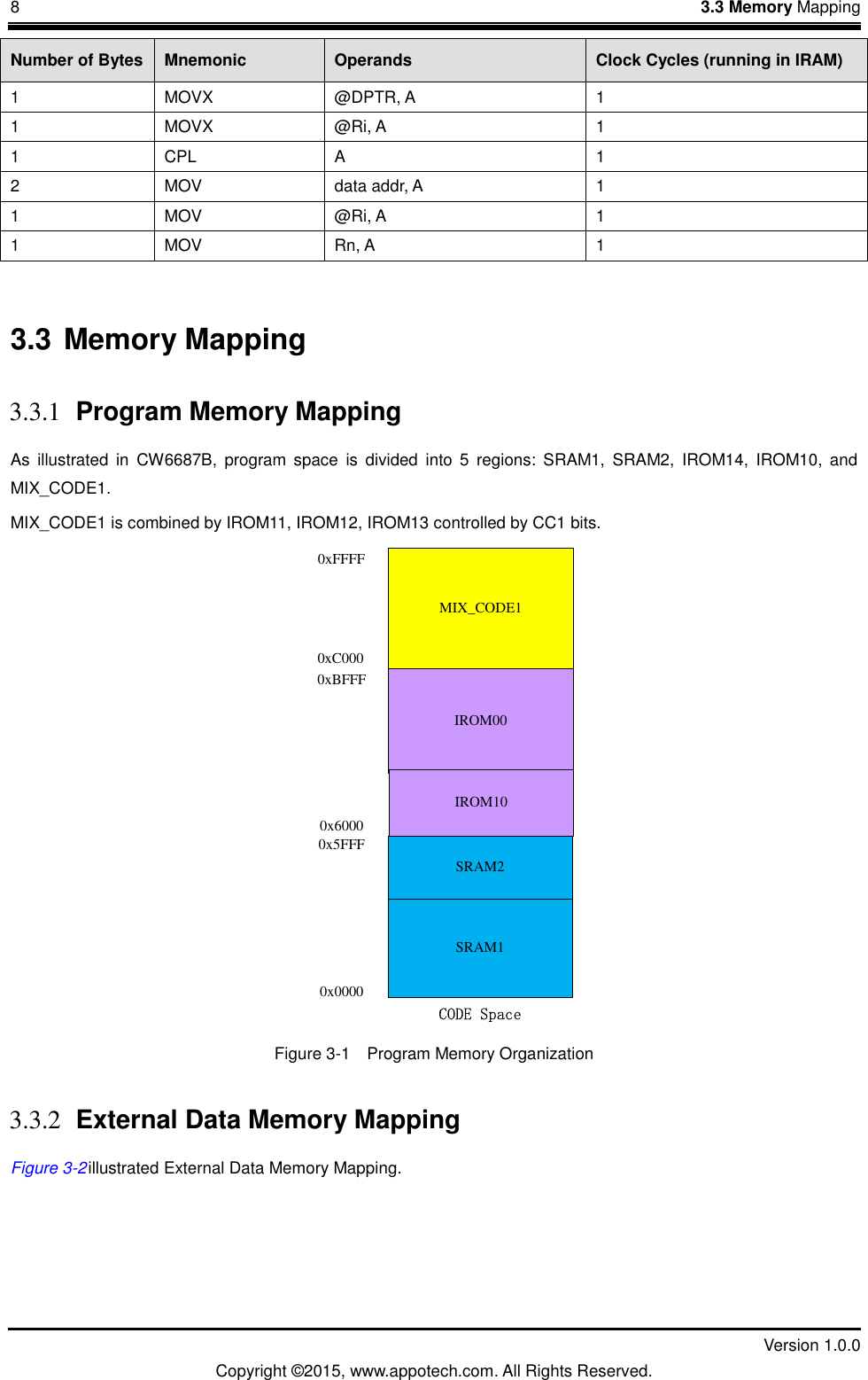
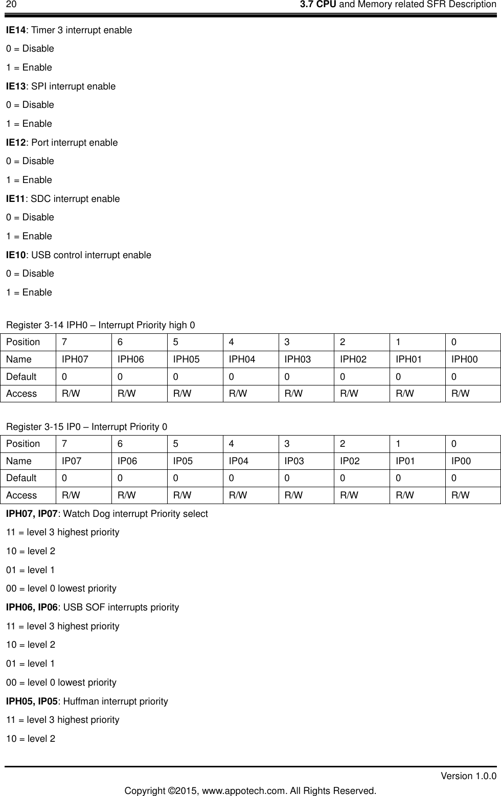
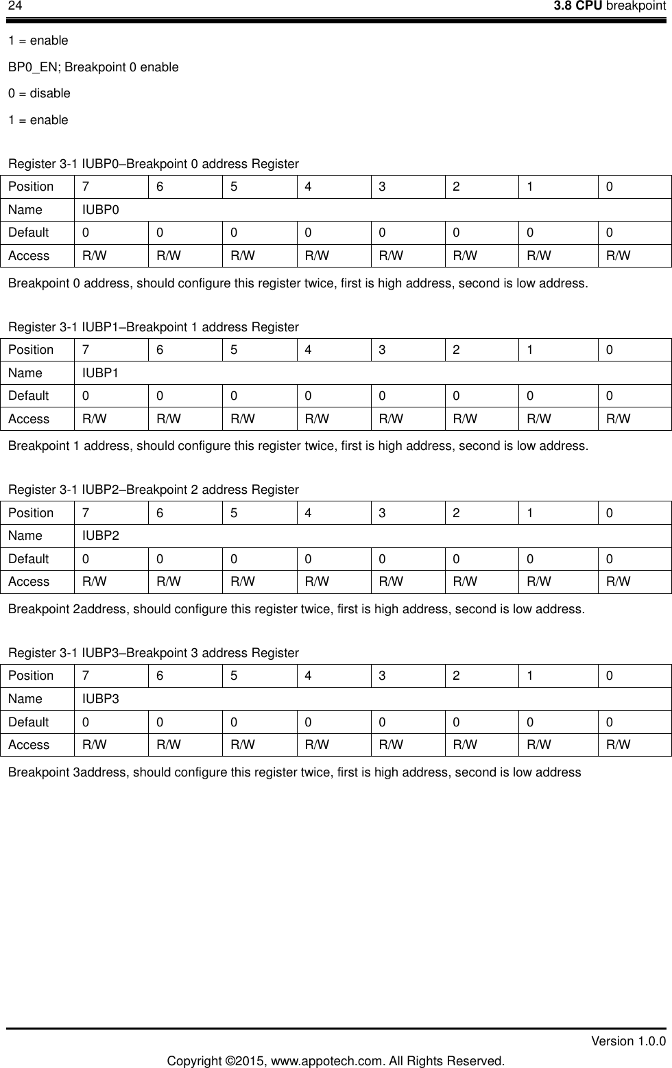
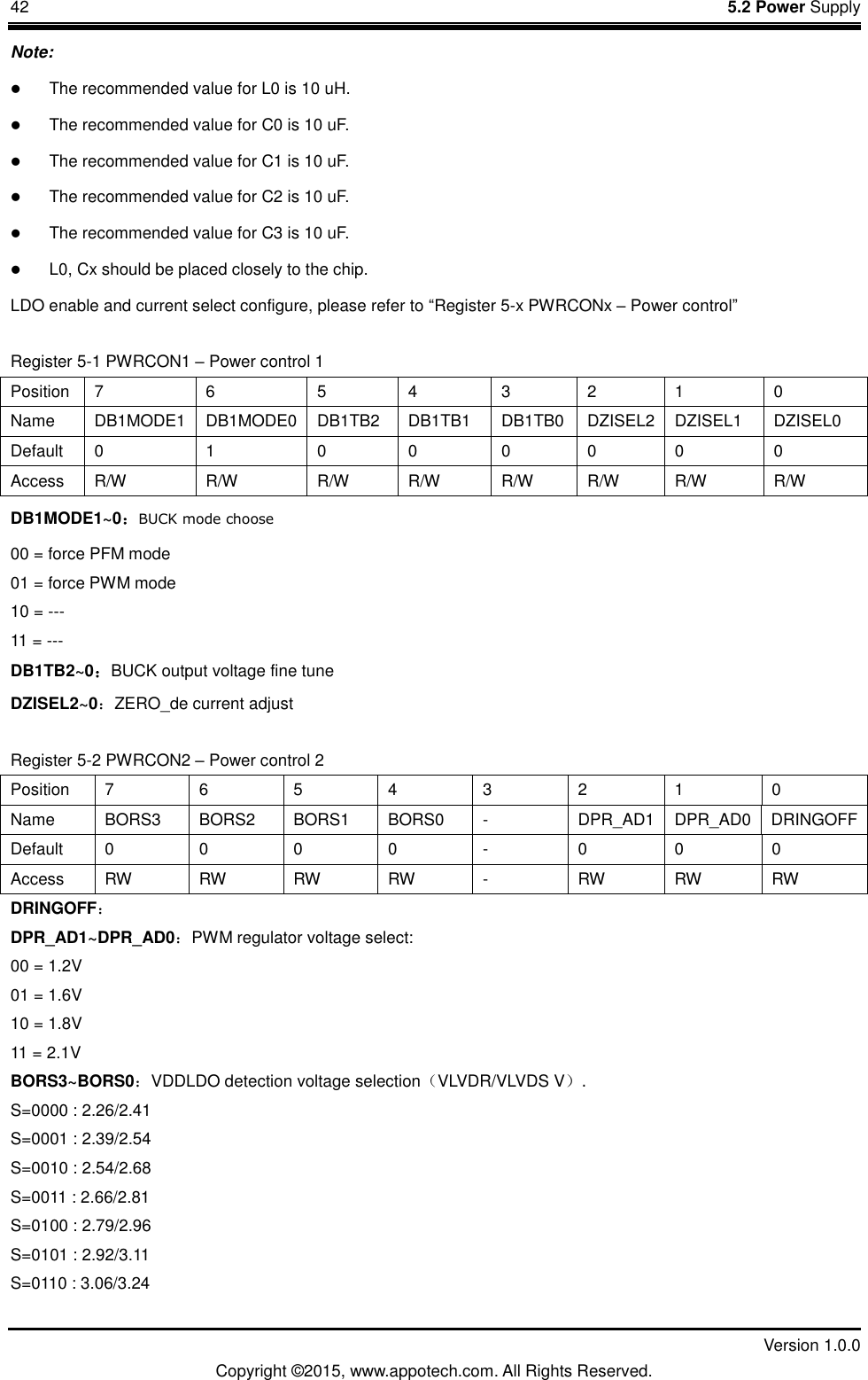
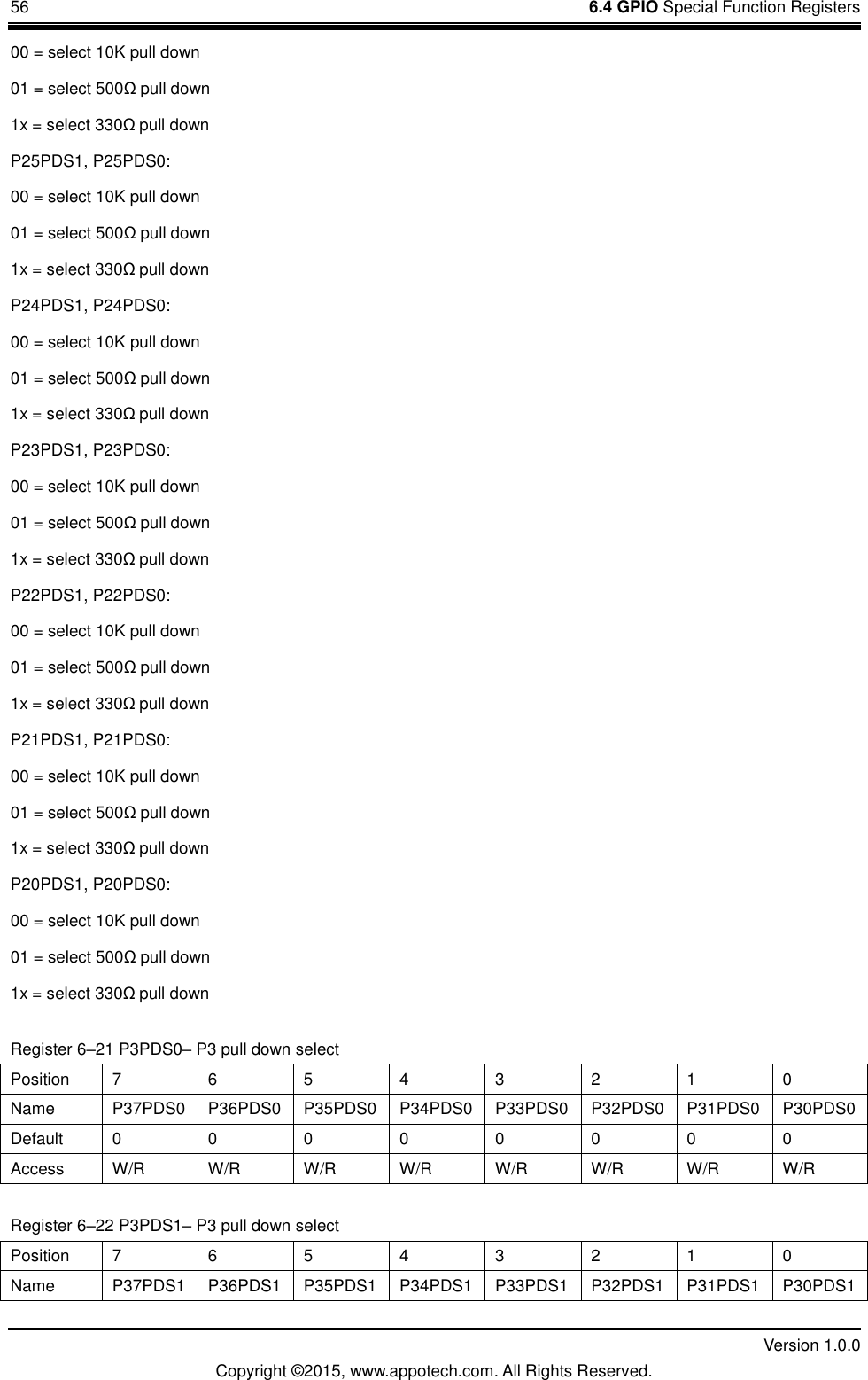
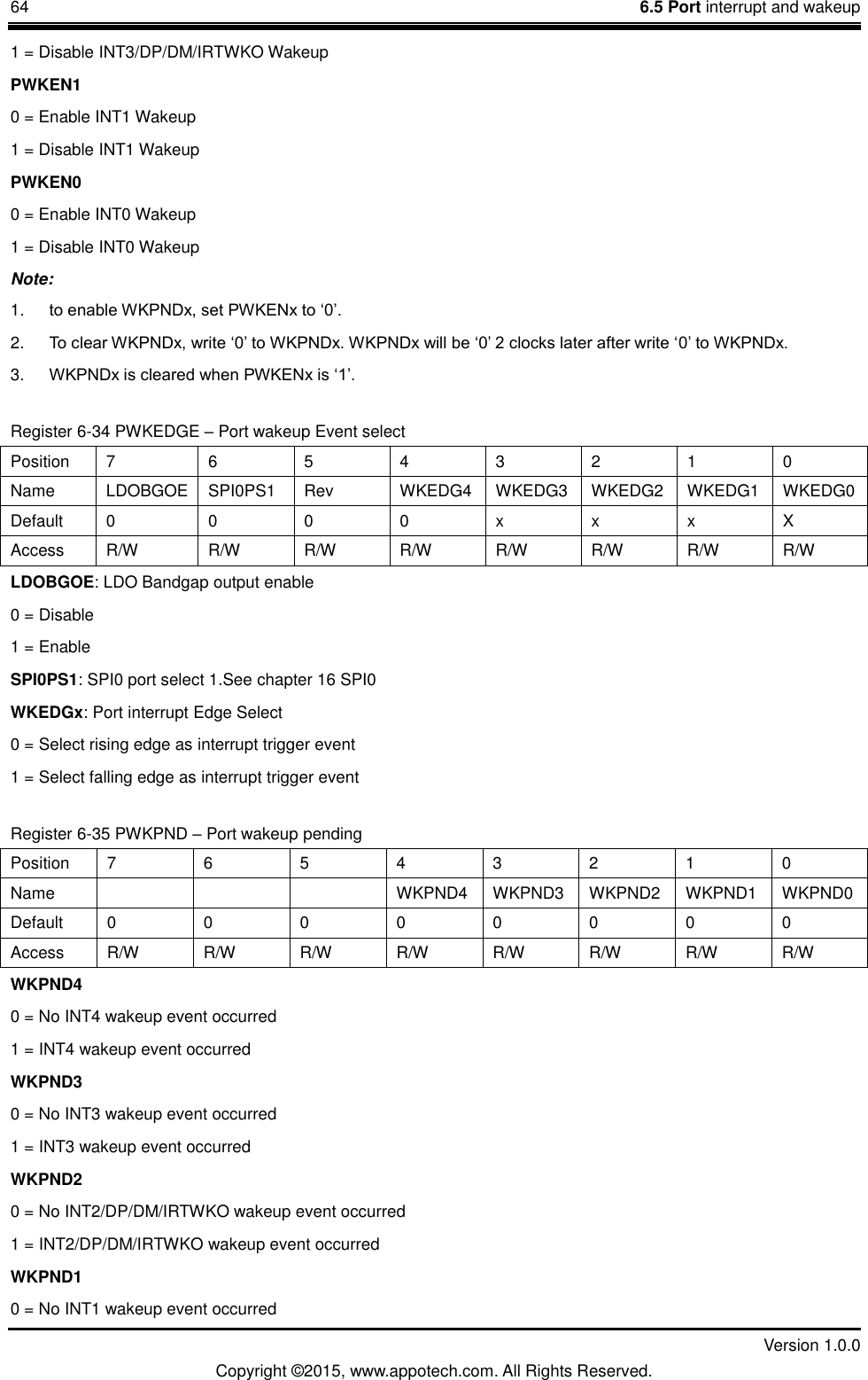
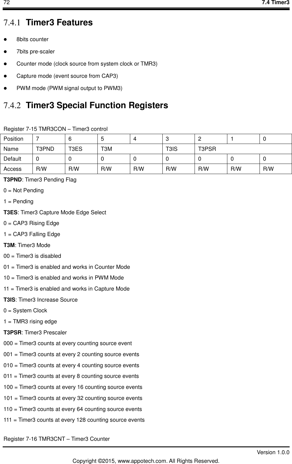
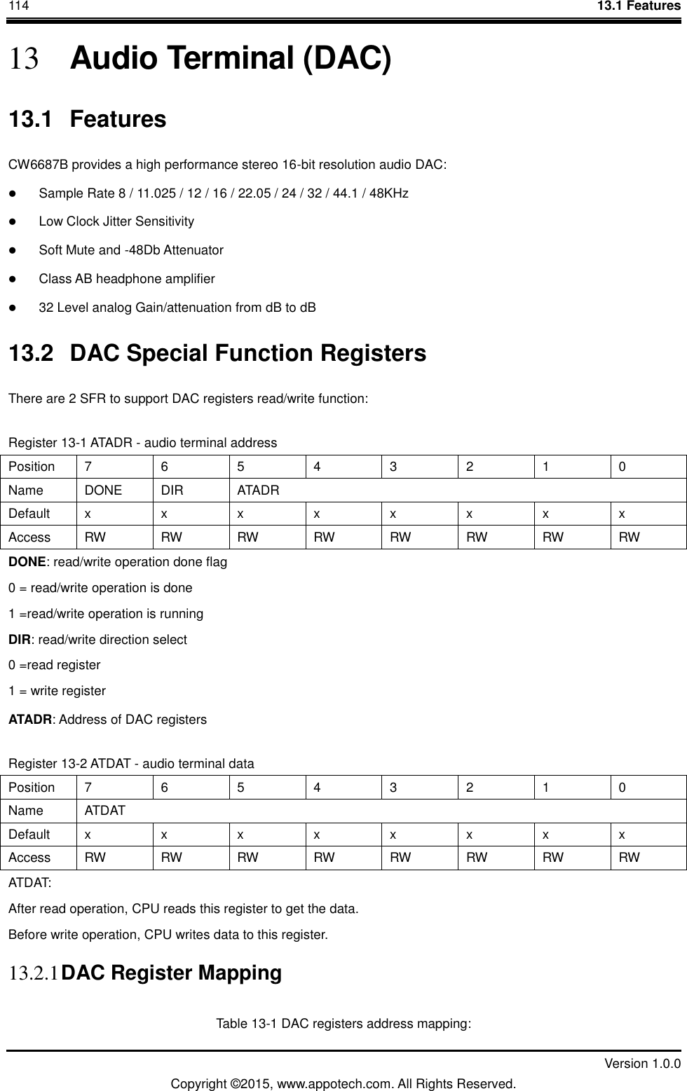
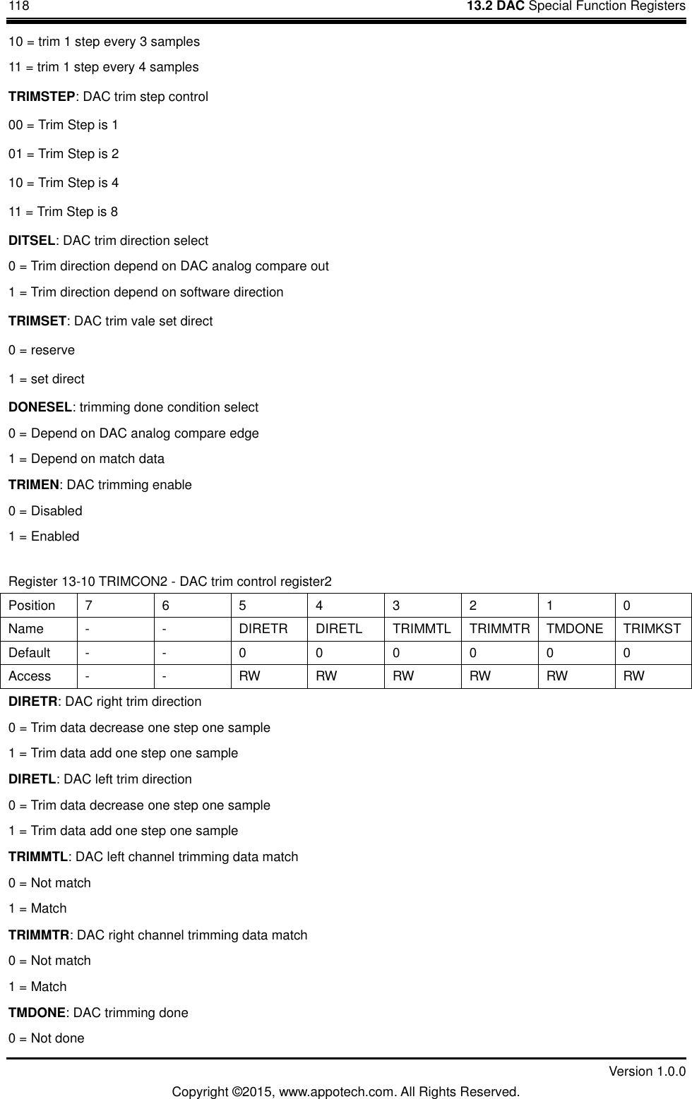
![3 CPU Core Information 11 Version 1.0.0 Copyright ©2015, www.appotech.com. All Rights Reserved. Interrupt Sources Interrupt Vector Interrupt Number Natural Order Interrupt Flag Interrupt Enable Bit Priority Control Bit SINT0 0x0003 0x4003 0x8003 0 1 SPMODE.7 IE0.0 IPH0.0 IP0.0 SINT1 AGC 0x000B 0x400B 0x800B 1 2 SPMODE.6 AGCDMACON.0 IE0.1 IPH0.1 IP0.1 Timer 1 0x0013 0x4013 0x8013 2 3 TMR1CON.7 TMR1CON.6 IE0.2 IPH0.2 IP0.2 Timer 2 0x001B 0x401B 0x801B 3 4 TMR2CON.7 TMR2CON.6 IE0.3 IPH0.3 IP0.3 MP3/FFT1 0x0023 0x4023 0x8023 4 5 AUCON7.6 AUCON7.5 AUCON7.4 AUCON7.3 AUCON7.2 AUCON7.1 AUCON7.0 AUCON11.6 FFT1CON1.1 IE0.4 IPH0.4 IP0.4 Huffman/ UART1 (overflow) 0x002B 0x402B 0x802B 5 6 HFMCON.7 HFMCON.6 UART1STA.1 IE0.5 IPH0.5 IP0.5 USBSOF UART1 BTRAM 0x0033 0x4033 0x8033 6 7 USBCON2.1 UART1STA.3&UART1STA2 BTRAM_CON0[6]& BTRAM_CON1[4] IE0.6 IPH0.6 IP0.6 USBCTL 0x003B 0x403B 0x803B 7 8 IE1.0 IPH1.0 IP1.0 SDC 0x0043 0x4043 0x8043 8 9 SDCON1.5 SDCON1.4 IE1.1 IPH1.1 IP1.1 PORT 0x004B 0x404B 0x804B 9 10 WKPND IE1.2 IPH1.2 IP1.2 SPI0 0x0053 0x4053 0x8053 10 11 SPI0CON.7 IE1.3 IPH1.3 IP1.3 Timer 3 0x005B 11 12 TMR3CON.7 IE1.4 IPH1.4](https://usermanual.wiki/Yale-Electronics/B922BL/User-Guide-3812035-Page-19.png)
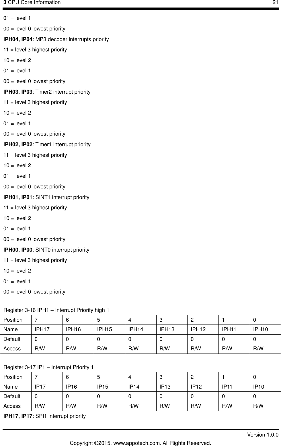
![14 3.7 CPU and Memory related SFR Description Version 1.0.0 Copyright ©2015, www.appotech.com. All Rights Reserved. 7808H IRTADT3 IRDAT2 IRDAT1 IRDAT0 IIS_VALBIT SPMODE1 PIE1 PWRCON2 7800H PWRCON1 RC_TRIM IIS_ADR1 RC_TEST SDDPTR SDDCNT SDCPTR SDBAUD 3.7 CPU and Memory related SFR Description Register 3-1 DPCON – Data Pointer Configure Register Position 7 6 5 4 3 2 1 0 Name IA DPID0 DPID1 DPAID DPTSL EINSTEN DPSEL Default 1 0 0 0 0 0 0 0 Access R/W R/W R/W R/W R/W R/W R/W R/W IA: Select Interrupt Vector‟s Base Address 00 = Base address is 0x0003 01 = Base address is 0x4003 10 = Base address is 0x8003 11 = Base address is 0xc003 note:interrupt address is determined by SPMODE1[4] 0 = interrupt base address depend on IA 1 = interrupt base address is 0x2000 DPID0: DPTR0 increase direction control 0 = DPTR increase 1 = DPTR decrease DPID1: DPTR1 increase direction control 0 = DPTR increase 1 = DPTR decrease DPAID: DPTR auto increment enables 0 = Auto increment disable 1 = Auto increment enable DPTSL: DPSEL toggle enable 0 = DPSEL toggle disable 1 = DPSEL toggle enable EINSTEN: Extern instruction enables 0 = Disable 1 = Enable DPSEL: DPTR Select 0 = Active DPTR0 1 = Active DPTR1 Data Pointer Register is a 16-bit address pointer,it can split up into two registers,DPL and DPH. Data pointer register is always used as indirect addressing register. Note:Interrupt address is determined by SPMODE1[4]](https://usermanual.wiki/Yale-Electronics/B922BL/User-Guide-3812035-Page-22.png)
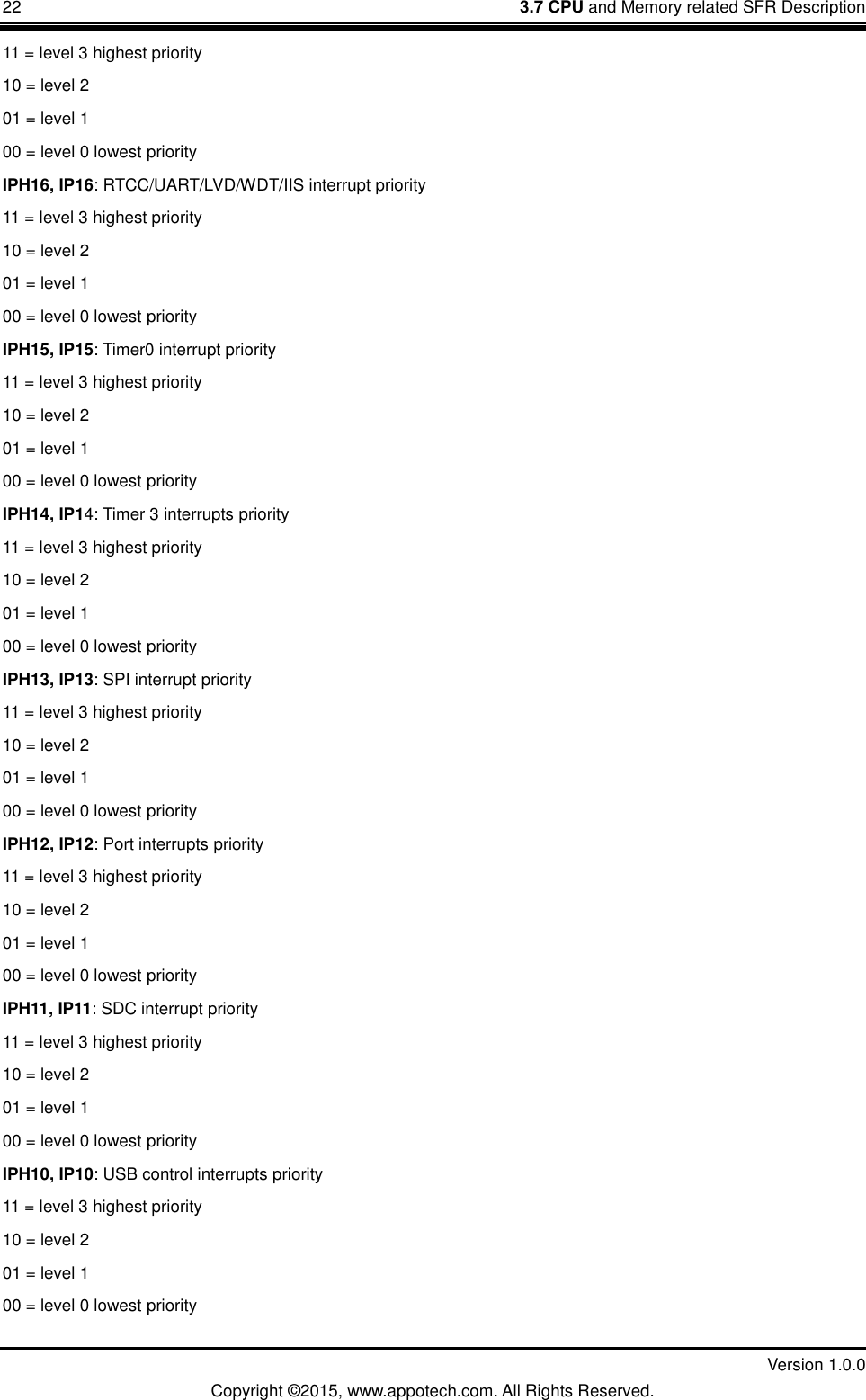
![18 3.7 CPU and Memory related SFR Description Version 1.0.0 Copyright ©2015, www.appotech.com. All Rights Reserved. 0 = disable 1 = enable SPI1_MAP: SPI1 port mapping 0 = Select P04, P05, P06 1 = Select P30, P31, P32 INTADR_SEL: interrupt address select 0 = depend on DPCON IA 1 = 0x2000 PAPAMODE: papa mode 0 = normal mode 1 = Parallel mode SPIINITMODE: SPI Flash initial mode 0 = normal mode 1 = SPI initial mode SBCDEC_MEN: SBC decoder module enables 0 = Disable 1 = Enable MP3DEC_MEN: MP3 decoder module enables 0 = Disable 1 = Enable Note: SPMODE1[1:0] register can be written to “0”, but can‟t be written to “1” after writing “0”. Register 3-11 MEMCON – Memory Mapping Configure Position 7 6 5 4 3 2 1 0 Name CC1 CC0 Default 0 0 0 0 0 0 0 0 Access WO WO RO R/W R/W R/W R/W R/W CC1: MIX_CODE3 mapping 000 = IROM01 map to address 0xc000~0xffff 001 = IROM02 map to address 0xc000~0xffff 010 = IROM03 map to address 0xc000~0xffff 011 = IROM11 map to address 0xc000~0xffff 100 = IROM12 map to address 0xc000~0xffff 101 = SRAM3/SRAM2 map to address 0xc000~0xffff Register 3-12 IE0 – Interrupt Enable 0 Position 7 6 5 4 3 2 1 0 Name EA IE06 IE05 IE04 IE03 IE02 IE01 IE00 Default 0 0 0 0 0 0 0 0](https://usermanual.wiki/Yale-Electronics/B922BL/User-Guide-3812035-Page-26.png)
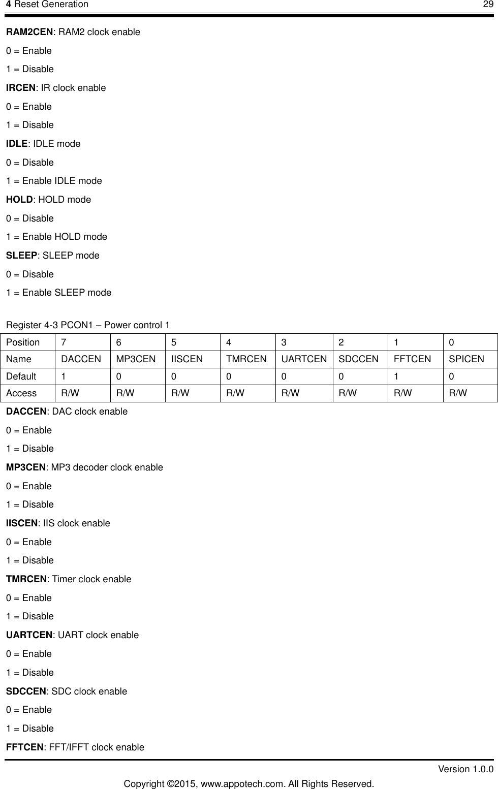
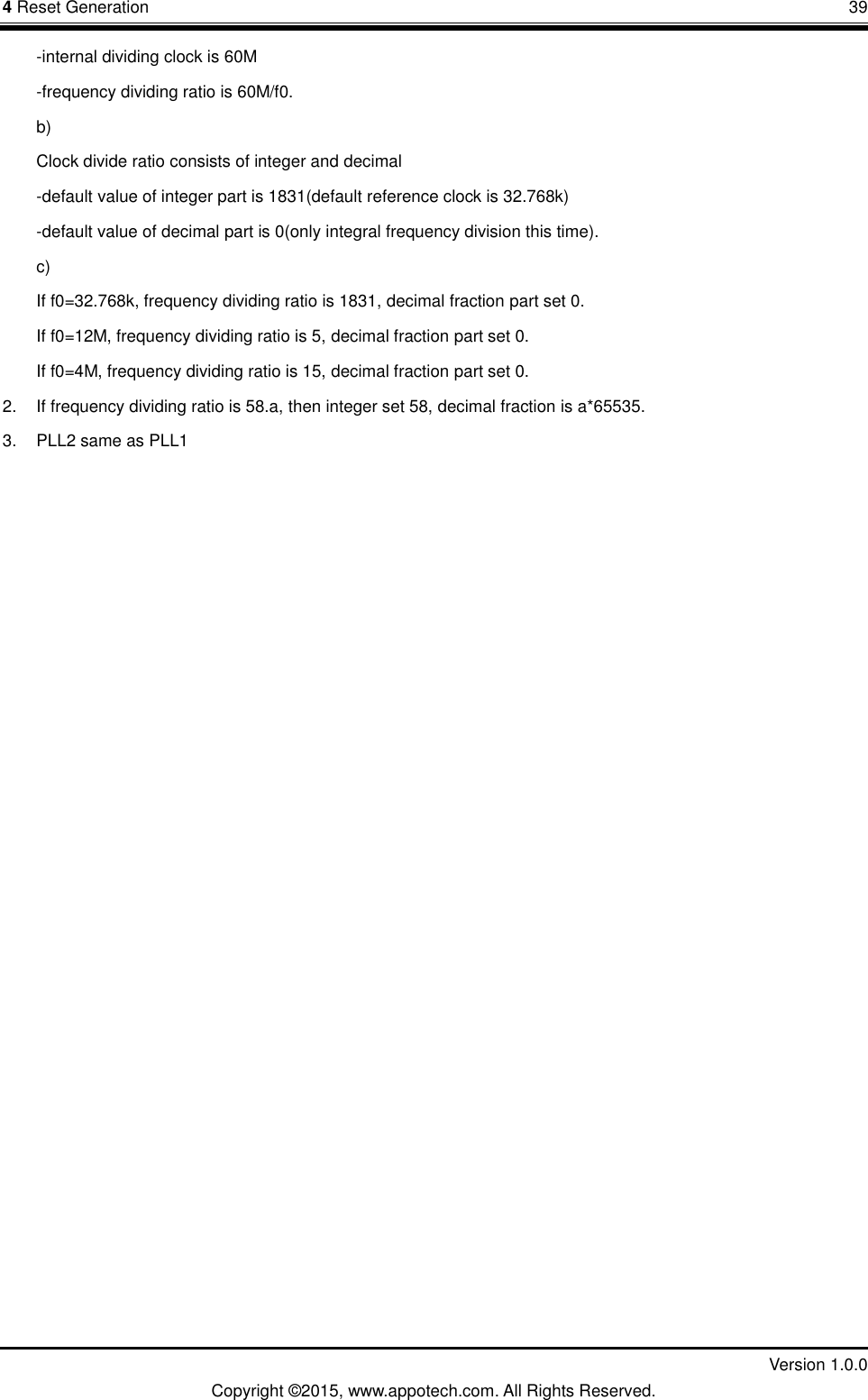
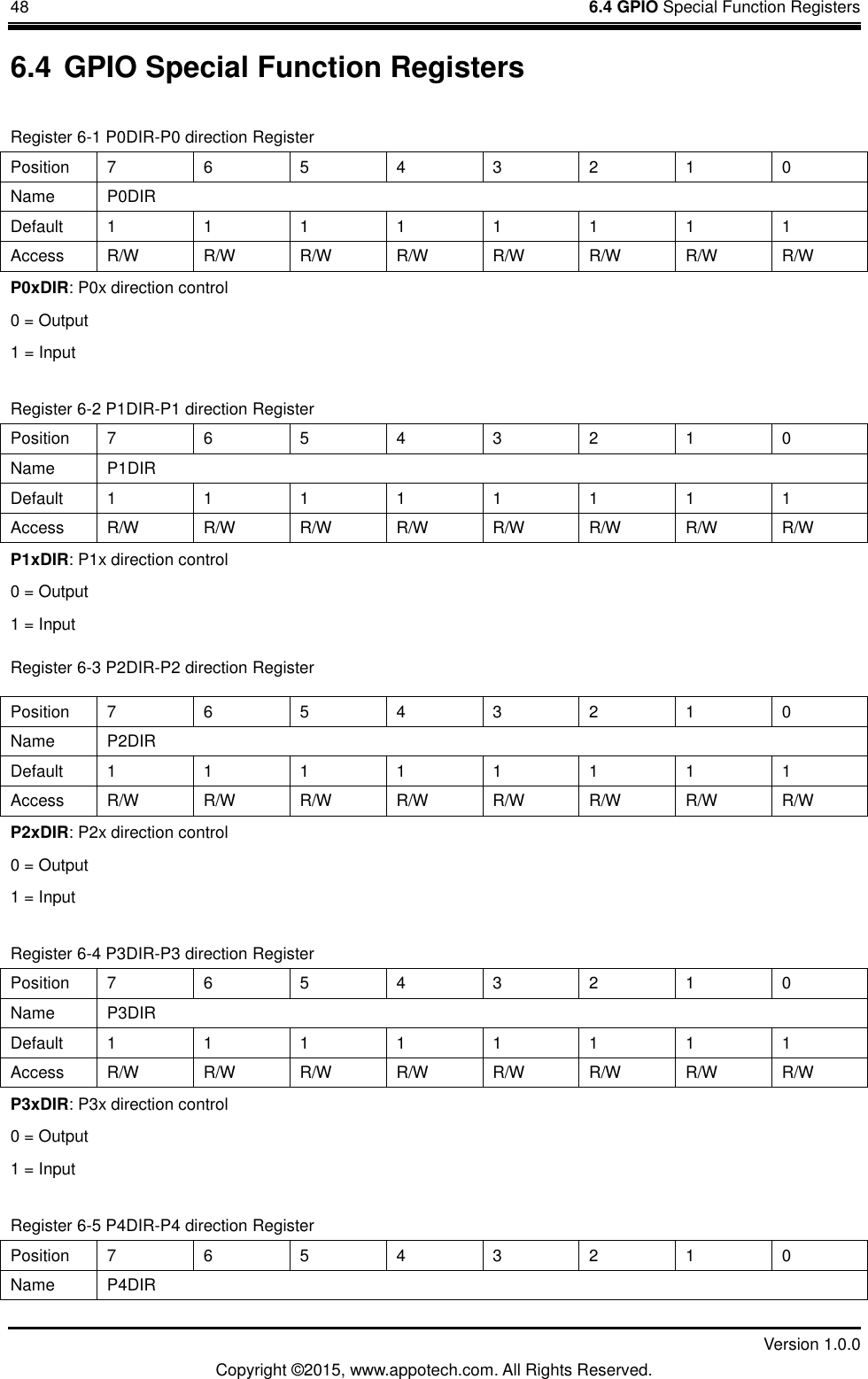
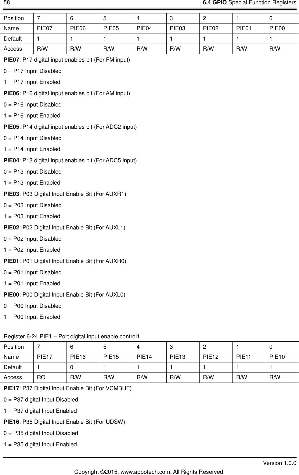
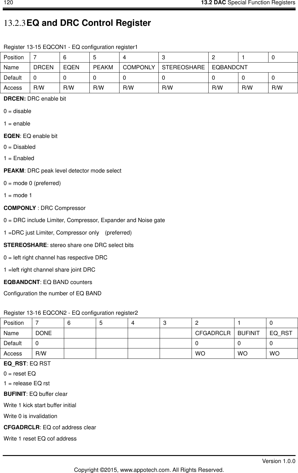
![26 4.2 System Reset Version 1.0.0 Copyright ©2015, www.appotech.com. All Rights Reserved. Watchdog resetPOR resetLVD reset System ResetORPort wakeup resetRTCC reset Figure 4-2 Reset Sources 4.2.1 LVD CW6687B provides 4 levels programmable Low Voltage Detector (LVD) for user to detect VDDLDO power supply voltage or external pin voltage multiplexed with GPIO P2.2. This is because VDDLDO is the input voltage source for on-chip Low-Drop-Out regulator (LDO) which supplies power to internal VDDCORE. Hence, users can momentarily monitor the VDDLDO power if it‟s externally connected to some batteries and for detection if the external power source starts dropping to a level that CW6687B LDO can neither tolerate nor perform properly in the system program. LVD can also be used to monitor external voltage source through the GPIO P2.2 to enhance programmability for different voltage levels. One example of this is it can be used to monitor external power sources or batteries voltage or some voltages related to say pressure or temperature. It is there to provide a simple interface compared to ADC since ADC requires more programming space and procedures to detect precise voltage level in detail. If the user requires general voltage detection without fine voltage range, LVD will be a good choice compared to ADC measurement. XTable 4-1X illustrates different voltage detection levels. Remark: When LVD_ENB is enabled, there is approximately 100us for the band-gap and the comparator to be stable before the end-user can use it as low voltage detection. During the time, LVD_OEB has to be H in order to disable the LVD output which possibly fluctuates signal level. Different power supply falling times will affect the voltage detection. It is recommended that the power supply falling time should be larger than 1ms for stable low voltage detection. When detection occurs, interrupt can be generated if LVD interrupt is enabled, or, CW6687B can undergo reset if interrupt is disabled. Note that the detection is slightly dependent on power supply‟s falling rate and during power drop, noise fluctuation may alter the detection results. For this reason, internally the comparator has about 150mV hysteresis voltage level defined as VHYS = VLVDR-VLVDS to filter out any noise that may occur. Also, the detection level may have a maximum of 100mV difference compared to the value stated in Table 4-1X Table 4-1 LVD level setting BORS[3:0] Detected VDDLDO V BORS[3:0] Detected VDDLDO V 4'b0000 2.200 4'b1000 3.267](https://usermanual.wiki/Yale-Electronics/B922BL/User-Guide-3812035-Page-34.png)
![4 Reset Generation 27 Version 1.0.0 Copyright ©2015, www.appotech.com. All Rights Reserved. BORS[3:0] Detected VDDLDO V BORS[3:0] Detected VDDLDO V 4'b0001 2.333 4'b1001 3.400 4'b0010 2.467 4'b1010 3.533 4'b0011 2.600 4'b1011 3.667 4'b0100 2.733 4'b1100 3.800 4'b0101 2.867 4'b1101 3.933 4'b0110 3.000 4'b1110 4.067 4'b0111 3.133 4'b1111 4.200 For an ideal operation, it is recommended to perform the following for LVD. 1. Select either VDDLDO or external pin to be monitored. Set VD1_ENB = 0 for VDDLDO or VD2_ENB = 0 for external pin 2. Select the detection voltage by setting bits BORS[3:0] 3. Enable the LVD by setting LVD_ENB = 0 4. Wait for at least 30us for the internal band-gap and comparator to become stable 5. Enable the LVD output by setting LVD_OEB = 0 6. The EX_PIN detect voltage must be less than VDDIO Register 4-1 LVDCON– LVD control Position 7 6 5 4 3 2 1 0 Name LVDIF LVDRSTEN LVDOE Default 0 1 0 0 1 0 0 0 Access R/W R/W R/W R/W R/W R/W R/W R/W LVDIF: LVD interrupt pending bit. 0 = When LVD threshold not detect. Cleared by writing a 0 to it 1 = When LVD threshold is detected LVD_RSTEN: LVD Reset enable bit. Low active 0 = LVD Reset is disabled 1 = LVD is enabled LVD_EN: LVD enable bit. Low active 0 = LVD is enabled 1 = LVD is disabled LVD_OE: LVD output enable bit. Low active 0 = LVD output is enabled 1 = LVD output is disabled VD2_EN: External pin (P0.0) voltage enable bit. Low active 0 = External pin voltage detection is enabled 1 = External pin voltage detection is disabled VD1_EN: VDDLDO voltage enable bit. Low active 0 = VDDLDO voltage detection is enabled 1 = VDDLDO voltage detection is disabled](https://usermanual.wiki/Yale-Electronics/B922BL/User-Guide-3812035-Page-35.png)
![28 4.3 Clock System Version 1.0.0 Copyright ©2015, www.appotech.com. All Rights Reserved. LVDS: Voltage detection level select 00 = 2.2V/1.2V 01 = 2.4V/1.95V 10 = 2.7V/2.2V 11 = 3.1V/2.5V 4.2.2 RTCC Reset CW6687B can be reset by RTCC second and alarm interrupt when IRTRSTEN bit in RTCON is set to 1. 4.2.3 Watchdog Reset If Watchdog timer is enabled, and WDTCON [5] is not written by 1 within watchdog overflow time period, CW6687B will be reset by Watchdog overflow. 4.2.4 Port Wakeup Reset During SLEEP mode, port wakeup event will cause CW6687B to reset. 4.3 Clock System 4.3.1 Clock Control CW6687B embeds 32K/4M/12M/24M OSC internal oscillator circuits. External crystal is needed to generate a clock source. One internal PLL can generate 48MHz from the crystal clock source. One internal RC oscillator is also embedded. To make sure the USB module operates properly, the USB clock must be set to 48MHz. In this case, system clock can be 48 MHz or 24MHz. Register 4-2 PCON0 – Power control 0 Position 7 6 5 4 3 2 1 0 Name DRAMCEN IRAMCEN IROMCEN RAM2CEN IRCEN IDLE HOLD SLEEP Default 0 0 0 0 0 0 0 0 Access R/W R/W R/W R/W R/W R/W R/W R/W DRAMCEN: DECRAM clock enable 0 = Enable 1 = Disable IRAMCEN: IRAM clock enable 0 = Enable 1 = Disable IROMCEN: IROM clock enable 0 = Enable 1 = Disable](https://usermanual.wiki/Yale-Electronics/B922BL/User-Guide-3812035-Page-36.png)
![4 Reset Generation 33 Version 1.0.0 Copyright ©2015, www.appotech.com. All Rights Reserved. 00 = 256 X system clock 01 =128 X system clock 10 = 16 X system clock 11 = 2 X system clock 1 = enter low power mode Register 4-9 CLKCON – Clock control Position 7 6 5 4 3 2 1 0 Name Reserved RCSEL WDTCSEL RTCCS SCSEL Default 0 0 0 0 0 0 0 0 Access R/W R/W R/W R/W R/W R/W R/W R/W RCSEL: RC frequency select 00 = RC 512K 01 = RC 32K 10 = RC 1M 11 = RC 4M or XOSC26M controlled by CLKCON2[3] WDTCSEL: WDT clock section 0 = Internal 32 KHz RC oscillator output 1 = External 32 KHz or 12MHz crystal oscillator controlled by CLKCON2 [6] and CLKCON2 [7] RTCCS: RTCC clock source select 00 = External 32 KHz or 12MHz crystal oscillator controlled by CLKCON2 [6] and CLKCON2 [7] 01 = Internal 32 KHz RC oscillator output 10 = Select 32 KHz clock source derived from external 12MHz crystal oscillator 11 = Reserve SCSEL: System clock select 00 = Internal 512 KHz RC oscillator output 01 = External 32 KHz or 12MHz crystal oscillator controlled by PCON3 [5] 10 = PLL 48/24/16/12 MHz output, controlled by CLKCON1 [1:0] 11 = Reserve Register 4-10 CLKCON1 – Clock control 1 Position 7 6 5 4 3 2 1 0 Name ATCLKSEL BTPLL_SEL DECDIV SYSDIV PLLDIVSEL Default 0 0 0 0 0 0 0 0 Access R/W R/W R/W R/W R/W R/W R/W R/W ATCLKSEL: Audio clock select 00 = Select external 12MHz crystal oscillator invert 01 = Select external 12MHz crystal oscillator 10 = Select PLL 24MHz output invert 11 = Select PLL 24MHz output](https://usermanual.wiki/Yale-Electronics/B922BL/User-Guide-3812035-Page-41.png)
![4 Reset Generation 35 Version 1.0.0 Copyright ©2015, www.appotech.com. All Rights Reserved. 00 = 1MHz PLL 01 = 1MHz RC 10 = External 32 KHz or 12MHz crystal oscillator controlled by CLKCON2 [6] and CLKCON2 [7] as shown in X 11 = 1MHz div form XOSC26M 4.3.2 Operation Guide User guide 1: CW6687B integrates a 4M RC clock called RC4M, extern OSC 26MHz, extern OSC 32K or 12MHz 4.3.3 Clock Gating CW6687B provides comprehensive clock gating options for eliminating power-wasting activities. System clock supplies clock signal to different clock domains. Every clock can be gated. It allows the user to shut down the clock signal when the function is not needed. 4.3.4 Phase Lock Loop (PLL) CW6687B provides one on-chip Phase Locked Loop (PLL 48M) clock generators. The PLL has a reference clock from external 32 KHz/4M/12 M crystal oscillators to provide a stable reference clock, and the reference clock is multiplied to provide the final PLL output. Register 4-12 PLLCON – PLL Configuration Position 7 6 5 4 3 2 1 0 Name SDADCLKEN PLLTCLKSEL SDADCCLK_SEL PLL12DREF_SEL PLL1 DREF_SEL Default 0 0 0 0 0 0 0 0 Access R/W R/W R/W R/W R/W R/W R/W R/W PLL1AREF_SEL: PLL1 input reference clock digital select 00 = XOSC 01 = RCOSC 10 = RCOSC div 11 = Reserved PLL2AREF_SEL: PLL2 input reference clock digital select 00 = XOSC 01 = RCOSC 10 = PLL1 div 11 = Reserved SDADCCLK_SEL: SDADC clockl select 00 = XOSC inv 01 = XOSC 10 = PLL2 div2 inv 11 = PLL2](https://usermanual.wiki/Yale-Electronics/B922BL/User-Guide-3812035-Page-43.png)
![38 4.3 Clock System Version 1.0.0 Copyright ©2015, www.appotech.com. All Rights Reserved. PLL2AREF_SEL: PLL2 input reference clock analog select 00 = 12M XOSC 01 = 4M XOSC 10 = 32K XOSC 11 = 32K XOSC PLL2TSEL: PLL2 test select 0 = PLL2 refclock output 1 = PLL2 fbclock output Register 4-19 PLL2INTH – PLL2 integer high Position 7 6 5 4 3 2 1 0 Name PLL2INT[11:8] Default 0 0 0 0 1 0 1 1 Access R/W R/W R/W R/W R/W R/W R/W R/W Register 4-20 PLL2INTL – PLL2 integer low Position 7 6 5 4 3 2 1 0 Name PLL2INT[7:0] Default 1 0 1 0 1 0 0 0 Access R/W R/W R/W R/W R/W R/W R/W R/W PLL2INT = int(98.304MHz/pll2_refclock) Register 4-21 PLL2FRACH – PLL2 fraction high Position 7 6 5 4 3 2 1 0 Name FRACH Default 0 0 0 0 0 0 0 0 Access R/W R/W R/W R/W R/W R/W R/W R/W Register 4-22 PLL2FRACL – PLL2 fraction low Position 7 6 5 4 3 2 1 0 Name FRACL Default 0 0 0 0 0 0 0 0 Access R/W R/W R/W R/W R/W R/W R/W R/W When the fraction is less than 0.25, set FOVER=1, and fraction = (fraction+1)/2, integer = (integer-1) When the fraction is more than 0.80, set FOVER=1, and fraction = fraction/2, integer = integer FRAC = fraction*65535 User’s guide: 1. PLL1 frequency division a) PLL1‟s: -input reference clock is f0 (from RC or OSC)](https://usermanual.wiki/Yale-Electronics/B922BL/User-Guide-3812035-Page-46.png)
![6 General Purpose Input/Output (GPIO) 49 Version 1.0.0 Copyright ©2015, www.appotech.com. All Rights Reserved. Default - - 1 1 1 1 1 1 Access - - R/W R/W R/W R/W R/W R/W P4xDIR: P4x direction control 0 = Output 1 = Input Register 6-6 P0 – P0 data register Position 7 6 5 4 3 2 1 0 Name P0 Default x x x x x x x x Access R/W R/W R/W R/W R/W R/W R/W R/W P0[x]: P0x data. Valid when P0x is used as GPIO 0 = P0x is in low state when read and output low at P0x when write 1 = P0x is in high state when read and output high at P0x when write Register 6-7 P1 – P1 data register Position 7 6 5 4 3 2 1 0 Name P1 Default x x x x x x x x Access R/W R/W R/W R/W R/W R/W R/W R/W P1[x]: P1x data. Valid when P1x is used as GPIO 0 = P1x is in low state when read and output low at P1x when write 1 = P1x is in high state when read and output high at P1x when write Register 6-8 P2 – P2 data register Position 7 6 5 4 3 2 1 0 Name P2 Default x x x x x x x x Access W/R W/R W/R W/R W/R W/R W/R W/R P2[x]: P2x data. Valid when P2x is used as GPIO 0 = P2x is in low state when read and output low at P2x when write 1 = P2x is in high state when read and output high at P2x when write Register 6-9 P3 – P3 data register Position 7 6 5 4 3 2 1 0 Name P3 Default x x x x x x x x Access W/R W/R W/R W/R W/R W/R W/R W/R P3[x]: P3x data. Valid when P3x is used as GPIO 0 = P3x is in low state when read and output low at P3x when write 1 = P3x is in high state when read and output high at P3x when write](https://usermanual.wiki/Yale-Electronics/B922BL/User-Guide-3812035-Page-57.png)
![50 6.4 GPIO Special Function Registers Version 1.0.0 Copyright ©2015, www.appotech.com. All Rights Reserved. Register 6-10 P4 – P4 data register Position 7 6 5 4 3 2 1 0 Name P4 Default - - x x x x x x Access - - RO RO W/R W/R W/R W/R P3[x]: P3x data. Valid when P3x is used as GPIO 0 = P3x is in low state when read and output low at P3x when write 1 = P3x is in high state when read and output high at P3x when write Table 6-3 DRVx register setting Register Address Set bit “x” of PxDRV0 as “1” Clear bit “x” of PxDRV0 as “0” Initial value P0DRV0 R/W Driving is 24mA Driving is 8mA 00h P1DRV0 R/W Driving is 24mA Driving is 8mA 00h P2DRV0 R/W Driving is 24mA Driving is 8mA 00h P3DRV0 R/W Driving is 24mA Driving is 8mA 00h P4DRV0 R/W Driving Driving is 8mA 00h Table 6-4 PUPx register setting Register Address Set bit “x” of PxPU0 as “1” Clear bit “x” of PxPU0 as “0” Initial value P0PU0 R/W Enable pull-up Disable pull-up 00h P1PU0 R/W Enable pull-up Disable pull-up 00h P2PU0 R/W Enable pull-up Disable pull-up 00h P3PU0 R/W Enable pull-up Disable pull-up 00h P4PU0 R/W Enable pull-up Disable pull-up 00h Table 6-5 PDNx register setting Register Address Set bit “x” of PxPD0 as “1” Clear bit “x” of PxPD0 as “0” Initial value P0PD0 R/W Enable pull-down Disable pull-down 00h P1PD0 R/W Enable pull-down Disable pull-down 00h P2PD0 R/W Enable pull-down Disable pull-down 00h P3PD0 R/W Enable pull-down Disable pull-down 00h P4PD0 R/W Enable pull-down Disable pull-down 00h Register 6–11 P1PUS0– P1 pull up select Position 7 6 5 4 3 2 1 0 Name P17PUS0 P16PUS0 P15PUS0 P14PUS0 P13PUS0 P12PUS0 P11PUS0 P10PUS0 Default 0 0 0 0 0 0 0 0 Access W/R W/R W/R W/R W/R W/R W/R W/R Register 6–12 P1PUS1– P1 pull up select Position 7 6 5 4 3 2 1 0](https://usermanual.wiki/Yale-Electronics/B922BL/User-Guide-3812035-Page-58.png)
![7 Timers 73 Version 1.0.0 Copyright ©2015, www.appotech.com. All Rights Reserved. Position 7 6 5 4 3 2 1 0 Name T3CNT Default 0 0 0 0 0 0 0 0 Access R/W R/W R/W R/W R/W R/W R/W R/W Note: Timer3 will increase in proper condition while it is enabled. It overflows when TMR3CNT = TMR3PR, TMR3CNT will be clear to 0x00 when overflow occurs, and the interrupt flag will be set „1‟ by hardware. Register 7-17 TMR3PR – Timer3 Period Position 7 6 5 4 3 2 1 0 Name TMR3PR Default 1 1 1 1 1 1 1 1 Access WO WO WO WO WO WO WO WO Note: The overflow period of the timer is: Tinc-source * T3PSR * (T3PR + 1). Register 7-18 TMR3PWM – Timer3 PWM duty Position 7 6 5 4 3 2 1 0 Name TMR3PWM Default x x x x x x x x Access R/W R/W R/W R/W R/W R/W R/W R/W Note: TMR3PWM is reserved in timer/counter mode. In PWM mode, it is used as duty cycle setting. In capture mode, the value of TMR3CNT will be captured to TMR3PWM when selected event occurs. 7.5 Watchdog Timer (WDT) The Watchdog Timer (WDT) logic consists of a 20bit Watchdog Timer. An internal RC oscillator running at 32 KHz clocks the Watchdog Timer. When device resets, the WDT is disabled and user should enable the WDT if it is needed. In the default configuration, WDT overflows in 2ms. The application program needs to write a „1‟ into WDTCON [5] at least once 2 ms to prevent WDT time out. The lower 3 bits of the WDTCON register control the selection of overflow time period. 7.5.1 Watchdog Wake up WDT can be used to wake up CW6687B from Idle, Hold or Sleep mode. RSTEN bit (WDTCON [3]) is used to determine the actions after WDT wake up. When RSTEN is set to 0, the watchdog will generate a non-reset wake up after counter overflows. And When RSTEN is set to 1, the watchdog will wake up CW6687B by resetting the whole chip. After non-reset wake up CW6687B will continue to execute next instruction. During Idle mode, CW6687B can perform wakeup by WDT with interrupt or reset. During Hold mode, CW6687B perform wakeup by WDT with interrupt or reset or just continue to execute the next instruction. During Sleep mode, CW6687B perform wakeup by WDT with reset. During Deep Sleep mode, CW6687B cannot achieve wakeup by WDT.](https://usermanual.wiki/Yale-Electronics/B922BL/User-Guide-3812035-Page-81.png)
![78 7.6 Independent Power Real Time Clock Counter (IRTCC) Version 1.0.0 Copyright ©2015, www.appotech.com. All Rights Reserved. 0 = Disable 1 = Enable Register 7-21 IRTCDAT – RTCC communication data Position 7 6 5 4 3 2 1 0 Name IRTCDAT Default x x x x x x x x Access R/W R/W R/W R/W R/W R/W R/W R/W Write to IRTCDAT will start IRTCC communication and set DONE flag to 1. Read IRTCDAT will return IRTCC data. Register 7-22 SECCNT –IRTCC timer conter Position 7 6 5 4 3 2 1 0 Name SECCNT7 SECCNT6 SECCNT5 SECCNT4 SECCNT3 SECCNT2 SECCNT1 SECCNT0 Default x x x x x x x x Access WO WO WO WO WO WO WO WO RTCC second counter Register 7-23IRTCON1 – RTCC control1 Position 7 6 5 4 3 2 1 0 Name - - - - RTC_POR IRTC_POR_EN TIMER TIMERIE Default - - - - 0 0 0 Access - - - - R/O R/W R/W R/W RTC_POR: RTCC POR bit 0 = RTCC POR is 0 1 = RTCC POR is 1 NOTE: only design specification can be known. IRTC_POR_EN: IRTCC POR reset system clock enable 0 = Disable 1 = Enable TIMER: Timer pending 0 = No pending (Write 0 to clear pending) 1 = When SECCNT equal to internal counter TIMERIE: Timer pending interrupt enable 0 = Disable 1 = Enable Register 7-24 RANDOM_CNT – random center regent Position 7 6 5 4 3 2 1 0 Name RANDOM_CNT[7:0] Default - - - - - - - -](https://usermanual.wiki/Yale-Electronics/B922BL/User-Guide-3812035-Page-86.png)
![80 7.6 Independent Power Real Time Clock Counter (IRTCC) Version 1.0.0 Copyright ©2015, www.appotech.com. All Rights Reserved. Register 7-26 RTCC3 - RTCC configure register3 Position 7 6 5 4 3 2 1 0 Name - - - DRSEL Default - - - 0 0 0 0 0 Access - - - WO WO DRSEL: IRTCC OSC drive select Register 7-27 PWRCON - Power control register Position 7 6 5 4 3 2 1 0 Name PD_FLAG BIAS_SEL BUCK_MODE_SEL RVDD_EN DVDD_EN VDDIO_EN PMU_EN Default 1 1 1 0 0 0 0 0 Access R/W R/W R/W R/W R/W R/W R/W R/W PD_FLAG: Power down flag BIAS_SEL [1:0]: LDO amp bias current selection 00 = X0 01 = X1 10 = X2, default 11 = X4 BUCK_MODE_SEL: PMU mode select bit 0 = LDO mode 1 = BUCK mode RVDD_EN: RVDD enable bit 0 = enable 1 = disable DVDD_EN: DVDD enable bit 0 = enable 1 = disable VDDIO_EN: VDDIO enable bit 0 = enable 1 = disable PMU_EN: PMU enable bit 0 = enable 1 = disable Register 7-28 WKOCON - WKO control register Position 7 6 5 4 3 2 1 0 Name WKPIN_STA FLTEN ALMOE WKOEN WKOUTEN WKOINEN ALMEN DCIN_WKEN Default 0 0 0 0 0 0 0 0 Access R/W W/R W/R W/R W/R W/R R/W R/W WKPIN_STA: Wake up pin output state](https://usermanual.wiki/Yale-Electronics/B922BL/User-Guide-3812035-Page-88.png)
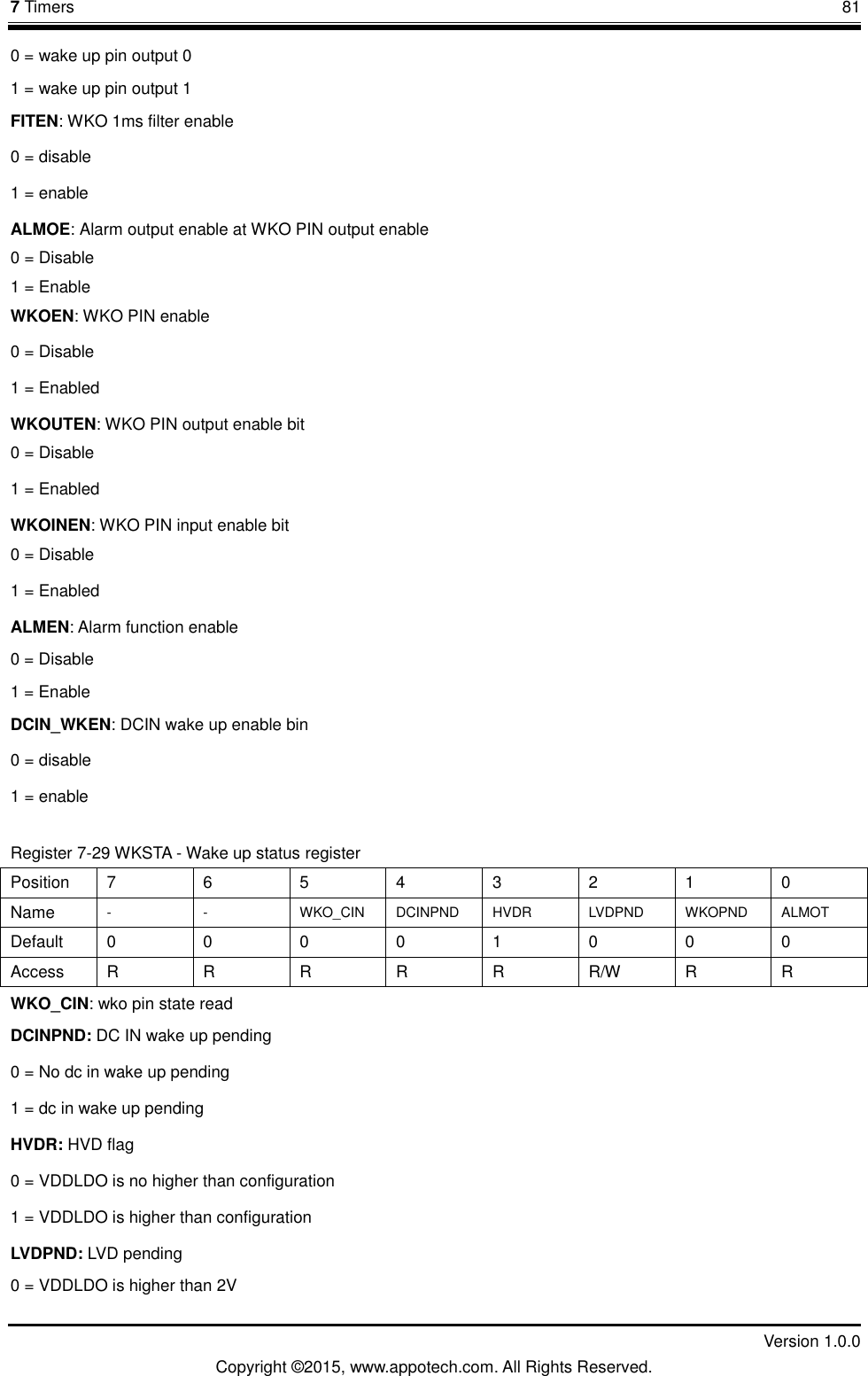
![82 7.6 Independent Power Real Time Clock Counter (IRTCC) Version 1.0.0 Copyright ©2015, www.appotech.com. All Rights Reserved. 0 = VDDLDO is lower than 2V Write this bit 0 will clear LVDPND WKOPND: IRTWKO wake up pending 0 = No wakeup 1 = IRTWKO pin wake up pending ALMOT: Alarm match flag. 0 = No alarm match happen 1 = Alarm match This flag is set to „1‟ by hardware when alarm register match real timer counter. It can be clear to „0‟ of ALMEN is set to „0‟ or „Write_ALM‟ is detected. Register 7-30 VCL VOLTAGE configure register Position 7 6 5 4 3 2 1 0 Name SC_RTC[4] SC_RTC[3] SC_RTC[2] SC_RTC[1] SC_RTC[0] HVDS HVDEN LVDEN Default 1 1 0 1 0 0 0 0 Access W/R W/R W/R W/R W/R W/R W/R W/R SC_RTC [4]: OSCO OSCI capacitance select SC_RTC [3:2]: OSCO capacitance select SC_RTC [1:0]: OSCI capacitance select HVDS: HVD level select 0 = 4.0V 1 = 4.2V LVDEN: LVD enable bit 0 = Disabled 1 = Enabled In IRTCC timer, there is one 32-bit real time counter. The unit of this counter is per second. If display the time on LCD, you should convert to second, minute, hour, date and so on. When use “Write_RTC” command to config this counter, the fisrt byte is config the highest counter, and the forth byte is config the lowest counter. When use “Read_RTC” command to read this counter, the first byte output is the highest counter, and the forth byte output is the lowest counter. In IRTCC timer, there is one 32-bit alarm register. The unit of this counter is per second. If display the time on LCD, you should convert to second, minute, hour, date and so on. When use “Write_ALM” command to config this counter, the fisrt byte is config the highest counter, and the forth byte is config the lowest counter. When use “Read_ALM” command to read this counter, the first byte output is the highest counter, and the forth byte output is the lowest counter. 7.6.6 IRTCC Operating Guide ;-------------------------------- ; Write RTC Config Write_Cfg: ORL IRTCON, #(1<<0) ;RTC enable](https://usermanual.wiki/Yale-Electronics/B922BL/User-Guide-3812035-Page-90.png)
![90 8.1 UART0 Version 1.0.0 Copyright ©2015, www.appotech.com. All Rights Reserved. RXIF: RX Interrupt Flag 0 = RX not done 1 = RX done TXIF: TX Interrupt Flag 0 = TX not done 1 = TX done Writing data to UTBUF will clear this flag. PSEL: UART0 Port Select 0 = Select UART0RX0 and UART0TX0 UART0RX0: P34 UART0TX0: P16 1 = Select UART0RX1 and UART0TX1 UART0RX1: P00 UART0TX1: P01 Register 8-3 UARTBAUDL – UART0 Baud Rate Low Byte Position 7 6 5 4 3 2 1 0 Name UARTBAUDL Default x x x x x x x x Access WO WO WO WO WO WO WO WO Register 8-4 UARTBAUDH – UART0 Baud Rate High Byte Position 7 6 5 4 3 2 1 0 Name UARTBAUDH Default 0 0 0 0 0 0 0 0 Access WO WO WO WO WO WO WO WO UARTBAUD = {UARTBAUDH, UARTBAUDL} Register 8-5 UARTDIV Position 7 6 5 4 3 2 1 0 Name UARTDIV Default 0 0 0 0 0 0 0 0 Access WO WO WO WO WO WO WO WO Baud Rate =Fsys clock / [(UARTBAUD +1) x (UARTDIV + 1)] Register 8-6 UARTDATA – UART0 Data Position 7 6 5 4 3 2 1 0 Name UARTDATA Default x x x x x x x x Access R/W R/W R/W R/W R/W R/W R/W R/W Write this location will load the data to transmitter buffer. And read this location will read the data from the receiver](https://usermanual.wiki/Yale-Electronics/B922BL/User-Guide-3812035-Page-98.png)
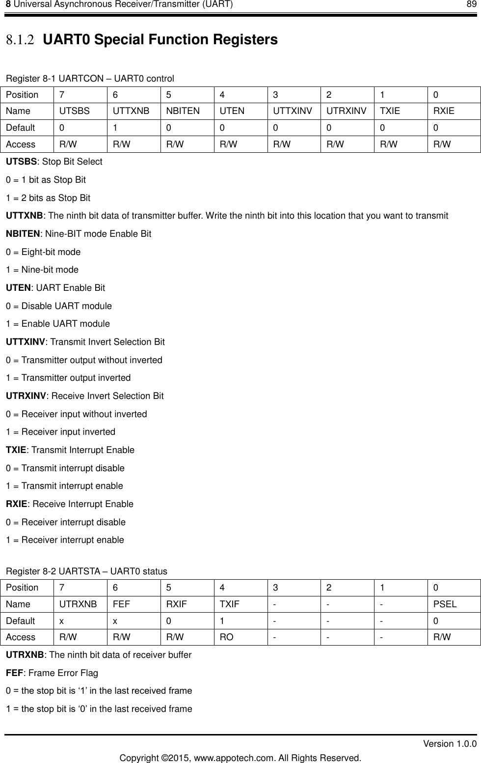
![8 Universal Asynchronous Receiver/Transmitter (UART) 91 Version 1.0.0 Copyright ©2015, www.appotech.com. All Rights Reserved. buffer. 8.2 UART1 8.2.1 Overview UART1 is a serial port capable of asynchronous transmission. The UART1 can function in normal and DMA full duplex mode. Please sees PMUXCON0 bit 6 descriptions when PMUXCON0[6] == 0 Receive pin (RX) – UART1RX0 (P17) Transmit pin (TX) – UART1TX0 (P16) Or PMUXCON0[6] == 1 Receive pin (RX) – UART1RX1 (BT_TX) Transmit pin (TX) – UART1TX1 (BT_RX) 8.2.2 UART1 Special Function Registers Register 8-7 UART1CON – UART1 control Position 7 6 5 4 3 2 1 0 Name UTSBS UTTXNB NBITEN UTEN TXIE RXIE OVERFLOWIE DMASEL Default 0 1 0 0 0 0 - 0 Access R/W R/W R/W R/W R/W R/W - R/W UTSBS: Stop Bit Select 0 = 1 bit as Stop Bit 1 = 2 bits as Stop Bit UTTXNB: The ninth bit data of transmitter buffer. Write the ninth bit into this location that you want to transmit NBITEN: Nine-BIT mode Enable Bit 0 = Eight-bit mode 1 = Nine-bit mode UTEN: UART Enable Bit 0 = Disable UART module 1 = Enable UART module TXIE: Transmit Interrupt Enable 0 = Transmit interrupt disable 1 = Transmit interrupt enable RXIE: Receive Interrupt Enable 0 = Normal Receive interrupt disable or AUTO DMA mode Receive one word Interrupt disable 1 = Normal Receive interrupt enable or AUTO DMA mode Receive one word Interrupt enable OVERFLOWIE: Receive DMA overflow interrupt enable 0 = overflow Interrupt disable](https://usermanual.wiki/Yale-Electronics/B922BL/User-Guide-3812035-Page-99.png)
![96 8.4 BT Control Register Version 1.0.0 Copyright ©2015, www.appotech.com. All Rights Reserved. 8.4 BT Control Register Register 8-21 BTCON1 – BT control register1 Position 7 6 5 4 3 2 1 0 Name BTC2RS BTCDCLKO BTCDCLKI BTRSTB Reserved XOSC26MEN Default 0 0 0 0 0 0 0 0 Access R/W R/W R/W RO R/W R/W R/W R/W BTC2RS: BTCON2 read select 0 = read BTCONT register 1 = read BT output state BTCDCLKO: BT CDCLK output state BTCDCLKI: BT CDCLK input state XOSC26MEN: BT xosc26M enable 0 = disable 1 = enable Register 8-22 BTCON2 – BT control register2 Position 7 6 5 4 3 2 1 0 Name BTTX BTRX BTCTS BTTESTEN BTGPIO10 BTGPIO9 BTGPIO5 BTGPIO4 Default 0 0 0 0 0 0 0 0 Access R/W R/W R/W R/W R/W R/W R/W R/W write: write date to BT read: depend on BTCON1[5]](https://usermanual.wiki/Yale-Electronics/B922BL/User-Guide-3812035-Page-104.png)
![11 SPI 103 Version 1.0.0 Copyright ©2015, www.appotech.com. All Rights Reserved. 11 SPI 11.1 SPI0 SPI0 can serve as master or slave. It can operate in normal or DMA mode. SPI0 map to three group ports configured by PWKEDGE[6] and SPICON[3]: Group0 - P27, P25, P26; Group1 - P04, P06, P05; Group2 - P14, P00, P34. Group3 - P30(P40), P31, P32 When PWKEDGE[6]=0 and SPI0CON.3 = 0, Group0 activated 2wire mode: P2.6 as SPI0CLK0, P2.7 as SPI0DIDO0; 3wire mode: P2.6 as SPI0CLK0, P2.7 as SPI0DO2, P2.5 as SPI0DI0. When PWKEDGE[6]=0 and SPI0CON.3 = 1, Group1 activated 2wire mode: P0.5 as SPI0CLK1, P0.4 as SPI0DIDO1; 3wire mode: P0.5 as SPI0CLK1, P0.4 as SPI0DO1, P0.6 as SPI0DI1. When PWKEDGE[6]=1 and SPI0CON.3 = 0 Group2 activated 2wire mode: P3.4 as SPI0CLK2, P1.4 as SPI0DIDO2; 3wire mode: P3.4 as SPI0CLK2, P1.4 as SPI0DO2, P0.0 as SPI0DI2. When PWKEDGE[6]=1 and SPI0CON.3 = 1, Grop3 activated 2wire mode: P3.0 as SPI0CLK3, P3.2 as SPI0DIDO3; 3wire mode: P3.0 as SPI0CLK3, P3.2 as SPI0DO3, P3.1 as SPI0DI3. when PMUXCON0[5] = 1 P4.0 as SPI0CLK3 11.1.1 SPI0 Special Function Registers Register 11-1 SPI0CON – SPI0 control Position 7 6 5 4 3 2 1 0 Name SPI0PND SPI0SM SPI0RT SPI0WS SPI0PS0 SPI0EDGE SPI0IDST SPI0EN Default 1 0 0 0 0 0 0 0 Access RO R/W R/W R/W R/W R/W R/W R/W SPI0PND: SPI0 Pending bit (read only, writing SPI0BUF will clear this bit) 0 = Transmission is not finish 1 = Transmission finish](https://usermanual.wiki/Yale-Electronics/B922BL/User-Guide-3812035-Page-111.png)
![104 11.1 SPI0 Version 1.0.0 Copyright ©2015, www.appotech.com. All Rights Reserved. SPI0SM: SPI0 mode selection 0 = Master mode 1 = Slave mode SPI0RT: SPI0 RX/TX select bit in 2-wire mode or DMA mode 0 = TX 1 = RX In 3-wire mode, SPI0 can both Transmit and receive at the same time. But when using DMA mode or 2-wire mode, just one direction (TX or RX) is allowed. Use this bit to select TX or RX. SPI0WS: SPI0 2-wire mode/3-wire mode select bit 0 = 3-wire mode 1 = 2-wire mode SPI0PS0: SPI0 Port select 0 0 = Select P27, P25, P26 when SPI0PS1 = 0; Select P14, P00, P34 when SPI0PS1 = 1 1 = Select P04, P06, P05 when SPI0PS1 = 0 SPI0EDGE: SPI0 sampling edge select bit When SPI0IDST = 0: 0 = Sample at falling edge 1 = Sample at rising edge When SPI0IDST = 1: 0 = Sample at rising edge 1 = Sample at falling edge SPI0IDST: SPI0 clock signal idle state 0 = Clock signal stays at 0 when idle 1 = Clock signal stays at 1 when idle SPI0EN: SPI0 enable bit 0 = SPI0 disable 1 = SPI0 enable Register 11-2 SPIBAUD – SPI0 Baud Rate Position 7 6 5 4 3 2 1 0 Name SPIBAUD Default x x x x x x x x Access WO WO WO WO WO WO WO WO Baud rate = Fsystem_clock / [2(SPIBAUD+1)] Register 11-3 SPI0BUF – SPI0 Data Buffer Position 7 6 5 4 3 2 1 0 Name SPI0BUF Default x x x x x x x X Access R/W R/W R/W R/W R/W R/W R/W R/W](https://usermanual.wiki/Yale-Electronics/B922BL/User-Guide-3812035-Page-112.png)
![112 12.1 EMI Control Registers Version 1.0.0 Copyright ©2015, www.appotech.com. All Rights Reserved. EMIBUF is the entrance of 6 bytes EMI output buffer. The 6 bytes EMI output buffer is emibuf0, emibuf1, emibuf2, emibuf3, emibuf4 and emibuf5. When CPU writes to EMIBUF, internal counter will add “1”, CPU data is pushed to corresponding buffer. You should clear internal counter by writing “0” to emicon1 bit 7; PWM mode: should write eight times for eight channels PWM of P2 When EMIM = 0, emibuf0 will output to P2. Emibuf0 is updated with CPU write data. When EMIM = 1 and in no convert mode, emibuf0 will output to P2. Emibuf0 is updated with SPI1 DMA data. When SPI2EMI = 1 and in convert mode, there are 3 output modes: Register 12-4 PMWBUF0/1/2/3/4/5/6/7 – PWM duty buffer0/1/2/3/4/5/6/7 Position 7 6 5 4 3 2 1 0 Name PWMBUF0/1/2/3/4/5/6/7 Default x x x x x x x x Access WO WO WO WO WO WO WO WO This register confige PWM duty. PWM period is config by EMICON0[3:0] and EMICON0[6:4]. PWM period = pre counter * post counter * system clock EMICON0[6:4]: config pwm output period post counter 000 = 2 001 = 4 010 = 8 011 = 16 100 = 32 101 = 64 110 = 128 111 = 256 EMICON0[3:0]: config pwm output period pre counter 0xxx = 1 1000 = 2 1001 = 4 1010 = 8 1011 = 16 1100 = 32 1101 = 64 1110 = 128 1111 = 256 Corresponding bit 0 1 1 byte mode emibuf0 emibuf3](https://usermanual.wiki/Yale-Electronics/B922BL/User-Guide-3812035-Page-120.png)
![13 Audio Terminal (DAC) 123 Version 1.0.0 Copyright ©2015, www.appotech.com. All Rights Reserved. Rout = Lin* DACLRMIX2/128 + Rin* DACLRMIX3/128 Register 13-22 DACLRMIX3 DAC L & R channel mixing coefficient 3 Position 7 6 5 4 3 2 1 0 Name DACLRMIX3 Default 0 1 1 1 1 1 1 1 Access RW RW RW RW RW RW RW RW DAC L & R channel mixing coefficient register 3 NOTE: DACLRMIX2 and DACLRMIX3 are used to control how R channel is combined with L channel to generate the final R channel output. The content of DACLRMIX2 and DACLRMIX3 each represents a 8 bit signed number which ranges from -128 ~ 127. the R channel output is calculated from the following equation: Rout = Lin* DACLRMIX2/128 + Rin* DACLRMIX3/128 Register 17-28 KVCCON– Key Voice control Position 7 6 5 4 3 2 1 0 Name - - - - - - MPEN KEYEN Default x x x x x x 1 0 Access x x x x x x R/W R/W KEY_DMA_ADRH: Key voice DMA high address MPEN: MP3 is playing enable 0 = Disable MP3 play when plays key voice 1 = Enable MP3 play when plays key voice KEYEN: Key Voice enable 0 = Disabled 1 = Enabled Register 17-29 KVCCON2– Key Voice control Position 7 6 5 4 3 2 1 0 Name KVCCYC[4:0] KVV[2:0] Default 0 0 0 0 1 1 1 1 Access R/W R/W R/W R/W R/W R/W R/W R/W KVCCON2: key voice control KVV [2:0]: key voice volume control 000 = volume div 128 001 = volume div 64 010 = volume div 32 011 = volume div 16 100 = volume div 8 101 = volume div 4 110 = volume div 2 111 = 0db](https://usermanual.wiki/Yale-Electronics/B922BL/User-Guide-3812035-Page-131.png)
![124 13.3 Operation Guide Version 1.0.0 Copyright ©2015, www.appotech.com. All Rights Reserved. KVCCYC [4:0]: key voice plays cycle control The real cycle of key voice play is KVCCYC [4:0] * 8. Register 17-30 KVCADR– Key Voice DMA address Position 7 6 5 4 3 2 1 0 Name KEY_DMA_ADR Default x x x x x x x x Access WO WO WO WO WO WO WO WO When configure key voice DMA address, should write this register three times. First configure the DMA start high address, second configure the DMA start low address, and third configure the DMA end low address. It can only change between 0 to 0xff 13.3 Operation Guide 13.3.1 DAC Operation Guide 1. Configure DACVOLL & DACVOLH 2. Configure DACVCON 3. Clear DACVPND to kick start adjust volume 13.3.2 EQ Operation Guide 1. Configure EQCON2 to release The rest of EQ 2. Configure EQCON1 BIT 6 to kick initiate the buffer ram and wait done 3. Configure EQVOLIN 4. Configure EQCOF to initiate coefficient 5. Configure EQCON1 to enable EQ Notice: 1) If user wants to change the coefficient of EQ he/she must configure EQCON1 disable EQ, then repeat upwards operation guide flow.](https://usermanual.wiki/Yale-Electronics/B922BL/User-Guide-3812035-Page-132.png)
![15 CRC16 /LFSR16/LFSR32 129 Version 1.0.0 Copyright ©2015, www.appotech.com. All Rights Reserved. Register 15-2 CRCFIFO– CRC FIFO control Position 7 6 5 4 3 2 1 0 Name CRCFIFO Default x x x x x x x x Access WO WO WO WO WO WO WO WO Write this location will load the data to CRC module; Register 15-3 CRCRES0– CRC result 0 control Position 7 6 5 4 3 2 1 0 Name CRCRES0 Default x x x x x x x x Access RO RO RO RO RO RO RO RO Register 15-4CRCRES1– CRC result 1 control Position 7 6 5 4 3 2 1 0 Name CRCRES1 Default x x x x x x x x Access RO RO RO RO RO RO RO RO 15.2 LFSR16 15.2.1 Features Software can control lfsr16, or enable CRCEN of SPI1CON1 [1], hardware can auto trigger lfsr16 when spi1 receive data. The LFSR16 polynomial is defined as: 15.2.2 LFSR16 Special Function Register Register 15-5 LFSR16_DAT0– LFSR16 data 0 Position 7 6 5 4 3 2 1 0 Name LFSR16_DAT0 Default 1 1 1 1 1 1 1 1 Access W/R W/R W/R W/R W/R W/R W/R W/R Note: To initiate the LFSR16 register, user needs to write this register 2 times to LFSR16 register for LFSR16 (High byte first). Reading will output LFSR16 data0 Register 15-6 LFSR16_DAT1– LFSR16 data 1 Position 7 6 5 4 3 2 1 0 Name LFSR16_DAT1](https://usermanual.wiki/Yale-Electronics/B922BL/User-Guide-3812035-Page-137.png)
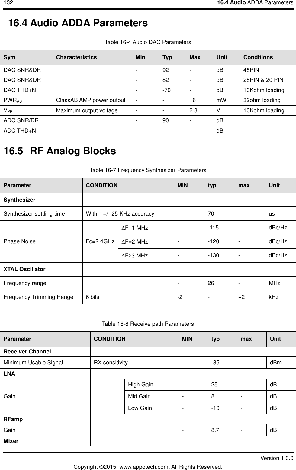
![16 Characteristics 133 Version 1.0.0 Copyright ©2015, www.appotech.com. All Rights Reserved. Parameter CONDITION MIN typ max Unit Conversion Gain - -2.4 - dB IFamp Gain 22/19/16/13 dB - 16 - Complex BPF Band pass -3 dB BW Figure 1. - 2 - MHz Image Rejection - 30 - dB VGA Gain Range -6 - +48 dB Gain Step - +1/+6 - dB ADMOD SNDR Freq = +- BW - >50 - dB Table 16-9 Transmit path Parameters Parameter CONDITION MIN typ max Unit Transmit Channel Available output power -2 0 1.5 dBm Side Band Suppression - -30 - dBm LPF Low pass -3 dB BW - 2 - MHz TXVGA Gain Step 0.5 - 5 dB PA Gain Range Set paPWR[2:0] of Control Register #16 GFSK -12 - 5 dBm DPSK -15 - 2 dBm Note: For each analog RF block register setting, please refer to "BT_EDR_Register_v11l_BT8201AS.xls"](https://usermanual.wiki/Yale-Electronics/B922BL/User-Guide-3812035-Page-141.png)