Yale Electronics B922BL Bluetooth Sport Headset User Manual
Shenzhen Yale Electronics Co., Ltd. Bluetooth Sport Headset
User Manual

B922BL
Bluetooth Sport Headset
User
Manual
Versions:
1.0.0
Release Date: 2015-10-26

Table of content I
Version 1.0.0
Copyright © 2015, www.appotech.com. All Rights Reserved.
Table of content
Table of content ......................................................................................................................................... I
1 Product Overview .............................................................................................................................. 1
1.1 General Description ................................................................................................................... 1
1.2 Features ...................................................................................................................................... 1
2 Pin Definitions ................................................................................................................................... 2
2.1 CW6687B .................................................................................................................................... 2
2.1.1 Package ............................................................................................................................... 2
2.1.2 Pin Assignment ................................................................................................................... 2
2.1.3 Pin Descriptions .................................................................................................................. 3
3 CPU Core Information ....................................................................................................................... 5
3.1 Architecture ............................................................................................................................... 5
3.2 Instruction Set ............................................................................................................................ 5
3.3 Memory Mapping ...................................................................................................................... 8
3.3.1 Program Memory Mapping ................................................................................................ 8
3.3.2 External Data Memory Mapping ........................................................................................ 8
3.3.3 Internal Data Memory Mapping ......................................................................................... 9
3.4 Interrupt Processing ................................................................................................................. 10
3.4.1 Interrupt sources .............................................................................................................. 10
3.4.2 Interrupt Priority............................................................................................................... 12
3.5 Special Function Register Mapping (SFR) ................................................................................. 12
3.6 Extend Special Function Registers Mapping (XSFR) ................................................................. 13
3.7 CPU and Memory related SFR Description .............................................................................. 14
3.8 CPU breakpoint ........................................................................................................................ 23
4 Reset Generation ............................................................................................................................. 25
4.1 Power-on Reset (POR) .............................................................................................................. 25
4.2 System Reset ............................................................................................................................ 25
4.2.1 LVD .................................................................................................................................... 26

II Table of content
Version 1.0.0
Copyright © 2015, www.appotech.com. All Rights Reserved.
4.2.2 RTCC Reset ........................................................................................................................ 28
4.2.3 Watchdog Reset ............................................................................................................... 28
4.2.4 Port Wakeup Reset ........................................................................................................... 28
4.3 Clock System ............................................................................................................................ 28
4.3.1 Clock Control .................................................................................................................... 28
4.3.2 Operation Guide ............................................................................................................... 35
4.3.3 Clock Gating ...................................................................................................................... 35
4.3.4 Phase Lock Loop (PLL) ....................................................................................................... 35
5 Low Power Management ................................................................................................................ 40
5.1 Power Saving Mode ................................................................................................................. 40
5.1.1 Sleep Mode ....................................................................................................................... 40
5.1.2 Hold Mode ........................................................................................................................ 40
5.1.3 Idle Mode .......................................................................................................................... 40
5.1.4 Power Down Mode ........................................................................................................... 41
5.2 Power Supply............................................................................................................................ 41
6 General Purpose Input/Output (GPIO) ............................................................................................ 46
6.1 Overview .................................................................................................................................. 46
6.2 Features .................................................................................................................................... 46
6.3 Function multiplexing ............................................................................................................... 46
6.4 GPIO Special Function Registers .............................................................................................. 48
6.5 Port interrupt and wakeup ....................................................................................................... 63
6.5.1 Wakeup registers .............................................................................................................. 63
6.6 Operation Guide ....................................................................................................................... 65
7 Timers .............................................................................................................................................. 66
7.1 Timer0 ...................................................................................................................................... 66
7.1.1 Timer0 Special Function Registers .................................................................................... 66
7.2 Timer1 ...................................................................................................................................... 67
7.2.1 Timer1 Special Function Registers .................................................................................... 67
7.3 Timer2 ...................................................................................................................................... 69
7.3.1 Timer2 Features ................................................................................................................ 69

Table of content III
Version 1.0.0
Copyright © 2015, www.appotech.com. All Rights Reserved.
7.3.2 Timer2 Special Function Registers .................................................................................... 70
7.4 Timer3 ...................................................................................................................................... 71
7.4.1 Timer3 Features ................................................................................................................ 72
7.4.2 Timer3 Special Function Registers .................................................................................... 72
7.5 Watchdog Timer (WDT) ........................................................................................................... 73
7.5.1 Watchdog Wake up .......................................................................................................... 73
7.5.2 Watchdog SFR ................................................................................................................... 74
7.6 Independent Power Real Time Clock Counter (IRTCC) ............................................................ 75
7.6.1 IRTCC Controller ............................................................................................................... 75
7.6.2 IRTCC Timer ...................................................................................................................... 75
7.6.3 Communication with IRTCC Timer .................................................................................... 75
7.6.4 IRTCC Special Function Registers ...................................................................................... 77
7.6.5 IRTCC components description ........................................................................................ 79
7.6.6 IRTCC Operating Guide ..................................................................................................... 82
8 Universal Asynchronous Receiver/Transmitter (UART) .................................................................. 88
8.1 UART0 ....................................................................................................................................... 88
8.1.1 Overview ........................................................................................................................... 88
8.1.2 UART0 Special Function Registers .................................................................................... 89
8.2 UART1 ....................................................................................................................................... 91
8.2.1 Overview ........................................................................................................................... 91
8.2.2 UART1 Special Function Registers .................................................................................... 91
8.3 Operation Guide ....................................................................................................................... 95
8.4 BT Control Register .................................................................................................................. 96
9 Direct Memory Access (DMA) ......................................................................................................... 97
9.1 DMA for IRAM .......................................................................................................................... 97
9.2 DMA for RAM2 ......................................................................................................................... 97
9.3 DMA for DECRAM ..................................................................................................................... 97
9.4 DMA for IROM .......................................................................................................................... 98
10 IR receiver ........................................................................................................................................ 99
10.1 IR frame format ........................................................................................................................ 99

IV Table of content
Version 1.0.0
Copyright © 2015, www.appotech.com. All Rights Reserved.
10.2 IR Receiver Control Registers ................................................................................................. 100
10.3 IR Receiver Operation Guide .................................................................................................. 102
11 SPI .................................................................................................................................................. 103
11.1 SPI0 ......................................................................................................................................... 103
11.1.1 SPI0 Special Function Registers ...................................................................................... 103
11.1.2 SPI0 Operation Guide ..................................................................................................... 105
11.2 SPI1 ......................................................................................................................................... 106
11.2.1 SPI1 Special Function Registers ...................................................................................... 106
11.2.2 SPI1 Operation Guide ..................................................................................................... 108
12 External Memory Interface (EMI) .................................................................................................. 110
12.1 EMI Control Registers ............................................................................................................. 110
13 Audio Terminal (DAC) .................................................................................................................... 114
13.1 Features .................................................................................................................................. 114
13.2 DAC Special Function Registers .............................................................................................. 114
13.2.1 DAC Register Mapping .................................................................................................... 114
13.2.2 Function of DAC Control Registers ................................................................................. 115
13.2.3 EQ and DRC Control Register .......................................................................................... 120
13.3 Operation Guide ..................................................................................................................... 124
13.3.1 DAC Operation Guide ..................................................................................................... 124
13.3.2 EQ Operation Guide ........................................................................................................ 124
14 SARADC .......................................................................................................................................... 125
14.1 Features .................................................................................................................................. 125
14.2 ADC Pin Mapping.................................................................................................................... 125
14.3 SARADC Special Function Registers........................................................................................ 125
15 CRC16 /LFSR16/LFSR32 ................................................................................................................. 128
15.1 CRC16 ..................................................................................................................................... 128
15.1.1 Features .......................................................................................................................... 128
15.1.2 CRC16 Special Function Registers ................................................................................... 128
15.2 LFSR16 .................................................................................................................................... 129
15.2.1 Features .......................................................................................................................... 129

Table of content V
Version 1.0.0
Copyright © 2015, www.appotech.com. All Rights Reserved.
15.2.2 LFSR16 Special Function Register ................................................................................... 129
15.3 LFSR32 .................................................................................................................................... 130
15.3.1 Features .......................................................................................................................... 130
15.3.2 LFSR32 Special Function Registers .................................................................................. 130
16 Characteristics ............................................................................................................................... 131
16.1 PMU Parameters .................................................................................................................... 131
16.2 CORE PLL Parameters ............................................................................................................. 131
16.3 General purpose I/O Parameters ........................................................................................... 131
16.4 Audio ADDA Parameters ........................................................................................................ 132
16.5 RF Analog Blocks .................................................................................................................... 132
17 Package Outline Dimensions ......................................................................................................... 134
17.1 QFN32..................................................................................................................................... 134
Revision History .......................................................................................................................................... i

1 Product Overview 1
Version 1.0.0
Copyright ©2015, www.appotech.com. All Rights Reserved.
1 Product Overview
Bluetooth Audio Player Microcontroller
1.1 General Description
CW6687B
is a compact, highly integrated system on chip for
Bluetooth v4.2
with Enhanced Data Rate applications.
This SOC complies with Bluetooth specifications and is backward-compatible with Bluetooth 2.1, 2.0 or 1.2 systems.
This
Bluetooth
includes
a
data
rate
of
1M/2M/3Mbps
RF
with
a
performance
of
Tx:
0dBm,
Rx:
-85dBm,
and
full-duplex UART, SPI, interface with EDR applications.
It also integrates a DSP co-processor, a PLL, and a CODEC to provide exceptional voice and audio quality.
In addition, to provide easy accessibility and transferability to other auxiliary products,
1.2 Features
Supports Bluetooth v.4.2+EDR; backward-compatible with BT v.1.2, 2.0 and 2.1
SOC supports following versions:
Hands Free v.1.6
Headset v.1.2
A2DP v.1.3
AVCTP v.1.4
AVDTP v.1.3
AVRCP v.1.5
Class 2 power level, RF Performance: Tx:0dBm, Rx: -85dBm;
Supports 26M crystal with independently powered real-time clock that supports 32.768kHz internal crystal
oscillator
Supports MP3/SBC/WMA decoder;
Three Channels 10-bit SARADC;
Watchdog Timer with on-chip RC oscillator
Supports full-duplex UART, SPI interface;
Keypad tone mixer;
Internal LDO regulator : 1.35V to 1.2V, 5V to 3.3V;
Built-in buck converter,DC-DC 5V to 1.35V ;
Power on Reset
Integrated 24bits DSP core that supports:
Noise suppressor to eliminate unwanted noise and hum without altering enhanced audio quality
Echo cancelation
SBC audio format decoding
Automatic volume control for speaker output
16bit Stereo DAC with >90dB SNR, embedded with 2 class A/B headphone amplifier

2 1.2 Features
Version 1.0.0
Copyright ©2015, www.appotech.com. All Rights Reserved.
16bit Stereo ADC with >90dB DR
Internal charger current up to 25mA
Supports dual MIC
Channels 16 levels Low Voltage Detector

2 2.1 CW6687B
Version 1.0.0
Copyright ©2015, www.appotech.com. All Rights Reserved.
2 Pin Definitions
2.1 CW6687B
2.1.1 Package
QFN32
2.1.2 Pin Assignment
Figure 2-1 X shows the pin assignments of QFN32 package.
CW6687B
QFN32
V1.0
1
2
3
4
5
6
7
8
9
10
31
32
VDDLDO
MICP0
VDDIO/AVDD
USBDM
USBDP
VBUS
VBAT_CHARGER
VDD
IRTCWKO
VDDRTC
11
12
13
14
15
16
MICP1
VCM
VSSADC/VSSDAC
VDDHP
DACL
DACR
VCM_BUF/P01
18
17
20
19
22
21
24
23
MICBIAS/P00
P33
P13
P32
P31
P30
VCC_RF/PAD_VCC_PA
RXTX
29
30
27
28
25
26
VOUT1V5
BVSSP
LX
VBAT
XO_N
XO_P
VCC_VCO/PAD_VDDQ
/RVDD/VCC_XO
Figure 2-1 Pin assignment for QFN32

2 Pin Definitions 3
Version 1.0.0
Copyright ©2015, www.appotech.com. All Rights Reserved.
2.1.3 Pin Descriptions
XTable 2-1 shows the pin descriptions of QFN32 package.
Table 2-1 QFN32 pin description
Pin No.QFN32 Name Type Function
1 VDDIO/AVDD PWR Power output VDDIO 3.3V
2 USBDM I/O USB Negative Input/output
3 USBDP I/O USB Positive Input/output
4 VBUS PWR Charger power input
5 VBAT_CHARGER PWR Charger output to battery
6 VDD PWR Core power VDD 1.2V
7 IRTCWKO I/O RTC wakeup/Solf Power on/off control
pin
8 VDDRTC PWR RTC power
9 MICP0 AI MIC0 Positive input
10 MICP1 AI MIC1 Positive input
11 VCM AO DAC VCM output
12 AVSS GND Audio GND
13 VDDHP PWR Headphone power output
14 VOUTL AI/O DAC left output
GPIO input
15 VOUTR AI/O DAC right output
GPIO input
16 P01/VCM_BUF I/O
GPIO
DAC VCM Buffer
AUXR0
UARTTX1
PORT INT/WKUP0
SDDAT2
17 P00/MICBIAS I/O
GPIO
AUXL0
UARTRX1
SDDAT1
SPI0DIN2
MIC Biasing supply
18 P33 I/O
GPIO
ADC0/LVD dect
ir_input
32K/xosc12m clock output
sys_clk_output
TRM1CAP

4 2.1 CW6687B
Version 1.0.0
Copyright ©2015, www.appotech.com. All Rights Reserved.
Pin No.QFN32 Name Type Function
19 P13 I/O
GPIO
ADC5
IISBCLK0
20 P32 I/O
GPIO
SDDAT0
SPI0DOUT3/DIN3
21 P31 I/O
GPIO
SDCMD
SPI0DIN3
22 P30 I/O
GPIO
ADC4
SDCLK
SPI0CLK3
23 PAD_VCC_IF/VCC_RF/PAD_VCC_PA
PWR Power VCC
24 RXTX AO RF Rx and Tx pin
25 VCC_VCO//VCC_XO/PAD_VDDQ PWR Power VCC
26 XO_P A I/O BT 26MHz XOSC Positive Pin
27 XO_N A I/O BT 26MHz XOSC Negative Pin
28 VBAT PWR PMU Power input
29 LX A I/O Switch Node Connection to Inductor
30 BVSS GND GND
31 VOUT1V5 PWR BUCK DC/DC 1.5V power
32 VDDLDO PWR LDO power input

3 CPU Core Information 5
Version 1.0.0
Copyright ©2015, www.appotech.com. All Rights Reserved.
3 CPU Core Information
3.1 Architecture
The AXC51-CORE employs a pipelined architecture that greatly increases its instruction throughput over the
standard 8051 architecture. In a standard 8051, all instructions except for MUL and DIV take 12 or 24 system clock
cycles to execute, and usually have a maximum system clock of 12MHz. In contrast, the AXC51-CORE executes
most of its instructions in 1 system clock cycle. With the system clock running at 48 MHz, it has a peak throughput of
48 MIPS running in the on-chip SRAM area.
3.2 Instruction Set
The instruction set of the AXC51-CORE is fully compatible with the standard MCS-51TM instruction set; standard
8051 development tools can be used to develop software for the AXC51-CORE. All instructions of AXC51-CORE
are the binary and functional equivalent of their MCS-51TM counterparts, including its op-codes, addressing modes
and effect on PSW flags. However, the instruction timing is different than that of the standard 8051. Table 3 1 shows
AXC51-CORE Instruction Set Summary.
Table 3-1 AXC51-CORE Instruction Set Summary
Number of Bytes Mnemonic Operands Clock Cycles (running in IRAM)
1 NOP 1
2 AJMP code addr 3
3 LJMP code addr 3
1 RR A 1
1 INC A 1
1 INC data addr 1
1 INC @Ri 1
1 INC Rn 1
3 JBC bit addr, code addr 1 or 3
2 ACALL code addr 3
3 LCALL code addr 3
1 RRC A 1
1 DEC A 1
2 DEC data addr 1
1 DEC @Ri 1
1 DEC Rn 1
3 JB bit addr, code addr 1 or 3
1 RET 4
1 RL A 1
2 ADD A, #data 1
2 ADD A, data addr 1

6 3.2 Instruction Set
Version 1.0.0
Copyright ©2015, www.appotech.com. All Rights Reserved.
Number of Bytes Mnemonic Operands Clock Cycles (running in IRAM)
1 ADD A, @Ri 1
1 ADD A, Rn 1
3 JNB bit addr, code addr 1 or 3
1 RETI 4
1 RLC A 1
2 ADDC A, #data 1
2 ADDC A, data addr 1
1 ADDC A, @Ri 1
1 ADDC A, Rn 1
2 JC code addr 1 or 3
2 ORL data addr, A 1
3 ORL data addr, #data 1
2 ORL A, #data 1
2 ORL A, data addr 1
1 ORL A, @Ri 1
1 ORL A, Rn 1
2 JNC code addr 1 or 3
2 ANL data addr, A 1
2 ANL data addr, #data 1
1 ANL A, @Ri 1
1 ANL A, Rn 1
2 JZ code addr 1 or 3
2 XRL data addr, A 1
3 XRL data addr, #data 1
2 XRL A, #data 1
2 XRL A, data addr 1
1 XRL A, @Ri 1
1 XRL A, Rn 1
2 JNZ code addr 1 or 3
2 ORL C, bit addr 1
1 JMP @A+DPTR 3
2 MOV A, #data 1
3 MOV data addr, #data 1
2 MOV @Ri, #data 1
2 MOV Rn, #data 1
2 SJMP code addr 3
2 ANL C, bit addr 1
1 MOVC* A, @A+PC 1
1 DIV AB 1
3 MOV data addr, data addr 1
2 MOV data addr, @Ri 1

3 CPU Core Information 7
Version 1.0.0
Copyright ©2015, www.appotech.com. All Rights Reserved.
Number of Bytes Mnemonic Operands Clock Cycles (running in IRAM)
2 MOV data addr, Rn 1
3 MOV DPTR, #data 1
2 MOV bit addr, C 1
1 MOVC* A, @A+DPTR 2
2 SUBB A, #data 1
2 SUBB A, data addr 1
1 SUBB A, @Ri 1
1 SUBB A, Rn 1
2 ORL C, bit addr 1
2 MOV C, bit addr 1
1 INC DPTR 1
1 MUL AB 1
2 MOV @Ri, data addr 1
2 MOV Rn, data addr 1
2 ANL C, bit addr 1
2 CPL bit addr 1
2 CPL C 1
3 CJNE A, #data, code addr 1 or 3
3 CJNE A, data addr, code addr 1 or 3
3 CJNE @Ri, #data, code addr 1 or 3
3 CJNE Rn, #data, code addr 1 or 3
2 PUSH data addr 1
2 CLR bit addr 1
1 CLR C 1
1 SWAP A 1
2 XCH A, data addr 1
1 XCH A, @Ri 1
1 XCH A, Rn 1
2 POP data addr 1
2 SETB bit addr 1
1 SETB C 1
1 DA A 1
3 DJNZ data addr, code addr 1 or 3
1 XCHD A, @Ri 1
2 DJNZ Rn, code addr 1 or 3
1 MOVX A, @DPTR 2
1 MOVX A, @Ri 2
1 CLR A 1
2 MOV A, data addr 1
1 MOV A, @Ri 1
1 MOV A, Rn 1

8 3.3 Memory Mapping
Version 1.0.0
Copyright ©2015, www.appotech.com. All Rights Reserved.
Number of Bytes Mnemonic Operands Clock Cycles (running in IRAM)
1 MOVX @DPTR, A 1
1 MOVX @Ri, A 1
1 CPL A 1
2 MOV data addr, A 1
1 MOV @Ri, A 1
1 MOV Rn, A 1
3.3 Memory Mapping
3.3.1 Program Memory Mapping
As illustrated in CW6687B, program space is divided into 5 regions: SRAM1, SRAM2, IROM14, IROM10, and
MIX_CODE1.
MIX_CODE1 is combined by IROM11, IROM12, IROM13 controlled by CC1 bits.
0x0000
0xBFFF
CODE Space
SRAM2
SRAM1
IROM00
0x6000
0x5FFF
MIX_CODE1
IROM10
0xC000
0xFFFF
Figure 3-1 Program Memory Organization
3.3.2 External Data Memory Mapping
XFigure 3-2 illustrated External Data Memory Mapping.

3 CPU Core Information 9
Version 1.0.0
Copyright ©2015, www.appotech.com. All Rights Reserved.
XDATA Space
0x0000
0x5FFF
0xFFFF
XSFR SPACE
0x9FFF
SRAM1
Reserved
0x77FF
0x6000
Data RAM
General SRAM
OBUF
SRAM0
Reserved
0xC000
SRAM3
SRAM2
SRAM2
Figure 3-2 External Data Memory Mapping
3.3.3 Internal Data Memory Mapping
Internal data memory is located in SRAM0 at the address from 0x9F00 to 0x9FFF as shown in Figure 3-2. Internal
data memory is mapped in Figure 3-3. The memory space is shown divided into three blocks, which is generally
referred to as the Lower 128, the Upper 128, and SFR space.
10 3.4 Interrupt Processing
Version 1.0.0
Copyright ©2015, www.appotech.com. All Rights Reserved.
Indirect addressing
only
Direct and Indirect
addressing
Direct addressing
00H
7FH
80H
FFH
Upper128
Lower128
SFR
FFH
80H
Figure 3-3 Internal data memory mapping
As shown in Figure 3-4 the Lowest 32 bytes in Lower 128 are grouped into 4 banks of 8 registers. Program
instructions call out these registers as R0 through R7. Two bits in the PSW select which register bank are in use.
00H 07H
08H 0FH
10H 1FH
18H 1FH
20H
2FH
7FH
00
01
10
11
BANK SELECT
BITS IN PSW
Reset value of SP
Bit addressable space
Figure 3-4 Lowest 32 bytes in Internal data memory Lower 128
3.4 Interrupt Processing
3.4.1 Interrupt sources
The CW6687B provides 15 interrupt sources. All interrupts are controlled by a series combination of individual
enable bits and a global enable (EA) in the interrupt-enable register (IE0.7). Setting EA to logic 1 allows individual
interrupts to be enabled. Setting EA to logic 0 disables all interrupts regardless of the individual interrupt-enable
settings. The interrupt enables and priorities are functionally identical to those of the 80C52.
The CW6687B provides 3 sets of vectors entry addresses, starting from 0x0003, 0x4003 and 0x8003. The vector
base address is set by DPCON [7:6]. Table 3-2 lists the interrupt summary.
Table 3-2 Interrupt Summary

3 CPU Core Information 11
Version 1.0.0
Copyright ©2015, www.appotech.com. All Rights Reserved.
Interrupt
Sources
Interrupt
Vector
Interrupt
Number
Natural
Order Interrupt Flag Interrupt
Enable Bit
Priority
Control Bit
SINT0
0x0003
0x4003
0x8003
0 1 SPMODE.7 IE0.0 IPH0.0
IP0.0
SINT1
AGC
0x000B
0x400B
0x800B
1 2 SPMODE.6
AGCDMACON.0 IE0.1 IPH0.1
IP0.1
Timer 1
0x0013
0x4013
0x8013
2 3 TMR1CON.7
TMR1CON.6 IE0.2 IPH0.2
IP0.2
Timer 2
0x001B
0x401B
0x801B
3 4 TMR2CON.7
TMR2CON.6 IE0.3 IPH0.3
IP0.3
MP3/FFT1
0x0023
0x4023
0x8023
4 5
AUCON7.6
AUCON7.5
AUCON7.4
AUCON7.3
AUCON7.2
AUCON7.1
AUCON7.0
AUCON11.6
FFT1CON1.1
IE0.4 IPH0.4
IP0.4
Huffman/
UART1
(overflow)
0x002B
0x402B
0x802B
5 6
HFMCON.7
HFMCON.6
UART1STA.1
IE0.5 IPH0.5
IP0.5
USBSOF
UART1
BTRAM
0x0033
0x4033
0x8033
6 7
USBCON2.1
UART1STA.3&UART1STA2
BTRAM_CON0[6]&
BTRAM_CON1[4]
IE0.6 IPH0.6
IP0.6
USBCTL
0x003B
0x403B
0x803B
7 8 IE1.0 IPH1.0
IP1.0
SDC
0x0043
0x4043
0x8043
8 9 SDCON1.5
SDCON1.4 IE1.1 IPH1.1
IP1.1
PORT
0x004B
0x404B
0x804B
9 10 WKPND IE1.2 IPH1.2
IP1.2
SPI0
0x0053
0x4053
0x8053
10 11 SPI0CON.7 IE1.3 IPH1.3
IP1.3
Timer 3 0x005B 11 12 TMR3CON.7 IE1.4 IPH1.4

12 3.5 Special Function Register Mapping (SFR)
Version 1.0.0
Copyright ©2015, www.appotech.com. All Rights Reserved.
Interrupt
Sources
Interrupt
Vector
Interrupt
Number
Natural
Order Interrupt Flag Interrupt
Enable Bit
Priority
Control Bit
0x405B
0x805B
IP1.4
Timer 0
0x0063
0x4063
0x8063
12 13 TMR0CON.7
IIS_CON2.3&IIS_CON2.1 IE1.5 IPH1.5
IP1.5
RTCC
UART0
WDT
LVD
IIS
0x006B
0x406B
0x806B
13 14
RTCON.7
UARTSTA.5&UARTSTA.4
IP0.7
LVDCON.7
IIS_CON2.3&IIS_CON2.2&
IIS_CON2.1&IIS_CON2.0
IE1.6 IPH1.6
IP1.6
SPI1
0x0073
0x4073
0x8073
14 15 SPI1CON.7 IE1.7 IPH1.7
IP1.7
3.4.2 Interrupt Priority
There are 4 levels of interrupt priority: Level 3 to 0. All interrupts have individual priority bits in the interrupt priority
registers that allow each interrupt to be assigned a priority level from 3 to 0. All interrupts also have a natural
hierarchy. In this manner, when a set of interrupts has been assigned the same priority, a second hierarchy
determines which interrupt is allowed to take precedence. The natural hierarchy is determined by analyzing potential
interrupts in a sequential manner with the order listed in Table 3-2.
The processor indicates that an interrupt condition occurred by setting the respective flag bit. This bit is set
regardless of whether the interrupt is enabled or disabled.
3.5 Special Function Register Mapping (SFR)
Table 3-3 Special function registers naming and address
0 1 2 3 4 5 6 7
0x80 P0 SP DPL0 DPH0 DPL1 DPH1 DPCON PCON0
0x88 SDCON0 SDCON1 SDCON2 MEMCON ATDAT ERABYT0 / ERABYT1
0x90 P1 BFBYTEPTRL BFBYTEPTRH BFDATAL BFDATAH BFBITPTR BFCON PCON3
0x98 PWKEN PWKEDGE PIE0 SPH PCON1 ISDCHSUM IRTCDAT IRTCON
0XA0 P2 IIS_CON2 SPI1CON SPI1BUF ATADR SPI1DMACNT SPI1DMASP IRCON0
0XA8 IE0 IE1 SPI1DMACNTL IUBPCON HFMCON1 IRCON1 AGCCON2 SPMODE
0XB0 P3 SQRT_DATA0 SQRT_DATA1 SQRT_DATA2 ERABYT2 ERABYT3 EMIBUF PLLCON
0XB8 IP0 IP1 P0DIR P1DIR P2DIR P3DIR ERABYT4 LVDCON
0XC0 IIS_CON0 TMR2CON0 TMR2CON1 IIS_CON1 RTCON1 SECCNT OTP_ADR IRAM_ADR
0XC8 HFMCON USBCON0 USBCON1 USBCON2 USBDATA USBADR OIRAMCNT OIRAMCON
0XD0 PSW HFMCNT ADCCON PCON2 ADCDATAL ADCDATAH COS_VALH COS_VALL

3 CPU Core Information 13
Version 1.0.0
Copyright ©2015, www.appotech.com. All Rights Reserved.
0XD8 SPI0BUF SPI0CON ADCMODE CLKCON CLKCON1 USBDPDM SQRT_DATA3 PBANK0
0XE0 ACC IPH0 IPH1 AUCON0 AUCON1 AUCON2 AUCON3 AUCON4
0XE8 AUCON5 AUCON6 AUCON7 AUCON8 AUCON9 AUCON10 SQRT_CFG COS_IDX
0XF0 B ER0H ER0L ER1H ER1L CRCREG CRCFIFO WDTCON
0XF8 TMR0CON TMR0CNT TMR0PR TMR0PWM UARTSTA UARTCON IIS_CON3 UARTDATA
3.6 Extend Special Function Registers Mapping (XSFR)
Table 3-4 XSFR space mapping
7 6 5 4 3 2 1 0
78D8H AGCSETCNT AGCSETDATA BS_END_ADR BS_BEGIN_ADR
78D0H AGCDATL AGCDATH AGCDMAADR AGCDMACON AGCCON3 AGCANLCON AGCCON1 AGCCON0
78C8H - - FFT1_SQRTL_A
DDR
FFT1_SQRTH_A
DDR
FFT1SCALE FFT1_BUFL_AD
DR
FFT1_BUFH_AD
DR
FFT1_DATAL_AD
DR
78C0H FFT1_DATAH_ADDR - IUBP3 IUBP2 IUBP1 IUBP0
78B8H P3PDS1 P2PDS1 P1PDS1 - P3PDS0 P2PDS0 P1PDS0 -
78B0H P3PUS1 P2PUS1 P1PUS1 - P3PUS0 P2PUS0 P1PUS0 -
78A8H AGCRDATL AGCRDATH AGCSAMPLEH AGCSAMPLEL AGCCON4 UART1CNTH UART1CNTL UART1POINTH
78A0H UART1POINTL UART1MINUS UART1LOOPCNT CLKCON2 ATCON10 ATCON9 FFT1CON1 FFT1CON
7898H ATCON8 ATCON7 DCT_CFG FIFO_BASE FIFO_SPEED AUCON11 KVADR KVCON2
7890H KVCON1 ATCON6 ATCON5 ATCON4 ATCON3 ATCON2 ATCON1 ATCON0
7888H SPI1BAUD UARTDIV LFSR32_DAT3 LFSR32_DAT2 LFSR32_DAT1 LFSR32_DAT0 UARTBAUDH UARTBAUD
7880H IUBP IUADR IUDAT1 ID1 ID0 ECN RANDOM_CNT ADCBAUD
7878H IISMDA_RD_PCNT1 IISMDA_RD_PC
NT0
USBEP3TXADRH USBEP3TXADRL USBEP3RXADR
H
USBEP3RXADRL USBEP2TXADRH USBEP2TXADRL
7870H USBEP2RXADRH USBEP2RXADRL USBEP1TXADRH USBEP1TXADRL USBEP1RXADR
H
USBEP1RXADRL USBEP0ADRH USBEP0ADRL
7868H LFSR16_DAT1 LFSR16_DAT0 - EMICON1 EMICON0 FIFO_SET FIFO_TRT
7860H SFB_GEN AUCON12 TMR2PWMH TMR2PWML TMR2PRH TMR2PRL TMR2CNTH TMR2CNTL
7858H PLL1FRAL PLL1FRACH PLL1INTL PLL1INTH TMR1CON1 TMR1CON0 TMR3PWM TMR3PR
7850H TMR3CNT TMR3CON TMR1PWMH TMR1PWML TMR1PRH TMR1PRL TMR1CNTH TMR1CNTL
7848H PLL2FRAL PLL2FRACH PLL2INTL PLL2INTH PLL2CON P3PD0 P2PD0 P1PD0
7840H P0PD0 - P2PU1 - PUP3 PUP2 PUP1 PUP0
7838H PMUXCON0 PLL1DIV SDADCDON IIS_WSCNT1 PMUXCON1 IIS_ADR0 IIS_REFCLK_CF
G
7830H IIS_DAT7 IIS_DAT6 IIS_DAT5 IIS_DAT4 IIS_DAT3 IIS_DAT2 IIS_DAT1 IIS_DAT0
7828H IIS_BAUD SPI1CON1 IIS_ALLBIT IIS_DMA_RD_CN
T1
IIS_DMA_RD_CN
T0
IIS_DMA_WR_C
NT1
IIS_DMA_WR_C
NT0
P3DRV0
7820H P2DRV0 P1DRV0 P0DRV0 IIS_WSCNT SPIBAUD SPIDMACNT SPIDMAPTRH SPIDMAPTRL
7818H CRCRES1 CRCRES0 IIS_BCLK_CFG UARTDIV UARTDMATXCN
T
UARTDMARXCN
T
UARTDMATXPT
R
UARTDMARXPT
R
7810H UART1STA UART1DATA UART1BAUD UART1CON HFMPTRH HFMPTRL BFEPTRH BFEPTRL

14 3.7 CPU and Memory related SFR Description
Version 1.0.0
Copyright ©2015, www.appotech.com. All Rights Reserved.
7808H IRTADT3 IRDAT2 IRDAT1 IRDAT0 IIS_VALBIT SPMODE1 PIE1 PWRCON2
7800H PWRCON1 RC_TRIM IIS_ADR1 RC_TEST SDDPTR SDDCNT SDCPTR SDBAUD
3.7 CPU and Memory related SFR Description
Register 3-1 DPCON – Data Pointer Configure Register
Position 7 6 5 4 3 2 1 0
Name IA DPID0 DPID1 DPAID DPTSL EINSTEN DPSEL
Default 1 0 0 0 0 0 0 0
Access R/W R/W R/W R/W R/W R/W R/W R/W
IA: Select Interrupt Vector‟s Base Address
00 = Base address is 0x0003
01 = Base address is 0x4003
10 = Base address is 0x8003
11 = Base address is 0xc003
note:interrupt address is determined by SPMODE1[4]
0 = interrupt base address depend on IA
1 = interrupt base address is 0x2000
DPID0: DPTR0 increase direction control
0 = DPTR increase
1 = DPTR decrease
DPID1: DPTR1 increase direction control
0 = DPTR increase
1 = DPTR decrease
DPAID: DPTR auto increment enables
0 = Auto increment disable
1 = Auto increment enable
DPTSL: DPSEL toggle enable
0 = DPSEL toggle disable
1 = DPSEL toggle enable
EINSTEN: Extern instruction enables
0 = Disable
1 = Enable
DPSEL: DPTR Select
0 = Active DPTR0
1 = Active DPTR1
Data Pointer Register is a 16-bit address pointer,it can split up into two registers,DPL and DPH. Data pointer
register is always used as indirect addressing register.
Note:Interrupt address is determined by SPMODE1[4]

3 CPU Core Information 15
Version 1.0.0
Copyright ©2015, www.appotech.com. All Rights Reserved.
Register 3-2 DPL0 – Data Pointer Low Byte
Position 7 6 5 4 3 2 1 0
Name DPL0
Default 0 0 0 0 0 0 0 0
Access R/W R/W R/W R/W R/W R/W R/W R/W
Register 3-3 DPL1 – Data Pointer Low Byte
Position 7 6 5 4 3 2 1 0
Name DPL1
Default 0 0 0 0 0 0 0 0
Access R/W R/W R/W R/W R/W R/W R/W R/W
Register 3-4 DPH0 – Data Pointer High Byte
Position 7 6 5 4 3 2 1 0
Name DPH0
Default 0 0 0 0 0 0 0 0
Access R/W R/W R/W R/W R/W R/W R/W R/W
Register 3-5 DPH1 – Data Pointer High Byte
Position 7 6 5 4 3 2 1 0
Name DPH1
Default 0 0 0 0 0 0 0 0
Access R/W R/W R/W R/W R/W R/W R/W R/W
The data pointers (DPTR0 and DPTR1) are used to assign a memory address for the MOVX instructions. This
address can point to a MOVX RAM location. Two pointers are useful when moving data from one memory area to
another. The user can select the active pointer through a dedicated SFR bit (DPSEL: DPCON.0), or activate an
automatic toggling feature that alters the pointer selection (DPTSL: DPCON.2). An additional feature, if selected,
provides automatic incrementing or decrementing of the current DPTR.
Data pointer increment/decrement bits DPID0 (DPCON.5) and DPID1 (DPCON.4) define how the INC DPTR
instruction functions in relation to the active DPTR.
The CW6687B offers a programmable option that allows any instructions related to data pointer to toggle the DPSEL
bit automatically. This option is enabled by setting the toggle-select-enable bit (DPTSL) to logic 1.
Once enabled, the DPSEL bit is automatically toggled after the execution of one of the following 5 DPTR related
instructions:
MOVC A, @A+DPTR
MOVX A, @DPTR
MOVX @DPTR, A
INC DPTR
MOV DPTR, #data16
The CW6687B also offers a programmable option that automatically increases (or decreases) the contents of the
selected data pointer by 1 after the execution of a DPTR-related instruction. The actual function (increment or
decrement) is dependent on the setting of the DPAID bits. This option is enabled by setting the automatic

16 3.7 CPU and Memory related SFR Description
Version 1.0.0
Copyright ©2015, www.appotech.com. All Rights Reserved.
increment/decrement enable (DPAID: DPCON.3) to a logic 1 and is affected by one of the following 3 DPTR-related
instructions.
DPTR-related instructions are:
MOVC A, @A+DPTR
MOVX A, @DPTR
MOVX @DPTR, A
Register 3-6 SP – Stack Pointer Low Byte
Position 7 6 5 4 3 2 1 0
Name SP
Default 0 0 0 0 0 1 1 1
Access R/W R/W R/W R/W R/W R/W R/W R/W
Register 3-7 SPH – Stack Pointer High Byte
Position 7 6 5 4 3 2 1 0
Name SPH
Default 0 0 1 1 1 1 1 1
Access R/W R/W R/W R/W R/W R/W R/W R/W
In a standard 8051, there is only one 8-bit stack pointer (SP). It can only use the internal 256 byte data memory as
stack memory. To increase the stack space for more complex applications, CW6687B supports a 16-bit extend stack
pointer, it can use both internal data RAM and the 20K byte on-chip SRAM as stack memory. There are 2 registers
for stack control.
Register 3-8 PSW – Processor Status Word
Position 7 6 5 4 3 2 1 0
Name CY AC EC RS1 RS0 OV EZ P
Default 0 0 0 0 0 0 0 0
Access R/W R/W R/W R/W R/W R/W R/W R/W
CY: Carry Flag
AC: Auxiliary carry flag
EC: Extern instruction Carry flag
RS1, RS0: Register bank select
00 = bank0
01 = bank1
10 = bank2
11 = bank3
OV: Overflow flag
EZ: Extern instruction zero flag
P: Odd parity check of ACC
0 = There are even number of „1‟ bits in ACC
1 = There are odd number of „1‟ bits in ACC

3 CPU Core Information 17
Version 1.0.0
Copyright ©2015, www.appotech.com. All Rights Reserved.
Register 3-9 SPMODE – Special mode
Position 7 6 5 4 3 2 1 0
Name SINT0 SINT1 PWRUP RAM2CEM DACRAMCEM DECRAMCEM IRAMCEM IROMCEM
Default 0 0 1 1 1 1 1 1
Access R/W R/W R/W R/W R/W R/W R/W R/W
SINT0: Software 0 interrupts pending
0 = No software 0 interrupt
1 = Software 0 interrupt
SINT1: Software 1 interrupts pending
0 = No software 1 interrupt
1 = Software 1 interrupt
PWRUP: System power up flag
0 = CPU writes 0 to PWRUP.
1 = System power up or CPU writes 1 to PWRUP.
RAM2CEM: RAM2 CE mode control
0 = Always stay at 0
1 = Normal
DACRAMCEM: DAC RAM CE mode control
0 = Always stays at 0
1 = Normal
DECRAMCEM: DECRAM CE mode control
0 = Always stays at 0
1 = Normal
IRAMCEM: IRAM CE mode control
0 = Always stays at 0
1 = Normal
IROMCEM: IROM CE mode control
0 = Always stays at 0
1 = Normal
Register 3-10 SPMODE1 – Special mode 1
Position 7 6 5 4 3 2 1 0
Name SDADCADOUTEN SDADCDIEN SPI1_MAP INTADR_SEL PAPAMODE SPIINITMODE SBCDEC_MEN MP3DEC_MEN
Default 0 0 1 1
Access R/W R/W R/W R/W RO RO R/W R/W
SDADCADOUTEN: SDADC analog data out enable
0 = disable
1 = enable
SDADCDIEN: SDADC digital data input enable

18 3.7 CPU and Memory related SFR Description
Version 1.0.0
Copyright ©2015, www.appotech.com. All Rights Reserved.
0 = disable
1 = enable
SPI1_MAP: SPI1 port mapping
0 = Select P04, P05, P06
1 = Select P30, P31, P32
INTADR_SEL: interrupt address select
0 = depend on DPCON IA
1 = 0x2000
PAPAMODE: papa mode
0 = normal mode
1 = Parallel mode
SPIINITMODE: SPI Flash initial mode
0 = normal mode
1 = SPI initial mode
SBCDEC_MEN: SBC decoder module enables
0 = Disable
1 = Enable
MP3DEC_MEN: MP3 decoder module enables
0 = Disable
1 = Enable
Note: SPMODE1[1:0] register can be written to “0”, but can‟t be written to “1” after writing “0”.
Register 3-11 MEMCON – Memory Mapping Configure
Position 7 6 5 4 3 2 1 0
Name CC1 CC0
Default 0 0 0 0 0 0 0 0
Access WO WO RO R/W R/W R/W R/W R/W
CC1: MIX_CODE3 mapping
000 = IROM01 map to address 0xc000~0xffff
001 = IROM02 map to address 0xc000~0xffff
010 = IROM03 map to address 0xc000~0xffff
011 = IROM11 map to address 0xc000~0xffff
100 = IROM12 map to address 0xc000~0xffff
101 = SRAM3/SRAM2 map to address 0xc000~0xffff
Register 3-12 IE0 – Interrupt Enable 0
Position 7 6 5 4 3 2 1 0
Name EA IE06 IE05 IE04 IE03 IE02 IE01 IE00
Default 0 0 0 0 0 0 0 0

3 CPU Core Information 19
Version 1.0.0
Copyright ©2015, www.appotech.com. All Rights Reserved.
Access R/W R/W R/W R/W R/W R/W R/W R/W
EA: Global interrupt enable
0 = Disable
1 = Enable
IE06: USB SOF interrupt enable
0 = Disable
1 = Enable
IE05: Huffman/UART1 overflow interrupt enable
0 = Disable
1 = Enable
IE04: MP3 decoder and encoder interrupt enable
0 = Disable
1 = Enable
IE03: Timer2 interrupt enable
0 = Disable
1 = Enable
IE02: Timer1 interrupt enable
0 = Disable
1 = Enable
IE01: SINT1/AGC interrupt enable
0 = Disable
1 = Enable
IE00: SINT0 interrupt enable
0 = Disable
1 = Enable
Register 3-13 IE1 – Interrupt Enable 1
Position 7 6 5 4 3 2 1 0
Name IE17 IE16 IE15 IE14 IE13 IE12 IE11 IE10
Default 0 0 0 0 0 0 0 0
Access R/W R/W R/W R/W R/W R/W R/W R/W
IE17: SPI1 interrupt enable
0 = Disable
1 = Enable
IE16: RTCC/UART0/UART1/LVD/WDT/IIS interrupt enable
0 = Disable
1 = Enable
IE15: Timer0 interrupt enable
0 = Disable
1 = Enable

20 3.7 CPU and Memory related SFR Description
Version 1.0.0
Copyright ©2015, www.appotech.com. All Rights Reserved.
IE14: Timer 3 interrupt enable
0 = Disable
1 = Enable
IE13: SPI interrupt enable
0 = Disable
1 = Enable
IE12: Port interrupt enable
0 = Disable
1 = Enable
IE11: SDC interrupt enable
0 = Disable
1 = Enable
IE10: USB control interrupt enable
0 = Disable
1 = Enable
Register 3-14 IPH0 – Interrupt Priority high 0
Position 7 6 5 4 3 2 1 0
Name IPH07 IPH06 IPH05 IPH04 IPH03 IPH02 IPH01 IPH00
Default 0 0 0 0 0 0 0 0
Access R/W R/W R/W R/W R/W R/W R/W R/W
Register 3-15 IP0 – Interrupt Priority 0
Position 7 6 5 4 3 2 1 0
Name IP07 IP06 IP05 IP04 IP03 IP02 IP01 IP00
Default 0 0 0 0 0 0 0 0
Access R/W R/W R/W R/W R/W R/W R/W R/W
IPH07, IP07: Watch Dog interrupt Priority select
11 = level 3 highest priority
10 = level 2
01 = level 1
00 = level 0 lowest priority
IPH06, IP06: USB SOF interrupts priority
11 = level 3 highest priority
10 = level 2
01 = level 1
00 = level 0 lowest priority
IPH05, IP05: Huffman interrupt priority
11 = level 3 highest priority
10 = level 2

3 CPU Core Information 21
Version 1.0.0
Copyright ©2015, www.appotech.com. All Rights Reserved.
01 = level 1
00 = level 0 lowest priority
IPH04, IP04: MP3 decoder interrupts priority
11 = level 3 highest priority
10 = level 2
01 = level 1
00 = level 0 lowest priority
IPH03, IP03: Timer2 interrupt priority
11 = level 3 highest priority
10 = level 2
01 = level 1
00 = level 0 lowest priority
IPH02, IP02: Timer1 interrupt priority
11 = level 3 highest priority
10 = level 2
01 = level 1
00 = level 0 lowest priority
IPH01, IP01: SINT1 interrupt priority
11 = level 3 highest priority
10 = level 2
01 = level 1
00 = level 0 lowest priority
IPH00, IP00: SINT0 interrupt priority
11 = level 3 highest priority
10 = level 2
01 = level 1
00 = level 0 lowest priority
Register 3-16 IPH1 – Interrupt Priority high 1
Position 7 6 5 4 3 2 1 0
Name IPH17 IPH16 IPH15 IPH14 IPH13 IPH12 IPH11 IPH10
Default 0 0 0 0 0 0 0 0
Access R/W R/W R/W R/W R/W R/W R/W R/W
Register 3-17 IP1 – Interrupt Priority 1
Position 7 6 5 4 3 2 1 0
Name IP17 IP16 IP15 IP14 IP13 IP12 IP11 IP10
Default 0 0 0 0 0 0 0 0
Access R/W R/W R/W R/W R/W R/W R/W R/W
IPH17, IP17: SPI1 interrupt priority

22 3.7 CPU and Memory related SFR Description
Version 1.0.0
Copyright ©2015, www.appotech.com. All Rights Reserved.
11 = level 3 highest priority
10 = level 2
01 = level 1
00 = level 0 lowest priority
IPH16, IP16: RTCC/UART/LVD/WDT/IIS interrupt priority
11 = level 3 highest priority
10 = level 2
01 = level 1
00 = level 0 lowest priority
IPH15, IP15: Timer0 interrupt priority
11 = level 3 highest priority
10 = level 2
01 = level 1
00 = level 0 lowest priority
IPH14, IP14: Timer 3 interrupts priority
11 = level 3 highest priority
10 = level 2
01 = level 1
00 = level 0 lowest priority
IPH13, IP13: SPI interrupt priority
11 = level 3 highest priority
10 = level 2
01 = level 1
00 = level 0 lowest priority
IPH12, IP12: Port interrupts priority
11 = level 3 highest priority
10 = level 2
01 = level 1
00 = level 0 lowest priority
IPH11, IP11: SDC interrupt priority
11 = level 3 highest priority
10 = level 2
01 = level 1
00 = level 0 lowest priority
IPH10, IP10: USB control interrupts priority
11 = level 3 highest priority
10 = level 2
01 = level 1
00 = level 0 lowest priority

3 CPU Core Information 23
Version 1.0.0
Copyright ©2015, www.appotech.com. All Rights Reserved.
3.8 CPU breakpoint
CPU breakpoint interrupt address is 0x207b, when breakpoint takes place, the current instruction will be excecute.
Register 3-1 IUBPCON –Breakpoint control Register
Position 7 6 5 4 3 2 1 0
Name BP3_PND BP2_PND BP1_PND BP0_PND BP3_EN BP2_EN BP1_EN BP0_EN
Default 0 0 0 0 0 0 0 0
Access R/W R/W R/W R/W R/W R/W R/W R/W
BP3_PND: Breakpoint 3 pending
When read:
0 = no BP3 take place
1 = BP3 take place
When write 0 clear this pending; write 1 affect nothing
BP2_PND: Breakpoint 2 pending
When read:
0 = no BP2 take place
1 = BP2 take place
When write 0 clear this pending; write 1 affect nothing
BP1_PND: Breakpoint 1 pending
When read:
0 = no BP1 take place
1 = BP1 take place
When write 0 clear this pending; write 1 affect nothing
BP0_PND: Breakpoint 0 pending
When read:
0 = no BP0 take place
1 = BP0 take place
When write 0 clear this pending; write 1 affect nothing
BP3_EN; Breakpoint 3 enable
0 = disable
1 = enable
BP2_EN; Breakpoint 2 enable
0 = disable
1 = enable
BP1_EN; Breakpoint 1 enable
0 = disable

24 3.8 CPU breakpoint
Version 1.0.0
Copyright ©2015, www.appotech.com. All Rights Reserved.
1 = enable
BP0_EN; Breakpoint 0 enable
0 = disable
1 = enable
Register 3-1 IUBP0–Breakpoint 0 address Register
Position 7 6 5 4 3 2 1 0
Name IUBP0
Default 0 0 0 0 0 0 0 0
Access R/W R/W R/W R/W R/W R/W R/W R/W
Breakpoint 0 address, should configure this register twice, first is high address, second is low address.
Register 3-1 IUBP1–Breakpoint 1 address Register
Position 7 6 5 4 3 2 1 0
Name IUBP1
Default 0 0 0 0 0 0 0 0
Access R/W R/W R/W R/W R/W R/W R/W R/W
Breakpoint 1 address, should configure this register twice, first is high address, second is low address.
Register 3-1 IUBP2–Breakpoint 2 address Register
Position 7 6 5 4 3 2 1 0
Name IUBP2
Default 0 0 0 0 0 0 0 0
Access R/W R/W R/W R/W R/W R/W R/W R/W
Breakpoint 2address, should configure this register twice, first is high address, second is low address.
Register 3-1 IUBP3–Breakpoint 3 address Register
Position 7 6 5 4 3 2 1 0
Name IUBP3
Default 0 0 0 0 0 0 0 0
Access R/W R/W R/W R/W R/W R/W R/W R/W
Breakpoint 3address, should configure this register twice, first is high address, second is low address
4 Reset Generation 25
Version 1.0.0
Copyright ©2015, www.appotech.com. All Rights Reserved.
4 Reset Generation
4.1 Power-on Reset (POR)
CW6687B provides an on-chip Power-On-Reset (POR) circuit to detect power-on and reset internal logic before
VDD reaches the pre-determined POR threshold voltage. When VDD=1.2V, the POR threshold voltage is set around
about 0.9V~1.5V.
Sometimes, when the VDD is powered-off and quickly powered-on again, there might be times when POR will not
work smoothly and internal reset might not be generated. For this reason, CW6687B POR circuit incorporates an
internal self-reset module to discharge PORB output during power-off to ensure each power cycle will work properly.
However, it is still highly recommended for users to allow a suitable amount of time to pass before powering on after
powering off, to ensure a successful start-up. The time depends on the actual system board environment and how
many decoupling capacitors are between power and ground. The user has to take into account this effect during
board level design.
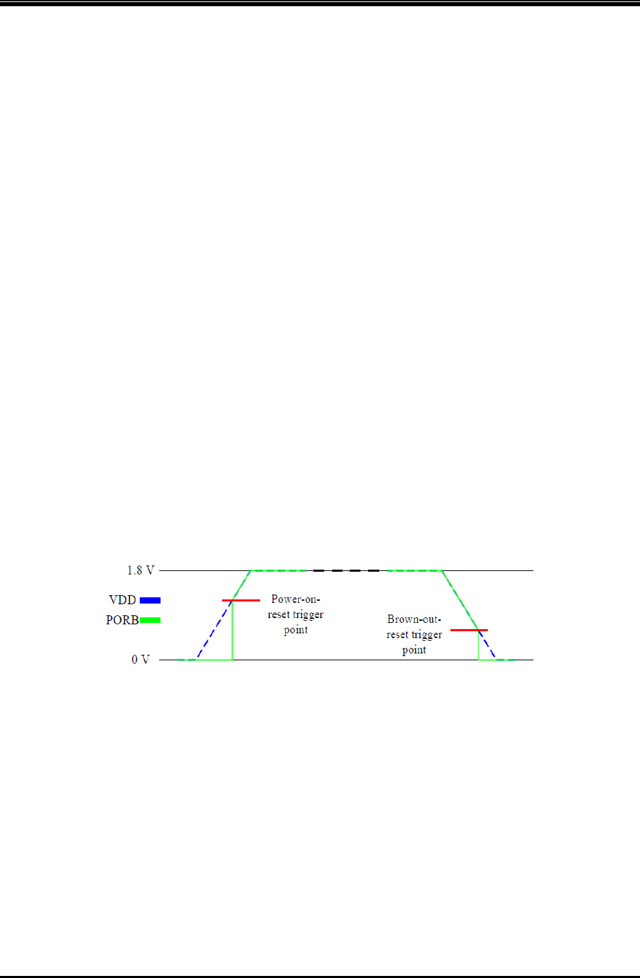
Figure 4-1 illustrates the power-on and reset signals waveform during proper power-on. Internally, there is TPOR
and TRC time for both the POR circuit and the internal counter. TPOR is the time for the POR circuit to stay at zero
voltage until it reaches VPOR and the time varies for different VDD rise-up time. It should be around 2/3 of the VDD
rise-up times. When the counter receives a high logic from the PORB signal, it is time for the internal counter to
count 4ms through the internal RC-oscillator, which is TRC. As a result, the overall internal reset time is the sum of
TPOR and TRC. Such a long time is required to ensure the Power is stable for system use. It also ensures all
internal logics are properly reset.
Figure 4-1 Power on reset
4.2 System Reset
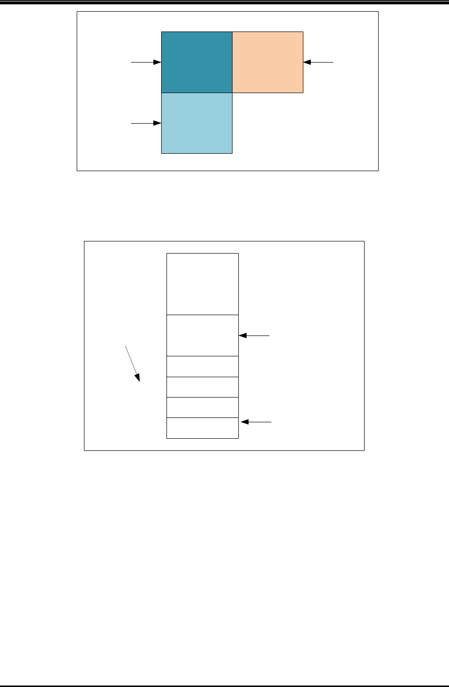
All reset signals are OR‟ed together inside the device to generate an overall system reset to reset the chip. Once
reset, the program memory address is reset to 8000h, which is the start address of the Normal Mode. Figure 4-2X
illustrates the reset sources.
26 4.2 System Reset
Version 1.0.0
Copyright ©2015, www.appotech.com. All Rights Reserved.
Watchdog reset
POR reset
LVD reset System Reset
OR
Port wakeup reset
RTCC reset
Figure 4-2 Reset Sources
4.2.1 LVD
CW6687B provides 4 levels programmable Low Voltage Detector (LVD) for user to detect VDDLDO power supply
voltage or external pin voltage multiplexed with GPIO P2.2. This is because VDDLDO is the input voltage source for
on-chip Low-Drop-Out regulator (LDO) which supplies power to internal VDDCORE. Hence, users can momentarily
monitor the VDDLDO power if it‟s externally connected to some batteries and for detection if the external power
source starts dropping to a level that CW6687B LDO can neither tolerate nor perform properly in the system
program.
LVD can also be used to monitor external voltage source through the GPIO P2.2 to enhance programmability for
different voltage levels. One example of this is it can be used to monitor external power sources or batteries voltage
or some voltages related to say pressure or temperature. It is there to provide a simple interface compared to ADC
since ADC requires more programming space and procedures to detect precise voltage level in detail. If the user
requires general voltage detection without fine voltage range, LVD will be a good choice compared to ADC
measurement. XTable 4-1X illustrates different voltage detection levels.
Remark:
When LVD_ENB is enabled, there is approximately 100us for the band-gap and the comparator to be stable
before the end-user can use it as low voltage detection. During the time, LVD_OEB has to be H in order to
disable the LVD output which possibly fluctuates signal level.
Different power supply falling times will affect the voltage detection. It is recommended that the power supply
falling time should be larger than 1ms for stable low voltage detection.
When detection occurs, interrupt can be generated if LVD interrupt is enabled, or, CW6687B can undergo reset if
interrupt is disabled.
Note that the detection is slightly dependent on power supply‟s falling rate and during power drop, noise fluctuation
may alter the detection results. For this reason, internally the comparator has about 150mV hysteresis voltage level
defined as VHYS = VLVDR-VLVDS to filter out any noise that may occur. Also, the detection level may have a
maximum of 100mV difference compared to the value stated in Table 4-1X
Table 4-1 LVD level setting
BORS[3:0] Detected VDDLDO V BORS[3:0] Detected VDDLDO V
4'b0000 2.200 4'b1000 3.267

4 Reset Generation 27
Version 1.0.0
Copyright ©2015, www.appotech.com. All Rights Reserved.
BORS[3:0] Detected VDDLDO V BORS[3:0] Detected VDDLDO V
4'b0001 2.333 4'b1001 3.400
4'b0010 2.467 4'b1010 3.533
4'b0011 2.600 4'b1011 3.667
4'b0100 2.733 4'b1100 3.800
4'b0101 2.867 4'b1101 3.933
4'b0110 3.000 4'b1110 4.067
4'b0111 3.133 4'b1111 4.200
For an ideal operation, it is recommended to perform the following for LVD.
1. Select either VDDLDO or external pin to be monitored. Set VD1_ENB = 0 for VDDLDO or VD2_ENB = 0 for
external pin
2. Select the detection voltage by setting bits BORS[3:0]
3. Enable the LVD by setting LVD_ENB = 0
4. Wait for at least 30us for the internal band-gap and comparator to become stable
5. Enable the LVD output by setting LVD_OEB = 0
6. The EX_PIN detect voltage must be less than VDDIO
Register 4-1 LVDCON– LVD control
Position 7 6 5 4 3 2 1 0
Name LVDIF LVDRSTEN LVDOE
Default 0 1 0 0 1 0 0 0
Access R/W R/W R/W R/W R/W R/W R/W R/W
LVDIF: LVD interrupt pending bit.
0 = When LVD threshold not detect. Cleared by writing a 0 to it
1 = When LVD threshold is detected
LVD_RSTEN: LVD Reset enable bit. Low active
0 = LVD Reset is disabled
1 = LVD is enabled
LVD_EN: LVD enable bit. Low active
0 = LVD is enabled
1 = LVD is disabled
LVD_OE: LVD output enable bit. Low active
0 = LVD output is enabled
1 = LVD output is disabled
VD2_EN: External pin (P0.0) voltage enable bit. Low active
0 = External pin voltage detection is enabled
1 = External pin voltage detection is disabled
VD1_EN: VDDLDO voltage enable bit. Low active
0 = VDDLDO voltage detection is enabled
1 = VDDLDO voltage detection is disabled

28 4.3 Clock System
Version 1.0.0
Copyright ©2015, www.appotech.com. All Rights Reserved.
LVDS: Voltage detection level select
00 = 2.2V/1.2V
01 = 2.4V/1.95V
10 = 2.7V/2.2V
11 = 3.1V/2.5V
4.2.2 RTCC Reset
CW6687B can be reset by RTCC second and alarm interrupt when IRTRSTEN bit in RTCON is set to 1.
4.2.3 Watchdog Reset
If Watchdog timer is enabled, and WDTCON [5] is not written by 1 within watchdog overflow time period, CW6687B
will be reset by Watchdog overflow.
4.2.4 Port Wakeup Reset
During SLEEP mode, port wakeup event will cause CW6687B to reset.
4.3 Clock System
4.3.1 Clock Control
CW6687B embeds 32K/4M/12M/24M OSC internal oscillator circuits. External crystal is needed to generate a clock
source. One internal PLL can generate 48MHz from the crystal clock source. One internal RC oscillator is also
embedded.
To make sure the USB module operates properly, the USB clock must be set to 48MHz. In this case, system clock
can be 48 MHz or 24MHz.
Register 4-2 PCON0 – Power control 0
Position 7 6 5 4 3 2 1 0
Name DRAMCEN IRAMCEN IROMCEN RAM2CEN IRCEN IDLE HOLD SLEEP
Default 0 0 0 0 0 0 0 0
Access R/W R/W R/W R/W R/W R/W R/W R/W
DRAMCEN: DECRAM clock enable
0 = Enable
1 = Disable
IRAMCEN: IRAM clock enable
0 = Enable
1 = Disable
IROMCEN: IROM clock enable
0 = Enable
1 = Disable

4 Reset Generation 29
Version 1.0.0
Copyright ©2015, www.appotech.com. All Rights Reserved.
RAM2CEN: RAM2 clock enable
0 = Enable
1 = Disable
IRCEN: IR clock enable
0 = Enable
1 = Disable
IDLE: IDLE mode
0 = Disable
1 = Enable IDLE mode
HOLD: HOLD mode
0 = Disable
1 = Enable HOLD mode
SLEEP: SLEEP mode
0 = Disable
1 = Enable SLEEP mode
Register 4-3 PCON1 – Power control 1
Position 7 6 5 4 3 2 1 0
Name DACCEN MP3CEN IISCEN TMRCEN UARTCEN SDCCEN FFTCEN SPICEN
Default 1 0 0 0 0 0 1 0
Access R/W R/W R/W R/W R/W R/W R/W R/W
DACCEN: DAC clock enable
0 = Enable
1 = Disable
MP3CEN: MP3 decoder clock enable
0 = Enable
1 = Disable
IISCEN: IIS clock enable
0 = Enable
1 = Disable
TMRCEN: Timer clock enable
0 = Enable
1 = Disable
UARTCEN: UART clock enable
0 = Enable
1 = Disable
SDCCEN: SDC clock enable
0 = Enable
1 = Disable
FFTCEN: FFT/IFFT clock enable

30 4.3 Clock System
Version 1.0.0
Copyright ©2015, www.appotech.com. All Rights Reserved.
0 = Enable
1 = Disable
SPICEN: SPI clock enable
0 = Enable
1 = Disable
Register 4-4 PCON2 – Power control 2
Position 7 6 5 4 3 2 1 0
Name IROM1CEN USBCEN TSCLK_OUT_EN EMICEN RTCCEN WDTCEN LVDCEN ADCCEN
Default 0 0 0 0 0 0 0 0
Access R/W R/W R/W R/W R/W R/W R/W R/W
IROM1CEN: IROM1 clock enable
0 = Enable
1 = Disable
USBCEN: USB clock enable
0 = Enable
1 = Disable
TSCLK_OUT_EN: RC or PLL clock output enables
0 = Disable
1 = Enable
EMICEN: EMI clock enable
0 = Enable
1 = Disable
RTCCEN: RTCC clock enable
0 = Enable
1 = Disable
WDTCEN: WDT clock enable
0 = Enable
1 = Disable
LVDCEN: LVD clock enable
0 = Enable
1 = Disable
ADCCEN: ADC clock enable
0 = Enable
1 = Disable
Register 4-5 PCON3 – Power control 3
Position 7 6 5 4 3 2 1 0
Name XOSC32KEN XOSC12MEN BASSCEN AUALUEN FMAMCEN AGCEN RCEN SYS_PLL_SEL
Default 0 0 1 1 1 1 1 0

4 Reset Generation 31
Version 1.0.0
Copyright ©2015, www.appotech.com. All Rights Reserved.
Access R/W R/W R/W R/W R/W R/W R/W R/W
XOSC32KEN: XOSC 32K enable
0 = Disable
1 = Enable
XOSC12MEN: XOSC 12M enable
0 = Disable
1 = Enable
BASSCEN: Bass clock enable
0 = Enable
1 = Disable
AUALUEN: Audio clock enable
0 = Disable
1 = Enable
FMAMCEN: FMAM clock enable
0 = Enable
1 = Disable
AGCEN: AGC clock enable
0 = Enable
1 = Disable
RCEN: RC enable bit
0 = Disable
1 = Enable
SYS_PLL_SEL: system PLL clock select
0 = PLL1 48MHz
1 = PLL2 49.152 MHz
Register 4-6 PCON4 – Power control 4
Position 7 6 5 4 3 2 1 0
Name BTPLL_EN BTRAMCEN MP3ECEN WMACEN APECEN AECRCEN AECCEN
Default 0 0 0 0 0 0 0 0
Access R/W R/W R/W R/W R/W R/W R/W R/W
BTPLL_EN: BT PLL enable
0 = Enable
1 = Disable
BTRAMCEN: BTRAM control clock enable
0 = Enable
1 = Disable
MP3ECEN: MP3 encoder clock enable
0 = Enable
1 = Disable

32 4.3 Clock System
Version 1.0.0
Copyright ©2015, www.appotech.com. All Rights Reserved.
WMACEN: WMA decoder clock enable
0 = Enable
1 = Disable
APECEN: APE decoder clock enable
0 = Enable
1 = Disable
AECRCEN: AEC ram clock enable
0 = Enable
1 = Disable
AECCEN: AEC clock enable
0 = Enable
1 = Disable
Register 4-7 PCON5 – Power control 5
Position 7 6 5 4 3 2 1 0
Name MP3_LP_EN VDDIOLDO_UNSNIFF SBUCKEN SWPD_EN PSWPD
Default 0 0 0 0 0 0 0 0
Access R/W R/W R/W R/W R/W R/W R/W R/W
MP3_LP_EN: MP3 enter low power
0 = exit low power mode
1 = enter low power mode
VDDIOLDO_UNSNIFF: VDDIO LDO unsniff enable
0 = Enable
1 = Disable
SBUCKEN: Sniff BUCK enable
0 = Enable
1 = Disable
SWPDEN: enable
0 = Enable
1 = Disable
PSWPD:
0 = Enable
1 = Disable
Register 4-8 PCON6 – Power control 6
Position 7 6 5 4 3 2 1 0
Name LPWK_TMRSEL
Default 0 0 0 0 0 0 0 0
Access R/W R/W R/W R/W R/W R/W R/W R/W
LPWK_TMR_SEL: low power wake up time seletion

4 Reset Generation 33
Version 1.0.0
Copyright ©2015, www.appotech.com. All Rights Reserved.
00 = 256 X system clock
01 =128 X system clock
10 = 16 X system clock
11 = 2 X system clock
1 = enter low power mode
Register 4-9 CLKCON – Clock control
Position 7 6 5 4 3 2 1 0
Name Reserved RCSEL WDTCSEL RTCCS SCSEL
Default 0 0 0 0 0 0 0 0
Access R/W R/W R/W R/W R/W R/W R/W R/W
RCSEL: RC frequency select
00 = RC 512K
01 = RC 32K
10 = RC 1M
11 = RC 4M or XOSC26M controlled by CLKCON2[3]
WDTCSEL: WDT clock section
0 = Internal 32 KHz RC oscillator output
1 = External 32 KHz or 12MHz crystal oscillator controlled by CLKCON2 [6] and CLKCON2 [7]
RTCCS: RTCC clock source select
00 = External 32 KHz or 12MHz crystal oscillator controlled by CLKCON2 [6] and CLKCON2 [7]
01 = Internal 32 KHz RC oscillator output
10 = Select 32 KHz clock source derived from external 12MHz crystal oscillator
11 = Reserve
SCSEL: System clock select
00 = Internal 512 KHz RC oscillator output
01 = External 32 KHz or 12MHz crystal oscillator controlled by PCON3 [5]
10 = PLL 48/24/16/12 MHz output, controlled by CLKCON1 [1:0]
11 = Reserve
Register 4-10 CLKCON1 – Clock control 1
Position 7 6 5 4 3 2 1 0
Name ATCLKSEL BTPLL_SEL DECDIV SYSDIV PLLDIVSEL
Default 0 0 0 0 0 0 0 0
Access R/W R/W R/W R/W R/W R/W R/W R/W
ATCLKSEL: Audio clock select
00 = Select external 12MHz crystal oscillator invert
01 = Select external 12MHz crystal oscillator
10 = Select PLL 24MHz output invert
11 = Select PLL 24MHz output

34 4.3 Clock System
Version 1.0.0
Copyright ©2015, www.appotech.com. All Rights Reserved.
BTPLL_SEL: BT PLL output 48M selection
0 = not select BT PLL
1 = Select BT PLL 48M as system PLL and DAC PLL
DECDIV: Decoder clock divide 2 from system clock
0 = Disable
1 = Enable
SYSDIV: System clock divide from clock source
00 = System clock source
01 = Divided by 2 from system clock source
10 = Divided by 4 from system clock source
11 = Divided by 8 from system clock source
PLLDIVSEL: PLL output divide select
00 = Select 48MHz output
01 = Select 24MHz output
10 = Select 16MHz output
11 = Select 12MHz output
Register 4-11 CLKCON2 – Clock control 2
Position 7 6 5 4 3 2 1 0
Name IISREFCSEL IISBCSEL TSCLK_OUT_SEL IR32K_SEL IR_CLK_SEL
Default 0 0 0 0 0 0 0 0
Access R/W R/W R/W R/W R/W R/W R/W R/W
IISREFCSEL: IIS Reference clock source select
00 = Select system clock
01 = Select XOSC12M
10 = Select PLL2
11 = Select PLL2 div2
IISBCSEL: IIS BCLK generate clock source select
00 = Select system clock
01 = Select external 12MHz crystal oscillator
01 = Select PLL2
11 = Select PLL2 div2
TSCLK_OUT_SEL: RC or PLL clock output select
0 = RC clock output
1 = 26MHz XOSC from BT
IR32K_SEL: IR digital model work at 32K clock
0 = Work at 1M clock
1 = Work at 32K clock
IR_CLK_SEL: ir_clk sel divide select

4 Reset Generation 35
Version 1.0.0
Copyright ©2015, www.appotech.com. All Rights Reserved.
00 = 1MHz PLL
01 = 1MHz RC
10 = External 32 KHz or 12MHz crystal oscillator controlled by CLKCON2 [6] and CLKCON2 [7] as shown in X
11 = 1MHz div form XOSC26M
4.3.2 Operation Guide
User guide 1:
CW6687B integrates a 4M RC clock called RC4M, extern OSC 26MHz, extern OSC 32K or 12MHz
4.3.3 Clock Gating
CW6687B provides comprehensive clock gating options for eliminating power-wasting activities. System clock
supplies clock signal to different clock domains. Every clock can be gated. It allows the user to shut down the clock
signal when the function is not needed.
4.3.4 Phase Lock Loop (PLL)
CW6687B provides one on-chip Phase Locked Loop (PLL 48M) clock generators. The PLL has a reference clock
from external 32 KHz/4M/12 M crystal oscillators to provide a stable reference clock, and the reference clock is
multiplied to provide the final PLL output.
Register 4-12 PLLCON – PLL Configuration
Position 7 6 5 4 3 2 1 0
Name SDADCLKEN PLLTCLKSEL SDADCCLK_SEL PLL12DREF_SEL PLL1 DREF_SEL
Default 0 0 0 0 0 0 0 0
Access R/W R/W R/W R/W R/W R/W R/W R/W
PLL1AREF_SEL: PLL1 input reference clock digital select
00 = XOSC
01 = RCOSC
10 = RCOSC div
11 = Reserved
PLL2AREF_SEL: PLL2 input reference clock digital select
00 = XOSC
01 = RCOSC
10 = PLL1 div
11 = Reserved
SDADCCLK_SEL: SDADC clockl select
00 = XOSC inv
01 = XOSC
10 = PLL2 div2 inv
11 = PLL2

36 4.3 Clock System
Version 1.0.0
Copyright ©2015, www.appotech.com. All Rights Reserved.
PLLTCLKSEL: PLL digital test clock select enable
0 = disable
1 = enable
SDADCEN: SDADC clock enable
0 = disable
1 = enable
Register 4-13 PLL1CON – PLL1 Configuration
Position 7 6 5 4 3 2 1 0
Name Reserved Reserved PLL1 AREF_SEL X12EN PLL1DEN32K PLL1DEN PLL1AEN
Default 0 0 0 0 0 0 0 0
Access R/W R/W R/W R/W R/W R/W R/W R/W
PLL1AEN: PLL analog module enables
0 = Disable
1 = Enable
PLL1DEN: PLL digital module enables
0 = Disable
1 = Enable
When change the divider, also need write 1 to PLLDEN
PLL1DEN32K: PLL digital 32K enable
0 = disable
1 = enable
X12EN: XOSC 12M 374 divider enable bit
0 = Disable
1 = Enable
PLL1AREF_SEL: PLL input reference clock analog select
00 = 12M XOSC
01 = 4M XOSC
10 = 32K XOSC
11 = 32K XOSC
Register 4-14 PLL1DIV – PLL1 clock div for PLL2
Position 7 6 5 4 3 2 1 0
Name PLL1DIV
Default 0 0 0 0 0 0 0 0
Access R/W R/W R/W R/W R/W R/W R/W R/W
PLL1IDV Clock = 48MH/PLL1DIV;
Register 4-15 PLL1INT – PLL1 integer low

4 Reset Generation 37
Version 1.0.0
Copyright ©2015, www.appotech.com. All Rights Reserved.
Position 7 6 5 4 3 2 1 0
Name PLL1INT
Default 0 0 1 0 0 1 1 1
Access R/W R/W R/W R/W R/W R/W R/W R/W
PLL1INT = int (60MHz/pll1_refclock)
Register 4-16 PLL1FRACH – PLL1 fraction high
Position 7 6 5 4 3 2 1 0
Name FRACH
Default 0 0 0 0 0 0 0 0
Access R/W R/W R/W R/W R/W R/W R/W R/W
Register 4-17 PLL1FRACL – PLL1 fraction low
Position 7 6 5 4 3 2 1 0
Name FRACL
Default 0 0 0 0 0 0 0 0
Access R/W R/W R/W R/W R/W R/W R/W R/W
When the fraction is less than 0.25, set FOVER to =1, and fraction = (fraction+1)/2, integer = (integer-1)
When the fraction is greater than 0.80, set FOVER to=1, and fraction = fraction/2, integer = integer
FRAC = fraction*65535;
Register 4-18 PLL2CON – PLL2 Configuration
Position 7 6 5 4 3 2 1 0
Name Reserved PLL2TSEL PLL2 AREF_SEL PLL1_DIVEN PLL2DEN32K PLL2DEN PLL2AEN
Default 0 0 1 0 0 1 0 0
Access R/W R/W R/W R/W R/W R/W R/W R/W
PLL2AEN: PLL2 analog module enables
0 = Disable
1 = Enable
PLL2DEN: PLL2 digital module enables
0 = Disable
1 = Enable
When change the divider, also need write 1 to PLL2DEN
PLL2DEN32K: PLL2 digital 32K enable
0 = disable
1 = enable
PLL1_DIVEN: PLL1 divide enable
0 = disable
1 = enable

38 4.3 Clock System
Version 1.0.0
Copyright ©2015, www.appotech.com. All Rights Reserved.
PLL2AREF_SEL: PLL2 input reference clock analog select
00 = 12M XOSC
01 = 4M XOSC
10 = 32K XOSC
11 = 32K XOSC
PLL2TSEL: PLL2 test select
0 = PLL2 refclock output
1 = PLL2 fbclock output
Register 4-19 PLL2INTH – PLL2 integer high
Position 7 6 5 4 3 2 1 0
Name PLL2INT[11:8]
Default 0 0 0 0 1 0 1 1
Access R/W R/W R/W R/W R/W R/W R/W R/W
Register 4-20 PLL2INTL – PLL2 integer low
Position 7 6 5 4 3 2 1 0
Name PLL2INT[7:0]
Default 1 0 1 0 1 0 0 0
Access R/W R/W R/W R/W R/W R/W R/W R/W
PLL2INT = int(98.304MHz/pll2_refclock)
Register 4-21 PLL2FRACH – PLL2 fraction high
Position 7 6 5 4 3 2 1 0
Name FRACH
Default 0 0 0 0 0 0 0 0
Access R/W R/W R/W R/W R/W R/W R/W R/W
Register 4-22 PLL2FRACL – PLL2 fraction low
Position 7 6 5 4 3 2 1 0
Name FRACL
Default 0 0 0 0 0 0 0 0
Access R/W R/W R/W R/W R/W R/W R/W R/W
When the fraction is less than 0.25, set FOVER=1, and fraction = (fraction+1)/2, integer = (integer-1)
When the fraction is more than 0.80, set FOVER=1, and fraction = fraction/2, integer = integer
FRAC = fraction*65535
User’s guide:
1. PLL1 frequency division
a) PLL1‟s:
-input reference clock is f0 (from RC or OSC)

4 Reset Generation 39
Version 1.0.0
Copyright ©2015, www.appotech.com. All Rights Reserved.
-internal dividing clock is 60M
-frequency dividing ratio is 60M/f0.
b)
Clock divide ratio consists of integer and decimal
-default value of integer part is 1831(default reference clock is 32.768k)
-default value of decimal part is 0(only integral frequency division this time).
c)
If f0=32.768k, frequency dividing ratio is 1831, decimal fraction part set 0.
If f0=12M, frequency dividing ratio is 5, decimal fraction part set 0.
If f0=4M, frequency dividing ratio is 15, decimal fraction part set 0.
2. If frequency dividing ratio is 58.a, then integer set 58, decimal fraction is a*65535.
3. PLL2 same as PLL1

40 5.1 Power Saving Mode
Version 1.0.0
Copyright ©2015, www.appotech.com. All Rights Reserved.
5 Low Power Management
5.1 Power Saving Mode
CW6687B device offers low power management mode that helps reduce power consumption when the device does
not require intensive CPU resources and speed. There are four low power modes available: SLEEP mode, Hold
mode, IDLE mode and power down mode.
5.1.1 Sleep Mode
SLEEP mode is an ultimate power reduction mode that will stop all the clock sources, and all the memory chip select
signals are disabled to further reduce power consumption. However, before entering sleep mode, all peripherals
should be disabled separately, especially those analog peripherals and memory, unless those peripherals will stop
themselves if no clock source is applied to the peripherals.
Note: Before Entering SLEEP mode, the system clock is recommended to change back to oscillator clock as the
system clock.
To enter SLEEP mode, the user needs to write a „1‟ to SLEEP register (Bit0 of PCON0).
During SLEEP mode, the device can perform wake up by external port wakeup reset, watchdog reset or RTCC
reset.
After exit SLEEP mode by wakeup, the device will be reset.
SLEEP mode will enable DECRAM, and IRAM and system clock automatically.
5.1.2 Hold Mode
HOLD mode will stop the clock from entering the system. The system clock is gated with the HOLD mode control.
Once enter HOLD mode, clock to the system logic halts. Therefore, there will be no clock switching entering the
system logic, minimizing power usage due to the absence of AC switching. However, the clock sources are not
disabled and they are still running. This allows the clock to be resumed in real time without waiting for the PLL to lock
again. Watchdog interrupt, RTCC interrupt, Port interrupt and all reset event will cause system to exit HOLD mode.
TO enter HOLD mode, the user needs to write a „1‟ to HOLD register (Bit1 of PCON0).
During wakeup from HOLD Mode by port or RTCC with interrupt enabled, CW6687B enters corresponding interrupt
service subroutine (ISR), else CW6687B will execute the instruction following HOLD.
During wakeup from HOLD Mode by watchdog with watchdog reset enabled, CW6687B will be reset, else if
watchdog interrupt is enabled, CW6687B will enter watchdog‟s ISR. Otherwise, CW6687B will execute the
instruction following HOLD.
5.1.3 Idle Mode
IDLE mode will stop the clock from entering to the CPU. The CPU clock is gated with the IDLE mode control. Once
you enter IDLE mode, the clock to the CPU logic will stop. Therefore, there will be no clock switching entering the
CPU logic so CPU power consumption is minimized.
All interrupt sources will cause system to exit IDLE mode, which includes all peripheral interrupt.
TO enter IDLE mode, user need to write a „1‟ to IDLE register (Bit2 of PCON0).

5 Low Power Management 41
Version 1.0.0
Copyright ©2015, www.appotech.com. All Rights Reserved.
Upon exiting IDLE mode, CW6687B will enter interrupt service subroutine if EA is enabled. If EA is disabled, the
instruction next to IDLE will be executed.
5.1.4 Power Down Mode
Power Down mode will disable core 1.2V and VDDIO 3.3V power, so all the IO state, RAM, OTP, MROM and logic
(except for IRTCC) will be powered off. The content in RAM and logic disappears, should be initial after wake up.
Enter power down mode:
1) Disable the entire analog model
2) Select wake up source in WK_EN
3) Disable RC, RVDD, VDD1P8, VDD3P3, PMU, in PWRCON (RTC power field); RCEN, RVDD_EN, DVDD_EN,
VDDIO_EN, PMU_EN
Power down mode wake up source:
1) RTC alarm wake up
2) RTC WKO pin wake up
3) RTC every minute wake up
4) RTC every day wake up
NOTE: After exit Power Down mode by wakeup, the device will be reset.
5.2 Power Supply
CW6687B provides two on-chip low drop-out regulators (LDO) to convert from 5V to 3.3V, 1.5V to 1.2V for internal
core power use. It is there to provide high power supply noise rejection and also to minimize power consumption.
LDO is always enabled.
CW6687B also provides Build-in buck converter, DC-DC 5V to 1.5V
To provide a more stable and reliable power source for internal core logic, add frequency compensation through
external component. XFigure 5-1 shows the connection.
BUCK
DC_DC
BVIN1/BVIN1P
VOUT2V1
EN
LX
DRREG_EN
VDD
VSS
BVSS1/BVSS1P
DRPD
VSSIO
BVSS1
RREG
DREG
VOUT2V1
RVDD
VDDCORE
VOUT2V1
VDDIO
LDO
VBAT
VDDIO
VDDRTC
BG
LVD
VDDRTC
VBAT VDDRTC
VDDIO VDD
VDDIO
C1
C0
C2 C3
L0
Figure 5-1 Frequency compensation through external component

42 5.2 Power Supply
Version 1.0.0
Copyright ©2015, www.appotech.com. All Rights Reserved.
Note:
The recommended value for L0 is 10 uH.
The recommended value for C0 is 10 uF.
The recommended value for C1 is 10 uF.
The recommended value for C2 is 10 uF.
The recommended value for C3 is 10 uF.
L0, Cx should be placed closely to the chip.
LDO enable and current select configure, please refer to “Register 5-x PWRCONx – Power control”
Register 5-1 PWRCON1 – Power control 1
Position 7 6 5 4 3 2 1 0
Name DB1MODE1 DB1MODE0 DB1TB2 DB1TB1 DB1TB0 DZISEL2 DZISEL1 DZISEL0
Default 0 1 0 0 0 0 0 0
Access R/W R/W R/W R/W R/W R/W R/W R/W
DB1MODE1~0:BUCK mode choose
00 = force PFM mode
01 = force PWM mode
10 = ---
11 = ---
DB1TB2~0:BUCK output voltage fine tune
DZISEL2~0:ZERO_de current adjust
Register 5-2 PWRCON2 – Power control 2
Position 7 6 5 4 3 2 1 0
Name BORS3 BORS2 BORS1 BORS0 - DPR_AD1 DPR_AD0 DRINGOFF
Default 0 0 0 0 - 0 0 0
Access RW RW RW RW - RW RW RW
DRINGOFF:
DPR_AD1~DPR_AD0:PWM regulator voltage select:
00 = 1.2V
01 = 1.6V
10 = 1.8V
11 = 2.1V
BORS3~BORS0:VDDLDO detection voltage selection(VLVDR/VLVDS V).
S=0000 : 2.26/2.41
S=0001 : 2.39/2.54
S=0010 : 2.54/2.68
S=0011 : 2.66/2.81
S=0100 : 2.79/2.96
S=0101 : 2.92/3.11
S=0110 : 3.06/3.24

5 Low Power Management 43
Version 1.0.0
Copyright ©2015, www.appotech.com. All Rights Reserved.
S=0111 : 3.19/3.39
S=1000 : 3.32/3.53
S=1001 : 3.345/3.68
S=1010 : 3.59/3.81
S=1011 : 3.72/3.96
S=1100 : 3.85/4.1
S=1101 : 4.0/4.25
S=1110 : 4.14/4.38
S=1111 : 4.21/4.47
Register 5-3 PWRCON3 – Power control 3
Position 7 6 5 4 3 2 1 0
Name V33SEL1 V33SEL0 LVD_OEB LVD_EN BGOPEN BATDET
Default 1 0 0 1 0 0
Access RW RW RW RW RW RW
BATDET:Battery voltage detection enable
1=enable
0=disable
BGOPEN:Bg voltage output enable
1=enable
0=disable
LVD_EN:LVD module enable
1=enable
0=disable
LVD_OEB:LVD output enable
1=enable
0=disable
V33SEL1~ V33SEL0:VDDIO voltage selection
00 = 2.8V
01 = 2.9V
10 = 3.0V
11 = 3.3V
Register 5-4 PWRCON4 – Power control 4
Position 7 6 5 4 3 2 1 0
Name CURRENTSEL_D1 CURRENTSEL_D0 V18SELR1 V18SELR0 CURRENTSEL_R1 CURRENTSEL_R0 VD2_ENB VD1_ENB
Default 1 0 1 0 1 0 1 0
Access RW RW RW RW RW RW RW RW
VD1_ENB:VDDLDO voltage detection enable
0=enable

44 5.2 Power Supply
Version 1.0.0
Copyright ©2015, www.appotech.com. All Rights Reserved.
1=disable
VD2_ENB:External pin voltage detection enable.
0=enable
1=disable
CURRENTSEL_R1~CURRENTSEL_R0:Modulate 3.3v LDO sleep current
V18SELR1~ V18SELR0:RF part LDO output voltage selection:
00 = 1.15
01 = 1.23
10 = 1.28 default
11 = 1.32
CURRENTSEL_D1~CURRENTSEL_D0:VDD core LDO amp bias current selection
00 = X1
01 = X2
10 = X3 default
11 = X4
Register 5-5 PWRCON5 – Power control 5
Position 7 6 5 4 3 2 1 0
Name SBG_TRM VSEL1_LV VSEL0_LV V18SELD1 V18SELD0
Default
Access RW RW RW RW RW RW RW RW
SBG_TRM:BG voltage adjust
VSEL1_LV~ VSEL0_LV:VDDCORE Output voltage of sniff mode select
00 = 1.2V
01 = 0.8V
10 = 0.9V
11 = 1.0V
V18SELD1~ V18SELD0:VDD core part LDO output voltage selection
00 = 1.15
01 = 1.23
10 = 1.28 default
11 = 1.32
Register 5-6 CHAGCON0 – charger control 0
Position 7 6 5 4 3 2 1 0
Name CH_TERM CH_TERM_EN ITERM_SEL BG_TR
Default 0 0 0 1 0 1 1 1
Access RW RW RW RW RW RW RW RW
CH_TERM:Software stop charge enable

5 Low Power Management 45
Version 1.0.0
Copyright ©2015, www.appotech.com. All Rights Reserved.
0 = disable
1 = enable
CH_TERM_EN:Software stop charge enable
0 = charge hardware stop
1 = software control stop charge
ITERM_SEL:Stop charge current selection
00 =20mA;
01 =40mA;
10 =60mA;
11-80mA
BG_TR:BG trimming bit, every step is 0.8%
0000 = Min
1111 = Max
Register 5-7 CHAGCON1 – charger control 1
Position 7 6 5 4 3 2 1 0
Name DCIN_DET CHAG_VPND CHAG_IPND EN_BG_BUF CUR_TR
Default 0 0 0 0 0 0 0
Access RW RW RW RW RW RW RW RW
DCIN_DET:DC insert detect
0 = No dc insert
1 = DC insert
CHAG_VPND:Charger voltages reach 4.1V pending
0 = Charging
1 = Finish
CHAG_IPND:Charger current reach the current that configuration
0 = Charging
1 = Finish

46 6.1 Overview
Version 1.0.0
Copyright ©2015, www.appotech.com. All Rights Reserved.
6 General Purpose Input/Output (GPIO)
6.1 Overview
The general-purpose input/output port (GPIO) provides 30 dedicated general purpose one-bit contacts that can be
individually configured as either inputs or outputs. Contacts configured as outputs reflect internal register values,
and those configured as inputs can be detected by reading internal registers. All GPIOs are divided into5 groups:
Port0, Port1, Port2, Port3 and Port4.
6.2 Features
The GPIO includes the following features:
Drive specific data to output using the data register;
Control the direction of the signal using the GPIO direction register;
Enable CPU to sample the status of the corresponding inputs by reading the data register;
Enable internal pull-up resistor using pull-up resistor control register;
Select suitable pull-up resistor value;
Enable internal pull-up resistor using pull-down resistor control register;
Select suitable pull-down resistor value;
Select suitable output driving current capability;
There are 5 types of GPIO that can meet the variation of application requirements. Table 6-1 shows the difference
between pad types
Table 6-1 Pad types
Type Driving (mA) Pull-up resistor (Kohm) Pull-down resistor (Kohm) Mode
A 8 24 10 / / 10 / / / Normal
B 8 24 10 0.2 / 10 0.2 / / Normal
C 8 24 10 200 0.5 10 3.3 0.5 / Normal
D 8 24 10 / / 10 / / / MUTE
E / / / / / / / / / Analog
6.3 Function multiplexing
In order to provide more flexible port functions and to minimize pin counts, some of the ports are multiplexed with
other peripherals or functions. Table 6-2 illustrates the “Ports multiplexed mapping”.
Several GPIO are multiplexed with analog module. GPIO digital input and output must be disabled when the
corresponding analog module is enabled.
Table 6-2 Ports multiplexed mapping
Pins Func1 Func 2 Func3 Func4 Func5 Func6 Func7 Fun8 Type

6 General Purpose Input/Output (GPIO) 47
Version 1.0.0
Copyright ©2015, www.appotech.com. All Rights Reserved.
Pins Func1 Func 2 Func3 Func4 Func5 Func6 Func7 Fun8 Type
P00 AUXL0 UARTRX1 SDDAT1 SPI0DIN2 A
P01 AUXR0 UARTTX1 PORTINT/WKUP0 SDDAT2 A
P02 AUXL1 SPI0DOUT1 TMR1PWM A
P03 AUXR1 SPI0CLK1 TMR0CAP A
P04 SPI1DOUT/DIN1 A
P05 SPI1CLK A
P06 PORTINT/WKUP1 SPI1DIN/SPI0DIN1 TMR0CKI/TMR1CKI IISDI0 A
P07 PORTINT/WKUP3 Ir_input TRM1CAP A
P10 EMIWR C
P11 C
P12 C
P13 ADC5 IISBCLK0 B
P14 ADC2 SDDAT3 SPI0DOUT2 TMR3CAP/TMR3PWM IISDO0 A
P15 TMR3CKI B
P16 BTUART1TX UARTTX0 Ir_input TMR2CAP/TMR2PWM IISREF A
P17 BTUART1RX TMR2CKI IISWS0 B
P20 AUXL2 SDCMD EMIDAT0 C
P21 AUXR2/ADC1 SDCLK EMIDAT1 C
P22 ADC3/LVDIN EMIDAT2 IISDO1 C
P23 EMIDAT3 IISDI1 C
P24 EMIDAT4 C
P25 EMIDAT5 SPI0DIN0/DOUT0 IISBCLK1 C
P26 ADC6 EMIDAT6 SPI0CLK0 IISWS1 C
P27 SDDAT0 EMIDAT7 SPI0DOUT0 C
P30 ADC4 SDCLK SPI0CLK3 C
P31 SDCMD SPI0DIN3 C
P32 SDDAT0 SPI0DOUT3/DIN3 C
P33 ADC0 Ir_input 32K/xosc12m SysClk TRM1CAP A
P34 UARTRX0 PORTINT/WKUP2 SPI0CLK2 TMR0PWM C
P35 MUTE D
P36 A
P37 GPIO B
P40 Ir_input SPI0CLK4 A
P41 A
P42 SPI1DIN1' A
P43 A
P44 DACL E
P45 DACR E

48 6.4 GPIO Special Function Registers
Version 1.0.0
Copyright ©2015, www.appotech.com. All Rights Reserved.
6.4 GPIO Special Function Registers
Register 6-1 P0DIR-P0 direction Register
Position 7 6 5 4 3 2 1 0
Name P0DIR
Default 1 1 1 1 1 1 1 1
Access R/W R/W R/W R/W R/W R/W R/W R/W
P0xDIR: P0x direction control
0 = Output
1 = Input
Register 6-2 P1DIR-P1 direction Register
Position 7 6 5 4 3 2 1 0
Name P1DIR
Default 1 1 1 1 1 1 1 1
Access R/W R/W R/W R/W R/W R/W R/W R/W
P1xDIR: P1x direction control
0 = Output
1 = Input
Register 6-3 P2DIR-P2 direction Register
Position 7 6 5 4 3 2 1 0
Name P2DIR
Default 1 1 1 1 1 1 1 1
Access R/W R/W R/W R/W R/W R/W R/W R/W
P2xDIR: P2x direction control
0 = Output
1 = Input
Register 6-4 P3DIR-P3 direction Register
Position 7 6 5 4 3 2 1 0
Name P3DIR
Default 1 1 1 1 1 1 1 1
Access R/W R/W R/W R/W R/W R/W R/W R/W
P3xDIR: P3x direction control
0 = Output
1 = Input
Register 6-5 P4DIR-P4 direction Register
Position 7 6 5 4 3 2 1 0
Name P4DIR

6 General Purpose Input/Output (GPIO) 49
Version 1.0.0
Copyright ©2015, www.appotech.com. All Rights Reserved.
Default - - 1 1 1 1 1 1
Access - - R/W R/W R/W R/W R/W R/W
P4xDIR: P4x direction control
0 = Output
1 = Input
Register 6-6 P0 – P0 data register
Position 7 6 5 4 3 2 1 0
Name P0
Default x x x x x x x x
Access R/W R/W R/W R/W R/W R/W R/W R/W
P0[x]: P0x data. Valid when P0x is used as GPIO
0 = P0x is in low state when read and output low at P0x when write
1 = P0x is in high state when read and output high at P0x when write
Register 6-7 P1 – P1 data register
Position 7 6 5 4 3 2 1 0
Name P1
Default x x x x x x x x
Access R/W R/W R/W R/W R/W R/W R/W R/W
P1[x]: P1x data. Valid when P1x is used as GPIO
0 = P1x is in low state when read and output low at P1x when write
1 = P1x is in high state when read and output high at P1x when write
Register 6-8 P2 – P2 data register
Position 7 6 5 4 3 2 1 0
Name P2
Default x x x x x x x x
Access W/R W/R W/R W/R W/R W/R W/R W/R
P2[x]: P2x data. Valid when P2x is used as GPIO
0 = P2x is in low state when read and output low at P2x when write
1 = P2x is in high state when read and output high at P2x when write
Register 6-9 P3 – P3 data register
Position 7 6 5 4 3 2 1 0
Name P3
Default x x x x x x x x
Access W/R W/R W/R W/R W/R W/R W/R W/R
P3[x]: P3x data. Valid when P3x is used as GPIO
0 = P3x is in low state when read and output low at P3x when write
1 = P3x is in high state when read and output high at P3x when write
50 6.4 GPIO Special Function Registers
Version 1.0.0
Copyright ©2015, www.appotech.com. All Rights Reserved.
Register 6-10 P4 – P4 data register
Position 7 6 5 4 3 2 1 0
Name P4
Default - - x x x x x x
Access - - RO RO W/R W/R W/R W/R
P3[x]: P3x data. Valid when P3x is used as GPIO
0 = P3x is in low state when read and output low at P3x when write
1 = P3x is in high state when read and output high at P3x when write
Table 6-3 DRVx register setting
Register Address Set bit “x” of PxDRV0 as “1” Clear bit “x” of PxDRV0 as “0” Initial value
P0DRV0 R/W Driving is 24mA Driving is 8mA 00h
P1DRV0 R/W Driving is 24mA Driving is 8mA 00h
P2DRV0 R/W Driving is 24mA Driving is 8mA 00h
P3DRV0 R/W Driving is 24mA Driving is 8mA 00h
P4DRV0 R/W Driving Driving is 8mA 00h
Table 6-4 PUPx register setting
Register Address Set bit “x” of PxPU0 as “1” Clear bit “x” of PxPU0 as “0” Initial value
P0PU0 R/W Enable pull-up Disable pull-up 00h
P1PU0 R/W Enable pull-up Disable pull-up 00h
P2PU0 R/W Enable pull-up Disable pull-up 00h
P3PU0 R/W Enable pull-up Disable pull-up 00h
P4PU0 R/W Enable pull-up Disable pull-up 00h
Table 6-5 PDNx register setting
Register Address Set bit “x” of PxPD0 as “1” Clear bit “x” of PxPD0 as “0” Initial value
P0PD0 R/W Enable pull-down Disable pull-down 00h
P1PD0 R/W Enable pull-down Disable pull-down 00h
P2PD0 R/W Enable pull-down Disable pull-down 00h
P3PD0 R/W Enable pull-down Disable pull-down 00h
P4PD0 R/W Enable pull-down Disable pull-down 00h
Register 6–11 P1PUS0– P1 pull up select
Position 7 6 5 4 3 2 1 0
Name P17PUS0 P16PUS0 P15PUS0 P14PUS0 P13PUS0 P12PUS0 P11PUS0 P10PUS0
Default 0 0 0 0 0 0 0 0
Access W/R W/R W/R W/R W/R W/R W/R W/R
Register 6–12 P1PUS1– P1 pull up select
Position 7 6 5 4 3 2 1 0

6 General Purpose Input/Output (GPIO) 51
Version 1.0.0
Copyright ©2015, www.appotech.com. All Rights Reserved.
Name P17PUS1 P16PUS1 P15PUS1 P14PUS1 P13PUS1 P12PUS1 P11PUS1 P10PUS1
Default 0 0 0 0 0 0 0 0
Access W/R W/R W/R W/R W/R W/R W/R W/R
P17PUS1, P17PUS0:
00 = select 10K pull up
01 = select 200Ωpull up
1x = reverse
P16PUS1, P16PUS0:
00 = select 10K pull up
01 = select 500Ωpull up
1x = select 200K pull up
P15PUS1, P15PUS0:
00 = select 10K pull up
01 = select 200Ωpull up
1x = reverse
P14PUS1, P14PUS0:
00 = select 10K pull up
01 = reverse
1x = reverse
P13PUS1, P13PUS0:
00 = select 10K pull up
01 = reverse
1x = reverse
P12PUS1, P12PUS0:
00 = select 10K pull up
01 = select 500Ωpull up
1x = select 200K pull up
P11PUS1, P11PUS0:
00 = select 10K pull up
01 = select 500Ωpull up
1x = select 200K pull up
P10PUS1, P10PUS0:
00 = select 10K pull up
01 = select 500Ωpull up
1x = select 200K pull up

52 6.4 GPIO Special Function Registers
Version 1.0.0
Copyright ©2015, www.appotech.com. All Rights Reserved.
Register 6–13 P2PUS0– P2 pull up select
Position 7 6 5 4 3 2 1 0
Name P27PUS0 P26PUS0 P25PUS0 P24PUS0 P23PUS0 P22PUS0 P21PUS0 P20PUS0
Default 0 0 0 0 0 0 0 0
Access W/R W/R W/R W/R W/R W/R W/R W/R
Register 6–14 P2PUS1– P2 pull up select
Position 7 6 5 4 3 2 1 0
Name P27PUS1 P26PUS1 P25PUS1 P24PUS1 P23PUS1 P22PUS1 P21PUS1 P20PUS1
Default 0 0 0 0 0 0 0 0
Access W/R W/R W/R W/R W/R W/R W/R W/R
P27PUS1, P27PUS0:
00 = select 10K pull up
01 = select 500Ωpull up
1x = select 200K pull up
P26PUS1, P26PUS0:
00 = select 10K pull up
01 = select 500Ωpull up
1x = select 200K pull up
P25PUS1, P25PUS0:
00 = select 10K pull up
01 = select 500Ωpull up
1x = select 200K pull up
P24PUS1, P24PUS0:
00 = select 10K pull up
01 = select 500Ωpull up
1x = select 200K pull up
P23PUS1, P23PUS0:
00 = select 10K pull up
01 = select 500Ωpull up
1x = select 200K pull up
P22PUS1, P22PUS0:
00 = select 10K pull up
01 = select 500Ωpull up
1x = select 200K pull up
P21PUS1, P21PUS0:
00 = select 10K pull up

6 General Purpose Input/Output (GPIO) 53
Version 1.0.0
Copyright ©2015, www.appotech.com. All Rights Reserved.
01 = select 500Ωpull up
1x = select 200K pull up
P20PUS1, P20PUS0:
00 = select 10K pull up
01 = select 500Ωpull up
1x = select 200K pull up
Register 6–15 P3PUS0– P3 pull up select
Position 7 6 5 4 3 2 1 0
Name P37PUS0 P36PUS0 P35PUS0 P34PUS0 P33PUS0 P32PUS0 P31PUS0 P30PUS0
Default 0 0 0 0 0 0 0 0
Access W/R W/R W/R W/R W/R W/R W/R W/R
Register 6–16 P3PUS1– P3 pull up select
Position 7 6 5 4 3 2 1 0
Name P37PUS1 P36PUS1 P35PUS1 P34PUS1 P33PUS1 P32PUS1 P31PUS1 P30PUS1
Default 0 0 0 0 0 0 0 0
Access W/R W/R W/R W/R W/R W/R W/R W/R
P37PUS1, P37PUS0:
00 = select 10K pull up
01 = select 200Ωpull up
1x = reverse
P36PUS1, P36PUS0:
00 = select 10K pull up
01 = reverse
1x = reverse
P35PUS1, P35PUS0:
00 = select 10K pull up
01 = reverse
1x = reverse
P34PUS1, P34PUS0:
00 = select 10K pull up
01 = select 500Ωpull up
1x = select 200K pull up
P33PUS1, P33PUS0:
00 = select 10K pull up
01 = reverse

54 6.4 GPIO Special Function Registers
Version 1.0.0
Copyright ©2015, www.appotech.com. All Rights Reserved.
1x = reverse
P32PUS1, P32PUS0:
00 = select 10K pull up
01 = select 500Ωpull up
1x = select 200K pull up
P31PUS1, P31PUS0:
00 = select 10K pull up
01 = select 500Ωpull up
1x = select 200K pull up
P30PUS1, P30PUS0:
00 = select 10K pull up
01 = select 500Ωpull up
1x = select 200K pull up
Register 6–17 P1PDS0– P1 pull down select
Position 7 6 5 4 3 2 1 0
Name P17PDS0 P16PDS0 P15PDS0 P14PDS0 P13PDS0 P12PDS0 P11PDS0 P10PDS0
Default 0 0 0 0 0 0 0 0
Access W/R W/R W/R W/R W/R W/R W/R W/R
Register 6–18 P1PDS1– P1 pull down select
Position 7 6 5 4 3 2 1 0
Name P17PDS1 P16PDS1 P15PDS1 P14PDS1 P13PDS1 P12PDS1 P11PDS1 P10PDS1
Default 0 0 0 0 0 0 0 0
Access W/R W/R W/R W/R W/R W/R W/R W/R
P17PDS1, P17PDS0:
00 = select 10K pull down
01 = select 200Ωpull down
1x = reverse
P16PDS1, P16PDS0:
00 = select 10K pull down
01 = select 500Ωpull down
1x = select 330Ωpull down
P15PDS1, P15PDS0:
00 = select 10K pull down
01 = select 200Ωpull down
1x = reverse

6 General Purpose Input/Output (GPIO) 55
Version 1.0.0
Copyright ©2015, www.appotech.com. All Rights Reserved.
P14PDS1, P14PDS0:
00 = select 10K pull down
01 = reverse
1x = reverse
P13PDS1, P13PDS0:
00 = select 10K pull down
01 = reverse
1x = reverse
P12PDS1, P12PDS0:
00 = select 10K pull down
01 = select 500Ωpull down
1x = select 330Ωpull down
P11PDS1, P11PDS0:
00 = select 10K pull down
01 = select 500Ωpull down
1x = select 330Ωpull down
P10PDS1, P10PDS0:
00 = select 10K pull down
01 = select 500Ωpull down
1x = select 330Ωpull down
Register 6–19 P2PDS0– P2 pull down select
Position 7 6 5 4 3 2 1 0
Name P27PDS0 P26PDS0 P25PDS0 P24PDS0 P23PDS0 P22PDS0 P21PDS0 P20PDS0
Default 0 0 0 0 0 0 0 0
Access W/R W/R W/R W/R W/R W/R W/R W/R
Register 6–20 P2PDS1– P2 pull down select
Position 7 6 5 4 3 2 1 0
Name P27PDS1 P26PDS1 P25PDS1 P24PDS1 P23PDS1 P22PDS1 P21PDS1 P20PDS1
Default 0 0 0 0 0 0 0 0
Access W/R W/R W/R W/R W/R W/R W/R W/R
P27PDS1, P27PDS0:
00 = select 10K pull down
01 = select 500Ωpull down
1x = select 330Ωpull down
P26PDS1, P26PDS0:

56 6.4 GPIO Special Function Registers
Version 1.0.0
Copyright ©2015, www.appotech.com. All Rights Reserved.
00 = select 10K pull down
01 = select 500Ωpull down
1x = select 330Ωpull down
P25PDS1, P25PDS0:
00 = select 10K pull down
01 = select 500Ωpull down
1x = select 330Ωpull down
P24PDS1, P24PDS0:
00 = select 10K pull down
01 = select 500Ωpull down
1x = select 330Ωpull down
P23PDS1, P23PDS0:
00 = select 10K pull down
01 = select 500Ωpull down
1x = select 330Ωpull down
P22PDS1, P22PDS0:
00 = select 10K pull down
01 = select 500Ωpull down
1x = select 330Ωpull down
P21PDS1, P21PDS0:
00 = select 10K pull down
01 = select 500Ωpull down
1x = select 330Ωpull down
P20PDS1, P20PDS0:
00 = select 10K pull down
01 = select 500Ωpull down
1x = select 330Ωpull down
Register 6–21 P3PDS0– P3 pull down select
Position 7 6 5 4 3 2 1 0
Name P37PDS0 P36PDS0 P35PDS0 P34PDS0 P33PDS0 P32PDS0 P31PDS0 P30PDS0
Default 0 0 0 0 0 0 0 0
Access W/R W/R W/R W/R W/R W/R W/R W/R
Register 6–22 P3PDS1– P3 pull down select
Position 7 6 5 4 3 2 1 0
Name P37PDS1 P36PDS1 P35PDS1 P34PDS1 P33PDS1 P32PDS1 P31PDS1 P30PDS1

6 General Purpose Input/Output (GPIO) 57
Version 1.0.0
Copyright ©2015, www.appotech.com. All Rights Reserved.
Default 0 0 0 0 0 0 0 0
Access W/R W/R W/R W/R W/R W/R W/R W/R
P37PDS1, P37PDS0:
00 = select 10K pull down
01 = select 200Ωpull down
1x = reverse
P36PDS1, P36PDS0:
00 = select 10K pull down
01 = reverse
1x = reverse
P35PDS1, P35PDS0:
00 = select 10K pull down
01 = reverse
1x = reverse
P34PDS1, P34PDS0:
00 = select 10K pull down
01 = select 500Ωpull down
1x = select 330Ωpull down
P33PDS1, P33PDS0:
00 = select 10K pull down
01 = reverse
1x = reverse
P32PDS1, P32PDS0:
00 = select 10K pull down
01 = select 500Ωpull down
1x = select 330Ωpull down
P31PDS1, P31PDS0:
00 = select 10K pull down
01 = select 500Ωpull down
1x = select 330Ωpull down
P30PDS1, P30PDS0:
00 = select 10K pull down
01 = select 500Ωpull down
1x = select 330Ωpull down
Register 6-23 PIE0 – Port digital input enable control

58 6.4 GPIO Special Function Registers
Version 1.0.0
Copyright ©2015, www.appotech.com. All Rights Reserved.
Position 7 6 5 4 3 2 1 0
Name PIE07 PIE06 PIE05 PIE04 PIE03 PIE02 PIE01 PIE00
Default 1 1 1 1 1 1 1 1
Access R/W R/W R/W R/W R/W R/W R/W R/W
PIE07: P17 digital input enables bit (For FM input)
0 = P17 Input Disabled
1 = P17 Input Enabled
PIE06: P16 digital input enables bit (For AM input)
0 = P16 Input Disabled
1 = P16 Input Enabled
PIE05: P14 digital input enables bit (For ADC2 input)
0 = P14 Input Disabled
1 = P14 Input Enabled
PIE04: P13 digital input enables bit (For ADC5 input)
0 = P13 Input Disabled
1 = P13 Input Enabled
PIE03: P03 Digital Input Enable Bit (For AUXR1)
0 = P03 Input Disabled
1 = P03 Input Enabled
PIE02: P02 Digital Input Enable Bit (For AUXL1)
0 = P02 Input Disabled
1 = P02 Input Enabled
PIE01: P01 Digital Input Enable Bit (For AUXR0)
0 = P01 Input Disabled
1 = P01 Input Enabled
PIE00: P00 Digital Input Enable Bit (For AUXL0)
0 = P00 Input Disabled
1 = P00 Input Enabled
Register 6-24 PIE1 – Port digital input enable control1
Position 7 6 5 4 3 2 1 0
Name PIE17 PIE16 PIE15 PIE14 PIE13 PIE12 PIE11 PIE10
Default 1 0 1 1 1 1 1 1
Access RO R/W R/W R/W R/W R/W R/W R/W
PIE17: P37 Digital Input Enable Bit (For VCMBUF)
0 = P37 digital Input Disabled
1 = P37 digital Input Enabled
PIE16: P35 Digital Input Enable Bit (For UDSW)
0 = P35 digital Input Disabled
1 = P35 digital Input Enabled

6 General Purpose Input/Output (GPIO) 59
Version 1.0.0
Copyright ©2015, www.appotech.com. All Rights Reserved.
PIE15: P33 Digital Input Enable Bit (For ADC0/LVDDET)
0 = P33 digital Input Disabled
1 = P33 digital Input Enabled
PIE14: P30 Digital Input Enable Bit (For ADC4)
0 = P30 digital Input Disabled
1 = P30 digital Input Enabled
PIE13: P23 Digital Input Enable Bit
0 = P23 digital Input Enabled
1 = P23 digital Input Disabled
PIE12: P22 Digital Input Enable Bit (For ADC3 input)
0 = P22 digital Input Disabled
1 = P22 digital Input Enabled
PIE11: P21 Digital Input Enable Bit (For AUXR2 or ADC1 input)
0 = P21 digital Input Disabled
1 = P21 digital Input Enabled
PIE10: P20 Digital Input Enable Bit (For AUXL2)
0 = P20 digital Input Disabled
1 = P20 digital Input Enabled
Register 6-25 PIE2– Port digital input enable control2
Position 7 6 5 4 3 2 1 0
Name PIE22 PIE21 PIE20
Default 0 1 1 1 1 1 1 1
Access RO R/W R/W R/W R/W R/W R/W R/W
PIE22: P26 Digital Input Enable Bit (For ADC6)
0 = P26 digital Input Enabled
1 = P26 digital Input Disabled
PIE21: P11 Digital Input Enable Bit
0 = P11 digital Input Enabled
1 = P11 digital Input Disabled
PIE20: P10 Digital Input Enable Bit
0 = P10 digital Input Enabled
1 = P10 digital Input Disabled
Register 6-26 PMUXCON0 – Port Function MUX control 0
Position 7 6 5 4 3 2 1 0
Name Reserved UART1_MAP SPI0_P4_MAP SPI0_DO_P25 WKPIN_SEL SDTWO P2SDEN
Default 0 0 0 0 0 0 0 0
Access R/W R/W R/W R/W R/W R/W R/W R/W
UART1_MAP: UART1 port mapping

60 6.4 GPIO Special Function Registers
Version 1.0.0
Copyright ©2015, www.appotech.com. All Rights Reserved.
0 = Select P16, P17
1 = Select Chip Bluetooth
SPI0_P4_MAP: SPI0 port4 mapping
0 = SPI0 clock pin map to P30
1 = SPI0 clock pin map to P40
SPI0_DO_P25: SPI0 DOUT output at P25
0 = Disable
1 = Enable
WKPIN_SEL: Port interrupt/wakeup event 2 sources selection
00 = Select P34
01 = Select DP
10 = Select DM
11 = Select IRTWKO
SDTWO: Dual SD card mode control
0 = only support one SD card plugged in at the same time
1 = support two SD cards plugged in at the same time. P30 is SDCLK shared by these two SD cards.
P2SDEN: SDCCLK, SDCCMD and SDCDAT0 port mapping control
0 = SDCCLK, SDCCMD and SDCDAT0 are mapped to P30, P31 and P32.
1 = SDCCLK, SDCCMD and SDCDAT0 are mapped to P20, P21 and P27
Register 6-27 PMUXCON1 – Port Function MUX control 1
Position 7 6 5 4 3 2 1 0
Name P07WK_EN Reserved WBEDGES WKPIN0SEL1 Reserved Reserved WKPIN1SEL WKPIN0SEL
Default 1 0 0 0 0 0 0 0
Access R/W R/W R/W R/W R/W R/W R/W R/W
P07WK_EN: P07 wakeup pin3 enable bit
0 = disable
1 = enable
WBEDGES: wire less board wake pin edge selection
0 = falling edge
1 = rising edge
WKPIN0SEL1: wakeup pin0 select bit1
0 = control by WKPIN0SEL
1 = P30
WKPIN1SEL: wakeup pin1 select bit1
0 = P06
1 = BT_CTS
WKPIN0SEL: wakeup pin0 select bit0

6 General Purpose Input/Output (GPIO) 61
Version 1.0.0
Copyright ©2015, www.appotech.com. All Rights Reserved.
0 = P01
1 = BT_CDCLK
Register 6-28 PMUXCON2 – Port Function MUX control 2
Position 7 6 5 4 3 2 1 0
Name PMUXCON2
Default 0 0 0 0 0 0 0 0
Access R/W R/W R/W R/W R/W R/W R/W R/W
PMUXCON2: PORT 2 Wake up enable
0 = disable
1 = enable
Register 6-29 PMUXCON3 – Port Function MUX control 3
Position 7 6 5 4 3 2 1 0
Name PMUXCON3
Default 0 0 0 0 0 0 0 0
Access R/W R/W R/W R/W R/W R/W R/W R/W
PMUXCON3: PORT 3 Wake up enable
0 = disable
1 = enable
Register 6-30 PMUXCON4 – Port Function MUX control 4
Position 7 6 5 4 3 2 1 0
Name PMUXCON4_74 PMUXCON4_30
Default 0 0 0 0 0 0 0 0
Access R/W R/W R/W R/W R/W R/W R/W R/W
PMUXCON4_76: P17/P16/P13P12 Wake up enable
0 = disable
1 = enable
PMUXCON4_30: P00/P01/P02/P03 Wake up enable
0 = disable
1 = enable
Register 6-31 PMUXCON5 – Port Function MUX control 5
Position 7 6 5 4 3 2 1 0
Name WK2P_EN DCIN_WKEN COSEL P30CO_EN P33CO_EN
Default 0 0 0 0 0 0 0 0
Access R/W R/W R/W R/W R/W R/W R/W R/W
WK2P_EN: pre INT2 wakeup enable to INT2
0 = disable
1 = enable

62 6.4 GPIO Special Function Registers
Version 1.0.0
Copyright ©2015, www.appotech.com. All Rights Reserved.
DCIN_WKEN: internal DC IN wakeup enable to INT2
0 = disable
1 = enable
00/11 = XOSCO
COSEL: CLKO sources selection
01 = PLL 12MHz
10 = System clock
00/11 = XOSCO
P30CO_EN: P30 output clock enable bit (output clock selection by COSEL)
0 = disable
1 = enable
P33CO_EN: P33output clock enable bit (output clock selection by COSEL))
0 = disable
1 = enable
Register 6-32 PMUXCON6 – Port Function MUX control 6
Position 7 6 5 4 3 2 1 0
Name PWM7_OEN PWM6_OEN PWM5_OEN PWM4_OEN PWM3_OEN PWM2_OEN PWM1_OEN PWM0_OEN
Default 0 0 0 0 0 0 0 0
Access R/W R/W R/W R/W R/W R/W R/W R/W
PWM7_OEN: PWM7 output enable
0 = disable
1 = enable
PWM6_OEN: PWM6 output enable
0 = disable
1 = enable
PWM5_OEN: PWM5 output enable
0 = disable
1 = enable
PWM4_OEN: PWM4 output enable
0 = disable
1 = enable
PWM3_OEN: PWM3 output enable
0 = disable
1 = enable
PWM2_OEN: PWM2 output enable
0 = disable
1 = enable
PWM1_OEN: PWM1 output enable

6 General Purpose Input/Output (GPIO) 63
Version 1.0.0
Copyright ©2015, www.appotech.com. All Rights Reserved.
0 = disable
1 = enable
PWM0_OEN: PWM0 output enable
0 = disable
1 = enable
6.5 Port interrupt and wakeup
CW6687B supports Port interrupt and wakeup function.
The PWKEN registers (Wakeup Enable Register) allow PIN to cause wakeup.
The PWKEN registers are set to 1Fh upon reset. Clearing bit0-4 in the PWKEN register enables wakeup on
corresponding pin. The trigger condition on the selected pin can be either rising edge or falling edge. The WKED
register (Wakeup Edge Select) selects the desired transition edge. Setting a bit in WKED register selects the falling
edge of the corresponding pin. Resetting the bit selects the rising edge.
Once a valid transition occurs on the selected pin, the WKPND register (Wakeup Pending Register) latches the
transition in the corresponding bit position. Logic „1‟ indicates the occurrence of the selected trigger edge on the
corresponding Port pins. Upon reset, logic „0‟ is set to all bits of WKPND.
Note:
1. For Wakeup initialization, to avoid any false signaling to port, it is recommended to perform the following
procedure for Wakeup initialization:
Configure the edge select of Port 0 pins on WKEDG register,
Clear the corresponding bits on WKPND Wakeup Pending Register
Clear the corresponding bits in the PWKEN registers to enable the wakeup on the corresponding port pins
2. Upon exiting the sleep down mode, the Multi-Input Wakeup logic causes full chip reset.
6.5.1 Wakeup registers
Register 6-33 PWKEN – Port wakeup enable
Position 7 6 5 4 3 2 1 0
Name PWKEN4 PWKEN3 PWKEN2 PWKEN1 PWKEN0
Default 0 0 0 1 1 1 1 1
Access R/W R/W R/W R/W R/W R/W R/W R/W
PWKEN4
0 = Enable INT4 Wakeup
1 = Disable INT4 Wakeup
PWKEN3
0 = Enable INT3 Wakeup
1 = Disable INT3 Wakeup
PWKEN2
0 = Enable INT3/DP/DM/IRTWKO Wakeup

64 6.5 Port interrupt and wakeup
Version 1.0.0
Copyright ©2015, www.appotech.com. All Rights Reserved.
1 = Disable INT3/DP/DM/IRTWKO Wakeup
PWKEN1
0 = Enable INT1 Wakeup
1 = Disable INT1 Wakeup
PWKEN0
0 = Enable INT0 Wakeup
1 = Disable INT0 Wakeup
Note:
1. to enable WKPNDx, set PWKENx to „0‟.
2. To clear WKPNDx, write „0‟ to WKPNDx. WKPNDx will be „0‟ 2 clocks later after write „0‟ to WKPNDx.
3. WKPNDx is cleared when PWKENx is „1‟.
Register 6-34 PWKEDGE – Port wakeup Event select
Position 7 6 5 4 3 2 1 0
Name LDOBGOE SPI0PS1 Rev WKEDG4 WKEDG3 WKEDG2 WKEDG1 WKEDG0
Default 0 0 0 0 x x x X
Access R/W R/W R/W R/W R/W R/W R/W R/W
LDOBGOE: LDO Bandgap output enable
0 = Disable
1 = Enable
SPI0PS1: SPI0 port select 1.See chapter 16 SPI0
WKEDGx: Port interrupt Edge Select
0 = Select rising edge as interrupt trigger event
1 = Select falling edge as interrupt trigger event
Register 6-35 PWKPND – Port wakeup pending
Position 7 6 5 4 3 2 1 0
Name WKPND4 WKPND3 WKPND2 WKPND1 WKPND0
Default 0 0 0 0 0 0 0 0
Access R/W R/W R/W R/W R/W R/W R/W R/W
WKPND4
0 = No INT4 wakeup event occurred
1 = INT4 wakeup event occurred
WKPND3
0 = No INT3 wakeup event occurred
1 = INT3 wakeup event occurred
WKPND2
0 = No INT2/DP/DM/IRTWKO wakeup event occurred
1 = INT2/DP/DM/IRTWKO wakeup event occurred
WKPND1
0 = No INT1 wakeup event occurred

6 General Purpose Input/Output (GPIO) 65
Version 1.0.0
Copyright ©2015, www.appotech.com. All Rights Reserved.
1 = INT1 wakeup event occurred
WKPND0
0 = No INT0 wakeup event occurred
1 = INT0 wakeup event occurred
6.6 Operation Guide
Port 0 to Port 3 are memory-mapped into the Data Memory addressing space. They are respectively mapped into
80h, 90h, A0h and B0h registers for ports P0, P1, P2 and P3. Writing to a port data register sets the voltage levels of
the corresponding port pins that have been configured to operate as outputs. Reading from a data register reads the
voltage levels of the corresponding port pins.
As illustrated in Figure 8-1, there are major differences reading the port values when the port is set as input and
output. When the port is set as output, the CPU will read the port value from Px register instead of the port pin value.
When the port is set as input, the CPU will read the value from port pin directly instead of the port value from Px
register. As a result, the user should be very careful when using Read-then-Write instructions to access the ports
and change PxDIR before write the output value to Px when using port as output. For example:
Code assembler:
ANL P0DIR, #0FEH
MOV P0, #01h
Code C51:
P0DIR &= 0Xfe;
P0 = 0x01;
The first instruction in this example configures P00 as output, and then the second instruction writes the Port 0 data
register (P0), which controls the output levels of the Port 0 pins, P00 through P07. Figure 8-1 shows the internal
hardware structure and configuration registers for each pin of Port 0~3.

66 7.1 Timer0
Version 1.0.0
Copyright ©2015, www.appotech.com. All Rights Reserved.
7 Timers
7.1 Timer0
Timer0 is an 8-bit timer/counter with a 7-bit prescaler. It can be configured as timer, counter or PWM generator.
150BTimer0 Features
8bits counter
7bits pre-scaler
Counter mode (clock source from system clock or TMR0)
Capture mode (event source from CAP0)
PWM mode (PWM signal output to PWM0)
7.1.1 Timer0 Special Function Registers
Register 7-1 TMR0CON – Timer0 control
Position 7 6 5 4 3 2 1 0
Name T0PND T0ES T0M T0IS T0PSR
Default 0 0 0 0 0 0 0 0
Access R/W R/W R/W R/W R/W R/W R/W R/W
T0PND: Timer0 Pending Flag
0 = Not Pending
1 = Pending
T0ES: Timer0 Capture Mode Edge Select
0 = CAP0 Rising Edge
1 = CAP0 Falling Edge
T0M: Timer0 Mode
00 = Timer0 is disabled
01 = Timer0 is enabled and works in Counter Mode
10 = Timer0 is enabled and works in PWM Mode
11 = Timer0 is enabled and works in Capture Mode
T0IS: Timer0 Increase Source
0 = Select system clock cycle
1 = Select TMR0 rising edge
T0PSR: Timer0 Prescaler
000 = Timer0 counts at every counting source event
001 = Timer0 counts at every 2 counting source events
010 = Timer0 counts at every 4 counting source events
011 = Timer0 counts at every 8 counting source events

7 Timers 67
Version 1.0.0
Copyright ©2015, www.appotech.com. All Rights Reserved.
100 = Timer0 counts at every 16 counting source events
101 = Timer0 counts at every 32 counting source events
110 = Timer0 counts at every 64 counting source events
111 = Timer0 counts at every 128 counting source events
Register 7-2 TMR0CNT – Timer0 Counter
Position 7 6 5 4 3 2 1 0
Name TMR0CNT
Default 0 0 0 0 0 0 0 0
Access R/W R/W R/W R/W R/W R/W R/W R/W
Note: Timer0 will increase in proper condition while it is enabled. It overflows when TMR0CNT = TMR0PR,
TMR0CNT will be clear to 0x00 when overflow occurs, and the interrupt flag will be set „1‟ by hardware.
Register 7-3 TMR0PR – Timer0 Period
Position 7 6 5 4 3 2 1 0
Name TMR0PR
Default 1 1 1 1 1 1 1 1
Access WO WO WO WO WO WO WO WO
Note: The overflow period of the timer is: Tinc-source * T0PSR * (T0PR + 1).
Register 7-4 TMR0PWM – Timer0 PWM duty
Position 7 6 5 4 3 2 1 0
Name TMR0PWM
Default x x x x x x x x
Access R/W R/W R/W R/W R/W R/W R/W R/W
Note: TMR0PWM is reserved in timer/counter mode. In PWM mode, it is used as duty cycle setting. In capture
mode, the value of TMR0CNT will be captured to TMR0PWM when selected event occurs.
7.2 Timer1
Timer1 is a 16-bit timer/counter with a 7-bit prescaler. It can be configured as timer, counter or PWM
generator. X155BTimer1 Features
16bits counter
7bits pre-scaler
Counter mode (clock source from system clock or TMR1)
Capture mode (event source from CAP1)
PWM mode (PWM signal output to PWM1)
7.2.1 Timer1 Special Function Registers
Register 7-5 TMR1CON0 – Timer1 control 0

68 7.2 Timer1
Version 1.0.0
Copyright ©2015, www.appotech.com. All Rights Reserved.
Position 7 6 5 4 3 2 1 0
Name T1ES T1M T1CPSEL T1IS
Default 0 0 0 0 0 0 0 0
Access R/W R/W R/W R/W R/W R/W R/W R/W
T1ES: Timer1 Capture Edge Select
00 = CAP1 Rising Edge
01 = CAP1 Falling Edge
1X= CAP1 Rising Edge and Falling Edge
T1M: Timer1 Mode Select
00 = Timer1 is disabled
01 = Timer1 is enabled and works in Counter Mode
10 = Timer1 is enabled and works in PWM Mode
11 = Timer1 is enabled and works in Capture Mode
T1CPSEL: Timer1 capture input pin select
0 = Capture CAP1
1 = Capture IR1
T1IS: Timer1 Increase Source
000 = TMR1 Rising Edge
001 = TMR1 Falling Edge
010 = TMR1 Rising and Falling Edge
011 = External 32 KHz crystal oscillator
1xx = System clock cycle
Register 7-6 TMR1CON1 – Timer1 control 1
Position 7 6 5 4 3 2 1 0
Name T1TPND T1CPND T1TIE T1CIE - T1PSR
Default 0 0 0 0 - 0 0 0
Access R/W R/W R/W R/W - R/W R/W R/W
T1TPND: Timer1 over Flow Pending Bit
0 = Not Pending
1 = Pending
T1CPND: Timer1 Capture mode Pending Bit
0 = Not Pending
1 = Pending
T1TIE: Timer1 over Flow Interrupt Enable Bit
0 = Interrupt Disable
1 = Interrupt Enable
T1CIE: Timer1 Capture mode Interrupt Enable Bit
0 = Disable
1 = Enable

7 Timers 69
Version 1.0.0
Copyright ©2015, www.appotech.com. All Rights Reserved.
T1PSR: Timer1 Prescaler
000 = Timer1 counts at every counting source event
001 = Timer1 counts at every 2 counting source events
010 = Timer1 counts at every 4 counting source events
011 = Timer1 counts at every 8 counting source events
100 = Timer1 counts at every 16 counting source events
101 = Timer1 counts at every 32 counting source events
110 = Timer1 counts at every 64 counting source events
111 = Timer1 counts at every 128 counting source events
Register 7-7 TMR1CNTH/TMR1CNTL – Timer1 Counter
Position 7 6 5 4 3 2 1 0
Name TMR1CNTH/TMR1CNTL
Default 0 0 0 0 0 0 0 0
Access R/W R/W R/W R/W R/W R/W R/W R/W
Note: Timer1 will increase in proper condition while it is enabled, it overflows when TMR1CNT = TMR1PR,
TMR1CNT will be cleared to 0x0000 when overflow, and the interrupt flag will be set „1‟ by hardware.
Register 7-8 TMR1PRH/TMR1PRL – Timer1 Period
Position 7 6 5 4 3 2 1 0
Name TMR1PRH/TMR1PRL
Default 1 1 1 1 1 1 1 1
Access WO WO WO WO WO WO WO WO
The overflow period of the timer is: Tinc-source * T1PSR * (T1PR + 1).
Register 7-9 TMR1PWMH/TMR1PWML – Timer1 PWM duty
Position 7 6 5 4 3 2 1 0
Name TMR1PWMH/TMR1PWML
Default x x x x x x x x
Access R/W R/W R/W R/W R/W R/W R/W R/W
Note: TMR1PWM is reserved in timer/counter mode. In PWM mode, it is used as duty cycle setting. In capture
mode, the value of TMR1CNT will be captured to TMR1PWM when the selected event occurs.
7.3 Timer2
Timer2 is a 16-bit timer/counter with a 7-bit prescaler. It can be configured as timer, counter or PWM generator.
7.3.1 Timer2 Features
16bits counter
7bits pre-scaler
Counter mode (clock source from system clock or TMR2)

70 7.3 Timer2
Version 1.0.0
Copyright ©2015, www.appotech.com. All Rights Reserved.
Capture mode (event source from CAP2)
PWM mode (PWM signal output to PWM2)
7.3.2 Timer2 Special Function Registers
Register 7-10 TMR2CON0 – Timer2 control 0
Position 7 6 5 4 3 2 1 0
Name T2ES T2M Reserve T2IS
Default 0 0 0 0 0 0 0 0
Access R/W R/W R/W R/W R/W R/W R/W R/W
T2ES: Timer2 Capture Edge Select
00 = CAP2 Rising Edge
01 = CAP2 Falling Edge
1X= CAP2 Rising Edge and Falling Edge
T2M: Timer2 Mode Select
00 = Timer2 is disabled
01 = Timer2 is enabled and works in Counter Mode
10 = Timer2 is enabled and works in PWM Mode
11 = Timer2 is enabled and works in Capture Mode
T2IS: Timer2 Increase Source
000 = TMR2 Rising Edge
001 = TMR2 Falling Edge
010 = TMR2 Rising and Falling Edge
011 = External 32 KHz crystal oscillator
1xx = System Clock cycle
Register 7-11 TMR2CON1 – Timer2 control 1
Position 7 6 5 4 3 2 1 0
Name T2TPND T2CPND T2TIE T2CIE - T2PSR
Default 0 0 0 0 - 0 0 0
Access R/W R/W R/W R/W - R/W R/W R/W
T2TPND: Timer2 over Flow Pending Bit
0 = Not Pending
1 = Pending
T2CPND: Timer2 Capture mode Pending Bit
0 = Not Pending
1 = Pending
T2TIE: Timer2 over Flow Interrupt Enable Bit
0 = Interrupt Disable
1 = Interrupt Enable

7 Timers 71
Version 1.0.0
Copyright ©2015, www.appotech.com. All Rights Reserved.
T2CIE: Timer2 Capture mode Interrupt Enable Bit
0 = Disable
1 = Enable
T2PSR: Timer2 Prescaler
000 = Timer2 counts at every counting source event
001 = Timer2 counts at every 2 counting source events
010 = Timer2 counts at every 4 counting source events
011 = Timer2 counts at every 8 counting source events
100 = Timer2 counts at every 16 counting source events
101 = Timer2 counts at every 32 counting source events
110 = Timer2 counts at every 64 counting source events
111 = Timer2 counts at every 128 counting source events
Register 7-12 TMR2CNTH/TMR2CNTL – Timer2 Counter
Position 7 6 5 4 3 2 1 0
Name TMR2CNTH/TMR2CNTL
Default 0 0 0 0 0 0 0 0
Access R/W R/W R/W R/W R/W R/W R/W R/W
Note: Timer2 will increase in proper condition while it is enabled, it overflows when TMR2CNT = TMR2PR,
TMR2CNT will be clear to 0x0000 when overflow, and the interrupt flag will be set as „1‟ by hardware.
Register 7-13 TMR2PRH/TMR2PRL – Timer2 Period
Position 7 6 5 4 3 2 1 0
Name TMR2PRH/TMR2PRL
Default 1 1 1 1 1 1 1 1
Access WO WO WO WO WO WO WO WO
The overflow period of the timer is: Tinc-source * T2PSR * (T2PR + 1).
Register 7-14 TMR2PWMH/TMR2PWML – Timer2 PWM duty
Position 7 6 5 4 3 2 1 0
Name TMR2PWMH/TMR2PWML
Default x x x x x x x x
Access R/W R/W R/W R/W R/W R/W R/W R/W
Note: TMR2PWM is reserved in timer/counter mode. In PWM mode, it is used as duty cycle setting. In capture
mode, the value of TMR2CNT will be captured to TMR2PWM when selected event occurs.
7.4 Timer3
Timer3 is an 8-bit timer/counter with a 7-bit prescaler. It can be configured as timer, counter or PWM generator.

72 7.4 Timer3
Version 1.0.0
Copyright ©2015, www.appotech.com. All Rights Reserved.
7.4.1 Timer3 Features
8bits counter
7bits pre-scaler
Counter mode (clock source from system clock or TMR3)
Capture mode (event source from CAP3)
PWM mode (PWM signal output to PWM3)
7.4.2 Timer3 Special Function Registers
Register 7-15 TMR3CON – Timer3 control
Position 7 6 5 4 3 2 1 0
Name T3PND T3ES T3M T3IS T3PSR
Default 0 0 0 0 0 0 0 0
Access R/W R/W R/W R/W R/W R/W R/W R/W
T3PND: Timer3 Pending Flag
0 = Not Pending
1 = Pending
T3ES: Timer3 Capture Mode Edge Select
0 = CAP3 Rising Edge
1 = CAP3 Falling Edge
T3M: Timer3 Mode
00 = Timer3 is disabled
01 = Timer3 is enabled and works in Counter Mode
10 = Timer3 is enabled and works in PWM Mode
11 = Timer3 is enabled and works in Capture Mode
T3IS: Timer3 Increase Source
0 = System Clock
1 = TMR3 rising edge
T3PSR: Timer3 Prescaler
000 = Timer3 counts at every counting source event
001 = Timer3 counts at every 2 counting source events
010 = Timer3 counts at every 4 counting source events
011 = Timer3 counts at every 8 counting source events
100 = Timer3 counts at every 16 counting source events
101 = Timer3 counts at every 32 counting source events
110 = Timer3 counts at every 64 counting source events
111 = Timer3 counts at every 128 counting source events
Register 7-16 TMR3CNT – Timer3 Counter

7 Timers 73
Version 1.0.0
Copyright ©2015, www.appotech.com. All Rights Reserved.
Position 7 6 5 4 3 2 1 0
Name T3CNT
Default 0 0 0 0 0 0 0 0
Access R/W R/W R/W R/W R/W R/W R/W R/W
Note: Timer3 will increase in proper condition while it is enabled. It overflows when TMR3CNT = TMR3PR,
TMR3CNT will be clear to 0x00 when overflow occurs, and the interrupt flag will be set „1‟ by hardware.
Register 7-17 TMR3PR – Timer3 Period
Position 7 6 5 4 3 2 1 0
Name TMR3PR
Default 1 1 1 1 1 1 1 1
Access WO WO WO WO WO WO WO WO
Note: The overflow period of the timer is: Tinc-source * T3PSR * (T3PR + 1).
Register 7-18 TMR3PWM – Timer3 PWM duty
Position 7 6 5 4 3 2 1 0
Name TMR3PWM
Default x x x x x x x x
Access R/W R/W R/W R/W R/W R/W R/W R/W
Note: TMR3PWM is reserved in timer/counter mode. In PWM mode, it is used as duty cycle setting. In capture
mode, the value of TMR3CNT will be captured to TMR3PWM when selected event occurs.
7.5 Watchdog Timer (WDT)
The Watchdog Timer (WDT) logic consists of a 20bit Watchdog Timer. An internal RC oscillator running at 32 KHz
clocks the Watchdog Timer. When device resets, the WDT is disabled and user should enable the WDT if it is
needed.
In the default configuration, WDT overflows in 2ms. The application program needs to write a „1‟ into WDTCON [5] at
least once 2 ms to prevent WDT time out. The lower 3 bits of the WDTCON register control the selection of overflow
time period.
7.5.1 Watchdog Wake up
WDT can be used to wake up CW6687B from Idle, Hold or Sleep mode. RSTEN bit (WDTCON [3]) is used to
determine the actions after WDT wake up. When RSTEN is set to 0, the watchdog will generate a non-reset wake up
after counter overflows. And When RSTEN is set to 1, the watchdog will wake up CW6687B by resetting the whole
chip. After non-reset wake up CW6687B will continue to execute next instruction.
During Idle mode, CW6687B can perform wakeup by WDT with interrupt or reset.
During Hold mode, CW6687B perform wakeup by WDT with interrupt or reset or just continue to execute the
next instruction.
During Sleep mode, CW6687B perform wakeup by WDT with reset.
During Deep Sleep mode, CW6687B cannot achieve wakeup by WDT.

74 7.5 Watchdog Timer (WDT)
l Version 1.0.0
Copyright ©2015, www.appotech.com. All Rights Reserved.
7.5.2 Watchdog SFR
Register 7-19 WDTCON – Watchdog control
Position 7 6 5 4 3 2 1 0
Name WDTPD WDTTO CLRWDT WDTEN RSTEN WDTPS
Default 0 0 0 1 1 1 0 1
Access RO RO WO R/W R/W R/W R/W R/W
WDTPD:
0 = read „0‟ before sleep operation
1 = read „1‟ after sleep operation
WDTTO:
0 = Read „0‟ after clear Watchdog or Power up
1 = Read „1‟ after Watchdog time out
CLRWDT:
1 = Clear WDT counter
0 = No action
WDTEN:
0 = Disables the Watchdog timer
1 = Enables the Watchdog timer
RSTEN:
0 = Disables the Watchdog reset
1 = Enables the Watchdog reset
WDTPS: WDT time out period setting
000 = 2ms
001 = 8ms
010 = 32ms
011 = 128ms
100 = 512ms
101 = 2048ms
110 = 8192ms
111 = 32768ms

7 Timers 75
Version 1.0.0
Copyright ©2015, www.appotech.com. All Rights Reserved.
7.6 Independent Power Real Time Clock Counter (IRTCC)
7.6.1 IRTCC Controller
IRTCC control can generate two interrupts: Second interrupt and Alarm interrupt.
IRTCC‟s second interrupt can be enabled by writing „1‟ to IRTIE bit. When IRTCC works and IRTIE = 1, IRTCC
second interrupt will be generated every 1 second by setting IRTPND to 1. IRTPND can be cleared by software by
writing 0 to IRTPND bit.
IRTCC alarm interrupt can be enabled by writing 1 to IRTALIE bit. When IRTCC works and IRTALIE = 1, IRTCC
alarm interrupt will be generated when the current time is equal to the pre-set time by setting IRTALPND to 1.
IRTALPND can be cleared by software by writing 0 to IRTALPND bit.
IRTCC is divided to two parts; one part is IRTCC control. The power of IRTCC control is VDDCORE. Another part is
IRTCC. The part of IRTCC is VDDRTC. The communication between two parts is used like SPI protocol.
7.6.2 IRTCC Timer
IRTCC timer can be powered independently. It can work even when other logic in CW6687B is powered off.
There is 6-bit valid address for the 64-byte user RAM, so the upper 2-bit of address in the writing RTC_RAM or
reading RTC_RAM command is ignored. After one byte write/read, the internal address can increase automatically;
this characteristic provides a burst mode to write/read the RAM. If the internal addresses increase to a number
greater than 63, it will roll back to 0.
7.6.3 Communication with IRTCC Timer
Special commands and corresponding parameters are used to communicate with IRTCC timer‟s internal control or
status registers and SRAM.
Table 7-1 IRTCC components communication commands
IRTCC component Component
type
Operation Command
Code
Command Parameters
Write_CFG(RTCCON) A Write 0x55 One byte
Read_CFG(RTCCON) A Read 0x54 One byte
Write_ CFG3(RTCC3) A Write 0x59 One byte
Write_RTC B Write 0xF0 Four byte
Read_RTC B Read 0xE0 Four byte
Write_ALM B Write 0x53 Four byte
Read_ALM B Read 0x52 Four byte
Write_RAM C Write 0x57 One byte address and N byte data
Read_RAM C Read 0x56 One byte address and N byte data
Write_PWR(PWRCON) A Read 0x5a One byte
Write_WKO(WKOCON) A Write 0x5b One byte
76 7.6 Independent Power Real Time Clock Counter (IRTCC)
Version 1.0.0
Copyright ©2015, www.appotech.com. All Rights Reserved.
IRTCC component Component
type
Operation Command
Code
Command Parameters
Read_WKO(WKOCON) A Read 0xa1 One byte
Write_VCL(VOLTAGE) A Write 0xa2 One byte
Read_VCL(VOLTAGE) A Read 0xa3 One byte
Read_PWR(PWRCON) A Read 0x65 One byte
Write_STA(WKSTA) A Write 0x63 One byte
Read_STA(WKSTA) A Read 0x62 One byte
Communication operations:
1, Read or write A type components
Write:
CMD
xx
Write data 8bit
xx
DI
DO
CS
Read:
CMD
DI
DO xx
xx
Read data 8bit
CS
2, Read or write B type components
Write:
CMD
CS
DI
DO xx
Write 4 bytes data
xx xx xx xx
Read:
CMD
xx
xx xx xx xx
Read 4 bytes data
CS
DI
DO
3, Read or write C type components
Write:

7 Timers 77
Version 1.0.0
Copyright ©2015, www.appotech.com. All Rights Reserved.
CMD
CS
DI
DO xx
Write 1 to 64 bytes data
xx xx xx xx ……
address
xx
Read:
CMD
xx
xx xx xx xx ……
Read 1 to 64 bytes data
address
xx
CS
DI
DO
7.6.4 IRTCC Special Function Registers
Register 7-20 IRTCON – IRTCC control
Position 7 6 5 4 3 2 1 0
Name IRTCSTEN Reserved IRTALPND IRTALIE IRTPND IRTIE DONE EN
Default 0 0 0 0 0 0 0 0
Access R/W R/W R/W R/W R/W R/W R/W R/W
IRTCSTEN: IRTCC sleep wake up enable
0 = Disable
1 = Enable
IRTALPND: IRTCC alarm pending
0 = No pending (Write 0 to clear pending)
1 = Pending
IRTALIE: IRTCC alarm interrupt enable
0 = Disable
1 = Enable
IRTALIE must be „1‟ if IRTCC alarm is used to wake up system.
IRTPND: IRTCC second pending
0 = No pending (Write 0 to clear pending)
1 = Pending
IRTALIE: IRTCC alarm second enable
0 = Disable
1 = Enable
IRTIE must be „1‟ if IRTCC second is used to wake up system.
DONE: Communication done flag
0 = done
1 = not done
EN: IRTCC communications enable

78 7.6 Independent Power Real Time Clock Counter (IRTCC)
Version 1.0.0
Copyright ©2015, www.appotech.com. All Rights Reserved.
0 = Disable
1 = Enable
Register 7-21 IRTCDAT – RTCC communication data
Position 7 6 5 4 3 2 1 0
Name IRTCDAT
Default x x x x x x x x
Access R/W R/W R/W R/W R/W R/W R/W R/W
Write to IRTCDAT will start IRTCC communication and set DONE flag to 1.
Read IRTCDAT will return IRTCC data.
Register 7-22 SECCNT –IRTCC timer conter
Position 7 6 5 4 3 2 1 0
Name SECCNT7 SECCNT6 SECCNT5 SECCNT4 SECCNT3 SECCNT2 SECCNT1 SECCNT0
Default x x x x x x x x
Access WO WO WO WO WO WO WO WO
RTCC second counter
Register 7-23IRTCON1 – RTCC control1
Position 7 6 5 4 3 2 1 0
Name - - - - RTC_POR IRTC_POR_EN TIMER TIMERIE
Default - - - - 0 0 0
Access - - - - R/O R/W R/W R/W
RTC_POR: RTCC POR bit
0 = RTCC POR is 0
1 = RTCC POR is 1
NOTE: only design specification can be known.
IRTC_POR_EN: IRTCC POR reset system clock enable
0 = Disable
1 = Enable
TIMER: Timer pending
0 = No pending (Write 0 to clear pending)
1 = When SECCNT equal to internal counter
TIMERIE: Timer pending interrupt enable
0 = Disable
1 = Enable
Register 7-24 RANDOM_CNT – random center regent
Position 7 6 5 4 3 2 1 0
Name RANDOM_CNT[7:0]
Default - - - - - - - -

7 Timers 79
Version 1.0.0
Copyright ©2015, www.appotech.com. All Rights Reserved.
Access RO RO RO RO RO RO RO RO
RANDOM: random center of 32k without default value
7.6.5 IRTCC components description
IRTCC timer can be powered independently. It can work even when other logic in TIGER is powered off.
In IRTCC timer, there is one 8-bit configure register, one 32-bit real time counter, one 32-bit alarm register and
64-byte user RAM. All of these can be accessed (read or write) by several command sets through the IRTCC
control.
There is 6-bit valid address for the 64-byte user RAM, so the upper 2-bit of address in the Write_RAM or Read_RAM
command are ignored. After one byte write/read, the internal address can increase automatically, this characteristic
provides a burst mode to write/read the RAM. If the internal address increase to a number greater than 63, it will roll
back to 0.
Register 7-25 RTCCON - RTCC control
Position 7 6 5 4 3 2 1 0
Name 32K_EN 12M_EN SPOR_WKEN Reserved F1HZEN F32KHZEN EX32KSEL WKO32KOUT
Default 0 0 0 0 1 1 0 0
Access R/W R/W R/W R/W R/W R/W R/W R/W
32K_EN: xosc 32k enable
0 = Disable
1 = Enable
12M_EN: xosc 12m enable
0 = Disable
1 = Enable
SPOR_WKEN: System POR wakeup enable
0 = disable
1 = enable
F1HZEN: 1Hz signal output enable
0 = Disable
1 = Enable
F32KHZEN: 32 KHz signal output enable
0 = Disable
1 = Enable
EX32KSEL: RTCC timer clock source select
0 = RTCC timer works with XOSC 32K.
1 = RTCC timer works with IRTOSC 32KHz
WKO32KOUT: WKO output RTC analog 32K XOSC
0 = Disable
1 = Enable

80 7.6 Independent Power Real Time Clock Counter (IRTCC)
Version 1.0.0
Copyright ©2015, www.appotech.com. All Rights Reserved.
Register 7-26 RTCC3 - RTCC configure register3
Position 7 6 5 4 3 2 1 0
Name - - - DRSEL
Default - - - 0 0 0 0 0
Access - - - WO WO
DRSEL: IRTCC OSC drive select
Register 7-27 PWRCON - Power control register
Position 7 6 5 4 3 2 1 0
Name PD_FLAG BIAS_SEL BUCK_MODE_SEL RVDD_EN DVDD_EN VDDIO_EN PMU_EN
Default 1 1 1 0 0 0 0 0
Access R/W R/W R/W R/W R/W R/W R/W R/W
PD_FLAG: Power down flag
BIAS_SEL [1:0]: LDO amp bias current selection
00 = X0
01 = X1
10 = X2, default
11 = X4
BUCK_MODE_SEL: PMU mode select bit
0 = LDO mode
1 = BUCK mode
RVDD_EN: RVDD enable bit
0 = enable
1 = disable
DVDD_EN: DVDD enable bit
0 = enable
1 = disable
VDDIO_EN: VDDIO enable bit
0 = enable
1 = disable
PMU_EN: PMU enable bit
0 = enable
1 = disable
Register 7-28 WKOCON - WKO control register
Position 7 6 5 4 3 2 1 0
Name WKPIN_STA FLTEN ALMOE WKOEN WKOUTEN WKOINEN ALMEN DCIN_WKEN
Default 0 0 0 0 0 0 0 0
Access R/W W/R W/R W/R W/R W/R R/W R/W
WKPIN_STA: Wake up pin output state

7 Timers 81
Version 1.0.0
Copyright ©2015, www.appotech.com. All Rights Reserved.
0 = wake up pin output 0
1 = wake up pin output 1
FITEN: WKO 1ms filter enable
0 = disable
1 = enable
ALMOE: Alarm output enable at WKO PIN output enable
0 = Disable
1 = Enable
WKOEN: WKO PIN enable
0 = Disable
1 = Enabled
WKOUTEN: WKO PIN output enable bit
0 = Disable
1 = Enabled
WKOINEN: WKO PIN input enable bit
0 = Disable
1 = Enabled
ALMEN: Alarm function enable
0 = Disable
1 = Enable
DCIN_WKEN: DCIN wake up enable bin
0 = disable
1 = enable
Register 7-29 WKSTA - Wake up status register
Position 7 6 5 4 3 2 1 0
Name - - WKO_CIN DCINPND HVDR LVDPND WKOPND ALMOT
Default 0 0 0 0 1 0 0 0
Access R R R R R R/W R R
WKO_CIN: wko pin state read
DCINPND: DC IN wake up pending
0 = No dc in wake up pending
1 = dc in wake up pending
HVDR: HVD flag
0 = VDDLDO is no higher than configuration
1 = VDDLDO is higher than configuration
LVDPND: LVD pending
0 = VDDLDO is higher than 2V

82 7.6 Independent Power Real Time Clock Counter (IRTCC)
Version 1.0.0
Copyright ©2015, www.appotech.com. All Rights Reserved.
0 = VDDLDO is lower than 2V
Write this bit 0 will clear LVDPND
WKOPND: IRTWKO wake up pending
0 = No wakeup
1 = IRTWKO pin wake up pending
ALMOT: Alarm match flag.
0 = No alarm match happen
1 = Alarm match
This flag is set to „1‟ by hardware when alarm register match real timer counter. It can be clear to „0‟ of ALMEN is set
to „0‟ or „Write_ALM‟ is detected.
Register 7-30 VCL VOLTAGE configure register
Position 7 6 5 4 3 2 1 0
Name SC_RTC[4] SC_RTC[3] SC_RTC[2] SC_RTC[1] SC_RTC[0] HVDS HVDEN LVDEN
Default 1 1 0 1 0 0 0 0
Access W/R W/R W/R W/R W/R W/R W/R W/R
SC_RTC [4]: OSCO OSCI capacitance select
SC_RTC [3:2]: OSCO capacitance select
SC_RTC [1:0]: OSCI capacitance select
HVDS: HVD level select
0 = 4.0V
1 = 4.2V
LVDEN: LVD enable bit
0 = Disabled
1 = Enabled
In IRTCC timer, there is one 32-bit real time counter. The unit of this counter is per second. If display the time on
LCD, you should convert to second, minute, hour, date and so on. When use “Write_RTC” command to config this
counter, the fisrt byte is config the highest counter, and the forth byte is config the lowest counter. When use
“Read_RTC” command to read this counter, the first byte output is the highest counter, and the forth byte output is
the lowest counter.
In IRTCC timer, there is one 32-bit alarm register. The unit of this counter is per second. If display the time on LCD,
you should convert to second, minute, hour, date and so on. When use “Write_ALM” command to config this counter,
the fisrt byte is config the highest counter, and the forth byte is config the lowest counter. When use “Read_ALM”
command to read this counter, the first byte output is the highest counter, and the forth byte output is the lowest
counter.
7.6.6 IRTCC Operating Guide
;--------------------------------
; Write RTC Config
Write_Cfg:
ORL IRTCON, #(1<<0) ;RTC enable

7 Timers 83
Version 1.0.0
Copyright ©2015, www.appotech.com. All Rights Reserved.
MOV A, #55H
CALL Send_Dat
MOV A, #0CCH
CALL Send_Dat
ANL IRTCON, #~(1<<0) ;RTC Disable
RET
;--------------------------------
; Read Config
Read_Cfg:
ORL IRTCON, #(1<<0) ;RTC enable
MOV A, #54H
CALL Send_Dat
MOV A, #00H
CALL Send_Dat
ANL IRTCON, #~(1<<0) ;RTC Disable
RET
;--------------------------------
; Write_RTC
Write_RTC:
ORL IRTCON, #(1<<0) ;RTC enable
MOV A, #0F0H
CALL Send_Dat
MOV A, #98H
CALL Send_Dat
MOV A, #76H
CALL Send_Dat
MOV A, #54H
CALL Send_Dat
MOV A, #32H
CALL Send_Dat
ANL IRTCON, #~(1<<0) ;RTC Disable
RET
;--------------------------------
; Read_RTC
Read_RTC:

84 7.6 Independent Power Real Time Clock Counter (IRTCC)
Version 1.0.0
Copyright ©2015, www.appotech.com. All Rights Reserved.
ORL IRTCON, #(1<<0) ;RTC enable
MOV A, #0E0H
CALL Send_Dat
MOV A, #00H
CALL Send_Dat
MOV A, IRTCDAT
MOV A, #00H
CALL Send_Dat
MOV A, IRTCDAT
MOV A, #00H
CALL Send_Dat
MOV A, IRTCDAT
MOV A, #00H
CALL Send_Dat
MOV A, IRTCDAT
ANL IRTCON, #~(1<<0) ;RTC Disable
RET
;--------------------------------
; Write RTC Alam
Write_Alam:
ORL IRTCON, #(1<<0) ;RTC enable
MOV A, #53H
CALL Send_Dat
MOV A, #12H
CALL Send_Dat
MOV A, #34H
CALL Send_Dat
MOV A, #56H
CALL Send_Dat
MOV A, #78H
CALL Send_Dat
ANL IRTCON, #~(1<<0) ;RTC Disable
RET

7 Timers 85
Version 1.0.0
Copyright ©2015, www.appotech.com. All Rights Reserved.
;--------------------------------
; Read RTC Alam
Read_Alam:
ORL IRTCON, #(1<<0) ;RTC enable
MOV A, #52H
CALL Send_Dat
MOV A, #00H
CALL Send_Dat
MOV A, RTCDAT
MOV A, #00H
CALL Send_Dat
MOV A, RTCDAT
MOV A, #00H
CALL Send_Dat
MOV A, RTCDAT
MOV A, #00H
CALL Send_Dat
MOV A, RTCDAT
ANL IRTCON, #~(1<<0) ;RTC Disable
RET
;--------------------------------
; Write RTC RAM
Write_Ram:
ORL IRTCON, #(1<<0) ;RTC enable
MOV A, #57H
CALL Send_Dat
MOV A, #00H ;Ram Address
CALL Send_Dat
MOV R0, #64
Write_Ram_Loop:
MOV A, #55H
CALL Send_Dat
DJNZ R0, Write_Ram_Loop

86 7.6 Independent Power Real Time Clock Counter (IRTCC)
Version 1.0.0
Copyright ©2015, www.appotech.com. All Rights Reserved.
ANL IRTCON, #~(1<<0) ;RTC Disable
RET
;--------------------------------
; Read RTC RAM
Read_Ram:
ORL IRTCON, #(1<<0) ;RTC enable
MOV A, #56H
CALL Send_Dat
MOV A, #00H ;Ram Address
CALL Send_Dat
MOV R0, #64
Read_Ram_Loop:
MOV A, #00H
CALL Send_Dat
MOV A, IRTCDAT
DJNZ R0, Read_Ram_Loop
ANL IRTCON, #~(1<<0) ;RTC Disable
RET
; Write VCL
Write_Vcl:
ORL IRTCON, #(1<<0) ;RTC enable
MOV A, #0A2H
CALL Send_Dat
MOV A, #0A7H
CALL Send_Dat
ANL IRTCON, #~(1<<0) ;RTC Disable
RET
;--------------------------------
; Read VCL
Read_Vcl:
ORL IRTCON, #(1<<0) ;RTC enable
MOV A, #0A3H
CALL Send_Dat
MOV A, #00H
CALL Send_Dat
ANL IRTCON, #~(1<<0) ;RTC Disable
RET

7 Timers 87
Version 1.0.0
Copyright ©2015, www.appotech.com. All Rights Reserved.
; Write WKO
Write_Wko:
ORL IRTCON, #(1<<0) ;RTC enable
MOV A, #5BH
CALL Send_Dat
MOV A, #0A7H
CALL Send_Dat
ANL IRTCON, #~(1<<0) ;RTC Disable
RET
;--------------------------------
; Read WKO
Read_ Wko:
ORL IRTCON, #(1<<0) ;RTC enable
MOV A, #0A1H
CALL Send_Dat
MOV A, #25H
CALL Send_Dat
ANL IRTCON, #~(1<<0) ;RTC Disable
RET
; Write PWR
Write_Pwr:
ORL IRTCON, #(1<<0) ;RTC enable
MOV A, #5AH
CALL Send_Dat
MOV A, #003H
CALL Send_Dat
ANL IRTCON, #~(1<<0) ;RTC Disable
RET
;--------------------------------
; Send Data
Send_Dat:
MOV RTCDAT, A
Send_Dat_Loop:
MOV A, IRTCON
JB ACC.1, Send_Dat_Loop
RET
;--------------------------------
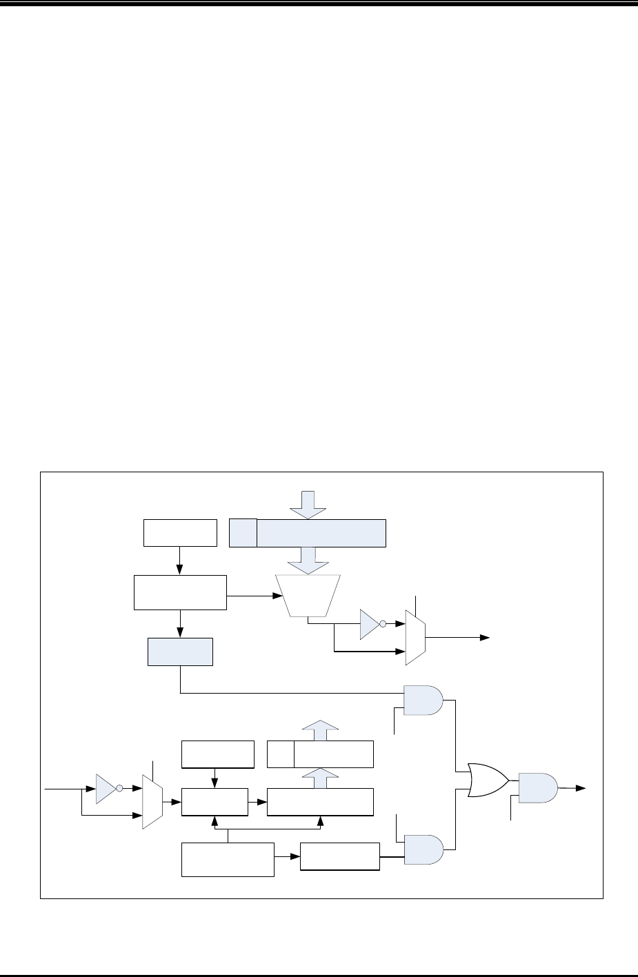
88 8.1 UART0
Version 1.0.0
Copyright ©2015, www.appotech.com. All Rights Reserved.
8 Universal Asynchronous
Receiver/Transmitter (UART)
8.1 UART0
8.1.1 Overview
UART0 is a serial port capable of asynchronous transmission. The UART0 can function in full duplex mode. Receive
data is buffered in a holding register. This allows the UART0 to start reception of a second incoming data byte before
software has finished reading the previous data byte. Figure 8-1 illustrates the UART0 Block Diagram.
When PSEL = 0
Receive pin (RX) – UART0RX0
Transmit pin (TX) – UART0TX0
When PSEL = 1
Receive pin (RX) – UART0RX1
Transmit pin (TX) – UART0TX1
TX Buffer
9 th
Bit
Data bus
MUX
UART TX
1
0UTTXDONE
UTTXINV
TXIE
UART RX 1
0
UTRXINV
Shift Register
RX Buffer
Data
Recovery
9 th
Bit
Data Bus
Baud Rate
Generator
Control Logic UTRXDONE
INT
RXIE
Baud Rate
Generator
Control Logic
U1IE
U1TXIF
U1RXIF
Figure 8-1 UART0 Block Diagram

8 Universal Asynchronous Receiver/Transmitter (UART) 89
Version 1.0.0
Copyright ©2015, www.appotech.com. All Rights Reserved.
8.1.2 UART0 Special Function Registers
Register 8-1 UARTCON – UART0 control
Position 7 6 5 4 3 2 1 0
Name UTSBS UTTXNB NBITEN UTEN UTTXINV UTRXINV TXIE RXIE
Default 0 1 0 0 0 0 0 0
Access R/W R/W R/W R/W R/W R/W R/W R/W
UTSBS: Stop Bit Select
0 = 1 bit as Stop Bit
1 = 2 bits as Stop Bit
UTTXNB: The ninth bit data of transmitter buffer. Write the ninth bit into this location that you want to transmit
NBITEN: Nine-BIT mode Enable Bit
0 = Eight-bit mode
1 = Nine-bit mode
UTEN: UART Enable Bit
0 = Disable UART module
1 = Enable UART module
UTTXINV: Transmit Invert Selection Bit
0 = Transmitter output without inverted
1 = Transmitter output inverted
UTRXINV: Receive Invert Selection Bit
0 = Receiver input without inverted
1 = Receiver input inverted
TXIE: Transmit Interrupt Enable
0 = Transmit interrupt disable
1 = Transmit interrupt enable
RXIE: Receive Interrupt Enable
0 = Receiver interrupt disable
1 = Receiver interrupt enable
Register 8-2 UARTSTA – UART0 status
Position 7 6 5 4 3 2 1 0
Name UTRXNB FEF RXIF TXIF - - - PSEL
Default x x 0 1 - - - 0
Access R/W R/W R/W RO - - - R/W
UTRXNB: The ninth bit data of receiver buffer
FEF: Frame Error Flag
0 = the stop bit is „1‟ in the last received frame
1 = the stop bit is „0‟ in the last received frame

90 8.1 UART0
Version 1.0.0
Copyright ©2015, www.appotech.com. All Rights Reserved.
RXIF: RX Interrupt Flag
0 = RX not done
1 = RX done
TXIF: TX Interrupt Flag
0 = TX not done
1 = TX done
Writing data to UTBUF will clear this flag.
PSEL: UART0 Port Select
0 = Select UART0RX0 and UART0TX0
UART0RX0: P34
UART0TX0: P16
1 = Select UART0RX1 and UART0TX1
UART0RX1: P00
UART0TX1: P01
Register 8-3 UARTBAUDL – UART0 Baud Rate Low Byte
Position 7 6 5 4 3 2 1 0
Name UARTBAUDL
Default x x x x x x x x
Access WO WO WO WO WO WO WO WO
Register 8-4 UARTBAUDH – UART0 Baud Rate High Byte
Position 7 6 5 4 3 2 1 0
Name UARTBAUDH
Default 0 0 0 0 0 0 0 0
Access WO WO WO WO WO WO WO WO
UARTBAUD = {UARTBAUDH, UARTBAUDL}
Register 8-5 UARTDIV
Position 7 6 5 4 3 2 1 0
Name UARTDIV
Default 0 0 0 0 0 0 0 0
Access WO WO WO WO WO WO WO WO
Baud Rate =Fsys clock / [(UARTBAUD +1) x (UARTDIV + 1)]
Register 8-6 UARTDATA – UART0 Data
Position 7 6 5 4 3 2 1 0
Name UARTDATA
Default x x x x x x x x
Access R/W R/W R/W R/W R/W R/W R/W R/W
Write this location will load the data to transmitter buffer. And read this location will read the data from the receiver

8 Universal Asynchronous Receiver/Transmitter (UART) 91
Version 1.0.0
Copyright ©2015, www.appotech.com. All Rights Reserved.
buffer.
8.2 UART1
8.2.1 Overview
UART1 is a serial port capable of asynchronous transmission. The UART1 can function in normal and DMA full
duplex mode. Please sees PMUXCON0 bit 6 descriptions
when PMUXCON0[6] == 0
Receive pin (RX) – UART1RX0 (P17)
Transmit pin (TX) – UART1TX0 (P16)
Or PMUXCON0[6] == 1
Receive pin (RX) – UART1RX1 (BT_TX)
Transmit pin (TX) – UART1TX1 (BT_RX)
8.2.2 UART1 Special Function Registers
Register 8-7 UART1CON – UART1 control
Position 7 6 5 4 3 2 1 0
Name UTSBS UTTXNB NBITEN UTEN TXIE RXIE OVERFLOWIE DMASEL
Default 0 1 0 0 0 0 - 0
Access R/W R/W R/W R/W R/W R/W - R/W
UTSBS: Stop Bit Select
0 = 1 bit as Stop Bit
1 = 2 bits as Stop Bit
UTTXNB: The ninth bit data of transmitter buffer. Write the ninth bit into this location that you want to transmit
NBITEN: Nine-BIT mode Enable Bit
0 = Eight-bit mode
1 = Nine-bit mode
UTEN: UART Enable Bit
0 = Disable UART module
1 = Enable UART module
TXIE: Transmit Interrupt Enable
0 = Transmit interrupt disable
1 = Transmit interrupt enable
RXIE: Receive Interrupt Enable
0 = Normal Receive interrupt disable or AUTO DMA mode Receive one word Interrupt disable
1 = Normal Receive interrupt enable or AUTO DMA mode Receive one word Interrupt enable
OVERFLOWIE: Receive DMA overflow interrupt enable
0 = overflow Interrupt disable

92 8.2 UART1
Version 1.0.0
Copyright ©2015, www.appotech.com. All Rights Reserved.
1 = overflow Interrupt enable
DMASEL:AUTO DMA choose
0 = AUTO DMA mode off
1= AUTO DMA mode on
Register 8-8 UART1STA – UART1 status
Position 7 6 5 4 3 2 1 0
Name UART_GIIE - UTRXNB RX_BYTE_HIGH RXIF TXIF OVERFLOWIF RXKICK
Default 0 - x 0 0 1 0 0
Access R/W - R/W RO R/W R/W R/W WO
UART_GIE:UART Global Interrupt 15 Enable
0 = UART Global I Interrupt disable
1 = UART Global I Interrupt enable
UTRXNB: The ninth bit data of receiver buffer
RX_BYTE_HIGH : receive data high byte(only for DMA)
0 = waiting receive data low byte
1 = waiting receive data high byte
RXIF: UART RX Interrupt Flag
0 = Normal Receive or AUTO DMA mode Receive one word not done
1 = Normal Receive or AUTO DMA mode Receive one word done
In normal mode, it becomes “1” every byte, but in DMA mode, it becomes “1” every word.
TXIF: UART TX Interrupt Flag
0 = UART transmit not done
1 = UART transmit done
Writing data to UTBUF or Writing UARTDMATXCNT will clear this flag.
OVERFLOWIF: UART overflow Interrupt Flag
0 = UART overflow not done
1 = UART overflow done
RXKICK: UART DMA receive KICK start
0 = not KICK start
1 = KICK start
Register 8-9 UART1DIV – UART1 divide register
Position 7 6 5 4 3 2 1 0
Name UART1DIV
Default 0 0 0 0 0 0 0 0
Access R/W R/W R/W R/W R/W R/W R/W R/W

8 Universal Asynchronous Receiver/Transmitter (UART) 93
Version 1.0.0
Copyright ©2015, www.appotech.com. All Rights Reserved.
Register 8-10 UART1BAUD – UART1 Baud Rate register
Position 7 6 5 4 3 2 1 0
Name UART1BAUD
Default x x x x x x x x
Access WO WO WO WO WO WO WO WO
Baud Rate =Fsys clock / [(UARTDIV+1) (UART1BAUD + 1))
Register 8-11 UART1DATA – UART1 Data
Position 7 6 5 4 3 2 1 0
Name UART1DATA
Default x x x x x x x x
Access R/W R/W R/W R/W R/W R/W R/W R/W
Write this location will load the data to transmitter buffer. And read this location will read the data from the receiver
buffer.
Register 8-12 UARTDMATXCNT –UART1 DMA Transmit counter
Portion 7 6 5 4 3 2 1 0
Name UARTDMATXCNT
Default x x x x x x X x
Access WO WO WO WO WO WO WO WO
Nbyte = UARTDMATXCNT + 1
Register 8-13 UARTDMATXPTR–UART1 DMA Transmit Start Pointer byte
Portion 7 6 5 4 3 2 1 0
Name UARTDMATXPTR
Default x x x X x x X x
Access WO WO WO WO WO WO WO WO
In order to get the correct DMA Start Pointer, you should write this register twice. First write the higher byte, then the
low byte. DMA address only map to SRAM1.
Register 8-14 UARTDMARXPTR–UART1 DMA receive Start Pointer byte
Portion 7 6 5 4 3 2 1 0
Name UARTDMARXPTR
Default x x x X x x X x
Access WO WO WO WO WO WO WO WO
In order to get the correct DMA Start Pointer , you should write this register twice. First write the higher byte, then the
low byte. DMA address only map to SRAM1.
Register 8-15 UART1MINUS–UART1 DMA receive data minus byte count by CPU
Portion 7 6 5 4 3 2 1 0
Name UART1MINUS
Default x x x X x x X x

94 8.2 UART1
Version 1.0.0
Copyright ©2015, www.appotech.com. All Rights Reserved.
Access WO WO WO WO WO WO WO WO
Nbyte = UART1MINUS+ 1'b1
Register 8-16 UART1POINTL–UAR1T DMA point by CPU read
Portion 7 6 5 4 3 2 1 0
Name UART1POINTL
Default x x x X x x X x
Access R/O R/O R/O R/O R/O R/O R/O R/O
Register 8-17 UART1POINTH–UART DMA point by CPU read high byte
Portion 7 6 5 4 3 2 1 0
Name UART1POINTH
Default x x x X x x X x
Access R/O R/O R/O R/O R/O R/O R/O R/O
Register 8-18 UART1LOOPCNT–UART1 DMA loop count
Position 7 6 5 4 3 2 1 0
Name overlowcnt dma_loop_cnt
Default 0 0 0 0 0
Access WO WO WO WO WO WO WO WO
overlowcnt: less than bytes UART receive data ram size
00 = 4 bytes
01 = 8 bytes
10 = 16 bytes
11 = 32 bytes
dma_loop_cnt::UART receive data ram size
000 = 16 bytes
001 = 32 bytes
010 = 64 bytes
011 = 128 bytes
100 = 256 bytes
101 = 512 bytes
110 = 1K bytes
111 = forbidden
Register 8-19 UART1CNTH–UART1 DMA receive count high byte
Portion 7 6 5 4 3 2 1 0
Name UART1CNTH
Defeault x x x X x x X x
Access R/O R/O R/O R/O R/O R/O R/O R/O

8 Universal Asynchronous Receiver/Transmitter (UART) 95
Version 1.0.0
Copyright ©2015, www.appotech.com. All Rights Reserved.
Register 8-20 UART1CNTL–UART1 DMA receive count low byte
Portion 7 6 5 4 3 2 1 0
Name UART1CNTL
Defeault x x x x x x x x
Access R/O R/O R/O R/O R/O R/O R/O R/O
8.3 Operation Guide
1)UART1 Normal mode Operation Flow:
1. Set IO in the correct direction.
2. Configure UARTDIV and UART1BAUD to choose sample rate and baud.
3. Enable UART1 module by setting UTEN to „1‟
4. Set TXIE or RXIE „to 1‟ if needed
5. Write data to UART1DATA
6. Wait for PND to change to „1‟, or wait for interrupt
7. Read received data from UART1DATA if needed
8. Go to Step 5 to start another process if needed or turn off UART1 by UTEN.
2)UART1 DMA Mode Operation Flow:
1. Set IO in the correct direction.
2. Configure UARTDIV and UART1BAUD to choose sample rate and baud.
3. Configure UART1CON Select DMA.
4. Write the start DMA address. for receive, Write data to UARTDMARXPTR
5. Enable UART module by setting UTEN to „1‟.
6. kick-start a DMA receive process
7. Wait overflow or delay some time ,read UART1CNTH and UART1CNTL,read data by write UART1MINUS
(UART1MINUS<{UART1CNTH,UART1CNTL}).
8. Write the start DMA address. for transmission, Write data to UARTDMATXPTR
9. Write data to UARTDMATXCNT to kick-start a DMA transmit process
10. Wait for PND to change to „1‟, or wait for interrupt

96 8.4 BT Control Register
Version 1.0.0
Copyright ©2015, www.appotech.com. All Rights Reserved.
8.4 BT Control Register
Register 8-21 BTCON1 – BT control register1
Position 7 6 5 4 3 2 1 0
Name BTC2RS BTCDCLKO BTCDCLKI BTRSTB Reserved XOSC26MEN
Default 0 0 0 0 0 0 0 0
Access R/W R/W R/W RO R/W R/W R/W R/W
BTC2RS: BTCON2 read select
0 = read BTCONT register
1 = read BT output state
BTCDCLKO: BT CDCLK output state
BTCDCLKI: BT CDCLK input state
XOSC26MEN: BT xosc26M enable
0 = disable
1 = enable
Register 8-22 BTCON2 – BT control register2
Position 7 6 5 4 3 2 1 0
Name BTTX BTRX BTCTS BTTESTEN BTGPIO10 BTGPIO9 BTGPIO5 BTGPIO4
Default 0 0 0 0 0 0 0 0
Access R/W R/W R/W R/W R/W R/W R/W R/W
write: write date to BT
read: depend on BTCON1[5]

9 Direct Memory Access (DMA) 97
Version 1.0.0
Copyright ©2015, www.appotech.com. All Rights Reserved.
9 Direct Memory Access (DMA)
9.1 DMA for IRAM
There is a DMA Arbiter to schedule all the DMA access to IRAM, it provide 12 DMA channels for IRAM DMA.
The following peripherals support IRAM DMA (Priority from high to low).
1. USB
2. SDC
3. UART1
4. Bit fetcher
5. SPI1
6. AGC
7. IIS
8. SPI0
9. FFT
10. Key Tone
For IRAM access, the DMA Arbiter has higher priority than CPU MOVX, MOVC and instruction code fetching. So
DMA will not be interrupted by CPU read or write on-chip SRAM. When DMA is transferring and a CPU access
occurs, the CPU will hold on the current accessing and try again next clock cycle.
9.2 DMA for RAM2
There is a DMA Arbiter to schedule all the DMA access to RAM2, it provide 7 DMA channels for RAM2 DMA.
The following peripherals support RAM2 DMA (Priority from high to low).
1. USB
2. Output Buffer
3. SDC
4. SPI0
5. SPI1
6. Uart1
7. IIS
For RAM2 access, the DMA Arbiter has higher priority than CPU MOVX, MOVC and instruction code fetching. So
DMA will not be interrupted by CPU read or write on-chip SRAM. When DMA is transferring and a CPU access occur,
the CPU will hold on the current accessing and try again next clock cycle.
9.3 DMA for DECRAM
There is a DMA Arbiter to schedule all the DMA access to DECRAM, it provide 5 DMA channels for DECRAM DMA.

98 9.4 DMA for IROM
Version 1.0.0
Copyright ©2015, www.appotech.com. All Rights Reserved.
The following peripherals support DECRAM DMA (Priority from high to low).
1. Huffman
2. Audio decode buffer
3. SDC
4. SPI0
5. IIS
For DECRAM access, the DMA Arbiter has higher priority than CPU MOVX, MOVC and instruction code fetching. So
DMA will not be interrupted by CPU read or write on-chip SRAM. When DMA is transferring and a CPU access occur,
the CPU will hold on the current accessing and try again next clock cycle.
9.4 DMA for IROM
There is a DMA Arbiter to schedule all the DMA access to IROM, it provide 1 DMA channel for IROM DMA.
The following peripherals support IROM DMA (Priority from high to low).
1. Huffman decoder
For IROM access, the DMA Arbiter has higher priority than CPU MOVC and instruction code fetching. So DMA will
not be interrupted by CPU read IROM. When DMA is transferring and a CPU access occur, the CPU will hold on the
current accessing and try again next clock cycle.
10 IR receiver 99
Version 1.0.0
Copyright ©2015, www.appotech.com. All Rights Reserved.
10 IR receiver
CW6687B provides a digital IR receiver, it can receive IR data followed by CPU, it also can read IR data from the IR
data buffer.
10.1 IR frame format
Figure 10-1 shows the IR data frame format
9ms 45ms 32 bits data
Figure 10-1 IR data frame format
Figure 10-2 shows the IR repeat frame format
9ms 2.25 0.56
Figure 10-2 IR repeat frame format
Figure 10-3 shows the IR bit 0 and bit 1 format
0.56ms
1.125ms
0.56ms
2.25ms
BIT 0 BIT 1
Figure 10-3 IR bit frame format

100 10.2 IR Receiver Control Registers
Version 1.0.0
Copyright ©2015, www.appotech.com. All Rights Reserved.
10.2 IR Receiver Control Registers
Register 10-1 IRCON0 - IR receiver control 0 register
Position 7 6 5 4 3 2 1 0
Name - - - IRPINSEL IRREPEAT IRPND IRIE IREN
Default 0 0 0 0 0 0 0 0
Access RO RO RO R/W RO R/W R/W R/W
IRPINSEL: IR input pin select
0 = P07 as IR receiver input
1 = P33 as IR receiver input
IRREPEAT: IR receiver repeating data
0 = Not repeat
1 = Repeat
IRPND: IR receiver done
0 = Undone
1 = Done
IRIE: IR interrupt enable
0 = Disabled
1 = Enabled
IREN: IR enable
0 = Disabled
1 = Enabled
Register 10-2 IRCON1 - IR receiver control 1 register
Position 7 6 5 4 3 2 1 0
Name IRCON1
Default 0 0 0 0 0 0 0 0
Access WO WO WO WO WO WO WO WO
The IRCON1 is the entrance for five 8-bit control registers: ONEFULL, ZEROCYC, REPEATCNT, ENDCONT and
BEGINCNT. And IRCON1 must be written five times to update all the five control registers.
First time for the ONEFULL.
Position 7 6 5 4 3 2 1 0
Name ONEFULL
Default 1 0 0 1 1 1 0 0
When IR clock is 1 MHz, ONEFULL*16*CLKCYC us is the time of IRDATA error. It is recommended to set ONEFULL
to 0x9C. (NOTE: ONEFULL*16 > BIT 1 cycle),
When IR clock is 32 KHz, ONEFULL*CLKCYC us is the time of IRDATA error. It is recommended to set ONEFULL to
0x5E(NOTE: ONEFULL*8 > BIT 1 cycle)
Second time for the ZEROCYC.
Position 7 6 5 4 3 2 1 0
Name ZEROCYC

10 IR receiver 101
Version 1.0.0
Copyright ©2015, www.appotech.com. All Rights Reserved.
Default 0 1 0 1 0 0 0 0
When IR clock is 1 MHz, ZEROCYC*16*CLKCYC us is the cycle of IR BIT 0 and BIT 1 division. It is recommended
to set ZEROCYC to 0x50. (NOTE: BIT 0 cycle < ZEROCYC*8 < BIT 1 cycle )
When IR clock is 32 KHz, ZEROCYC*CLKCYC us is the cycle of IR BIT 0 and BIT 1 division. It is recommended to
set ZEROCYC to 0x28 (NOTE: BIT 0 cycle < ZEROCYC < BIT 1 cycle)
Third time for the REPEATCNT.
Position 7 6 5 4 3 2 1 0
Name REPEATCNT
Default 0 0 0 0 0 1 0 0
When IR clock is 1 MHz, REPEATCNT*512*CLKCYC us is the IR repeat pulse (2.3ms). It is recommended to set
REPEATCNT to 0x04.
When IR clock is 32 KHz, REPEATCNT*32*CLKCYC us is the IR repeat pulse (2.3ms). It is recommended to set
REPEATCNT to 0x02.
Fourth time for the ENDCONT.
Position 7 6 5 4 3 2 1 0
Name ENDCONT
Default 1 0 0 0 0 0 0 0
When IR clock is 1 MHz, ENDCONT *512*CLKCYC us is the IR incept high (4ms). It is recommended to set
ENDCONT to 0x08.
When IR clock is 32 KHz, ENDCONT *32*CLKCYC us is the IR incept high (4ms). It is recommended to set
ENDCONT to 0x09.
Fifth time for the BEGINCNT.
Position 7 6 5 4 3 2 1 0
Name BEGINCNT
Default 0 0 0 1 0 0 0 1
When IR clock is 1 MHz, BEGINCNT * 512*CLKCYC us is the IR incept low (9ms). It is recommended to set
BEGINCNT to 0x11.
When IR clock is 32 KHz, BEGINCNT *32*CLKCYC us is the IR incept low (9ms). It is recommended to set
BEGINCNT to 0x08.
NOTE: When IR clock is 1 MHz and BEGINCNT or ENDCNT or REPEATCNT is configured to N,the detect range is
N*512*cycle ~ (N*512+511)*cycle.
NOTE: when IR clock is 32 KHz and BEGINCNT or ENDCNT or REPEATCNT is configured to N,the detect range is
N*32*cycle ~ (N*32+31)*cycle
Register 10-3 IRDAT0 - IR receiver data buffer0 register
Position 7 6 5 4 3 2 1 0
Name IRDAT0
Default 0 0 0 0 0 0 0 0
Access RO RO RO RO RO RO RO RO
Register 10-4 IRDAT1 - IR receiver data buffer1 register

102 10.3 IR Receiver Operation Guide
Version 1.0.0
Copyright ©2015, www.appotech.com. All Rights Reserved.
Position 7 6 5 4 3 2 1 0
Name IRDAT1
Default 0 0 0 0 0 0 0 0
Access RO RO RO RO RO RO RO RO
Register 10-5 IRDAT2 - IR receiver data buffer2 register
Position 7 6 5 4 3 2 1 0
Name IRDAT2
Default 0 0 0 0 0 0 0 0
Access RO RO RO RO RO RO RO RO
Register 10-6 IRDAT3 - IR receiver data buffer3 register
Position 7 6 5 4 3 2 1 0
Name IRDAT3
Default 0 0 0 0 0 0 0 0
Access RO RO RO RO RO RO RO RO
10.3 IR Receiver Operation Guide
1. Configure IR clock (CLKCON2);
2. Configure IRCON1 if needed;
3. Configure IRCON0;
4. Wait IRPND or IR interrupt;
5. Read IRDAT0/1/2/3.

11 SPI 103
Version 1.0.0
Copyright ©2015, www.appotech.com. All Rights Reserved.
11 SPI
11.1 SPI0
SPI0 can serve as master or slave. It can operate in normal or DMA mode.
SPI0 map to three group ports configured by PWKEDGE[6] and SPICON[3]:
Group0 - P27, P25, P26;
Group1 - P04, P06, P05;
Group2 - P14, P00, P34.
Group3 - P30(P40), P31, P32
When PWKEDGE[6]=0 and SPI0CON.3 = 0, Group0 activated
2wire mode: P2.6 as SPI0CLK0, P2.7 as SPI0DIDO0;
3wire mode: P2.6 as SPI0CLK0, P2.7 as SPI0DO2, P2.5 as SPI0DI0.
When PWKEDGE[6]=0 and SPI0CON.3 = 1, Group1 activated
2wire mode: P0.5 as SPI0CLK1, P0.4 as SPI0DIDO1;
3wire mode: P0.5 as SPI0CLK1, P0.4 as SPI0DO1, P0.6 as SPI0DI1.
When PWKEDGE[6]=1 and SPI0CON.3 = 0 Group2 activated
2wire mode: P3.4 as SPI0CLK2, P1.4 as SPI0DIDO2;
3wire mode: P3.4 as SPI0CLK2, P1.4 as SPI0DO2, P0.0 as SPI0DI2.
When PWKEDGE[6]=1 and SPI0CON.3 = 1, Grop3 activated
2wire mode: P3.0 as SPI0CLK3, P3.2 as SPI0DIDO3;
3wire mode: P3.0 as SPI0CLK3, P3.2 as SPI0DO3, P3.1 as SPI0DI3.
when PMUXCON0[5] = 1 P4.0 as SPI0CLK3
11.1.1 SPI0 Special Function Registers
Register 11-1 SPI0CON – SPI0 control
Position 7 6 5 4 3 2 1 0
Name SPI0PND SPI0SM SPI0RT SPI0WS SPI0PS0 SPI0EDGE SPI0IDST SPI0EN
Default 1 0 0 0 0 0 0 0
Access RO R/W R/W R/W R/W R/W R/W R/W
SPI0PND: SPI0 Pending bit (read only, writing SPI0BUF will clear this bit)
0 = Transmission is not finish
1 = Transmission finish

104 11.1 SPI0
Version 1.0.0
Copyright ©2015, www.appotech.com. All Rights Reserved.
SPI0SM: SPI0 mode selection
0 = Master mode
1 = Slave mode
SPI0RT: SPI0 RX/TX select bit in 2-wire mode or DMA mode
0 = TX
1 = RX
In 3-wire mode, SPI0 can both Transmit and receive at the same time. But when using DMA mode or 2-wire mode,
just one direction (TX or RX) is allowed. Use this bit to select TX or RX.
SPI0WS: SPI0 2-wire mode/3-wire mode select bit
0 = 3-wire mode
1 = 2-wire mode
SPI0PS0: SPI0 Port select 0
0 = Select P27, P25, P26 when SPI0PS1 = 0; Select P14, P00, P34 when SPI0PS1 = 1
1 = Select P04, P06, P05 when SPI0PS1 = 0
SPI0EDGE: SPI0 sampling edge select bit
When SPI0IDST = 0:
0 = Sample at falling edge
1 = Sample at rising edge
When SPI0IDST = 1:
0 = Sample at rising edge
1 = Sample at falling edge
SPI0IDST: SPI0 clock signal idle state
0 = Clock signal stays at 0 when idle
1 = Clock signal stays at 1 when idle
SPI0EN: SPI0 enable bit
0 = SPI0 disable
1 = SPI0 enable
Register 11-2 SPIBAUD – SPI0 Baud Rate
Position 7 6 5 4 3 2 1 0
Name SPIBAUD
Default x x x x x x x x
Access WO WO WO WO WO WO WO WO
Baud rate = Fsystem_clock / [2(SPIBAUD+1)]
Register 11-3 SPI0BUF – SPI0 Data Buffer
Position 7 6 5 4 3 2 1 0
Name SPI0BUF
Default x x x x x x x X
Access R/W R/W R/W R/W R/W R/W R/W R/W

11 SPI 105
Version 1.0.0
Copyright ©2015, www.appotech.com. All Rights Reserved.
Register 11-4 SPIDMACNT – SPI0 DMA counter
Position 7 6 5 4 3 2 1 0
Name SPIDMACNT
Default x x x x x x x x
Access WO WO WO WO WO WO WO WO
Nunit = SPIDMACNT + 1
Nbyte = Nunit * 2 = (SPIDMACNT + 1) * 2
Register 11-5 SPIDMAPTRH– SPI0 DMA Start Pointer high byte
Position 7 6 5 4 3 2 1 0
Name SPIDMAPTRH
Default x x x x x x x x
Access WO WO WO WO WO WO WO WO
Register 11-6 SPIDMAPTRL– SPI0 DMA Start Pointer low byte
Position 7 6 5 4 3 2 1 0
Name SPIDMAPTRL
Default x x x x x x x x
Access WO WO WO WO WO WO WO WO
11.1.2 SPI0 Operation Guide
When SPI0CON1.1=0,
SPI0 Normal Mode Operation Flow:
1. Set IO in the correct direction.
2. Select SPI0RT in 2-wire mode if 2-wire mode is selected
3. Select master mode or slave mode
4. Configure clock frequency when master mode is selected in step 3
5. Select one of the four timing modes
6. Enable SPI0 module by setting SPI0EN to „1‟
7. Set SPI0IE to „1‟ if needed
8. Write data to SPI0BUF to kick-start the process
9. Wait for SPI0PND to change to „1‟, or wait for interrupt
10. Read received data from SPI0BUF if needed
11. Go to Step 8 to start another process if needed or turn off SPI0 by clearing SPI0IE and SPI0EN
SPI0 DMA Mode Operation Flow:
1. Set IO in the correct direction.
2. Select SPI0RT for DMA direction
3. Select master mode or slave mode
4. Configure clock frequency when master mode is selected in step 3

106 11.2 SPI1
Version 1.0.0
Copyright ©2015, www.appotech.com. All Rights Reserved.
5. Select one of the four timing modes
6. Enable SPI0 module by setting SPI0EN to „1‟
7. Set SPI0IE „1‟ if needed
8. Write the start address to SPI0DMASP
9. Write data to SPI0DMACNT to kick-start a DMA process
10. Wait for SPI0PND to change to „1‟, or wait for interrupt
11. Go to Step 8 to start another DMA process if needed or turn off SPI0 by clearing SPI0IE and SPI0EN
11.2 SPI1
CW6687B SPI1 is an accelerated SPI. It can serve as master only. It can operate in normal or DMA mode. Please
see PMUXCON0 bit 5 descriptions
SPI1 uses 2 pins for 2 wire mode:
Serial Data (SPIDIDO1) – P04
Serial Clock (SPICLK1) – P05
SPI1 uses 3 pins for 3 wire mode:
When SPI1_MAP = 0,
Serial Data Out (SPIDO1) – P04
Serial Data In (SPIDI1) – P06
Serial Clock (SPICLK1) – P05
When SPI1_MAP = 1,
Serial Data Out (SPIDO0) – P04
Serial Data In (SPIDI0) – P42
Serial Clock (SPICLK0) – 05
11.2.1 SPI1 Special Function Registers
Register 11–7 SPI1CON – SPI1 Configure Register
Position 7 6 5 4 3 2 1 0
Name SPI1PND DMAERR SPI1RT SPI1WS SPI1DEC SPI1EN
Default 1 0 0 0 0 0 0 0
Access R/W R/W R/W R/W R/W RO RO R/W
SPI1PND: SPI1 Pending bit (read only, writing SPI1BUF will clear this bit)
0 = Transmission has not finished
1 = Transmission finish
DMAERR: SPI1 DMA Error flag
0 = No DMA error
1 = DMA error happened.
SPI1RT: SPI1 RX/TX select bit in 2-wire or DMA mode

11 SPI 107
Version 1.0.0
Copyright ©2015, www.appotech.com. All Rights Reserved.
0 = TX
1 = RX
In 3-wire mode, SPI1 can both Transmit and receive at the same time. But if we use DMA mode or 2-wire mode, just
one direction (TX or RX) is allowed. Use this bit to select TX or RX.
SPI1WS: SPI1 2-wire mode/3-wire mode select bit
0 = 3-wire mode
1 = 2-wire mode
SPI1DEC:SPI1 decryption function enables
0 = Disabled
1 = Enabled
SPI1EN: SPI1 enable bit
0 = SPI1 disabled
1 = SPI1 enabled
Register 11–8 SPI1CON1 – SPI1 Configure Register1
Position 7 6 5 4 3 2 1 0
Name - - - - - - CRCEN ENCRYPT
Default - - - - - - 0 0
Access - - - - - - R/W R/W
CRCEN: SPI1 CRC enable when SPI1 receiving data
0 = Disabled
1 = Enabled
ENCRYPT: SPI1 output encryption function enable
0 = Disabled
1 = Enabled
NOTE: ENCRYPT and SPI1DEC cannot be 1 at the same time.
Register 11–9 SPI1BUF – SPI1 Data Buffer
Position 7 6 5 4 3 2 1 0
Name SPI1BUF
Default X x x x x x x X
Access R/W R/W R/W R/W R/W R/W R/W R/W
Write this location to load the data to transmitter buffer and kick start the SPI transmission, read this location to read
the data from the receiver buffer.
Register 11–10 SPI1DMASPH– SPI1 DMA Pointer
Position 7 6 5 4 3 2 1 0
Name - - SPI1DMASPH
Default 0 0 x x x x x x
Access - - WO WO WO WO WO WO
SPI DMA start address pointer, point to the start address in IRAM that the data to be transmitted or data to be stored.

108 11.2 SPI1
Version 1.0.0
Copyright ©2015, www.appotech.com. All Rights Reserved.
Register 11–11 SPI1DMASPL– SPI1 DMA Pointer
Position 7 6 5 4 3 2 1 0
Name SPI1DMASPL
Default x x x x x x x x
Access WO WO WO WO WO WO WO WO
Register 11–12 SPI1DMACNTH – SPI1 DMA Counter High byte
Position 7 6 5 4 3 2 1 0
Name SPI1DMACNTH
Default X X x X x x x x
Access WO WO WO WO WO WO WO WO
Register 11–13 SPI1DMACNTL – SPI1 DMA Counter Low Byte
Position 7 6 5 4 3 2 1 0
Name SPI1DMACNTL
Default X x x x x x x x
Access WO WO WO WO WO WO WO WO
SPI DMA counter, decide the amount of units to be transmitted or received. There are 2 bytes in a unit. DMA counter
ranges from 0 to 2047 words. Formula is as follows:
SPIDMACNT = {SPIDMACNTH, SPIDMACNTL}
Nunit = SPIDMACNT + 1
Nbyte = Nunit * 2 = (SPIDMACNT + 1) * 2
Write this location to enable DMA and kick start a DMA process .Caution: do not write 0 to this register.
Note: Must write SPIDMACNTH, then SPIDMACNTL, this order can't change !
Register 11–14 SPI1BAUD – SPI1 BAUD RATE
Position 7 6 5 4 3 2 1 0
Name SPI1BAUD
Default 0 0 0 0 0 0 0 0
Access R/W R/W R/W R/W R/W R/W R/W R/W
SPI Baud Rate, from 0 to 255
SPI Clock is System Clock /(SPI1BAUD + 1), If SPI1BAUD is 0, then SPI Clock is same as System Clock.
11.2.2 SPI1 Operation Guide
A. SPI Normal Mode Operation Flow:
1. Set IO in the correct direction.
2. Select SPI1WS in 2-wire mode or 3 wire mode.
3. Select SPI1RT for reception or transmission.
4. Configure clock frequency using bit SPI1SP.
5. Enable SPI module by setting SPI1EN „1‟
6. Set SPI1IE „1‟ if needed

11 SPI 109
Version 1.0.0
Copyright ©2015, www.appotech.com. All Rights Reserved.
7. Write data to SPI1BUF to kick-start the process
8. Wait for SPI1PND change to „1‟, or wait for interrupt
9. Read received data from SPI1BUF if needed
10. Go to Step 7 to start another process if needed or turn off SPI1 by clearing SPI1PND and SPI1EN
B. SPI DMA Mode Operation Flow:
1. Set IO in the correct direction.
2. Select SPI1RT for DMA direction
3. Select SPI1WS in 2-wire mode or 3 wire mode
4. Configure clock frequency using bit SPI1SP
5. Enable SPI module by setting SPI1EN „1‟
6. Set SPI1IE „1‟ if needed
7. Write the start address to SPI1DMASP
8. Write data to SPI1DMACNT to kick-start the DMA process.
9. Wait for bit SPI1PND to change to „1‟, or wait for interrupt
10. Go to Step 7 to start another DMA process if needed or turn off SPI by clearing SPI1PND and SPI1EN
110 12.1 EMI Control Registers
Version 1.0.0
Copyright ©2015, www.appotech.com. All Rights Reserved.
12 External Memory Interface (EMI)
CW6687B provides External Memory Interface (EMI) to accelerate data transfer. Figure 12-1 shows EMI timing.
EMIHTEMIST EMIPW
EMI_DATA(P2)
EMI_WEN(P3.3)
Figure 12-1 EMI timing
12.1 EMI Control Registers
Register 12-1 EMICON0 – EMI control0
Position 7 6 5 4 3 2 1 0
Name EMIEN EMIPW EMIHT EMIST
Default 1 0 0 0 0 0 0 0
Access R/W R/W R/W R/W R/W R/W R/W R/W
EMIEN:
When writing: EMI Enable
0 = Disable
1 = Enable
EMIPW: EMI pulse width
000 = 1 system clock cycle
001 = 2 system clock cycles
010 = 3 system clock cycles
011 = 4 system clock cycles
100 = 5 system clock cycles
101 = 6 system clock cycles
110 = 7 system clock cycles
111 = 8 system clock cycles
EMIHT: EMI hold time
00 = 1 system clock cycle

12 External Memory Interface (EMI) 111
Version 1.0.0
Copyright ©2015, www.appotech.com. All Rights Reserved.
01 = 2 system clock cycles
10 = 3 system clock cycles
11 = 4 system clock cycles
EMIST: EMI setup time
00 = 1 system clock cycle
01 = 2 system clock cycles
10 = 3 system clock cycles
11 = 4 system clock cycles
Register 12-2 EMICON1 – EMI control1
Position 7 6 5 4 3 2 1 0
Name EMIPND OUTSEL PWMEN EMIDMAB EMIDMAM EMIM
Default 1 0 0 0 0 0 0 0
Access RO R/W R/W R/W R/W R/W R/W R/W
EMIPND: When Read EMI done flag
0 = EMI is transmitting data
1 = EMI is IDLE
When writing “0”, clear write buffer counter; write to “1” affect another
OUTSEL: PWM output select
0 = LED anode display
1 = LED cathode display
PWMEN: PWM enable
0 = Disable
1 = Enable
EMIDMAB: EMI DMA converts byte select
00 = reserved
01 = 1 byte
10 = 2 byte
11 = 3 byte
EMIDMAM: EMI DMA mode
0 = no convert
1 = bit convert to byte
EMIM: EMI mode
0 = work when CPU kick start
1 = work with SPI1 DMA
Register 12-3 EMIBUF – EMI output buffer
Position 7 6 5 4 3 2 1 0
Name EMIBUF
Default x x x x x x x x
Access WO WO WO WO WO WO WO WO

112 12.1 EMI Control Registers
Version 1.0.0
Copyright ©2015, www.appotech.com. All Rights Reserved.
EMIBUF is the entrance of 6 bytes EMI output buffer. The 6 bytes EMI output buffer is emibuf0, emibuf1, emibuf2,
emibuf3, emibuf4 and emibuf5. When CPU writes to EMIBUF, internal counter will add “1”, CPU data is pushed to
corresponding buffer. You should clear internal counter by writing “0” to emicon1 bit 7;
PWM mode: should write eight times for eight channels PWM of P2
When EMIM = 0, emibuf0 will output to P2. Emibuf0 is updated with CPU write data.
When EMIM = 1 and in no convert mode, emibuf0 will output to P2. Emibuf0 is updated with SPI1 DMA data.
When SPI2EMI = 1 and in convert mode, there are 3 output modes:
Register 12-4 PMWBUF0/1/2/3/4/5/6/7 – PWM duty buffer0/1/2/3/4/5/6/7
Position 7 6 5 4 3 2 1 0
Name PWMBUF0/1/2/3/4/5/6/7
Default x x x x x x x x
Access WO WO WO WO WO WO WO WO
This register confige PWM duty.
PWM period is config by EMICON0[3:0] and EMICON0[6:4]. PWM period = pre counter * post counter * system
clock
EMICON0[6:4]: config pwm output period post counter
000 = 2
001 = 4
010 = 8
011 = 16
100 = 32
101 = 64
110 = 128
111 = 256
EMICON0[3:0]: config pwm output period pre counter
0xxx = 1
1000 = 2
1001 = 4
1010 = 8
1011 = 16
1100 = 32
1101 = 64
1110 = 128
1111 = 256
Corresponding bit 0 1
1 byte mode emibuf0 emibuf3

12 External Memory Interface (EMI) 113
Version 1.0.0
Copyright ©2015, www.appotech.com. All Rights Reserved.
Corresponding bit 0 1
2 byte mode emibuf0 emibuf1 emibuf3 emibuf4
3 byte mode emibuf0 emibuf1 emibuf2 emibuf3 emibuf4 emibuf5
When EMIM = 0 and EMIEN = 1, EMI transfer start by writing to EMIBUF.
When EMIM = 1 and EMIEN = 1, EMI transfer will be started by SPI DMA.
PWM Operation Guide
1. Configure EMICON1 register;
2. Read data from FFT output buffer;
3. Write data to PWMDAT register.

114 13.1 Features
Version 1.0.0
Copyright ©2015, www.appotech.com. All Rights Reserved.
13 Audio Terminal (DAC)
13.1 Features
CW6687B provides a high performance stereo 16-bit resolution audio DAC:
Sample Rate 8 / 11.025 / 12 / 16 / 22.05 / 24 / 32 / 44.1 / 48KHz
Low Clock Jitter Sensitivity
Soft Mute and -48Db Attenuator
Class AB headphone amplifier
32 Level analog Gain/attenuation from dB to dB
13.2 DAC Special Function Registers
There are 2 SFR to support DAC registers read/write function:
Register 13-1 ATADR - audio terminal address
Position 7 6 5 4 3 2 1 0
Name DONE DIR ATADR
Default x x x x x x x x
Access RW RW RW RW RW RW RW RW
DONE: read/write operation done flag
0 = read/write operation is done
1 =read/write operation is running
DIR: read/write direction select
0 =read register
1 = write register
ATADR: Address of DAC registers
Register 13-2 ATDAT - audio terminal data
Position 7 6 5 4 3 2 1 0
Name ATDAT
Default x x x x x x x x
Access RW RW RW RW RW RW RW RW
ATDAT:
After read operation, CPU reads this register to get the data.
Before write operation, CPU writes data to this register.
13.2.1 DAC Register Mapping
Table 13-1 DAC registers address mapping:

13 Audio Terminal (DAC) 115
Version 1.0.0
Copyright ©2015, www.appotech.com. All Rights Reserved.
Name Address Descriptions
DACCFG 0 DAC configuration register
DACSM 1 DAC soft mute configuration register
DACSPR 2 DAC sample rate register
DACVOLL 3 DAC volume setting low byte register
DACVOLH 4 DAC volume setting high byte register
DACVCON 5 DAC volume control register
TRIMCON1 6 DAC trim control register1
TRIMCON2 7 DAC trim control register2
TRREGLL 8 DAC left channel trim data register low byte
TRREGLH 9 DAC left channel trim data register high byte
TRREGRL 10 DAC right channel trim data register low byte
TRREGRH 11 DAC right channel trim data register high byte
EQCON1 12 EQ configuration register1
EQCOF 13 EQ coefficient FIFO
EQCON2 14 EQ configuration register2
EQVOLIN 15 EQ data input volume configuration register
DACLRMIX0 16 DAC L & R channel mixing coefficient 0
DACLRMIX1 17 DAC L & R channel mixing coefficient 1
DACLRMIX2 18 DAC L & R channel mixing coefficient 2
DACLRMIX3 19 DAC L & R channel mixing coefficient 3
13.2.2 Function of DAC Control Registers
Register 13-3 DACCFG - DAC configuration register
Position 7 6 5 4 3 2 1 0
Name - - - DIT_SEL MIX_EN OSSL DACEN
Default - - - 0 0 0
Access - - - RW RW RW
DIT_SEL: sdm dither signal select
0 = sine wave
1 = white noise
MIX_EN: DAC MIX enable
0 = Disabled
1 = Enabled
OSSL: DAC over sample mode select
0 = Normal speed mode
1 = Double speed mode
DACEN: DAC digital filter/delta-sigma modulator enable
0 = Disabled
1 = Enabled

116 13.2 DAC Special Function Registers
Version 1.0.0
Copyright ©2015, www.appotech.com. All Rights Reserved.
Register 13-4 DACSM - DAC soft mute configuration register
Position 7 6 5 4 3 2 1 0
Name DACSM
Default 0 1 1 1 1 1 1 0
Access RW RW RW RW RW RW RW RW
DAC soft mute configuration, the reset value of DACSM is 126, user should not change it.
Register 13-5 DACSPR - DAC sample rate register
Position 7 6 5 4 3 2 1 0
Name - - - - SRSEL
Default - - - - 0 0 0 1
Access - - - - RW RW RW RW
SRSEL: DAC/FM sample rate select
0000 = 48 KHz
0001 = 44.1 KHz
0010 = 32 KHz
0011 = Reserved
0100 = 24 KHz
0101 = 22.05 KHz
0110 = 16 KHz
0111 = Reserved
1000 = 12 KHz
1001 = 11.025 KHz
1010 = 8 KHz
1011 = Reserved
1100 = 48K synchronized with OBUF (+-0.8% max)
1101 = 44.1K synchronized with OBUF (+-0.8% max)
1110 = 32K synchronized with OBUF (+-0.8% max)
1111 = 16K synchronized with OBUF (+-0.8% max)
1011 = 8K synchronized with OBUF (+-0.8% max)
Register 13-6 DACVOLH - DAC volume setting high byte register
Position 7 6 5 4 3 2 1 0
Name DACVPND DACVOLH
Default 1 0 0 0 0 1 1 1
Access RW RW RW RW RW RW RW RW
DACVPND: DAC volume adjust done pending
Read “0”: not done
Read “1”: done
Write “0” clear pending
Write “1” affects nothing

13 Audio Terminal (DAC) 117
Version 1.0.0
Copyright ©2015, www.appotech.com. All Rights Reserved.
Register 13-7 DACVOLL– DAC volume setting low byte register
Position 7 6 5 4 3 2 1 0
Name DACVOLL
Default 1 1 1 1 1 1 1 1
Access R/W R/W R/W R/W R/W R/W R/W R/W
Note: When read DACVOLL and DACVOLH, the value isn‟t the setting value, but the actual DAC volume value
The DAC Volume multiple is : DACVOL/(2^11) where DACVOL is {DACVOLH,DACVOLL}
Example :
DACVOL = 0x07ff is 0x07ff/(2^11) = 1 = 0 DB
DACVOL = 0x7fff is 0x7fff/(2^11) = 16 ~= +24 DB
Register 13-8 DACVCON– DAC volume control register
Position 7 6 5 4 3 2 1 0
Name - - - DACVSET DACVSTEP DACVEN DACVSTEP
Default - - - 0 0 0 0 0
Access - - - WO R/W R/W R/W R/W
DACVSET: Direct set DAC volume value
Write “1” to direct set DAC volume value
Write “0” affects nothing
DACVEN: DAC volume adjust enable
0 = Disable DAC volume adjust, keep the current volume
1 = Enable DAC volume adjust
{ DACVSTEP2 , DACVSTEP}: DAC adjust volume steps
000 = Steps is “1”
001 = Steps is “2”
010 = Steps is “4”
011 = Steps is “8”
100 = Steps is “16”
101 = Steps is “32”
110 = Steps is “64”
111 = Steps is “128”
Register 13-9 TRIMCON1 - DAC trim control register1
Position 7 6 5 4 3 2 1 0
Name TRIMSPEED TRIMSTEP DITSEL TRIMSET DONESEL TRIMEN
Default 0 0 0 0 0 0 0 0
Access RW RW RW RW RW RW RW RW
TRIMSPEED: DAC trim speed control
00 = trim 1 step every 1 sample
01 = trim 1 step every 2 samples

118 13.2 DAC Special Function Registers
Version 1.0.0
Copyright ©2015, www.appotech.com. All Rights Reserved.
10 = trim 1 step every 3 samples
11 = trim 1 step every 4 samples
TRIMSTEP: DAC trim step control
00 = Trim Step is 1
01 = Trim Step is 2
10 = Trim Step is 4
11 = Trim Step is 8
DITSEL: DAC trim direction select
0 = Trim direction depend on DAC analog compare out
1 = Trim direction depend on software direction
TRIMSET: DAC trim vale set direct
0 = reserve
1 = set direct
DONESEL: trimming done condition select
0 = Depend on DAC analog compare edge
1 = Depend on match data
TRIMEN: DAC trimming enable
0 = Disabled
1 = Enabled
Register 13-10 TRIMCON2 - DAC trim control register2
Position 7 6 5 4 3 2 1 0
Name - - DIRETR DIRETL TRIMMTL TRIMMTR TMDONE TRIMKST
Default - - 0 0 0 0 0 0
Access - - RW RW RW RW RW RW
DIRETR: DAC right trim direction
0 = Trim data decrease one step one sample
1 = Trim data add one step one sample
DIRETL: DAC left trim direction
0 = Trim data decrease one step one sample
1 = Trim data add one step one sample
TRIMMTL: DAC left channel trimming data match
0 = Not match
1 = Match
TRIMMTR: DAC right channel trimming data match
0 = Not match
1 = Match
TMDONE: DAC trimming done
0 = Not done

13 Audio Terminal (DAC) 119
Version 1.0.0
Copyright ©2015, www.appotech.com. All Rights Reserved.
1 = Done
TRIMKST: DAC trimming kick start
Write 1 to kick start DAC trimming
Register 13-11 TRREGLL - DAC left channel trim data reg law byte
Position 7 6 5 4 3 2 1 0
Name TRIMREGLL
Default - - - - - - - -
Access RW RW RW RW RW RW RW RW
TRIMREGLL:
Write: DAC anticipant trimming data reg law byte
Read: DAC real trimming data law byte
Register 13-12 TRREGLH - DAC left channel trim data reg high byte
Position 7 6 5 4 3 2 1 0
Name TRIMREGLH
Default - - - - - - - -
Access RW RW RW RW RW RW RW RW
TRIMREGLL:
Write: DAC anticipant trimming data register high byte
Read: DAC real trimming data high byte
Register 13-13 TRREGRL- DAC right channel trim data reg law byte
Position 7 6 5 4 3 2 1 0
Name TRIMREGRL
Default - - - - - - - -
Access RW RW RW RW RW RW RW RW
TRIMREGRL:
Write: DAC anticipant trimming data register low byte
Read: DAC real trimming data low byte
Register 13-14 TRREGRH - DAC right channel trim data reg high byte
Position 7 6 5 4 3 2 1 0
Name TRIMREGRH
Default - - - - - - - -
Access RW RW RW RW RW RW RW RW
TRIMREGRH:
Write: DAC anticipant trimming data register high byte
Read: DAC real trimming data high byte

120 13.2 DAC Special Function Registers
Version 1.0.0
Copyright ©2015, www.appotech.com. All Rights Reserved.
13.2.3 EQ and DRC Control Register
Register 13-15 EQCON1 - EQ configuration register1
Position 7 6 5 4 3 2 1 0
Name DRCEN EQEN PEAKM COMPONLY STEREOSHARE EQBANDCNT
Default 0 0 0 0 0 0 0 0
Access R/W R/W R/W R/W R/W R/W R/W R/W
DRCEN: DRC enable bit
0 = disable
1 = enable
EQEN: EQ enable bit
0 = Disabled
1 = Enabled
PEAKM: DRC peak level detector mode select
0 = mode 0 (preferred)
1 = mode 1
COMPONLY : DRC Compressor
0 = DRC include Limiter, Compressor, Expander and Noise gate
1 =DRC just Limiter, Compressor only (preferred)
STEREOSHARE: stereo share one DRC select bits
0 = left right channel has respective DRC
1 =left right channel share joint DRC
EQBANDCNT: EQ BAND counters
Configuration the number of EQ BAND
Register 13-16 EQCON2 - EQ configuration register2
Position 7 6 5 4 3 2 1 0
Name DONE CFGADRCLR BUFINIT EQ_RST
Default 0 0 0 0
Access R/W WO WO WO
EQ_RST: EQ RST
0 = reset EQ
1 = release EQ rst
BUFINIT: EQ buffer clear
Write 1 kick start buffer initial
Write 0 is invalidation
CFGADRCLR: EQ cof address clear
Write 1 reset EQ cof address

13 Audio Terminal (DAC) 121
Version 1.0.0
Copyright ©2015, www.appotech.com. All Rights Reserved.
Write 0 is invalidation
DONE: EQ buffer initial done flag
1 = Done
0 = Not done
Register 13-17 EQCOF - EQ coefficient FIFO
Position 7 6 5 4 3 2 1 0
Name EQCOF
Default x x x x x x x x
Access WO WO WO WO WO WO WO WO
EQCOF:
As the coefficient is 24 bits, so write EQCOF three times low byte first ( = EQCOF*(2^22-1))
DRC coefficient is 24bits, write EQCOF three times low byte first(= DRCCOF*(2^18-1) reference DRC C model )
The order of coefficient as follow:
EQ coefficient:
EQ BAND0
Gain COF
24 bits
EQ BAND 0 COF0 or IIR BAND 0 COF0
EQ BAND 0 COF2 or IIR BAND 0 COF2
EQ BAND 0 COF1 or IIR BAND 0 COF1
EQ BAND 0 negative COF4 or IIR BAND 0 negative COF4
EQ BAND 0 negative COF5 or IIR BAND 0 negative COF5
EQ BAND1
EQ BAND 1 COF0 or IIR BAND 1 COF0
24 bits
EQ BAND 1 COF2 or IIR BAND 1 COF2
EQ BAND 1 COF1 or IIR BAND 1 COF1
EQ BAND 1 negative COF4 or IIR BAND 1 negative COF4
EQ BAND 1 negative COF5 or IIR BAND 1 negative COF5
EQ BANDn …… 24 bits
Reservation 0x000000 24 bits
DRC at_comexp DRC attack time coefficient for compressor 24 bits
DRC rt_comexp DRC release time coefficient for compressor 24 bits
DRC at_lim DRC attack time coefficient for limiter 24 bits
DRC rt_lim DRC release time coefficient for limiter 24 bits
DRC LT DRC Limiter Thresholds DB (Limiter exceed LT) 24 bits
DRC LS DRC Limiter slope 24 bits
DRC CT DRC Compressor Thresholds DB (Compressor rang LT to CT) 24 bits
DRC CS DRC Compressor slope 24 bits
DRC ET DRC Expander Thresholds DB (Expander range ET to NT) 24 bits
DRC ES DRC Expander slope 24 bits
DRC NT DRC Noise Gate Thresholds DB (Attenuate below NT) 24 bits
DRC NS DRC Noise Gate slope 24 bits
DRC GAIN DRC gain offset 24 bits

122 13.2 DAC Special Function Registers
Version 1.0.0
Copyright ©2015, www.appotech.com. All Rights Reserved.
DRC TAV The averaging coefficient 24 bits
Register 13-18 EQVOLIN - EQ data input volume configuration register
Position 7 6 5 4 3 2 1 0
Name EQVOLIN
Default x x x x x x x x
Access W/R W/R W/R W/R W/R W/R W/R W/R
The input volume of EQ data rang from 0x0000 to 0x7fff, write twice high byte first.
0x7fff represent 0 db
0x000 represent silence
Register 13-19 DACLRMIX0: DAC L & R channel mixing coefficient register0
Position 7 6 5 4 3 2 1 0
Name DACLRMIX0
Default 0 1 1 1 1 1 1 1
Access RW RW RW RW RW RW RW RW
DAC L & R channel mixing coefficient 0
NOTE: DACLRMIX0 and DACLRMIX1 are used to control how L channel is combined with R channel to generate
the final L channel output. The content of DACLRMIX0 and DACLRMIX1 each represents a 8 bit signed number
which ranges from -128 ~ 127. the L channel output is calculated from the following equation:
Lout = Lin* DACLRMIX0/128 + Rin* DACLRMIX1/128
Register 13-20 DACLRMIX1 DAC L & R channel mixing coefficient register1
Position 7 6 5 4 3 2 1 0
Name DACLRMIX1
Default
Access RW RW RW RW RW RW RW RW
DAC L & R channel mixing coefficient 1 register
NOTE: DACLRMIX0 and DACLRMIX1 are used to control how L channel is combined with R channel to generate
the final L channel output. The content of DACLRMIX0 and DACLRMIX1 each represents a 8 bit signed number
which ranges from -128 ~ 127. the L channel output is calculated from the following equation:
Lout = Lin* DACLRMIX0/128 + Rin* DACLRMIX1/128
Register 13-21 DACLRMIX2 DAC L & R channel mixing coefficient register2
Position 7 6 5 4 3 2 1 0
Name DACLRMIX2
Default 0 0 0 0 0 0 0 0
Access RW RW RW RW RW RW RW RW
DAC L & R channel mixing coefficient register 2
NOTE: DACLRMIX2 and DACLRMIX3 are used to control how R channel is combined with L channel to generate
the final R channel output. The content of DACLRMIX2 and DACLRMIX3 each represents a 8 bit signed number
which ranges from -128 ~ 127. the R channel output is calculated from the following equation:

13 Audio Terminal (DAC) 123
Version 1.0.0
Copyright ©2015, www.appotech.com. All Rights Reserved.
Rout = Lin* DACLRMIX2/128 + Rin* DACLRMIX3/128
Register 13-22 DACLRMIX3 DAC L & R channel mixing coefficient 3
Position 7 6 5 4 3 2 1 0
Name DACLRMIX3
Default 0 1 1 1 1 1 1 1
Access RW RW RW RW RW RW RW RW
DAC L & R channel mixing coefficient register 3
NOTE: DACLRMIX2 and DACLRMIX3 are used to control how R channel is combined with L channel to generate
the final R channel output. The content of DACLRMIX2 and DACLRMIX3 each represents a 8 bit signed number
which ranges from -128 ~ 127. the R channel output is calculated from the following equation:
Rout = Lin* DACLRMIX2/128 + Rin* DACLRMIX3/128
Register 17-28 KVCCON– Key Voice control
Position 7 6 5 4 3 2 1 0
Name - - - - - - MPEN KEYEN
Default x x x x x x 1 0
Access x x x x x x R/W R/W
KEY_DMA_ADRH: Key voice DMA high address
MPEN: MP3 is playing enable
0 = Disable MP3 play when plays key voice
1 = Enable MP3 play when plays key voice
KEYEN: Key Voice enable
0 = Disabled
1 = Enabled
Register 17-29 KVCCON2– Key Voice control
Position 7 6 5 4 3 2 1 0
Name KVCCYC[4:0] KVV[2:0]
Default 0 0 0 0 1 1 1 1
Access R/W R/W R/W R/W R/W R/W R/W R/W
KVCCON2: key voice control
KVV [2:0]: key voice volume control
000 = volume div 128
001 = volume div 64
010 = volume div 32
011 = volume div 16
100 = volume div 8
101 = volume div 4
110 = volume div 2
111 = 0db

124 13.3 Operation Guide
Version 1.0.0
Copyright ©2015, www.appotech.com. All Rights Reserved.
KVCCYC [4:0]: key voice plays cycle control
The real cycle of key voice play is KVCCYC [4:0] * 8.
Register 17-30 KVCADR– Key Voice DMA address
Position 7 6 5 4 3 2 1 0
Name KEY_DMA_ADR
Default x x x x x x x x
Access WO WO WO WO WO WO WO WO
When configure key voice DMA address, should write this register three times. First configure the DMA start high
address, second configure the DMA start low address, and third configure the DMA end low address. It can only
change between 0 to 0xff
13.3 Operation Guide
13.3.1 DAC Operation Guide
1. Configure DACVOLL & DACVOLH
2. Configure DACVCON
3. Clear DACVPND to kick start adjust volume
13.3.2 EQ Operation Guide
1. Configure EQCON2 to release The rest of EQ
2. Configure EQCON1 BIT 6 to kick initiate the buffer ram and wait done
3. Configure EQVOLIN
4. Configure EQCOF to initiate coefficient
5. Configure EQCON1 to enable EQ
Notice:
1) If user wants to change the coefficient of EQ he/she must configure EQCON1 disable EQ, then repeat upwards
operation guide flow.

14 SARADC 125
Version 1.0.0
Copyright ©2015, www.appotech.com. All Rights Reserved.
14 SARADC
14.1 Features
CW6687B provides an 11-channel moderate conversion speed and a moderate resolution 10-bit successive
approximated register Analog to Digital Converter (SARADC) for users to develop applications in the following
areas:
Voice grade applications
Audio applications requiring moderate performance
Measurement requiring moderate performance and speed
SARADC conversion clock must be slower than 1 MHz
14.2 ADC Pin Mapping
Table 14-1 pin used
ADC Channel Function Description
ADC10 TP3
ADC9 TP2
ADC8 P26 Only for PIN detected, Not for ADKEY
ADC7 LDO Band GAP Reference voltage 0.864V
ADC6 LDO in 1/2 Battery voltage
ADC5 P13 Normal ADC channel
ADC4 P30 Normal ADC channel
ADC3 P22 Normal ADC channel
ADC2 P14 Normal ADC channel
ADC1 P21 Normal ADC channel
ADC0 P33 Normal ADC channel
14.3 SARADC Special Function Registers
Register 14-1 ADCCON– SARADC control
Position 7 6 5 4 3 2 1 0
Name ADCGO EOC TMREN ADCTL ADCEN ADCSEL
Default 0 0 x x 0 0 0 0
Access R/W RO R/W R/W R/W R/W R/W R/W
ADCGO: ADC Conversion Start
When read:
0 = Conversion finished
1 = Conversion not finished

126 14.3 SARADC Special Function Registers
Version 1.0.0
Copyright ©2015, www.appotech.com. All Rights Reserved.
When write:
0 = N/A
1 = Start conversion
EOC: Check if end of conversion
0 = Finished
1 = Not finished
TMREN: Timer Input Enable
0 = Disabled
1 = Enabled
ADCTL: Timer Source Select
0 = Timer0
1 = Timer1
ADCEN: ADC Module Enable
0 = Disabled
1 = Enabled
ADCS3, ADCSEL: ADC Channel Select
0000 = P3.3 (ADC0)
0001 = P2.1 (ADC1)
0010 = P1.4 (ADC2)
0011 = P2.2 (ADC3)
0100 = P3.0 (ADC4)
0101 = P1.3 (ADC5)
0110 = 1/2 Battery voltage
0111 = LDO_BG. 0.864V
1000 = P26 (ADC8,Only for PIN detected, Not for ADKEY)
1001 = TP2
1010 = TP3
Register 14-2 ADCMODE– SARADC mode control
Position 7 6 5 4 3 2 1 0
Name - - - ADCS3 AUTOS ADCSEL_SH
Default 0 0 0 0 0 0 0 0
Access RO RO RO R/W R/W R/W R/W R/W
ADCS3: ADC Channel Select 3
ADCSEL_SH: ADCSEL shadow
AUTOS: Auto channel switching mode
0 = Not switch
1 = Auto load ADCSEL_SH into ADCSEL after conversion finished
Register 14-3 ADCBAUD– SARADC baud rate control

14 SARADC 127
Version 1.0.0
Copyright ©2015, www.appotech.com. All Rights Reserved.
Position 7 6 5 4 3 2 1 0
Name - - ADCBAUD
Default - - x x x x x x
Access - - WO WO WO WO WO WO
ADC conversion clock = system clock / (2 x (ADCBAUD + 1))
Register 14-4 ADCDATAL– SARADC Buffer low byte control
Position 7 6 5 4 3 2 1 0
Name ADCDATAL - - - - - -
Default x x - - - - - -
Access RO RO - - - - - -
Register 14-5 ADCDATAH– SARADC Buffer high byte control
Position 7 6 5 4 3 2 1 0
Name ADCDATAH
Default x x x x x x x x
Access RO RO RO RO RO RO RO RO
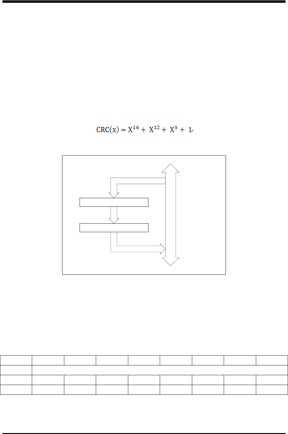
128 15.1 CRC16
Version 1.0.0
Copyright ©2015, www.appotech.com. All Rights Reserved.
15 CRC16 /LFSR16/LFSR32
15.1 CRC16
15.1.1 Features
Cyclic Redundancy Check (CRC) is an error-checking code that is widely used in data communication systems and
other serial data transmission system. CRC is based on polynomial manipulation using modular arithmetic. The
device supports CRC by a CRC circuit module. The CRC FIFO supports CRC-CCITT.
The CRC-CCITT polynomial is defined as:
Figure 15-1 shows CRC FIFO block diagram.
CRC FIFO High Byte
CRC FIFO Low Byte
CPU Read CRC FIFO
CPU Write CRC FIFO
CPU data BUS
Figure 15-1 CRC FIFO block diagram
Write CRCREG to initial CRC register. Write data into CRCFIFO after initialization, and data will be shifted into
module from low bit to high bit. Get the results by reading CRCRES0 and CRCRES1.
15.1.2 CRC16 Special Function Registers
Register 15-1 CRCREG– CRC initial register
Position 7 6 5 4 3 2 1 0
Name CRCREG
Default 1 1 1 1 1 1 1 1
Access WO WO WO WO WO WO WO WO
Write this location will initial CRC register.
Note: To initialize the CRC register, user needs to write 2 bytes to CRCREG for CRC16 (High byte first).
15 CRC16 /LFSR16/LFSR32 129
Version 1.0.0
Copyright ©2015, www.appotech.com. All Rights Reserved.
Register 15-2 CRCFIFO– CRC FIFO control
Position 7 6 5 4 3 2 1 0
Name CRCFIFO
Default x x x x x x x x
Access WO WO WO WO WO WO WO WO
Write this location will load the data to CRC module;
Register 15-3 CRCRES0– CRC result 0 control
Position 7 6 5 4 3 2 1 0
Name CRCRES0
Default x x x x x x x x
Access RO RO RO RO RO RO RO RO
Register 15-4CRCRES1– CRC result 1 control
Position 7 6 5 4 3 2 1 0
Name CRCRES1
Default x x x x x x x x
Access RO RO RO RO RO RO RO RO
15.2 LFSR16
15.2.1 Features
Software can control lfsr16, or enable CRCEN of SPI1CON1 [1], hardware can auto trigger lfsr16 when spi1 receive
data.
The LFSR16 polynomial is defined as:
15.2.2 LFSR16 Special Function Register
Register 15-5 LFSR16_DAT0– LFSR16 data 0
Position 7 6 5 4 3 2 1 0
Name LFSR16_DAT0
Default 1 1 1 1 1 1 1 1
Access W/R W/R W/R W/R W/R W/R W/R W/R
Note: To initiate the LFSR16 register, user needs to write this register 2 times to LFSR16 register for LFSR16 (High
byte first). Reading will output LFSR16 data0
Register 15-6 LFSR16_DAT1– LFSR16 data 1
Position 7 6 5 4 3 2 1 0
Name LFSR16_DAT1

130 15.3 LFSR32
Version 1.0.0
Copyright ©2015, www.appotech.com. All Rights Reserved.
Default 1 1 1 1 1 1 1 1
Access W/R W/R W/R W/R W/R W/R W/R W/R
Note: Writing this register will trigger a calculation once from lfsr16; Reading will output LFSR16 data 1
15.3 LFSR32
15.3.1 Features
The LFSR32 polynomial is defined as:
15.3.2 LFSR32 Special Function Registers
Register 15-7 LFSR32_DAT0– LFSR32 data 0
Position 7 6 5 4 3 2 1 0
Name LFSR32_DAT0
Default 1 1 1 1 1 1 1 1
Access W/R W/R W/R W/R W/R W/R W/R W/R
Note: To initiate the LFSR32 register, user needs to write this register 4 times to LFSR32 register for LFSR32 (High
byte first). Reading will output LFSR32 data0
Register 15-8 LFSR32_DAT1– LFSR32 data 1
Position 7 6 5 4 3 2 1 0
Name LFSR32_DAT1
Default 1 1 1 1 1 1 1 1
Access W/R W/R W/R W/R W/R W/R W/R W/R
Note: Write this register, will trigger lfsr32 calculate one time; Reading will output LFSR32 data 1
Register 15-9 LFSR32_DAT2– LFSR32 data 2
Position 7 6 5 4 3 2 1 0
Name LFSR32_DAT2
Default 1 1 1 1 1 1 1 1
Access RO RO RO RO RO RO RO RO
Note: Reading will output LFSR32 data 2
Register 15-10 LFSR32_DAT3– LFSR32 data 3
Position 7 6 5 4 3 2 1 0
Name LFSR32_DAT3
Default 1 1 1 1 1 1 1 1
Access RO RO RO RO RO RO RO RO
Note: Reading will output LFSR32 data 3

16 Characteristics 131
Version 1.0.0
Copyright ©2015, www.appotech.com. All Rights Reserved.
16 Characteristics
16.1 PMU Parameters
Table 16-1 PMU Parameters
Sym Characteristics Min Typ Max Unit Conditions
VIN LDO/buck input voltage 2.2 4.2 4.8 V
VOUT1v5 Buck output voltage - 1.5 - V
DVDD 1.2V output voltage - 1.2 - V
RVDD 1.2V output voltage - 1.2 - V
VDD33 3.3V output voltage - 3.3 - V
16.2 CORE PLL Parameters
Table 16-2 PLL Parameters
Sym Characteristics Min Typ Max Unit Conditions
FI1 Frequency input - 32.768 - KHz Low frequency OSC
FI2 Frequency input 1 12 15 MHz High frequency OSC
FOUT1 Frequency output - 48 - MHz
TLOCK1 PLL locked time - 2 - ms Use low frequency OSC
as input reference
TLOCK2 PLL locked time - 0.1 - ms Use high frequency OSC
as input reference
16.3 General purpose I/O Parameters
Table 16-3 I/O Parameters
Symbol Description Min Typ Max Units Conditions
VIL Low-Level input voltage - - 30% * VDDIO V VDDIO = 3.3V
VIH High-level input voltage 70% *
VDDIO - - V VDDIO = 3.3V
RPUP0 Internal pull-up resister 0 2.64 3.3 3.96 KΩ For PORT2
RPDN0 Internal pull-down resister 0 2.64 3.3 3.96 KΩ For PORT2
RPUP1 Internal pull-up resister 1 8 10 12- KΩ For PORT0/1/3
RPDN1 Internal pull-down resister 1 8 10 12 KΩ For PORT0/1/3
ILEVEL1 Level1 current driving 8 - - mA For PORT1
ILEVEL2 Level2 current driving 24 - - mA For Port1.1
132 16.4 Audio ADDA Parameters
Version 1.0.0
Copyright ©2015, www.appotech.com. All Rights Reserved.
16.4 Audio ADDA Parameters
Table 16-4 Audio DAC Parameters
Sym Characteristics Min Typ Max Unit Conditions
DAC SNR&DR - 92 - dB 48PIN
DAC SNR&DR - 82 - dB 28PIN & 20 PIN
DAC THD+N - -70 - dB 10Kohm loading
PWRAB ClassAB AMP power output - - 16 mW 32ohm loading
VPP Maximum output voltage - - 2.8 V 10Kohm loading
ADC SNR/DR - 90 - dB
ADC THD+N - - - dB
16.5 RF Analog Blocks
Table 16-7 Frequency Synthesizer Parameters
Parameter CONDITION MIN typ max Unit
Synthesizer
Synthesizer settling time Within +/- 25 KHz accuracy - 70 - us
Phase Noise Fc=2.4GHz
F=1 MHz - -115 - dBc/Hz
F=2 MHz - -120 - dBc/Hz
F3 MHz - -130 - dBc/Hz
XTAL Oscillator
Frequency range - 26 - MHz
Frequency Trimming Range 6 bits -2 - +2 kHz
Table 16-8 Receive path Parameters
Parameter CONDITION MIN typ max Unit
Receiver Channel
Minimum Usable Signal RX sensitivity - -85 - dBm
LNA
Gain
High Gain - 25 - dB
Mid Gain - 8 - dB
Low Gain - -10 - dB
RFamp
Gain - 8.7 - dB
Mixer

16 Characteristics 133
Version 1.0.0
Copyright ©2015, www.appotech.com. All Rights Reserved.
Parameter CONDITION MIN typ max Unit
Conversion Gain - -2.4 - dB
IFamp
Gain 22/19/16/13 dB - 16 -
Complex BPF
Band pass -3 dB BW Figure 1. - 2 - MHz
Image Rejection - 30 - dB
VGA
Gain Range -6 - +48 dB
Gain Step - +1/+6 - dB
ADMOD
SNDR Freq = +- BW - >50 - dB
Table 16-9 Transmit path Parameters
Parameter CONDITION MIN typ max Unit
Transmit Channel
Available output power -2 0 1.5 dBm
Side Band Suppression - -30 - dBm
LPF
Low pass -3 dB BW
- 2 - MHz
TXVGA
Gain Step 0.5 - 5 dB
PA
Gain Range Set paPWR[2:0] of
Control Register #16
GFSK -12 - 5 dBm
DPSK -15 - 2 dBm
Note: For each analog RF block register setting, please refer to "BT_EDR_Register_v11l_BT8201AS.xls"
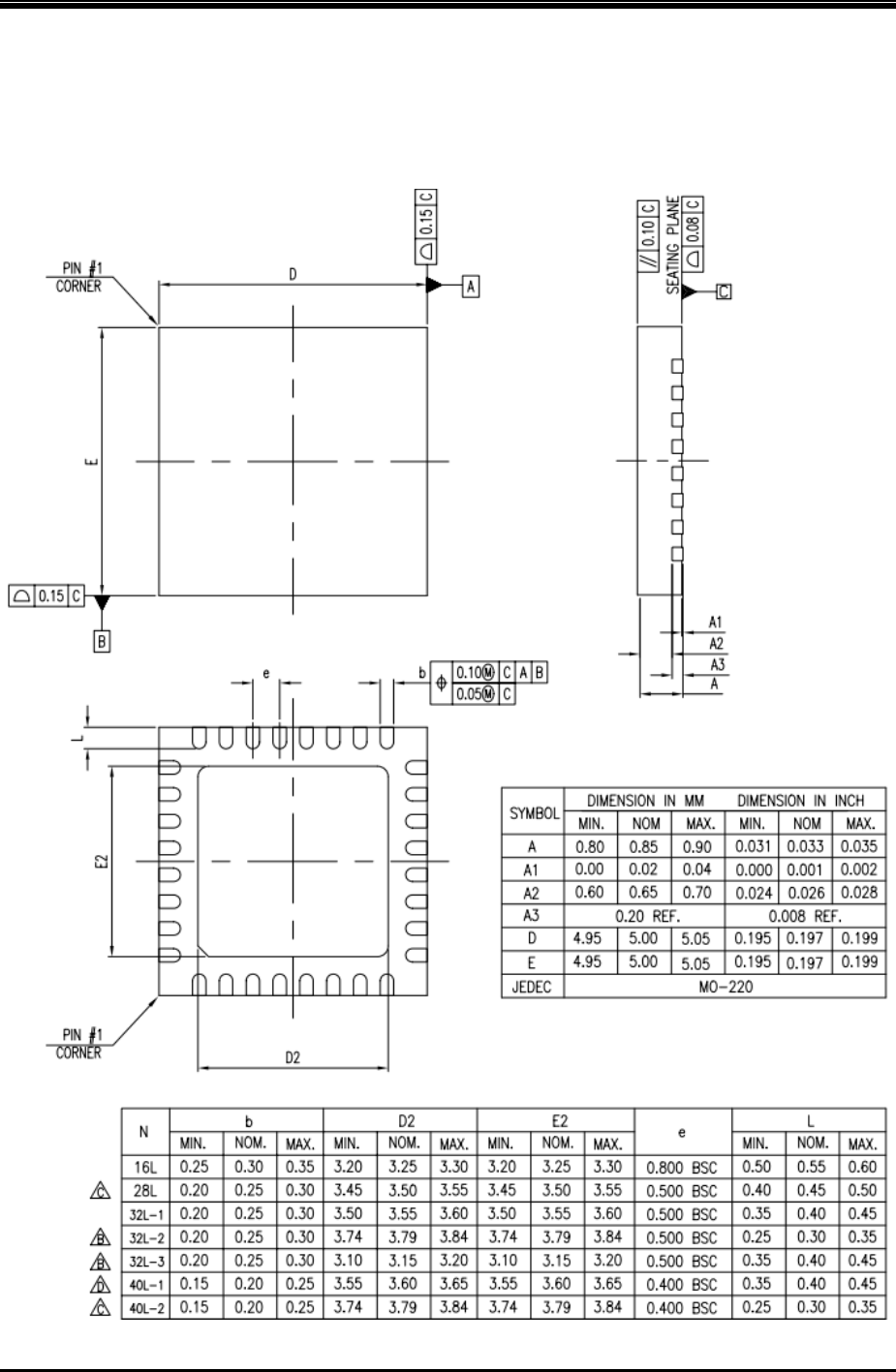
134 17.1 QFN32
Version 1.0.0
Copyright ©2015, www.appotech.com. All Rights Reserved.
17 Package Outline Dimensions
17.1 QFN32

17 Package Outline Dimensions 135
Version 1.0.0
Copyright ©2015, www.appotech.com. All Rights Reserved.
Figure 17-1 QFN32 Package Outline Dimension

17 Package Outline Dimensions i
Version 1.0.0
Copyright ©2015, www.appotech.com. All Rights Reserved.
Revision History
Date Version Comments Revised by
2015-10-23 0.0.1 Initial verison YX
2015-10-23 0.0.2 Modify Feature,delete IIC/IIS/SD…… CJ
2015-10-26 0.0.3 Modify and check GAO
2015-10-26 1.0.0 Release YX
FCC Warning Statement
This equipment has been tested and found to comply with the limits for a Class
B digital device, pursuant to part 15 of the FCC Rules. These limits are
designed to provide reasonable protection against harmful interference in a
residential installation. This equipment generates, uses and can radiate radio
frequency energy and, if not installed and used in accordance with the
instructions, may cause harmful interference to radio communications.
However, there is no guarantee that interference will not occur in a particular
installation. If this equipment does cause harmful interference to radio or
television reception, which can be determined by turning the equipment off and
on, the user is encouraged to try to correct the interference by one or more of
the following measures:
•Reorient or relocate the receiving antenna.
•Increase the separation between the equipment and receiver.
•Connect the equipment into an outlet on a circuit different from that to which
the receiver is connected.
•Consult the dealer or an experienced radio/TV technician for help.
Caution: Any changes or modifications to this device not explicitly approved by
manufacturer could void your authority to operate this equipment.
This device complies with part 15 of the FCC Rules. Operation is subject to the
following two conditions: (1) This device may not cause harmful interference,
and (2) this device must accept any interference received, including
interference that may cause undesired operation.
The device has been evaluated to meet general RF exposure requirement. The device
can be used in portable exposure condition without restriction.