Yorkville 3400 Users Manual
3400 to the manual 2b1c4d26-4522-9234-d56e-303018bd5c4c
2015-02-03
: Yorkville 3400-Users-Manual yorkville-3400-users-manual-474310 yorkville pdf
Open the PDF directly: View PDF ![]() .
.
Page Count: 25
- Cover
- Safety
- Service Manual Notes
- M1012A - The Input Board
- M1011A - Voltage Amplifiers and System Control
- Voltage Amplifier
- Circuit Description
- Shutdown Circuit
- M1002A - Current Amplifier Board
- Simplified Schematic
- Quiescent Condition
- The Second Tier
- Current Limit Protection Circuitry
- DC Protection
- EMS Circuit
- Fan Circuit
- Thermal Shutdown Circuit
- Identifying Defective Boards in the AP-3400
- Specifications
- Indentifying Defective Boards in the AP-3000 & AP-3400
- Parts List
- Schematics and Layouts
- Testing Repaired Circuit Board
- Quick Fix for M1002 and M1002A
- Wiring-AP3400CE230V-00-0v0
- Wiring-AP3400CE245V-00-0v0

SERVICE MANUAL
3
400
HIGH EFFICIENCY STEREO POWER AMPLIFIER
U.S.A.
Yorkville Sound Inc.
4625 Witmer Industrial Estate
Niagara Falls, New York
14305 USA
Voice: (716) 297-2920
Fax: (716) 297-3689
WORLD HEADQUARTERS
CANADA
Yorkville Sound
550 Granite Court
Pickering, Ontario
L1W-3Y8 CANADA
Voice: (905) 837-8481
Fax: (905) 837-8746
Quality and Innovation Since 1963
Printed in Canada
Manual-Service-AP3400-00-1v6.pdf
1
AUDIOPRO AP-3400 SERVICE MANUAL
M1012A “THE INPUT BOARD”
The input board processes the audio signal from the input jacks to the voltage amplifier board, (M1011A).
Each channel consists of a balanced gain stage, defeatable bass boost filter, and a preemphasis filter network.
The balanced input, (XLR Jack) and unbalanced input (phone jack) are wired in parallel to the input of a balanced
operational amplifier, (U1). The gain of this stage is 1.6 (4dB) balanced and 1.6 (4dB) unbalanced. Resistors R1, R5
along with capacitors C1 and C2 form a radio interference elimination filter.
Switch S1 selects a flat or bass boosted frequency response. The bass boost filter provides a 20Hz high pass, high Q
filter response with a +4dB peak at 55Hz. The filter consists of a tee network on the input of U1A along with R9, R10,
R11, C5 and C6. The gain is 1 (0dB) in the passband, (above 100Hz).
Operational amplifier U3B is a high pass shelving filter with a +2dB shelf above 20KHz. This filter provides the pre-
emphasis required to obtain a flat frequency response (to 20KHz) on the power amplifier output at full power.
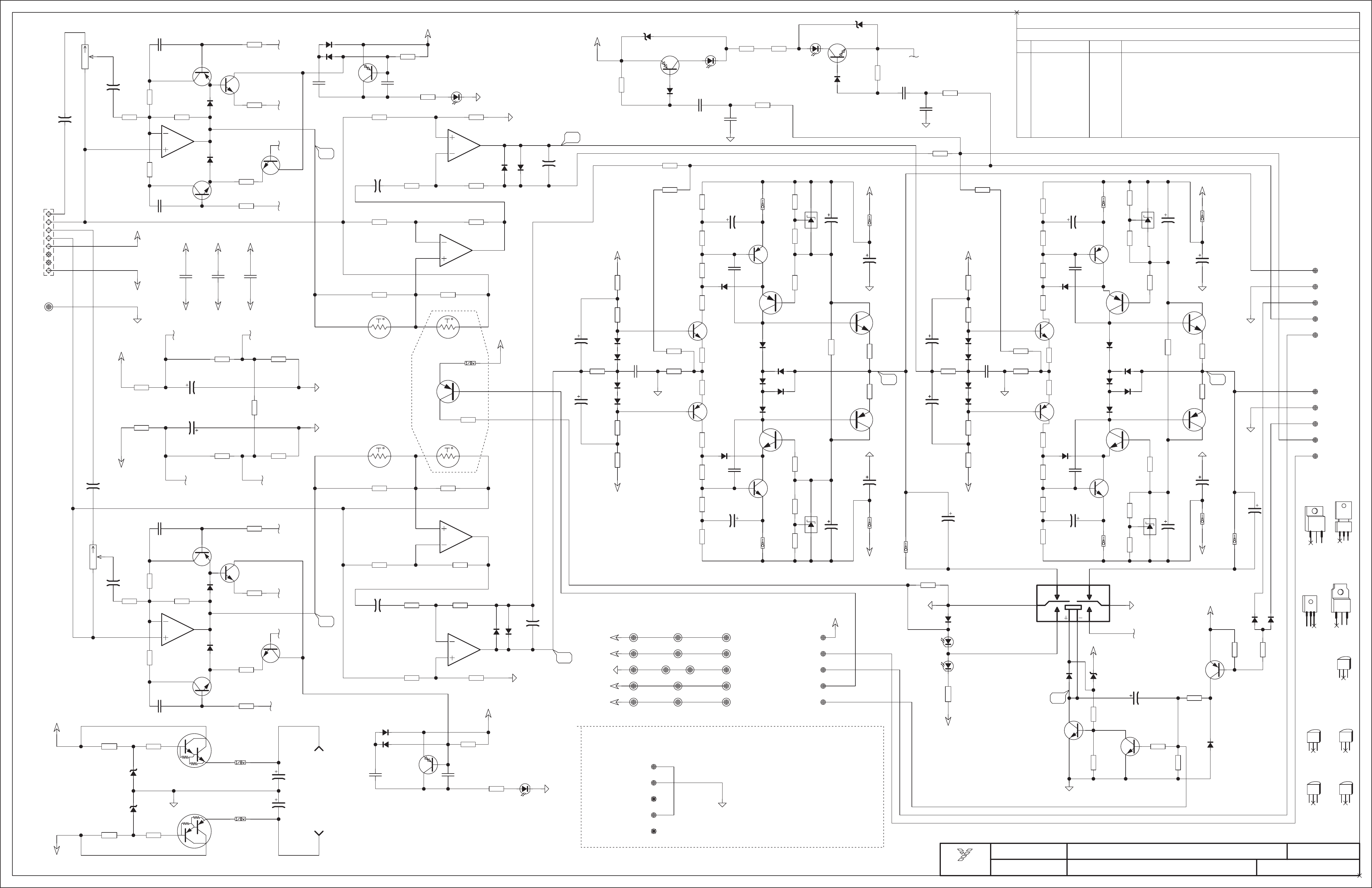
M1011A "VOLTAGE AMPLIFIERS AND SYSTEM CONTROL"
This board contains:
•Voltage amplifiers to drive the current amplifiers on the M1002A boards.
•The front panel volume control circuitry.
•The EMS control system with its associated circuits: Pre clipping and line current sensing heater circuits.
•Clip and activity LED's. Driver circuitry for the amplifier disable relay (used during amplifier turn on, turn off,
thermal shutdown and current limiting).
Circuit Explanation:
Refer to the schematic of M1011A as the sections of the circuit are explained.
The audio signal enters the board from M1012A through connector MS4. The two channels are marked "L" and "R"
for left and right. The signals are to be considered as differential sources and therefore are marked as L+, L-,R+ and
R-. Since the left channel has the same topology as the right channel we will only look at the left channel.
The signal ("L+") at the terminal block (MS4) passes through the front panel level control (P1) and the desired level
enters the inverting input of U1.
Op amp U1 is an inverting amplifier with a set gain of 2.40 (7.6dB). Built around U1 is a dual purpose circuit controlled
by a voltage divider consisting of R15, R16, R17, R18, R19, R20 and R21. The voltage divider sets two reference
levels, (HDRM & CLP). Reference voltage levels vary with the voltage levels on the +/-144VDC supply rails. As the
amplifier?s output is loaded, the supply rails voltage decreases and so do the reference levels.
Transistors Q1, Q3 the surrounding resistors provide a pre-clipping function that tracks the supply rails through the
HDRM voltage reference and clips the audio signal at approximately 11.2V pk. The clip LED indicator circuit is
connected through D1 and D2 to the output of U1, The bases of Q2 and Q4 are connected to the “CLP” reference
voltage, and when the peak output voltage of U1 (+/-Vp) is enough to forward bias the transistor junctions, Q2 or Q4
will trigger the clip led circuit (Q5), and illuminate the clip LED.
The audio signal on the output of U1 enters U3 through R43 and RV1. Under normal operating conditions the gain of
U3 is 1(0dB). The signal then passes through U2 to the voltage amplifier.
The exclamation point within an equilatereal
triangle is intended to alert the user to the
presence of important operating and
maintenance (servicing) instructions in the
literature accompanying the appliance.
Le point d’exclamation à l’intérieur d’un triangle équilatéral
est prévu pour alerter l’utilisateur de la présence
d’instructions importantes dans la littérature accompag-
nant l’appareil en ce qui concerne l’opération et la
maintenance de cet appareil.
This lightning flash with arrowhead symbol,
within an equilateral triangle, is intended to alert
the user to the presence of uninsulated
“dangerous voltage” within the product’s enclosure
that may be of sufficient magnitude to constitute a risk of
electric shock to persons.
Ce symbole d’éclair avec tête de flèche dans un triangle
équilatéral est prévu pour alerter l’utilisateur de la présence
d’un « voltage dangereux » non-isolé à proximité de l’enceinte
du produit qui pourrait être d’ampleur suffisante pour présenter
un risque de choque électrique.
IMPORTANT SAFETY INSTRUCTIONS
safety-4v5.eps • April 3/2007
CAUTION: TO REDUCE THE RISK OF ELECTRIC
SHOCK, DO NOT REMOVE COVER (OR BACK).
NO USER SERVICEABLE PARTS INSIDE.
REFER SERVICING TO QUALIFIED
SERVICE PERSONNEL.
FOLLOW ALL INSTRUCTIONS SUIVEZ TOUTES LES INSTRUCTIONS
Instructions pertaining to a risk of fire,
electric shock, or injury to a person
Read Instructions: The Owner’s Manual should be read and
understood before operation of your unit. Please, save these instruc-
tions for future reference and heed all warnings.
Clean only with dry cloth.
Packaging: Keep the box and packaging materials, in case the unit
needs to be returned for service.
Warning: To reduce the risk or fire or electric shock, do not expose
this apparatus to rain or moisture. Do not use this apparatus near water!
Warning: When using electric products, basic precautions should
always be followed, including the following:
Power Sources
Your unit should be connected to a power source only of the voltage specified in the
owners manual or as marked on the unit. This unit has a polarized plug. Do not use
with an extension cord or receptacle unless the plug can be fully inserted. Precau-
tions should be taken so that the grounding scheme on the unit is not defeated.
Hazards
Do not place this product on an unstable cart, stand, tripod, bracket or table. The
product may fall, causing serious personal injury and serious damage to the product.
Use only with cart, stand, tripod, bracket, or table recommended by the manufacturer
or sold with the product. Follow the manufacturer’s instructions when installing the
product and use mounting accessories recommended by the manufacturer.
The apparatus should not be exposed to dripping or splashing water; no objects
filled with liquids should be placed on the apparatus.
Terminals marked with the “lightning bolt” are hazardous live; the external wiring
connected to these terminals require installation by an instructed person or the use of
ready made leads or cords.
Ensure that proper ventilation is provided around the appliance. Do not install near
any heat sources such as radiators, heat registers, stoves, or other apparatus
(including amplifiers) that produce heat.
No naked flame sources, such as lighted candles, should be placed on the apparatus.
Power Cord
Do not defeat the safety purpose of the polarized or grounding-type plug. A polarized plug
has two blades with one wider than the other. A grounding type plug has two blades and a
third grounding prong. The wide blade or the third prong are provided for your safety. If the
provided plug does not fit into your outlet, consult an electrician for replacement of the
obsolete outlet. The AC supply cord should be routed so that it is unlikely that it will be
damaged. If the AC supply cord is damaged DO NOT OPERATE THE UNIT.
Unplug this apparatus during lightning storms or when unused for long periods of time.
Service
The unit should be serviced only by qualified service personnel.
AVIS: AFIN DE REDUIRE LES RISQUE DE CHOC
ELECTRIQUE, N’ENLEVEZ PAS LE COUVERT (OU LE
PANNEAU ARRIERE) NE CONTIENT AUCUNE PIECE
REPARABLE PAR L’UTILISATEUR.
CONSULTEZ UN TECHNICIEN QUALIFIE
POUR L’ENTRETIENT
Instructions relatives au risque de feu,
choc électrique, ou blessures aux personnes
Veuillez Lire le Manuel: Il contient des informations qui devraient
êtres comprises avant l’opération de votre appareil. Conservez.
Gardez S.V.P. ces instructions pour consultations ultérieures et
observez tous les avertissements.
Nettoyez seulement avec le tissu sec.
Emballage: Conservez la boite au cas ou l’appareil devait être
retourner pour réparation.
Avertissement: Pour réduire le risque de feu ou la décharge
électrique, n'exposez pas cet appareil à la pluie ou à l'humidité.
N’utilisez pas cet appareil près de l’eau!
Attention: Lors de l’utilisation de produits électrique, assurez-vous
d’adhérer à des précautions de bases incluant celle qui suivent:
Alimentation
L’appareil ne doit être branché qu’à une source d’alimentation correspondant au
voltage spécifié dans le manuel ou tel qu’indiqué sur l’appareil. Cet appareil est
équipé d’une prise d’alimentation polarisée. Ne pas utiliser cet appareil avec un
cordon de raccordement à moins qu’il soit possible d’insérer complètement les trois
lames. Des précautions doivent êtres prises afin d’eviter que le système de mise à la
terre de l’appareil ne soit désengagé.
Risque
Ne pas placer cet appareil sur un chariot, un support, un trépied ou une table instables.
L’appareil pourrait tomber et blesser quelqu’un ou subir des dommages importants.
Utiliser seulement un chariot, un support, un trépied ou une table recommandés par le
fabricant ou vendus avec le produit. Suivre les instructions du fabricant pour installer
l’appareil et utiliser les accessoires recommandés par le fabricant.
Il convient de ne pas placer sur l’appareil de sources de flammes nues, telles que
des bougies allumées.
L’appeil ne doit pas être exposé à des égouttements d’eau ou des éclaboussures
et qu’aucun objet rempli de liquide tel que des vases ne doit être placé sur l’appareil.
Assurez que lappareil est fourni de la propre ventilation. Ne procédez pas à
l’installation près de source de chaleur tels que radiateurs, registre de chaleur, fours
ou autres appareils (incluant les amplificateurs) qui produisent de la chaleur.
Les dispositifs marqués d’une symbole “d’éclair” sont des parties dangereuses
au toucher et que les câblages extérieurs connectés à ces dispositifs de
connection extérieure doivent être effectivés par un opérateur formé ou en utilisant
des cordons déjà préparés.
Cordon d’Alimentation
Ne pas enlever le dispositif de sécurité sur la prise polarisée ou la prise avec tige de
mise à la masse du cordon d’alimentation. Une prise polarisée dispose de deux
lames dont une plus large que l’autre. Une prise avec tige de mise à la masse
dispose de deux lames en plus d’une troisième tige qui connecte à la masse. La
lame plus large ou la tige de mise à la masse est prévu pour votre sécurité. La prise
murale est désuète si elle n’est pas conçue pour accepter ce type de prise avec
dispositif de sécurité. Dans ce cas, contactez un électricien pour faire remplacer la
prise murale. Évitez d’endommager le cordon d’alimentation. N’UTILISEZ PAS
L’APPAREIL si le cordon d’alimentation est endommagé.
Débranchez cet appareil durant les orages ou si inutilisé pendant de longues périodes.
Service
Consultez un technicien qualifié pour l’entretien de votre appareil.
S2125A
2
VOLTAGE AMPLIFIER:
The voltage amplifier amplifies the audio signal?s voltage from 4.8 volts peak (at the output of U2) to approximently
97v peak which is required to drive the current amplifier board M1002A. M1002A provides the current required for the
97v peak signal to drive 1200 watts into 4 ohms out of the binding posts.
Before the circuit is described in detail here is a quick rundown on the signal?s path through the voltage amplifier
stage. Refer to the schematic of M1011A. Let's consider that a positive going AC signal is present @ test point 3. The
positive going signal will turn on the positive side of the voltage amplifier. The signal at test point 3 turns on Q12
(through R40, D14 and D13). The collector of Q12 pulls down on the base of Q14, turns this transistor on further and
allows a greater current to flow out of Q14?s collector. This increase in current passes through Q15 and it?s collector to
emitter voltage drop decreases. The collector of Q15 now being more positive in voltage turns the base of Q18 on
causing an increase in Q18?s collector current resulting in test point 5 going positive.
As the positive side of the amplifier was turning on the negative side would have been turning off. This is how test
point 5 was able to move positive following the input signal. The reverse would hold true if a negative going signal was
present on the input of the voltage amplifier.
CIRCUIT DESCRIPTION:
The voltage amplifier is a mirrored image with circuitry connected to the positive power supply rail being identical (but
opposite polarity) to the circuitry connected to the negative power supply rail.
For this reason we will look in detail at the positive side of the amplifier.
The audio signal enters the voltage amplifier at test point 3. The signal passes through R40, D14 and D13 to the base
of Q12. Diodes D13 and D14 set up the DC bias on Q12 to approximately 0.6 mA.
The first voltage gain stage consists of Q12 along with the resistor chain on its collector and the emitter resistor (R44).
Transistor Q12 drives the base of Q14 through the resistor chain. A DC current of approximately 6 mA should flow
through the collector of Q14. The voltage drop across Q14 remains constant and is derived from the voltage drop
across the voltage reference Q20, resistor R58, and the base/emitter junction of Q15. This total voltage should equal
approximately 3 VDC. Transistor Q14 is the second gain stage and its output current flows through Q15. Transistor
Q15 is a common base stage with the collector driving the base of output buffer Q18.
Diode D17 is a clamping diode that prevents the maximum peak of the audio signal from coming within 4V of the 144
VDC rail. This is to prevent the output current amplifier (board M1002A) from going into saturation during clipping and
therefore having storage delay problems.
Transistor Q18 buffers the high impedance present on the collector of Q15. The output of the buffer provides a low
output impedance at test point 5 and is current limited to 25mA through the clamping action of D19, D20 and D23.
The signal at TP-5 drives the current amp board M1002A.
DC offset on the amplifier?s output is corrected by operational amplifier U2. The DC offset forms a current through
R54, R14 and is blocked by C5 giving a DC offset correction gain of -1.
The activity L.E.D. function is a simple charge pump circuit with a transistor that redirects a constant current path
through the activity L.E.D.
3
SHUTDOWN CIRCUIT:
The last circuit on board M1011A is the shutdown relay and its associated drive circuitry. The relay circuit has two
possible operating states.
1. Amplifier on under normal operating conditions.
2. Amplifier power switch has just been turned OFF/ON or the amplfier is in current limit protecting the amplifier?s
output or the amplifier has overheated.
CIRCUIT DESCRIPTION
Here is how the circuit accomplishes these functions. The relay?s normally closed contacts short the output of the
voltage amplifiers to ground when the power switch is off. When the power switch is turned on, the relay remains off
(normally closed) for about 6 seconds. C52 charges to 35V and results in Q37 turning off allowing Q36 to turn on. As
Q36 turns on, it connects the negative terminal of the relay?s coil (Pin 16) to ground energizing the relay and opening
the normally closed contacts.
If prolonged current limiting occurs on the amplifier?s output transistors then D50 or D51 (depending on which channel
is current limiting) will be forward biased turning on Q38 (from its off state). Now +144VDC appears on the collector of
Q38 and through R130 and R128 turn on Q37 therefore turning off Q36 by shorting its base emitter junction. Q36
turning off will turn the relay off and the normally closed contacts (off state) will short the outputs of the voltage
amplifiers to ground so as not to continuously stress the amplifier?s output transistors. A cycle now occurs. With the
voltage amplifiers now disabled there is no signal driving the output transistors (Q14 to Q28) on board M1002A.
The current limit circuit on M1002A turns off and D50 and/or D51 are not forward biased and Q38 turns off. Through
Q37 and Q36 the relay is turned back on and the voltage amplifiers are now active again, driving the output
transistors. If current limiting still occurs, then the same cycle will occur. If the cause of current limiting (low impedance
or short on the speaker output terminals) has been removed, then the amplifier will continue to operate normally.
The third operation that the relay provides is "overheat shutdown". If for some reason the fan cannot keep the
heatsinks in a safe operating temperature area then the fan control circuit (on board M1013A) will deliver through the
"kill" signal line a positive current to turn Q37 on and turn Q36 off to turn off the relay and disable the voltage
amplifiers. When the temperature of the amplifier has been cooled down by the fan, then the kill signal will disappear
and the relay circuit will turn on the relay to resume normal operation. Anytime the relay is in the "protect" mode (due
to the abnormal states) then contact pin 8 of the relay will illuminate LD5 (the protect LED on the front panel).
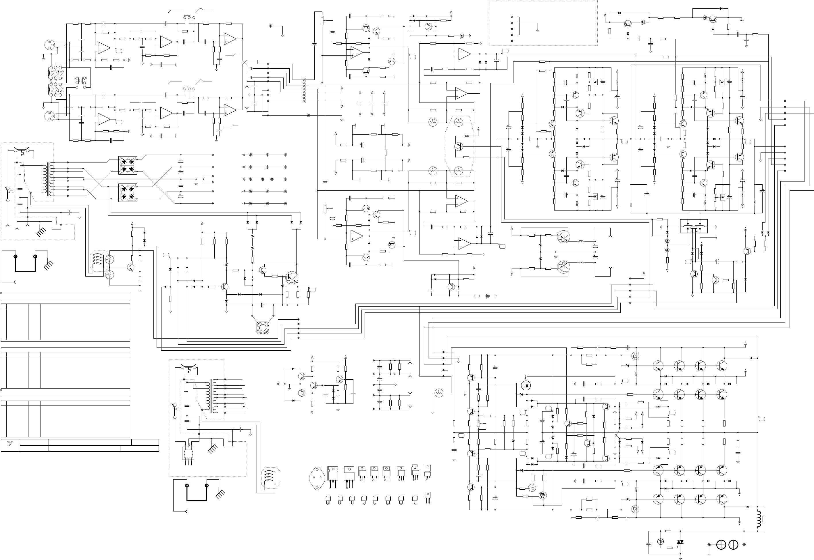
M1002A “CURRENT AMPLIFIER BOARD”
The current amplifier board (M1002A) receives a high voltage audio signal from voltage amplifier board (M1011A) and
provides the current drive necessary to drive speaker cabinets.
The current amplifier is a two tier complimentary output driver design controlled by a complimentary mos-fet stage.
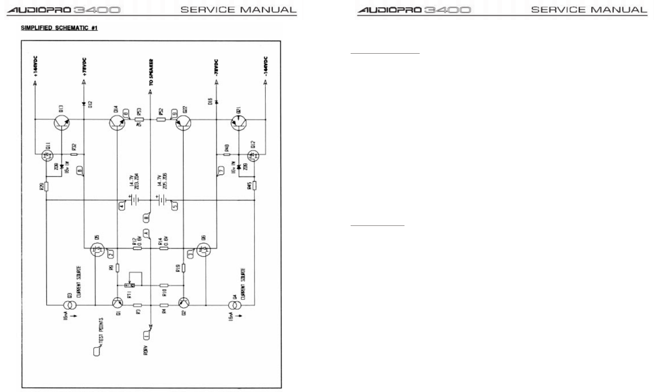
CIRCUIT DESCRIPTION - REFER TO THE SIMPLIFIED SCHEMATIC #1 ON THE FOLLOWING PAGE
4 5
QUIESCENT CONDITION:
This design is class A/B and therefore the output driver transistors must be forward biased to provide low crossover
distortion. In most class A/B designs, a diode chain or VBE multiplier is used to control the bias voltage and provide a
means of adjusting the bias. This design is different as there isn't a diode chain or VBE multiplier. For simplicity lets
consider only the positive side of the current amplifier, that is all parts between the positive power supply rails and the
audio signal output/input terminals. The negative side is the same as the positive, except for polarity changes.
To bias Q14, greater than 0.5V is needed from base to emitter, (or for simplicity from base to amplifier output). Points
A and B are at the same potential, so consider them to be connected. If this is true then 0.5V from test point 2 to the
amplifier output must appear across R12. There must be some way of developing this voltage across R12, and there
is using the mos-fet (Q5) driver along with local feedback.
Simplified schematic Fig. #1 shows the biasing circuit. The current needed to develop 0.5V across R12 comes from
the source of Q5. When the amplifier is first turned on the current source (Q3) turns on Q5 and current flows through
R12 developing a voltage. When this voltage approaches 0.5V Q1 turns on and robs current from the gate of Q5.
This causes Q5 to turn off until the reduced current flowing through Q5 maintains 0.5V across R12. Q1 will turn off
slightly causing Q5 to increase its source current. The circuit reaches a point of equilibrium with approximately 0.5V
across R12.
Because all output devices are not identical and base emitter voltages vary, some adjustment must be available to
slightly adjust the 0.5V across R12. This is accomplished with RT1. RT1 causes Q1 to turn on slightly more or less
resulting in Q5 turning on slightly more or less and therefore R12? s voltage will be slightly more or less than 0.5v. The
proper quiescent current adjustment is 4mV ( to be measured between test points 8 and 9).
THE SECOND TIER:
Refer to the simplified schematic Fig. #1 while reading the following text. One way of making an amplifier more
efficient is to vary the Power Supply Voltage on the collectors of the output transistors (Q14 & Q22). The lower the
voltage from collector to emitter, the lower the device dissipation. During quiescent conditions, there is 78VDC on the
collectors of output transistors Q14 and Q22. The peak AC voltage that can appear on the amplifier's output is
approximately 132V peak. How can an output transistor deliver a 132V peak when its collector is only at 78VDC? It
can if its collector is pulled up to 144VDC as the output signal's peak rises above 78VDC. (refer to Fig. #2). The
second tier voltage must remain above the amplifier's output voltage by amount Vm. Therefore the circuitry controlling
the second tier voltage must increase the tier voltage before the amplifier's output voltage reaches 78VDC. This
leading voltage is necessary to compensate for time lag of the second tier circuit during fast rising amplifier output
signals.
6
The voltage between the
amplifier?s output and test point
4 is approximately 14.7VDC
derived from the voltage drop
across ZD3 @ ZD4. We call this
voltage the “floating battery”
because it floats on top of the
output audio signal with point 4
always being 14.7VDC greater
than the peak of the output
signal. Point 4 drives the gate of
mos-fet Q11. Q11 controls the
transistors of the upper tier. As
Q11 turns on it's source foward
biases the base of Q13 and Q13
pulls the collector of Q14
towards the 144 volt rail. The
gate to source voltage needed to
turn on Q11 is approximately 3.5
volts. When the peak output
signal is about 67vp (55v-(14.7v-
3.5v)) then Q11 will start to turn on the second tier. The second tier voltage will remain about 11 volts (Vm) above the
peak of the output signal to the point of clipping where this voltage is reduced to about 4 volts. Zener ZD8 protects the
gate source junction of Q11 and also provides a current path through R29 for the “floating battery”.
Current Limit Protection Circuitry
To have an amplifier drive 3000 watts into practically any combination of speaker cabinets and know what is a safe
load and what is not is a very difficult task. An extensive amount of time was spent on the current limit circuitry so that
it may simulate the safe operating area of the output transistors (SOAR curve). No matter how reactive the load may
be the phase shift that it presents, along with it's resistive component is used to set the output current limit of the
output transistor stage.
Refer to the schematic of board M1002A while reading the following text. The current limit circuitry is a mirrored image
with circuitry connected to the positive power supply rail being identical (but opposite polarity) to the circuitry
connected to the negative power supply rail. For this reason we will look at the positive side of the circuitry.
Transistor Q9 measures the peak current flowing through resistor R53. The voltage across R53 (as a result of the
current flowing through it) is scaled down by R55, R35, R36, R37, D7 and D11- these parts make up the safe
operating area along with the time constants of C26, R34, C12 and R26. Fig. #3 shows a waveform of the current that
passes through R52 and R53 when the output of the amplifier is shorted to ground. This can only be seen by using an
oscilloscope to measure differentially across R52 and R53. The conditions of the measurement are contained on the
diagram. During current limit when Q9 turns on it reduces the voltage across R42. R42 is in series with a 16 volt zener
(ZD7) and is also in parallel with the junction of Q8. Q8 is normally saturated by the current that flows through R20,
ZD7, R42, and R22. When Q9 reduces the voltage across ZD9 and R42 to below 16.6 volts then Q8 turns off allowing
a charge to build up on C8 through resistors R24 and R25. If current limiting occurs for a long enough duration to
allow C8 to charge to 1.2 volts then Q7 will turn on tripping the relay circuit on board M1011A. As soon as the relay is
turned off the audio signal will be turned off at the voltage amplifiers and will remain off for about 5 seconds before the
relay turns on and allows the audio signal to pass through the amplifier. If a current limit condition is still present then
the whole cycle will occur again and repeat until the load conditions on the amplifier's output are safe for the amplifier.
When a safe load reappears the amplifier will automatically reset and drive that load (the speaker cabinet).
Subwoofers present large inductive loads to the amplifier and are driven at low frequencies where the large current
peaks must be tolerated for short periods of time. To accomodate this type of loading C26 and R34 are used to retard
the firing of Q9 at low frequencies.
7
DC Protection
If a DC voltage greater than 8 volts appears on the output of the amplifier for more than 200 milliseconds then triac
Q30 will turn on holding the output at ground potential. MBS4992 is a device that turns on at either + or - 8 volts DC.
NOTE:
Everytime you replace blown output transistors on a M1002A board
test the DC protection triac with the following circuit.
Conditions of test:
A. Pass a 100Hz 25v peak signal through the M1002A board under test with no load connected to the amplifier
output.
B. Connect points 1 and 2 as shown in the diagram. The amplifier should go into protect mode as the triac ( if
working) shorted the output of the amplifier to ground, and the amplifier goes into current limit.
C. Disconnect the triac test circuit and allow the amplifier to complete it?s protect cycle.
D. Reverse connections 1 to 2 and 2 to 1 and test again. The same results as in B) should be observed if the triac is
working.
Only test the triac for one protect cycle as prolonged testing will heat the triac to a high temperature.
8
EMS Circuit
The Energy Management System circuit only applies to North American line voltage products. A North American AC
receptacle can provide 1850 watts before the wall breaker would trip, but how can a amplifier provide 2 x 1200 watts
out when only 1850 watts is avaliable out of the AC receptacle? A sinewave source connected to the amplifier driving
the amplfier to full power output will cause the circuit breaker on the amplifier to trip. Music driving the amplfier to
clipping can be equal an average power output between 12 and 30 percent of the amplifier?s maximum capable power
output. Under this condition less than 12 ampheres of current is drawn from the AC line. Some synthesized music
may go beyond the 12 to 30 percent level and make the amplfier draw more than 12 amperes from the AC line. If this
occurs the coil on board M1013A heats up to the point where through the heating of thermistor RV5, Q32 sinks
current through R109. On board M1011A Q11 starts conducting through the connection to R109. Q11 heats
thermistors RV2 and RV4 attenuating the audio signal going to each amplfier channel, thus decreasing the current
drawn from the AC line to the point where less than 12 ampheres is being drawn.
Fan Circuit
Looking at the schematic to
board M1013A, here is a quick
explaination of the fan control
circuit. There is a thermistor on
each M1002A board. When the
amplifier is first turned on, Q33
is saturated sinking the current
source through ZD10. As either
negative temperature coefficient
thermistor begins to heat up,
more current flows through D38
or D39 decreasing the conductor
of Q33 until the increasing VCE
of Q33 is enough to turn on Q34
and Q35. Further heating of the
thermistor causes an increasing
of Q33?s collector to emitter
voltage. Q34 and Q35 are a
common emitter stage with Q35
providing the drive current for the fan. To lower the dissipation of Q35, D42, D43, ZD12, ZD13 and R118 turn off Q35
when the full wave rectified voltage present of the collector of Q35 reaches approximently 50V by robbing current from
the base of Q34. The maximum fan voltage is 20.5 VDC. ZD14 and R120, R121 and R122 provide a current limiting
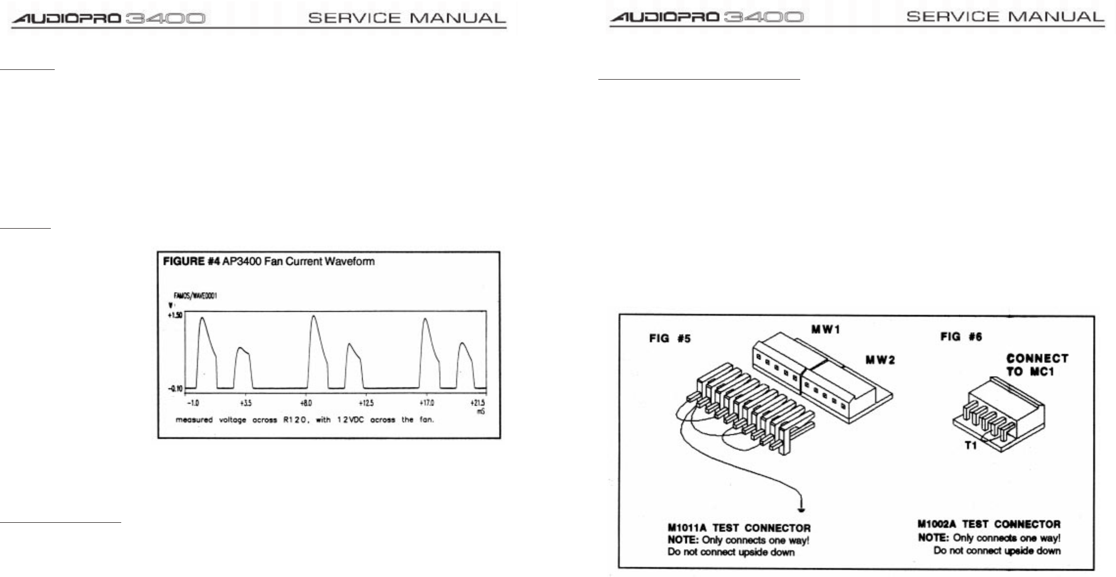
function. Figure #4 shows the current throught these resistors when there is 12VDC across the fan.
Thermal Shutdown Circuit
Test point 7 in the fan circuit is the measuring point for the shutdown voltage. As the temperature sensing thermistors that
control the fan circuit heat up the voltage on test point 7 rises until at 85 degrees celcius on the M1002A heatsinks the
voltage on test point 7 reaches 34.5 VDC and the amplifier must be shutdown to protect the output power transistors. ZD15
and D47 become forward biased and through the kill connection to board M1011A, Q37 on M1011A turns on turning the
relay off and muting the audio signal. After the amplifier cools down the kill voltage will decrease FIGURE #4 AP3400 Fan
Current Waveform until Q37 turns off turning the relay back on enabling the amplifier.
9
Identifying Defective Boards in the AP-3400
STEP 1: VISUAL INSPECTION OF FRONT PANEL AND FAN
A. Check to see whether the green power LED is lit. If not, the amplifier has a power supply (M1013A board),
transformer, A.C. switch or line cord problem.
B. If the red protect LED stays on or samples off and on, this usually indicates a problem with one or both of the
M1002A current amplifier modules and possibly damage to the M1011A voltage amplifier board. Check for
misaligned pin connections or see if the ribbon cables have been cut or pinched through their insulation.
C. The fan running at full speed on power up usually indicates a problem with the fan circuitry on the M1013A board,
but it can also be caused by M1011A circuit problems. Erractic fan behaviour can be caused by damaged
thermistors located under the M1002A heatsinks.
D. No output on either or both channels can be caused by intermittent push switches at the input.
STEP 2: VISUAL INSPECTION OF INTERNAL CHASSIS
A. a) After removing the lid, look for any signs of smoke, charring or burnt components. If the M1002A boards have
such damage there may be some damage to the M1011A voltage amp board in the form of blown ICs, or possibly
open or shorted diodes, LED?s, resistors, transistors or capacitors. Exploded electrolytic capacitors indicate you
have major repairs to the M1002A, M1011A and M1013A boards.

10
STEP 3: POWER UP PROCEDURE WITHOUT M1002A BOARDS
It is extremely important that you never power up an AP3400 with the interconnecting cablesbetween the circuit
boards not connected.
Time and possible further damage will be reduced if you test M1011A and M1002A boards separately. To do this you
must use the M1011A and M1002A test connecters. These are shown in figures #5 and #6. These can be made if the
Molex connector parts are available or order them from the Yorkville Service Parts Dept. With the test connectors
connected to every board, slowly variac up the line AC voltage.
NOTE:
It may be simplier to remove the power supply connections to M1002A boards not being troubleshooted to
reduce the possibility of further damage. With the M1011A test connector connected, a sinewave can be passed
through the board and be seen on test points 5 and 6. With the M1002 Atest connector installed, static DC
measurements can be made. A slight DC offset may be present on the board?s output as there will not be any DC
correcting feedback.
STEP 4: DISMANTLING AND REASSEMBLY PRECAUTIONS
A. When removing power supply wires or resoldering wires to eyelets on the M1011A board, double check that there
are no solder bridges or icicles bridging traces or other eyelets. Failure to do so will result in the destruction of
newly installed boards as well as other boards in the unit. Also make sure wire color codes are correctly oriented
in their proper eyelets, and be careful that ribbon cables don?t get pinched or cut under the M1011A board.
B. When reinstalling M1002A boards, make sure the output wires, i.e. the red and yellow signal and black ground
wires, are not reversed. If either or both channels are reversed, the amp will stay in protect mode with the red
protect LED staying on or sampling on and off.
11
SPECIFICATIONS
POWER
• All values are in WATTS at 1KHz, except FTC 20Hz-20KHz.
• Measurements made with regulated 120 VAC sine wave at line cord.
• All values are rounded down to the nearest 25 watts
BURST AVERAGE
Measured as a 2 cycle burst at 1KHz, 8:1 duty. (Continuous measurements may require line currents >15 Amps).
ONE CHANNEL DRIVEN (WATTS).
LOAD CONT. AVG. BURST AVG. PEAK INSTANT FTC 20-20KHz
8 ohms 900 1250 3000 800
4 ohms 1500 2250 6000 1200
BOTH CHANNELS DRIVEN (WATTS).
LOAD CONT. AVG. BURST AVG. PEAK INSTANT FTC 20-20KHz
8 ohms 750 1200 3000 650
4 ohms 1200 2175 6000 950
BRIDGED (WATTS)
LOAD CONT. AVG. BURST AVG. PEAK INSTANT FTC 20-20KHz
16 ohms 1500 2400 6000 1300
8 ohms 2400 4350 12000 1900
THD DISTORTION
LOAD AT 1KHz 20Hz - 20KHz
8 ohms <0.003 % <0.04 %
4 ohms <0.004% <0.05 %
CROSSTALK: -75 dB below full power at 1KHz
-60 dB below full power, 20Hz - 20KHz
INPUT IMPEDANCE: 20K ohms balanced, 10 Kohms unbalanced
INPUT SENSITIVITY: 1.4 VRMS sine wave = full power (36 dB gain).
FREQUENCY RESPONSE: Within 1dB, 20Hz to 20KHz (50Hz boost sw out)
HUM AND NOISE: -105 dB below max output RMS voltage, unweighted
DC OFFSET: less than 25 millivolts
PROTECTION: fully protected, DC, LOAD and THERMAL
COOLING: interleaved heatsink with DC servo controlled fan
SLEW RATE: Power amp: 30 V/usec, 60 V/usec in bridged mode
(rise time limited to 18 V/usec by input filter).
DAMPING FACTOR: >500, 20Hz - 400Hz, into 8 ohms
MAX OUTPUT CURRENT: 100 amperes for 10 milliseconds, 50 amperes continuous
TURN ON/OFF: < 15 milliwatts / seconds, 0.5 Wpk (1s on delay).
EFFICIENCY: Better than 75% at full power into 4 ohms
WEIGHT: 42 pounds 17.75 Kilograms
SIZE: 3.5" x 19" x 15.75" (front panel to binding posts)
POWER SUPPLY: Toroidal transformer and combination
power switch/circuit breaker
POWER COMSUMPTION: Will not exceed 13.5 Amps under actual conditions
Identifying Defective Boards in the AP-3000 & AP-3400
Please note: All boards used in the AP-3400 are designated with an `A' suffix (e.g. M1002A) and
use bright red solder mask
STEP 1: VISUAL INSPECTION OF FRONT PANEL AND FAN
a) Check to see whether the green power LED is lit. If not, the amplifier has a power supply (M1013
board), transformer, A.C. switch or line cord problem.
b) If the red protect LED stays on or samples off and on, this usually indicates a problem with one or both
of the M1002 current amplifier modules and possibly damage to the M1012 voltage amplifier board.
Note: Any of the Molex cables from the M1011 circuit board to the M1012 input board as well as the
M1002 current amplifiers can cause the protect LED to stay on or sample on and off. Check for
misaligned pin connections or see if the ribbon cables have been cut or pinched through their insulation.
c) The fan running at full speed on power up usually indicates a problem with the fan circuitry on the
M1013 board, but it can also be caused by M1011 circuit problems. Erratic fan behaviour can be caused
by damaged thermistors located under the M1002 heat sinks.
d) No output on either or both channels can be caused by intermittent push switches at the input.
STEP 2: VISUAL INSPECTION OF INTERNAL CHASSIS
a) After removing the lid, look for any signs of smoke, charring or burnt components. If the M1002
boards have such damage, the M1011, M1012 and M1013 boards may also be damaged even if there is
no similar charring on their components. At the least, there will be some damage to the M1011 voltage
amp board in the form of blown ICs, or possibly open or shorted diodes, LEDs, resistors, transistors or
capacitors. Exploded electrolytic capacitors indicate you have
major
repairs to the M1002, M1011 and
M1013 boards.
STEP 3: POWER UP PROCEDURE WITHOUT M1002 BOARDS
It is
extremely important
that you never power up an AP-3000 or AP-3400 without following the
procedure located on the M1011 schematic highlighted within the box drawn in dashed lines. Failure to do
so will possibly result in damaging a good board. This procedure should only be done on a no load
scoped output to insure the rest of the circuit boards are working before installing new or repaired M1011
modules. The output of a fully operational M1011 will give a 70V peak to peak sinusoidal (undistorted)
wave form when a patch plug is attached at Pin #1. If the wave form is distorted or non- existent, or there
is DC offset, do not attempt to connect any M1002 module to the M1011 or you will immediately destroy
the new or repaired M1002 and will also cause more damage to the rest of the amplifier.
Note: M1002?s
power supply wires (red, yellow, white, blue and black) must be removed as well as the
input Molex ribbon to the M1002 when attempting to power up an M1011.
STEP 4: DISMANTLING AND REASSEMBLY PRECAUTIONS
a) When removing power supply wires or resoldering wires to eyelets on the M1011 board, double check
that there are no solder bridges or icicles bridging traces or other eyelets. Failure to do so will result in the
destruction of newly installed boards as well as other boards in the unit. Also make sure wire color codes
are correctly oriented in their proper eyelets, and be careful that ribbon cables don?t get pinched or cut
under the M1011 boards as this will result in shut down into the protect mode or even destruction of more
boards.
b) When reinstalling M1002 boards, make sure the output wires, i.e. the red and yellow signal and black
ground wires, are not reversed. If either channels or both are reversed, the amp will stay in protect mode
with the red LED staying on or sampling on and off.
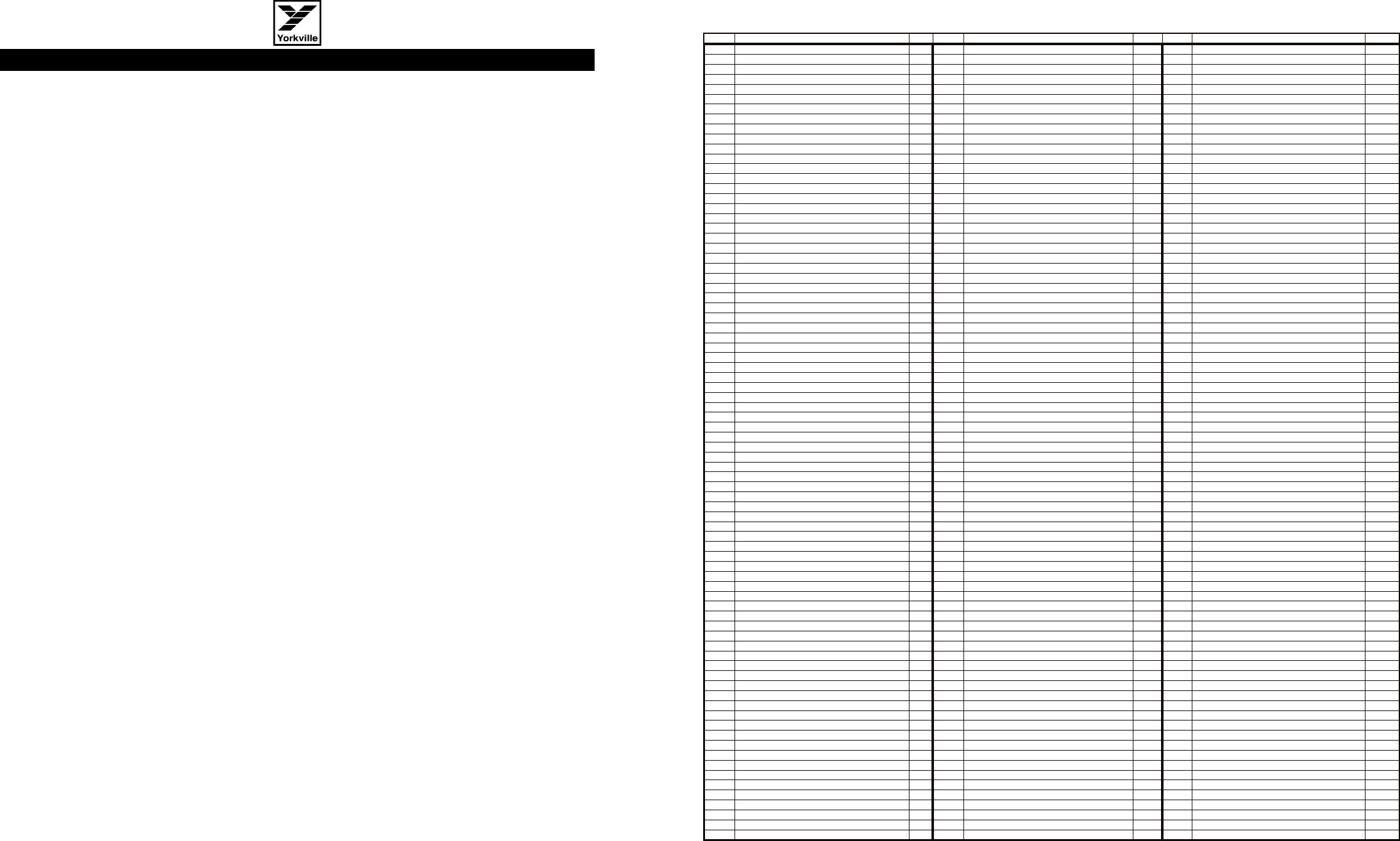
AP3400 Parts List 10/28/98
YS # Description Qty. YS # Description Qty. YS # Description Qty.
6410 GREEN 3MM LED 1V7 5MA BULK BRT CLR 3 5621 470U 63V 20%CAP RADIAL ELECT BULK 1 4854 1/4W 1K2 5% T&R RES 2
6411 RED 3MM LED 1V9 5MA BULK BRIGHT 3 5892 6800U 80V 10%CAP RADIAL ELECT BULK 8 4624 1/2W 1K5 5% T&R RES 1
6419 BRIDGE 35A 400V WIRE LEAD GI3504 2 4522 4K7 TRIM POT 2 4824 1/4W 1K5 5% T&R RES 12
6425 BAV21 200V 0A25 DIODE T&R 6 4400 _10K 25A-AUD/DETENT STYLE"P15"16MM 2 4847 1/4W 2K2 5% T&R RES 2
6438 1N4004 400V 1A0 DIODE T&R 10 3590 12.0 AMP SWITCH BREAKER WHITE 1 4804 1/4W 3K 5% T&R RES 8
6825 1N4148 75V 0A45 DIODE T&R 71 3822 500NH COIL 18AWG 0R000 AIR CORE 1 6124 1/4W 3K 5%MINI T&R RES 2
6934 MR854 400V 3A0 DIODE FAST RECOV 24 3820 4UH COIL 14AWG ZOBEL HORIZONTAL 2 4744 5.0W 3K6 5% BLK RES 8
6439 1N5225B 3V0 0W5 ZENER 5% T&R 4 3464 WIRE TO BOARD CRIMP 18-24 AWGT/LEAD 2 4827 1/4W 4K7 5% T&R RES 7
6440 1N750ARL 4V7 0W5 ZENER 5% T&R 5 3465 WIRE TO BOARD CRIMP 16-18 AWG TIN 4 4982 1/4W 4K7 5%MINI T&R RES 4
6459 1N4732A 4V7 1W0 ZENER 5% T&R 2 3486 CLIP 250X032 22-18AWG DISCO-LOK 14 4778 1/4W 5K36 1% T&R RES 2
6461 1N5240BRL 10V0 0W5 ZENER 5% T&R 1 3489 CLIP 250X032 18-22AWG DISCO/INSL 2 4862 1/4W 5K6 5% T&R RES 2
6450 1N5242B 12V0 0W5 ZENER 5% T&R 4 3490 CLIP 250X032 14-16AWG DISCO/INSL 1 4887 1/4W 7K5 5% T&R RES 11
6822 1N4745A 16V0 1W0 ZENER 5% T&R 4 3682 250 MALE PCB TAB BULK ON CATRIGE 14 4990 1/4W 8K2 5%MINI T&R RES 2
6824 1N5246B 16V0 0W5 ZENER 5% T&R 4 3447 DUAL BINDING POST TPP3 2 4800 1/4W 10K0 1% T&R RES 20
6432 1N5248B 18V0 0W5 ZENER 5% T&R 2 3498 M203-02 PLAIN PC MNT JK SKT 2 4829 1/4W 10K 5% T&R RES 2
6465 1N5250B 20V0 0W5 ZENER 5% T&R 4 3660 FEMALE PC MOUNT XLR NTRX.NC3FPR-H-O 2 4775 1/4W 14K0 1% T&R RES 5
6433 1N5257B 33V0 0W5 ZENER 5% T&R 3 3451 0.089 OD SMALL EYELET ELECTROPLATED 18 4630 1/2W 15K 5% T&R RES 10
5101 BC550C TO92 NPN TRANS. T&R 19 3542 SE44 LARGE EYELET TIN-PLATED BRASS 23 4830 1/4W 15K 5% T&R RES 5
5102 BC560C TO92 PNP TRANS. T&R 10 3630 FAN GUARD METAL 80MM CHROME 1 4771 1/4W 17K8 1% T&R RES 11
5103 MPSA06 TO92 NPN TRANS. T&R 1 3860 FAN 80MM X 80MM 40CFM 12VDC 1 6125 1/4W 18K 5%MINI T&R RES 2
5107 2N5551 TO92 NPN TRANS. T&R 5 3692 HEATSINK THERMALOY 6079-PB 5 4885 1/4W 20K 5% T&R RES 4
5113 MPSA42 TO92 NPN TRANS T&R 4 3893 AAVID HEATSINK 5811B 2 4777 1/4W 21K5 1% T&R RES 2
5114 MPSA92 TO92 PNP TRANS T&R 5 3894 AAVID 5972-B H/S W/TAB B.O. 4 4832 1/4W 22K 5% T&R RES 1
6854 2N6517 TO92 NPN TRANS. 2 3501 B52200F006 COMP WASH #4 SMALL 13 4833 1/4W 27K 5% T&R RES 6
5105 MPSA13 TO92 NPN DARLINGTONT&R 1 3750 VINYL CAP SC 0.500 BLACK 1/2" 1 4840 1/4W 33K 5% T&R RES 6
5106 MPSA63 TO92 PNP DARLINGTONT&R 3 3789 TERMINAL STRIP (BEAU INTERCONNECT) 1 4868 1/4W 36K 5% T&R RES 2
5123 NJM431L TO92 SHUNT REG T&R2V 4 3806 RECTANGULAR WASHER FOR TRANS SUPPR
T
1 4908 1/4W 45K3 1% T&R RES 1
6456 BF872 TO202 PNP TRANS. 1 8682 #4 TEFLON WASHER .125ID .281OD .031 1 4834 1/4W 47K 5% T&R RES 8
6873 MJE340 TO126 NPN TRANS 2 8498 6-32 X 3/8 STEEL PEM STUD 4 4836 1/4W 68K 5% T&R RES 6
6874 MJE350 TO126 PNP TRANS. 2 8499 6-32X1 STEEL PEM STUD 7 4772 1/4W 82K5 1% T&R RES 6
6891 TIP50 TO220 NPN TRANS 2 3795 #8 GROUND LUG ZIERICK 505-169 3 4898 1/4W 91K 5% T&R RES 4
6893 MJE5730 TO220 PNP TRANS 2 3468 8? 3/16 SJT AC LINE CORD STRIP 17" 1 4838 1/4W 100K 5% T&R RES 4
6779 MJH11018 TO218 NPN DARLINGTON 1 3821 HEYCO #1200 STRAIN RELIEF 1 4776 1/4W 113K 1% T&R RES 2
6911 BDX54C TO220 PNP DARLINGTON 1 3521 SIDE ENTRY PCB CONN .156 8POS 1 4839 1/4W 150K 5% T&R RES 4
6912 BDX53C TO220 NPN DARLINGTON 1 3541 24 PIN BREAKAWAY 90 .156 0.333 4668 2.0W 220K 5%10MM BODY T&R RES 2
6752 MTP10N15L TO220 N CHAN MOSFET 2 3543 20 PIN BRKAWAY 90 LOCK .156 0.75 4841 1/4W 220K 5% T&R RES 3
6923 MTP2P50E TO220 P CHAN MOSFET 4 3593 PCB CONN 90 5 CIR .156 3 6126 1/4W 220K 5%MINI T&R RES 4
6924 MTW10N40E TO247 N CHAN MOSFET 2 8701 4-40 KEPS NUT ZINC 17 4843 1/4W 470K 5% T&R RES 4
6925 MTP8P20 O220 P CHAN MOSFET 2 8793 4-40 HEX NUT ZINC 6 6127 1/4W 470K 5%MINI T&R RES 2
6900 YS6900 (22) TO3 NPN TRANS. 16 8760 6-32 KEPS NUT TIN PLATED 64 4844 1/4W 1M 5% T&R RES 1
6927 YS6927 (23) TO3 PNP TRANS. 16 8800 6-32 KEPS NUT ZINC 28 4797 1/4W 1M2 5% T&R RES 1
6840 MC33078P IC DUAL OP AMP 5 8854 6-32 X 1/4 HEX NUT ZINC 6 4888 1/4W 4M7 5% T&R RES 2
6884 NE5532N IC DUAL OP AMP 1 8787 8-32 KEPS NUT ZINC 3 3699 RELAY 2C 01AMP DC48 ???MA PC-S 1
5190 MBS4992 TO92 8V5 DIAC T&R 2 8797 5/16-18 KEPS NUT SJ500 1 3594 9.5" 5C-24AWG RIBBON HEAVY DUT.100" 3
6444 MAC224-4 TO220 40A TRIAC 200V 2 3797 TO-247 THERMO CONDUCTIVE PAD 3 3595 17" 8C-24AWG RIBBON HEAVY DUT.100" 1
6477 100K 5% 1/4W THERMISTOR T&R 0.2 8 3815 TO3 PREGREASED MICA 56-03-2AP 32 8865 4-40 X 5/16 PAN PH MS SJ500 4
5401 _10P 500V 5%CAP T&R RAD CER.2"NPO 4 3846 TO220 MICA THERMAL CONDUCTOR 56359B 8 8742 4-40 X 3/8 PAN PH TAPTITE JS500 4
5404 _27P 100V 10%CAP T&R TUBULAR NPO 2 4597 22AWG STRAN TC WIR 19 8861 4-40 X 3/8 PAN PH MS SJ500 1
5408 _47P 100V 10%CAP T&R BEAD NPO 4 4599 22AWG SOLID SC WIR T&R 79 8741 4-40 X 1/2 PAN PH MS JS500 13
5410 100P 100V 10%CAP T&R BEAD NPO 4 5299 24AWG SOLID SC WIR RAD 43 8871 4-40 X 5/8 PAN PH MS SJ500 2
5412 220P 100V 10%CAP T&R BEAD NPO 2 4745 5.0W 0R1 5% BLK RES 12 8799 #6 X 1/4 PAN PH TYPE B JS500 2
5201 470P 100V 5%CAP T&R RAD CER.2"NPO 2 4749 5.0W 0R15 5% BLK RES 4 8801 6-32 X 3/8 PAN PH TAPTITE SJ500 1
5416 470P 50V 10%CAP T&R BEAD NPO 6 4974 1.0W 0R47 5%FLAME PROOF T&R RES 4 8829 6-32 X 3/8 FLAT PH TAPTITE BO#4 HEA 15
5816 680P 100V 5%CAP T&R RAD CER.2"NPO 2 4677 1/2W 1R 5% T&R RES 4 8747 6-32 X 1/2 HEX ND MS ZINC 16
5422 __1N 50V 10%CAP T&R BEAD NPO 2 4877 1/4W 1R 5% T&R RES 2 8761 6-32 X 1/2 PAN PHIL MS ZINC CLEAR 64
5273 __1N5 200V 5%CAP T&R RAD CER.2"NPO 2 4973 1.0W 1R 5%FLAME PROOF T&R RES 4 8806 6-32 X 1/2 PAN PH TAPTITE SJ500 2
5427 __2N2 500V 10%CAP T&R RAD CER.2" YB 4 4688 1/2W 2R2 5% T&R RES 7 8802 8-32 X 3/8 PAN QUAD TPTTE SJ500 #6H 7
6451 __4N7 250V 20%CAP AC Y ONLY RAD10MM 1 4911 1/4W 2R2 5% T&R RES 8 8749 10-32 X 1/2 QDX PH TAPTITE JS500 6
5272 __6N8 100V 5%CAP T&R RADIAL.2"FILM 2 4748 2.0W 3R9 5% BLK RES 2 8762 10-32 X1/2 TRUSS QUAD TAPTITE JS500 4
5204 _10N 100V 10%CAP T&R RADIAL.2"FILM 2 4733 5.0W 5R6 5% BLK RES 2 8833 10-32 X 7/8 HEX CAP GRD 5 SJ500 4
5834 _10N 250V 20%CAP RAD POLYFILM BULK 2 4610 1/4W 10R 2%FLAME PROOF T&R RES 8 8783 10-32 X 1 PAN QUAD TT JS500 BLACK 10
5210 _22N 100V 10%CAP T&R RADIAL.2"FILM 11 4875 1/4W 10R 5% T&R RES 2 8736 5/16-18X2-3/4 GRD 5 HEX BOLT JS500 1
6435 _22N 275V 20%CAP AC X2 RAD BLK15MM 2 4592 1/8W 15R 2%FLAME PROOF T&R RES 1 3433 0.080 SPACER OD.700 ID.330 PLASTIC 2
5224 _47N 100V 10%CAP T&R RADIAL.2"FILM 2 4591 1/8W 22R1 1%FLAME PROOF T&R RES 2 8663 11/64 NYLON SPACER (MICRO PLASTIC) 66
5226 _68N 100V 5%CAP T&R RADIAL.2"FILM 2 4607 1/8W 39R 2%FLAME PROOF T&R RES 8 8629 10-32 X 1/4 SPACER PHENOLIC 16
5228 100N 100V 5%CAP T&R RADIAL.2"FILM 4 4899 1/4W 39R 5% T&R RES 8 3741 .5 SPACER ID-.171 OD-.25 #912-500 2
5314 100N 50V 10%CAP T&R BEAD X7R 9 4817 1/4W 47R 5% T&R RES 6 3743 SNAP ON 0.5" SPACER RICHCO 3
5229 150N 63V 10%CAP T&R RADIAL.2"FILM 2 6134 1/4W 47R 5%MINI T&R RES 4 8679 6-32 X 1/4 X 1.75 NYLON SPACER(HEX) 1
5882 220N 250V 10%CAP RAD POLYFILM BULK 6 4811 1/4W 68R 5% T&R RES 2 8667 SHOULDER WASHER SWS-229 LENGTH 1/8 9
5234 470N 63V 10%CAP T&R RADIAL.2"FILM 2 4593 1/8W 150R 2%FLAME PROOF T&R RES 4 8818 3/4 OD X 5/16 ID X .08 THICK WASHER 1
5255 __1U 63V 20%CAP T&R RADIAL ELE.2" 2 4859 1/4W 150R 5% T&R RES 4 3511 #6 FLAT WASHER NYLON 2
5257 __2U2 63V 20%CAP T&R RADIAL ELE.2" 4 4645 1/8W 220R0 1%FLAME PROOF T&R RES 4 8485 #6 SPLIT WASHER ZINC 6
5259 __4U7 63V 20%CAP T&R RADIAL ELE.2" 5 4857 1/4W 220R 5% T&R RES 3 8491 #10 SPLIT LOCK WASHER BO 10
5281 _10U 16V 20%CAP NONPOLAR T&R .2" 6 4770 1/4W 249R 1% T&R RES 12 8817 #10 FLAT WASHER BLACK OXIDE 8
5629 _10U 160V 20%CAP RADIAL ELECT BULK 4 4867 1/4W 270R 5% T&R RES 7 8850 #10 INT TOOTH LOCKWASHER BO 4
5260 _22U 50V 20%CAP T&R RADIAL ELE.2" 12 4855 1/4W 330R 5% T&R RES 3 8873 1.250ODX5/16ID FENDER WASHER BARE 1
5627 _47U 10V 20%CAP NONPOLAR RAD BULK 2 4821 1/4W 470R 5% T&R RES 10 3436 DPDT PUSH SW PCMT H BREAK B4 MAKE 2
5267 100U 25V 20%CAP T&R RADIAL ELE.2" 2 4822 1/4W 820R 5% T&R RES 2 3422 THERMO/BRKR:N/CLOSED OPEN@60C 1
5619 330U 100V 20%CAP RADIAL ELECT BULK 4 4609 1/8W 1K 2%FLAME PROOF T&R RES 4 1288 AP-3400 T?RD 1
5630 330U 25V 20%CAP RADIAL ELECT BULK 6 4823 1/4W 1K 5% T&R RES 17
220R0
R51
6800u
80V
C22
6800u
80V
C23 T5
T3
T1
T4
6800u
80V
C24
6800u
80V
C25
T10
T9
T8
T7
T6 T2
249R:1%
R5
BC550
Q1
BC550
Q4
BC560
Q2
BC560
Q3
2R2
R3
2R2
R4
150R
R7
150R
R15
4K7
R10
CW
4K7
LIN
RT1
1n
C2
470p
C4
15K
R8
249R:1%
R9
249R:1%
R19
15K
R16
FLMPRF
39R
R12
FLMPRF
39R
R14
S
G
D
N
MTW10N40E
Q5
S
G
D
N
MTP10N15L
Q11
FLMPRF
22R1
R11
36K
R13
10K:1%
R6
39R
R1
249R:1%
R17 10K:1%
R18
22u
10v
C3
22u
10v
C5 1W
16v
ZD9
16v
1W
ZD8
68R
R2
150v
1n5
C1
91K
R36
27K
R37
FLMPRF
1R
0.5W
R33
3K6
5W
R29A
27K
R38
91K
R39 0R15
5W
R52
0R15
5W
R53
YS#6927
Q22
YS#6900
Q13
0R1
5W
R57
0R1
5W
R56
YS#6927
Q24
YS#6900
Q15
0R1
5W
R59
0R1
5W
R58
YS#6927
Q26
YS#6900
Q17
0R1
5W
R61
0R1
5W
R60
YS#6927
Q28
YS#6900
Q19
YS#6900
Q14
D11 BAV21
YS#6900
Q16
D10 BAV21
YS#6900
Q18
270R
R34
YS#6900
Q20
270R
R50
YS#6927
Q21
MR854
D15
YS#6927
Q23
MR854
D14
YS#6927
Q25
MR854
D13
YS#6927
Q27
MR854
D12
16v 22n
C26
P
S
G
D
MTP8P20
Q12
P
S
G
D
MTP2P50E
Q6A
1K
R40
12V0
500mW
ZD4
3V0
500mW
ZD3
12V0
500mW
ZD5
3V0
500mW
ZD6
330u
16v
C6
330u
16v
C7
300V 2n2
C15
1K
R46
3K6
5W
R29
3K6
5W
R45
1K2
R30
300V 2n2
C9
MR854
D21
500mW
16v
ZD1
100v 680p
C10
47R
R31
100v 470p
C16
39R
R47
MR854
D19
MR854
D18
1K
R35
MR854
D17
D7
220R0
R55
P
S
G
D
MTP2P50E
Q6B
3K6
5W
BC550
Q9
BC560
Q10
2R2
R27
2R2
R41
MR854
D16
MT1
G
MT2
MBS4992
D1
D2
D4
D3
470R
R26
470R
R43
16v 22n
C12
16v 22n
C13
3K
R20
3K
R22
500mW
16v
ZD2
4K7
R42
BC550
Q8
220K
R25
220K
R24
2u2
10v
C8
4K7
R23
D5
350V
2N6517
Q7
2K2
R21
100K
RV1
MT1
MT2
GTRIAC_MAC224
Q30
4uH
L1
20K
R35A
16v
10u C21
820R
R9
10R
R65
5R6
5W
R63
MR854
D22
39R
R32
39R
R48
1R
0.5W
R28
1R
0.5W
R44
160V 220n
C11
160V 220n
C14
2OK
R40A
3R9
2W
R62
150v
10n
C19
BP1 BP2
18V
500mW
ZD7
MR854
D20
3
4
5
7
6
9
EY1
10
1
D9
MR854
D23
8
EY2
2
15K
0.5W
R69 15K
0.5W
R68
15K
0.5W
R66 15K
0.5W
R67
18K
R70
16v 22n
C27
47R
R71
47R
R72
MTP8P20
MTP10N12L
SDG
MTP2P45
MTP245
ECB
MTW10N40E
ECB
VIEW
BOTTOM
BE
MJ15023
MJ15022 MAC224
G
MT2
MT1
EBC
2N5517 MBS4992
NC
MT1
MT2
EY6
2R2
0.5W
R49B
470K
R78
470K
R77
10n
C18
150K
R74
100K
R73
MPSA92
Q31
1N4004
D26
1N4004
D24 100N
C17
MPSA42
Q34
D25
150K
R75
BC550
Q32 2N5551
Q33
8K2
R76
D28
D27
2R2
0.5W
R49A
10
9
8
7
6
5
4
3
2
1
# DESCRIPTION OF CHANGEVER#DATE
MODEL(S):-
D
D
MAR/12/98
.
JAN/14/98
.
.
.
.
DEC/09/97
V
V
2.20
.
2.10
.
.
.
.
2.00
N
N
PC#5656_R49,R79->0R47/1W_ZD7->18V
ADD_R79,R80
PC#5551_ADD_R79,ZD10_ACROSS_R11
R11,R12,R14,R33,->FLAMEPROOF
C26,C27_10u->22N_R52,R53_0R1->0R15
R37,R38_10K->27K_R34,R50_249R->270R
R35A_470R->20K_R36,R39_27K->91K
PC#5546_R55,R51 249R->220R0_R40A,
AP-3400
M1002A.SCH_DATABASE_HISTORY
0R47
1W
R79
MPSA92
EBC
MPSA42
4V7
1W
ZD10
17K8:1%
R56B
0R47
1W
R49
33K
R64
MPSA06
EBC
2N5551
RED
LD1
47p
C2
47p
C1
10K:1%
R14
10K:1%
R13
1/2
33078
U2
2
31
1u 16v
C3
100K
RV2
D2
D1
100K
RV1
1K
R2
BC550
Q3
330R
R36
MS4
1
2
3
4
5
6
7
8
1/2
33078
U3
2
31
BF872
Q11
220K
R10
100n
C4
2u216v C5
D4
D3
1/2
33078
U3
6
57
A63
Q5
270R
R17
113K0:1%
R16
10k:1%
R20
113K0:1%
R15
27p
C32
BC560
Q1
10K:1%
R45
1/2
33078
U1
2
31
17K8:1%
R3
5K36:1%
R1
1K
R4
10K:1%
R44
1u16v C10
10K:1%
R40
10K:1%
R42
82K5:1%
R43
82K5:1%
R38
82K5:1%
R41
82K5:1%
R39
16v
10u
C28
16v
10u C25
27p
C31
220p
C27 220p
C23
MW2
1
MW2
2
MW2
3
MW2
4
MW2
5
MW1
1
MW1
2
MW1
3
MW1
4
MW1
5
GREEN
LD6
3K
R6
3K
R8
270R
R18
10K:1%
R21
47K
R5
BC550
Q2
BC550
Q4
47K
R7
45K3:1%
R19
EY14
EY11
EY7
EY4
EY1
C1
R1
S1 S2
R2
C2 RELAY
RELAY
1
4
6
89
11
13
16
MW3
5
MW3
4
2u216v C14
MW3
3
MW3
2
MW3
1
33K
R69A
220K
2W
R60A 220K
0.5W
R60B
BDX53C
Q30
BDX54C
Q31
20v
500mW
ZD8
20v
500mW
ZD7
15K
0.5W
R102
15K
0.5W
R103
1K
R105
EY2
1K
R104
249R:1%
R35 100u
25v
C48
100u
25v
C49
68K
R70A
10K
R130
EY5
68K
R68A
NJM431L
321
33K
R67B
150R
R57A
1K5
0.5W
R124
D46
68K
R68B
EY17
16v
10u
C16
16v
10u C15
330u
16v
C29A
270R
R125
330u
16v
C29B
CW
L_LEVEL
25A
10K
P1
100n
C26
EY8 EY9
CW
R_LEVEL
25A
10K
P2
1N4004
D48
47K
R28
BC550
Q9
BC550
Q7
47K
R27
3K
R29
3K
R26
1K
R24
5K36:1%
R22
17K8:1%
R25
1/2
33078
U1
6
57
BC560
Q6
10V
500mW
ZD17
A63
Q10
D9
D10
10u
160V
C27A
100n
C13
220K
R31
BC550
Q8
1K
R23
D7
D8
47p
C11
47p
C12
RED
LD2
820R
R30
10u
160V
C28A
100K
RV3
100K
RV4
1/2
33078
U2
6
57
10K:1%
R33
10K:1%
R34
249R:1%
R12
15R
R37
249R:1%
R32
249R:1%
R11
D6
D12
2N5551
Q36
BC550
Q37
MPSA92
Q38
100n
C29
47R
R61B
10K
R126
4K7
R127 1M
R129
EY10
220K
R128
EY12
4u7 63v
C52
D11
D5 16v
47u
C9
10v
47u
C17
1K5
R131 1K5
R132
D50 D51
47R
R62B
MJE350
Q19B
MJE340
Q18B
EY15 EY16
EY13
4u7
10v
C25B
39R
R63B
39R
R58B
4u7
10v
C26B
EY6
D22B
D23B
EY3
YORKVILLE
NAME: PCB#&VER:
MODELS: SCH ISSUE:
TITLE:
DATE:
M1002A/M1011A/M1012A/M1013A
POWER_AMP
AP-3400
AP3400
AUG/17/98
AP3400
1.00
250v220n
C42
22u
16v
C18A
22u
16v
C19A
220R
R40A
D14A
D13A
D15A
D16A
22n16v C20B
7K5
R39A
7K5
R41A
MPSA42
Q12A
MPSA92
Q13A
7K5
R38A
7K5
R42A
1K
R44A
1K
R45A
4K7
R46A
1K5
R47A
1K5
R48A
470R
R49A
4K7
R50A
1K5
R51A
1K5
R52A
470R
R53A
3K
R43A
17K8:1%
R56A
BC560
Q14A
BC550
Q17A
150R
R64A
22u 10v
C21A
22u10v C24A
D17A
D18A
MJE5730
Q15A
MJE2361T
Q16A
D19A
D20A
D21A
21K5:1%
R55A
47K
R54A
10p
300V
C23A
D23A
D22A
4u7
10v
C26A
39R
R58A
39R
R63A
4u7
10v
C25A
MJE340
Q18A
MJE350
Q19A
47R
R62A
47R
R61A
10p
300V
C22A
RED
LD5
10p
300V
C23B
47K
R54B
EY7
D21B
D20B
D19B
MJE2361T
Q16B
MJE5730
Q15B
D18B
D17B
22u10v C24B
22u 10v
C21B
NJM431 2V5
Q20A
10
9
8
7
6
5
4
3
2
1
# DESCRIPTION OF CHANGEVER#DATE
MODEL(S):-
D
D
D
D
D
D
APR/08/97
.
DEC/02/94
JUN/22/94
V
V
V
V
V
V
2.50
.
2.40
2.30
N
N
N
N
N
N
PC#5353_R60A_1/2W_220K->2W_220K
Q20A/B_Q21A/B
PC#4651_DEL_LD9->LD14_ADD_NJM431L
PC#4529_BD651->BDX53C_BD652->BDX54C
AP-3400
M1011A.SCH_DATABASE_HISTORY
BC550
Q17B
BC560
Q14B
WC3
3K
R43B
470R
R53B
1K5
R52B
1K5
R51B
4K7
R50B
470R
R49B
1K5
R48B
1K5
R47B
4K7
R46B
1K
R45B
1K
R44B
7K5
R42B
7K5
R38B
MPSA92
Q13B
MPSA42
Q12B
7K5
R41B
7K5
R39B
10p
300V
C22B
D16B
D15B
D13B
D14B
220R
R40B
22u
16v
C19B
22u
16v
C18B
10u
160V
C28B
10u
160V
C27B
NJM431 2V5
Q21B
150R
R64B
150R
R57B
10R
R59B
NJM431 2V5
Q21A
NJM431 2V5
Q20B
33K
R67A
10R
R66B
68K
R70B
33K
R69B
BC560C
EBC
BC550C
MJE2361T
MJE5730
ECB
MPSA92
CBE
MPSA42 MPSA63
CBE
MPSA13
A13
Q29
A63
Q28
GREEN
LD3
470K
R101 470K
R97
GREEN
LD4
330R
R98
500mW
4v7
ZD1 500mW
4v7
ZD2
BAV21
D35
BAV21
D36
100K
R96 100K
R100
250v220n
C43
330R
R99
1
22n16v C20A
2
3
4
5 6
MJE350
BCE
MJE340
9
10R
R65B
1N4004
D49
22n
CSA
C54
BF872
ECB
BDX53C
BDX54C
ECB
10R
R66A
100n
C6
10R
R59A
10R
R65A
10R
R107
10R
R106
21K5:1%
R55B
MC1
1
40CFM
FAN
22n
CSA
C54
MC1
2
D47
7K5
R123
33v
500mW
ZD15
27K
R116
8
7
MC1
3
MC1
4
MC1
5
WC8
WC6
WC4
WC7
EY7
EY6
EY3
EY5
EY10
WC11
WC1
1K
R124
D48
EY13 EY14
D37
D46
22nCSA C53
4n7
CSA
C55
EY4
EY2
EY11
D41
4v7
500mW
ZD10
2R2
0.5W
R122
D40
MJH11018
Q35
EY8
1N4004
D45
470u25v C51
1N4004
D44
25v
22n
C50
A06
Q33
4v7
500mW
ZD11
68K
R113 68K
R112
D39
D38
22K
R118
1.2M
R114 33V
500mW
ZD12
33V
500mW
ZD13
1N4004
D43 1N4004
D42
15K
R117
220R
R119
2N5551
Q34
47K
R108
2R2
0.5W
R121
47K
R109
17K8:1%
R111
14K0:1%
R110
2N5551
Q32
100K
RV6
100K
RV5
13A/85C
TB2
12A/SW
TB1
L1
.
MJH11018
ECB
2R2
0.5W
R120
10
9
8
7
6
5
4
3
2
1
# DESCRIPTION OF CHANGEVER#DATE
MODEL(S):-
D
D
D
D
D
D
D
D
D
AUG/12/97
V
V
V
V
V
V
V
V
V
1.40
N
N
N
N
N
N
N
N
N
PC#5444_R120->122_1/4W->1/2W
AP3400
M1013A.SCH_DATABASE_HISTORY
WC10
EY12
EY9
330u
80V
C47
330u
80V
C46
330u
80V
C45
330u
80V
C44
13AMP
DB2
3
4
1
2
13AMP
DB1
3
4
1
2
UI
YSL#1288
120VAC
1KVA
TYPE_H
TR1
4v7
500mW
ZD14
27K
R115
1/2
5532
U3
2
31
4M7
R14
16v 470n
C7
OUT
IN
S1
1
2
3
1/2
5532
U3
6
57
17K8:1%
R15
16v 150n
C9
16v 47n
C8
16v
100n
C6
16v 68n
C5
SRT
CH_B_IN
NO_GOLD
JB2 1
2
3
4
5
6
NUTRIX
BAL_IN
JB1
13
2
1/2
33078
U1
2
31
1K
R5
10K:1%
R6
1K
R1
10K:1%
R2
14K0:1%
R3
14K0:1%
R7
470p
C1
470p
C2
100p
C3
100p
C4
EY2
WC1
5K6
R12
1R
R4 7K5
R13
1/2
33078
U1
6
57
17K8:1%
R11
17K8:1%
R10
10K:1%
R9
82K5:1%
R17
82K5:1%
R35
10K:1%
R27
17K8:1%
R28
17K8:1%
R29
1/2
33078
U2
2
31
7K5
R31
1R
R26 5K6
R30
100p
C14
100p
C13
470p
C12
470p
C11
14K0:1%
R22
14K0:1%
R25
10K:1%
R24
1K
R23
10K:1%
R21
1K
R20
1/2
33078
U2
6
57
NUTRIX
BAL_IN
JB4
13
2
SRT
CH_A_IN
NO_GOLD
JB3 1
2
3
4
5
6
16v 68n
C15
16v
100n
C16 16v 47n
C18 16v 150n
C19
17K8:1%
R33
470R
R16
OUT
IN
S1
4
5
6
16v 470n
C17
4M7
R32 470R
R34
T7
T6
T5
T4
T3
T8
T1
100n
C23
100n
C24
100n
C21
100n
C22
1K5
R18
1K5
R36
16v
6n8
C10
16v
6n8
C20
1
2
T2
OUT
IN
S2
1
2
3
OUT
IN
S2
4
5
6
EY3
EY5
EY10
WC11
22nCSA C53
4n7
CSA
C55
EY4
EY2
EY11
EY8
AC LINE FILTER
BLU
GRN/YEL
BRN
13A/85C
TB2
8A/SW
TB1
L1
WC10
EY12
EY9
YSL#1288E
220/240VAC
TR1
RCLIM
RCLIM
RCLIM
RTSENSE
RTSENSE
RTSENSE
RTSENSE
RDRV
RDRV
-F15
+145
+145
+145 +145
+145
+145 +145
+145
+145
+145
+145
-145
-145
-145 -145
-145 -145
-145
-145
-145
-145
-78
-78
-78 -78
-78
-78
-78
-78
+78 +78
+78
+78
+78
+78
+78 +78
+78
+78
+78
+78
+F15
GND
GND
GND
GND
GND
GND
GND GND
GND
GND
GND
GND
GND
GND
GND
GND
GND
GND
GND
GNDGND
GND
GND
GND
GND
GND
GND
GND
GND
GND
GND
GND
GND
GND
GND
RFB
L-
ROG
ROG
ROG
ROG
ROG
ROG
LCLIM
LTSENSE
LTSENSE
LTSENSE
R-
L+
R+
HDRM+
HDRM+
HDRM+
CLP+
CLP+
CLP+
CLP-
CLP-
CLP-
HDRM-
HDRM-
HDRM-
+18
+18
+18
+18 +18
+18
+18
+18
+18
+18
+18
+18
+18
+18
+18
+18
ACTGND
ACTGND
KILL
KILL
RMS
RMS
-18
-18
-18 -18
-18
-18
-18
-18
-18
-18
-18
LOG
LOG
LOG
LOG
LOG
LOG
LDRV
LFB
WHITE
BLACK
CHASSIS
CHASSIS
SIG_R
SIG_L
BLUE
BROWN
FP=FLAMEPROOF
FP
FP
FP
FP
FP
FP
FP
FP
FP
FP
FP
GRN/YEL
GREEN
RDRV
RTSENSE
EY3 FOR 245V
EY3 FOR 230V
230V
245V
CE AC WIRING
GREEN WIRE TO
ORANGE WIRE TO
220/240 VAC 50 Hz LINE
BRN
GRN
ORN
TO WC1 ON M1012
UNDER CAP:
WHITE
BLUE
BLUE
YELLOW
YELLOW
RED
RED
GREY
STRAP
GROUND
18Ga BLACK WIRE
REF_L
REF_R
LEFT = CHAN A
RIGHT = CHAN B
GROUND STRAP:
GREEN WIRE TO
TO M1011 GND
+2dB
+2dB
IN = MONO
MUST BE BREAK BEFORE MAKE, #3436
MUST BE BREAK BEFORE MAKE, #3436
20KHz
20KHz
TO PIN 4 OF 5532
TO PIN 4 OF 5532
-1dB 30Hz
-1dB 30Hz
+4dB 55Hz
+4dB 55Hz
FILTER
FILTER
TO WC1 ON M1012
BLUE
WHITE
BLACK
BLACK
YELLOW
RED
UNDER CAP:
BLK
BLK
WHITE
BLUE
BLUE
YELLOW
YELLOW
RED
RED
GREY
120 VAC 60 Hz LINE
STRAP
GROUND
RMS IN
AMBIENT
3 CATHODE
2 ANODE
1 REF
33078 BYPASS:
48V VERSION
300 VOLTS ARE PRESENT
ON THIS CIRCUIT BOARD.
SERVICE CAUTION: VOLTAGES GREATER THAN
LEFT ACTIVITY
RIGHT ACTIVITY
RDRV (LDRV) IS LIMITED TO 75 mA.
THE MAXIMUM CURRENT AVAILABLE FROM
EXTRA BRIGHT LEDS!
(LOG AND ROG MUST BE GROUNDED TO THE HIGH CURRENT INTERFACE GROUND)
THE FOLLOWING PATCH PLUGS FOR MW1 AND MW2 SHOULD BE ASSEMBLED.
AND THE HI-TEMP SHUT DOWN
THE OPERATION OF THE FAN
RTSENSE OR LTSENSE.
MAY BE VERIFIED BY GROUNDING
(REQUIRED FOR OPERATION)
INTERFACE:
CONTROL
TO TEST THIS PCB WITHOUT POWER OUTPUT MODULES CONNECTED,
INTERFACE
HIGH CURRENT
GND AT
1: LDRV
2: LOG
3: LCLIM
4: LFB
5: LTSENSE
TO AMP A AND AMP B.
FROM M1013 BRIDGE RECT PCB,
HIGH CURRENT INTERFACE:
FIXTURE PLUG.
NOTE ABOUT TEST
AMP MODULES. SEE
WITHOUT THE POWER
BE OPERATED
THIS BOARD MAY
TO AMP A (LEFT)
TO AMP B (RIGHT)
PCB:
FROM INPUT
OVERHEAT SHUTDOWN
TO ACTIVITY LEDS.
POWER
PROTECT
ISOTHERMAL
RTSENSE
RDRV
WARNING: 300 VDC IS BETWEEN THE POWER SUPPLIES. THIS PRESENTS A SIGNIFICANT SHOCK HAZARD. PLEASE, USE EXTREME CAUTION WHEN SERVICING!
2X
Q1 AND Q2 MUST BE
4v ACROSS R17
4v ACROSS R5
ADJUST FOR 3 TO 5 MILLIVOLTS
OUTPUTS
TO Q14 AND Q22
TRACKING!
FOR PROPER THERMAL
THERMALLY COUPLED
NOTE:
THE MINIMUM REQUIRED FOR PROPER OPERATION.
NOTE THAT THE CAPACITOR VOLTAGES SHOWN ARE
ALL UNMARKED DIODES ARE 1N4148.
ACTUAL VOLTAGE RATINGS MAY BE HIGHER.
IDLE CURRENT:
BETWEEN TESTPOINTS 8 & 9
ROG
10.7v
5 WATTS
ABOUT
SENSOR:
530uA
220uA
IDLE
15.6v
13.5v
13 A = 15K
11 A = 33K
AT 25~ AMBIENT:
28v @ 80~
10K @ 80~
25K @ 55~
50K @ 40~
100K @ 25~
9.59.85 1.6 WATTS
Iled=20mA
300mV/47K
HARD LIMIT @ 11.2 Vp
6.4 uA ->
HDRM - CLP = 300mV
16mA
TO HEATSINK
ISOTHERMAL 4 WATTS
75mA IDLE
820R
R9
RED
LD1
47p
C2
47p
C1
10K:1%
R14
10K:1%
R13
1/2
33078
U2
2
3
1
1u 16v
C3
100K
RV2
D2
D1
100K
RV1
1K
R2
BC550
Q3
330R
R36
MS4
1
2
3
4
5
6
7
8
1/2
33078
U3
2
3
1
BF872
Q11
220K
R10
100n
C4
2u216v
C5
D4
D3
1/2
33078
U3
6
5
7
A63
Q5
270R
R17
113K0:1%
R16
10k:1%
R20
113K0:1%
R15
27p
C32
BC560
Q1
10K:1%
R45
1/2
33078
U1
2
3
1
17K8:1%
R3
5K36:1%
R1
1K
R4
10K:1%
R44
1u16v
C10
10K:1%
R40
10K:1%
R42
82K5:1%
R43
82K5:1%
R38
82K5:1%
R41
82K5:1%
R39
16v
10u
C28
16v
10u C25
27p
C31
220p
C27 220p
C23
MW2
1
MW2
2
MW2
3
MW2
4
MW2
5
MW1
1
MW1
2
MW1
3
MW1
4
MW1
5
GREEN
LD6
3K
R6
3K
R8
270R
R18
10K:1%
R21
47K
R5
BC550
Q2
BC550
Q4
47K
R7
45K3:1%
R19
EY14
EY11
EY7
EY4
EY1
C1
R1
S1 S2
R2
C2 RELAY
RELAY
1
4
6
8 9
11
13
16
MW3
5
MW3
4
2u2
16v
C14
MW3
3
MW3
2
MW3
1
33K
R69A
220K
2W
R60A
220K
0.5W
R60B
BDX53C
Q30
BDX54C
Q31
20v
500mW
ZD8
20v
500mW
ZD7
15K
0.5W
R102
15K
0.5W
R103
1K
R105
EY2
1K
R104
249R:1%
R35
100u
25v
C48
100u
25v
C49
68K
R70A
10K
R130
EY5
68K
R68A
NJM431L
3
2
1
33K
R67B
150R
R57A
1K5
0.5W
R124
D46
68K
R68B
EY17
16v
10u
C16
16v
10u C15
330u
16v
C29A
270R
R125
330u
16v
C29B
CW
L_LEVEL
25A
10K
P1
100n
C26
EY8 EY9
CW
R_LEVEL
25A
10K
P2
1N4004
D48
47K
R28
BC550
Q9
BC550
Q7
47K
R27
3K
R29
3K
R26
1K
R24
5K36:1%
R22
17K8:1%
R25
1/2
33078
U1
6
5
7
BC560
Q6
10V
500mW
ZD17
A63
Q10
D9
D10
10u
160V
C27A
100n
C13
220K
R31
BC550
Q8
1K
R23
D7
D8
47p
C11
47p
C12
RED
LD2
820R
R30
10u
160V
C28A
100K
RV3
100K
RV4
1/2
33078
U2
6
5
7
10K:1%
R33
10K:1%
R34
249R:1%
R12
15R
R37
249R:1%
R32
249R:1%
R11
D6
D12
2N5551
Q36
BC550
Q37
MPSA92
Q38
100n
C29
47R
R61B
10K
R126
4K7
R127
1M
R129
EY10
220K
R128
EY12
4u7 63v
C52
D11
D5 16v
47u
C9
10v
47u
C17
1K5
R131
1K5
R132
D50 D51
47R
R62B
MJE350
Q19B
MJE340
Q18B
EY15
EY16
EY13
4u7
10v
C25B
39R
R63B
39R
R58B
4u7
10v
C26B
EY6
D22B
D23B
EY3
PCB#:
YORKVILLE
NAME:
:
E
U
S
SI
H
C
S
:
SL
E
D
OM
TITLE:
DATE:
M1011A
.
AP-3400
M1011A26
AUG/05/98
SCH_NAME
2.60
250v
220n
C42
22u
16v
C18A
22u
16v
C19A
220R
R40A
D14A
D13A
D15A
D16A
22n
16v
C20B
7K5
R39A
7K5
R41A
MPSA42
Q12A
MPSA92
Q13A
7K5
R38A
7K5
R42A
1K
R44A
1K
R45A
4K7
R46A
1K5
R47A
1K5
R48A
470R
R49A
4K7
R50A
1K5
R51A
1K5
R52A
470R
R53A
3K
R43A
17K8:1%
R56A
BC560
Q14A
BC550
Q17A
150R
R64A
22u 10v
C21A
22u
10v
C24A
D17A
D18A
MJE5730
Q15A
TIP50
Q16A
D19A
D20A
D21A
21K5:1%
R55A
47K
R54A
10p
300V
C23A
D23A
D22A
4u7
10v
C26A
39R
R58A
39R
R63A
4u7
10v
C25A
MJE340
Q18A
MJE350
Q19A
47R
R62A
47R
R61A
10p
300V
C22A
RED
LD5
10p
300V
C23B
47K
R54B
21K5:1%
R55B
D21B
D20B
D19B
TIP50
Q16B
MJE5730
Q15B
D18B
D17B
22u
10v
C24B
22u 10v
C21B
NJM431 2V5
Q20A
10
9
8
7
6
5
4
3
2
1
# DESCRIPTION OF CHANGE
VER#
DATE
MODEL(S):-
D
D
D
D
D
APR/08/97
.
DEC/02/94
JUN/22/94
V
V
V
V
V
2.50
.
2.40
2.30
N
N
N
N
N
PC#5353_R60A_1/2W_220K->2W_220K
AUG/05/98 2.60 PC#5528_Q16 A,B REPLACE WITH TIP50#6891
Q20A/B_Q21A/B
PC#4651_DEL_LD9->LD14_ADD_NJM431L
PC#4529_BD651->BDX53C_BD652->BDX54C
AP-3400
M1011A.SCH_DATABASE_HISTORY
BC550
Q17B
BC560
Q14B
17K8:1%
R56B
3K
R43B
470R
R53B
1K5
R52B
1K5
R51B
4K7
R50B
470R
R49B
1K5
R48B
1K5
R47B
4K7
R46B
1K
R45B
1K
R44B
7K5
R42B
7K5
R38B
MPSA92
Q13B
MPSA42
Q12B
7K5
R41B
7K5
R39B
10p
300V
C22B
D16B
D15B
D13B
D14B
220R
R40B
22u
16v
C19B
22u
16v
C18B
10u
160V
C28B
10u
160V
C27B
NJM431 2V5
Q21B
150R
R64B
150R
R57B
10R
R59B
NJM431 2V5
Q21A
NJM431 2V5
Q20B
33K
R67A
10R
R66B
68K
R70B
33K
R69B
BC560C
E
B
C
BC550C
MJE2361T
MJE5730
E
CB
MPSA92
C
BE
MPSA42
MPSA63
CB
E
MPSA13
A13
Q29
A63
Q28
GREEN
LD3
470K
R101 470K
R97
GREEN
LD4
330R
R98
500mW
4v7
ZD1 500mW
4v7
ZD2
BAV21
D35
BAV21
D36
100K
R96 100K
R100
250v
220n
C43
330R
R99
1
22n
16v
C20A
2
3
4
56
MJE350
BCE
MJE340
9
10R
R65B
1N4004
D49
2N5551
C
BE
BF872
E
C
B
BDX53C
BDX54C
E
CB
10R
R66A
100n
C6
10R
R59A
10R
R65A
10R
R107
10R
R106
RFB
L-
-145
-145 -145
5
41
-
54
1
-
ROG
ROG
ROG
ROG
ROG
ROG
RCLIM
LCLIM
RTSENSE
RTSENSE
LTSENSE
LTSENSE
R-
L+
-78
8
7-8
7
-
R+
HDRM+
HDRM+
HDRM+
CLP+
CLP+
CLP+
CLP-
CLP-
CLP-
HDRM-
HDRM-
HDRM-
+18 +18
+18
+18
+18
+18
+18
+18
+18
+18
+18
+18
+18
ACTGND
ACTGND
KILL
GND
GND
GND
GND
GND
GND
GND
GND
GND
GND
GND
GND
RMS
-18 -18
-18
-18
-18
-18
-18
-18
-18
LOG
LOG
LOG
LOG
LOG
LOG
RDRV
+78
+78
+78
87+
8
7+
+145
+145 +145
+145
541+54
1
+
LDRV
LFB
9.5
9.85 1.6 WATTS
Iled=20mA
300mV/47K
HARD LIMIT @ 11.2 Vp
6.4 uA ->
HDRM - CLP = 300mV
3 CATHODE
2 ANODE
1 REF
33078 BYPASS:
48V VERSION
300 VOLTS ARE PRESENT
ON THIS CIRCUIT BOARD.
SERVICE CAUTION: VOLTAGES GREATER THAN
LEFT ACTIVITY
RIGHT ACTIVITY
RDRV (LDRV) IS LIMITED TO 75 mA.
THE MAXIMUM CURRENT AVAILABLE FROM
M1012
DIRECT TO
BLACK WIRE
EXTRA BRIGHT LEDS!
CAPACITOR VOLTAGES SHOWN ARE MINIMUM REQUIRED.
(LOG AND ROG MUST BE GROUNDED TO THE HIGH CURRENT INTERFACE GROUND)
THE FOLLOWING PATCH PLUGS FOR MW1 AND MW2 SHOULD BE ASSEMBLED.
AND THE HI-TEMP SHUT DOWN
THE OPERATION OF THE FAN
RTSENSE OR LTSENSE.
MAY BE VERIFIED BY GROUNDING
(REQUIRED FOR OPERATION)
INTERFACE:
CONTROL
TO TEST THIS PCB WITHOUT POWER OUTPUT MODULES CONNECTED,
INTERFACE
HIGH CURRENT
GND AT
1: LDRV
2: LOG
3: LCLIM
4: LFB
5: LTSENSE
TO AMP A AND AMP B.
FROM M1013 BRIDGE RECT PCB,
HIGH CURRENT INTERFACE:
FIXTURE PLUG.
NOTE ABOUT TEST
AMP MODULES. SEE
WITHOUT THE POWER
BE OPERATED
THIS BOARD MAY
TO AMP A (LEFT)
TO AMP B (RIGHT)
PCB:
FROM INPUT
NOTE: ALL UNMARKED DIODES ARE 1N4148
OVERHEAT SHUTDOWN
TO ACTIVITY LEDS.
POWER
PROTECT
ISOTHERMAL
FP=FLAMEPROOF
FP
FP
FP
FP
FP
FP
FP
FP
FP
FP
FP
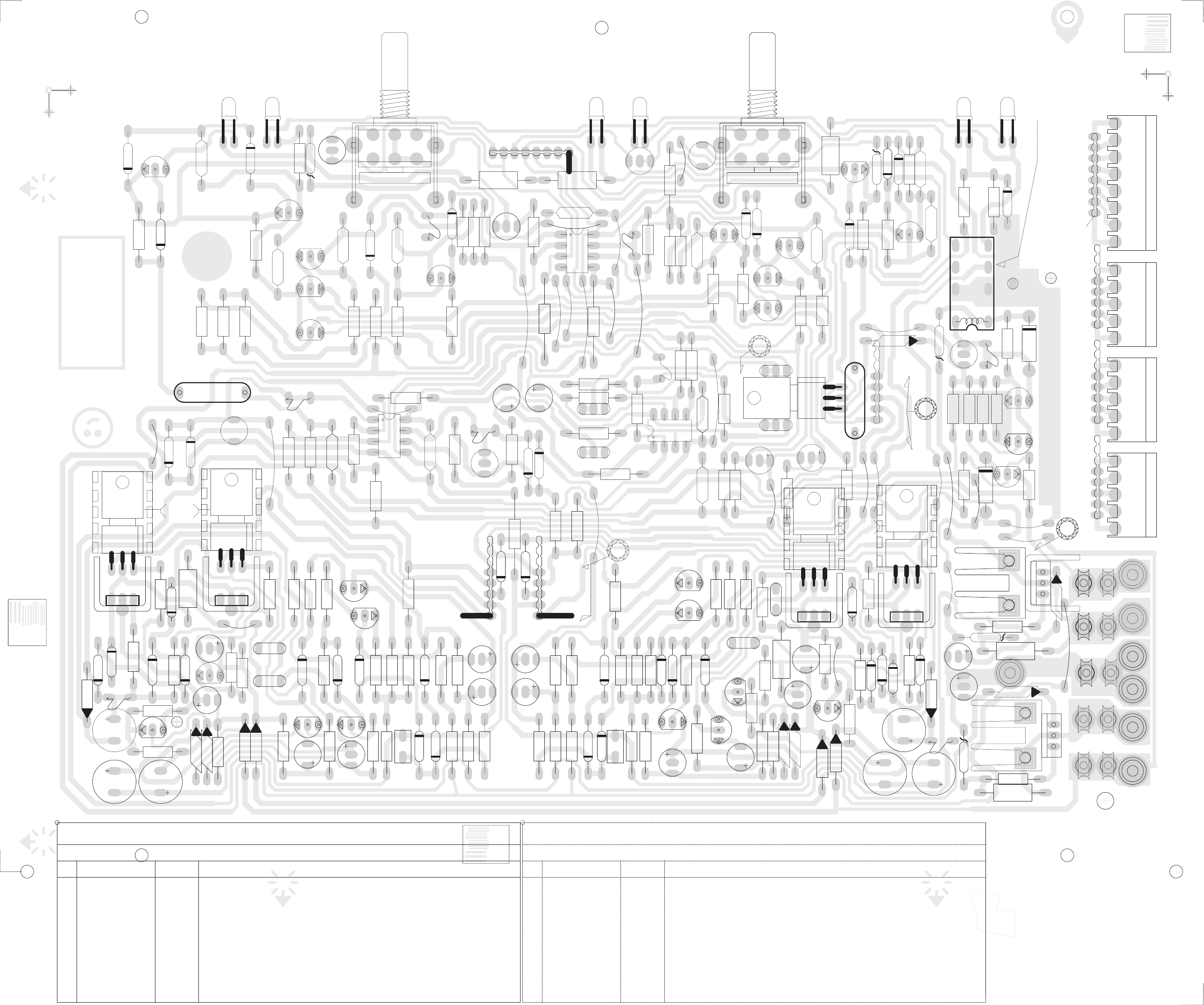
SHEAR SHEAR
ROUTE
GAGE
0.01"/HOLE
.020"
.012"
.008"
.005"
VCD
.020"
.012"
.008"
.005"
SHEAR SHEAR
.020"
.012"
.008"
.005"
5.13
SOLDERSIDE M1011-5.10
BLANK SIZE=16.000"X11.050"
M1011-
RED
YEL
BLK
WHT
BLU
POW SUP
BOTTOM INPUT BOARD
TOP
TJH1
GUIDE
ETCH
EY16
F
HS1
PART#
HS2
PART#
R60B 2_WATT
220K
@R8
J1
J9
HS3
PART#
MS4
8POS.RT.ANGLE_MOLEX
#XXXX
INPUT_BOARD
D21B
4148
D21A
4148
1
_MW1
FUNCTION
PART#
Q19B
MJE350
TP6
TP5
C22B
@C1
300V
10P
C23B
@C1
300V
10P
C22A
@C1300V
10P
C23A
@C1
300V
10P
Q19A
MJE350
Q18A
MJE340
Q18B
MJE340
C27B
@C2
160V
10U
C28B
@C2
160V
10U
C28A
@C2
160V
10U
C27A
@C2
160V
10U
R103
@R3
0.5W
15K
R102
@R3
0.5W
15K
MS1
AMP_A
R60A
@R8
2WATT
220K
HS6
PART#
C20A
22N
C20B
22N
MS2
AMP_B
1
MW4
Q12B
@Q3
MPSA42
Q13B
@Q4
MPSA92 Q13A @Q4
MPSA92
Q12A
@Q3
MPSA42
D35
BAV21
C29A
330U
16V
D19B
4148
J27
C16
10u
16V
Q21A
2V5
NJM431
J15
ZD8
20V
C28
10u
16V
1
MW1
Q14B
BC560 Q17B
BC550 Q17A
BC550
Q14A
BC560
D14B
4148
D13B
4148
D15B
4148
D16B
4148
D17B
4148
D18B
4148
D20B
4148
D22A
4148
D23A
4148
D19A
4148
R100 100K
D18A
4148
D17A
4148
D16A
4148
D15A
4148
D13A
4148
D14A
4148
D23B
4148
D22B
4148
D50
4148
D51
4148
C48
100U
25V
C18B
22U
16V
C19B 22U
16V
C21B
22U
10V
C24B
22U
10V
C25A
4U7
10V
C26A
4U7
10V
C24A
22U
10V
C21A
22U
10V
C19A
22U
16V C18A
22U
16V
C49
100U
25V
C26B 4U7
10V
C25B
4U7
10V
C29 100N
R40B
220R
R39B 7K5
R41B 7K5
R38B
7K5
R42B
7K5
R44B 1K
R45B
1K
R46B 4K7
R47B 1K5
R48B
1K5
R49B
470R
R50B 4K7
R51B
1K5
R52B
1K5
R53B470R
R43B
3K
R56B
17K8
R55B
@R5
21K5
1
MW2
R66A
10R
R61A
@R9
47R
R62A
@R9
47R
R63A 39R
Q20A
2V5
NJM431
1
MW3
R55A
@R5
21K5
R64B
@R7
150R
R57B
@R7
150R
R56A 17K8
R43A
3K
R53A
470R
R52A
1K5
R51A 1K5
R50A 4K7
R49A
470R
R48A
1K5
R47A 1K5
R46A 4K7
R45A 1K
R44A 1K
R42A
7K5
R38A
7K5
R41A
7K5
R39A
7K5
R40A
220R
R65B10R
Q37
BC550
R105
1K
R104 1K
R58B 39R
R63B 39R
R62B
@R9
47R
MS3
POWER_SUPPLY
R61B
@R9
47R
1
_MW2
R66B
10R
11
10
9
8
7
6
5
4
3
2
1
# DESCRIPTION OF CHANGE
VER#
DATE
MODEL(S):-
D
D
D
D
D
D
D
OCT/27/97
FEB/15/95
NOV/29/94
JUN/22/94
V
V
V
V
V
V
V
5.12
5.10
5.00
4.53
N
N
N
N
N
N
N
PC#5497_R66A/B_1/8WFP->1/4WFP
Q14A/Q21A_MOVED_TO_AID_RAD_INSERT
PC4651_LED’S->NJM431+2_RESISTORS
PC#4529_BD651->BDX53C_BD652->BDX54C
AP-3000
M1011.PCB_DATABASE_HISTORY
R65A10R
EY13
F
Q21B
2V5
NJM431
EY1
EY4
EY7
TJH2
GUIDE
ETCH
EY10
EY9
F
2
J14
J4
C5
2U2
63V
J6
R59A10R
D9
4148
D20A
4148
J10
BE
Q31
BDX54C
FUNCTION
1
C27
220P
J18
J16
C14
2U2
63V
J23
BE
Q30
BDX53C
FUNCTION
1
_MW4
R11249R
TP9
TP4
TP3
TP2
TP1
NO NC C
RE1
AROMAT_RELAY
#3699
48V_COIL
C43 220N
250V
C42
220N
250V
P2
25A10K
PT#4400
P1
25A10K
PT#4400
R99
@R6
1/4W
330R
R98
@R6
1/4W
330R
R124
@R13
0.5W
1K5 EB
Q11
PART#
FUNCTION
BF872
D48
1N4004
ZD17
@ZD1
10V
C31
27P
1
_MW3
FUNCTION
C32
27P
Q28
A63
Q29
A13
Q38
@Q5
MPSA92
Q36
@Q6
2N5551
Q10
A63
Q5
A63
C17
47U
10V
C9
47U
10V
ZD2
4V7
ZD1
4V7
E B
Q16B
@Q2
TIP50
Q8
BC550
Q6
BC560
Q7
BC550
Q9
BC550
Q4
BC550
Q2
BC550
Q1
BC560
Q3
BC550
D36
BAV21
J19
J11
D5
4148
D11
4148
D49
1N4004
D12
4148
D6
4148
D8
4148
D7
4148
D10
4148
D46
4148
J21
D3
4148
D4
4148
D1
4148
D2
4148
RV1
100K
C52
4U7
63V
C10
1U
16V
C3
1U
16V
U2
@U1
33078
U1
@U1
33078
C6
100N
C1247P
C11 47P
C13 100N
RV2
100K
RV3
100K
RV4
100K
C4
100N
C147P
C2
47P
-
+
LD4
GRN
-
+
LD3
GRN
-
+
LD5
RED
-
+
LD2
RED
-
+
LD6
GRN
-
+
LD1
RED
R96
100K
C23
220P
R97
470K
R101
470K
R54B
47K
J26
R132
1K5
R131
1K5
R128
220K
R129
1M
R127
4K7
R126
10K
R32
249R
R12
249R
R34
10K0
R33
10K0
R30 820R
R231K
R31
220K
R25 17K8
R35249R
R241K
R26
3K
R29
3K
R27
47K
R28
47K
R125
270R
@10R
R130
10K
R19 45K3
@R14
R7
47K
R547K
R21
10K0
R18
270R270R
R83K
R63K
R41K
R1
@R1
5K36
R317K8
R15
@R2
113K0
R2010K0
R16
@R2
113K0
R17 270R270R
R10
220K
R36
330R
R21K
R13
10K0
R14
10K0
R9
820R
J24
U3
@U1
33078
R42
10K0
R40 10K0
R45
10K0
R44
10K0
R38 82K5
R39 82K5
R43
82K5
R41
82K5
PART#
E B
Q15A
@Q1
MJE5730
E B
Q15B
MJE5730
@Q1
E B
Q16A
@Q2
TIP50
J13
J5
R58A 39R
C26
100N
R69B
@R11
33K
J17
J20
ZD7
20V
J22
J25
J8
R68A
@R12
68K
J7
R22
@R1
5K36
J28
GUIDE
ETCH
EY11
EY14
R69A
@R11
33K
HS5
PART#
J29
J3
C29B
330U
16V
R54A 47K
2
3
R106 10R
R37
@R4
15R
R107
10R
R59B
10R
R57A
@R7
150R
R64A
@R7
150R
Q20B
2V5
NJM431
R70A
@R12
68K
R70B
@R12
68K
R68B
@R12
68K
R67B
@R11
33K
R67A
@R11
33K
C25
10u
16V
C15
10u
16V
EY6
F
EY3
F
EY2
F
EY5
F
EY8
F
EY12
F
EY15
F
11
10
9
8
7
6
5
4
3
2
1
# DESCRIPTION OF CHANGEVER#DATE
MODEL(S):-
D
OCT/27/97
APR/08/97
FEB/15/95
NOV/29/94
JUN/22/94
FEB/94
JAN/18/94
.
AUG/06/93
V
5.12
5.11
5.10
5.00
4.53
4.52
4.52
.
4.51
N
PC#5497_R66A/B_1/8WFP->1/4WFP
PC#5353_R60A/B->2_WATT
Q14A/Q21A_MOVED_TO_AID_INSERTION
PC#4651_LED’S->NJM431+2_RESISTORS
PC#4529_BD651->BDX53C_BD652->BDX54C
PC#4545_R1/R22_6K2->5K36
PC#4533_R19_43K->45K3
R19_51K->43K
PC#4443_R17,R18_470R->270R
AP-3400
M1011A.PCB_DATABASE_HISTORY
EY17
-55
-18
+18
+100
-100
+55
R+
L+
-18M
L+M
R-M
L-M
R+M
+18M
R-
L-
GND
NC
NC
NC
NC
ASSEMBLY M1011-5.13
BLANK SIZE=16.000"X11.050"
PCB MECH M1011-5.13
BLUE
BLUE
WHT
WHT
BLK
BLK
BLKL
YELL
YELL
RED
RED
TO BE HAND INSERTED
INSERTED C3 1U 16V
1 RV2,RV4 TO BE HAND
PRODUCTION NOTES
HOLE
AZ
PT#4790
WIRE
BLK
WIRE
BLK
VER 5.13
AP-3400
M1011A
48V COIL
DOWN
DOWN
FACE
FACE
M1011A
NOTE RELAY HAS
AUG/05/98 5.13 PC#5528_Q16 A,B REPLACE WITH TIP50#6891
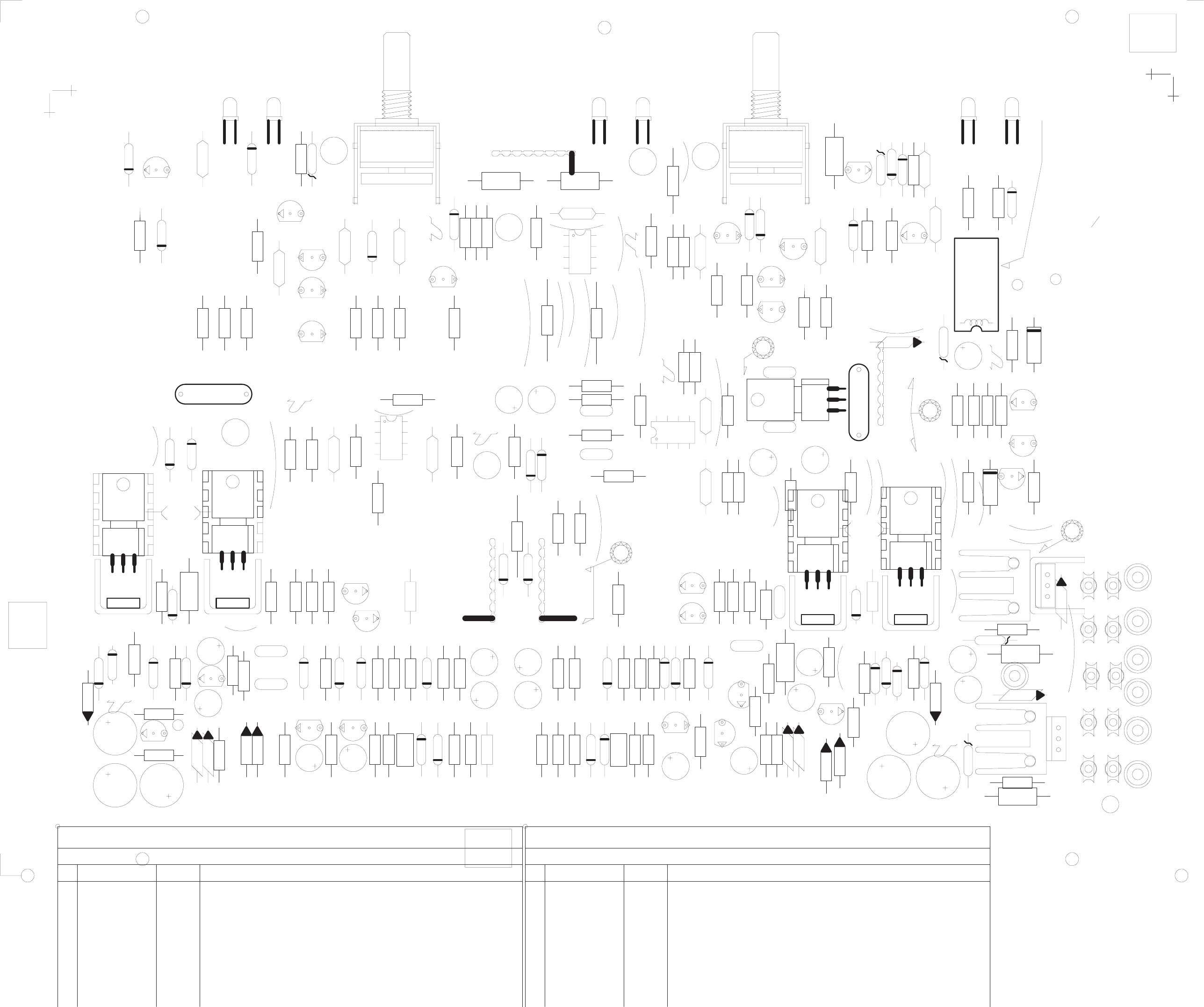
TJH1
GUIDE
ETCH
EY16
F
HS1
PART#
HS2
PART#
R60B 2_WATT
220K
@R8
J1
J9
HS3
PART#
D21B
4148
D21A
4148
1
_MW1
FUNCTION
PART#
Q19B
MJE350
TP6
TP5
C22B
@C1
300V
10P
C23B
@C1
300V
10P
C22A
@C1 300V
10P
C23A
@C1
300V
10P
Q19A
MJE350
Q18A
MJE340
Q18B
MJE340
C27B
@C2
160V
10U
C28B
@C2
160V
10U
C28A
@C2
160V
10U
C27A
@C2
160V
10U
R103
@R3
0.5W
15K
R102
@R3
0.5W
15K
R60A
@R8
2WATT
220K
HS6
PART#
C20A
22N
C20B
22N
Q12B
@Q3
MPSA42
Q13B
@Q4
MPSA92 Q13A @Q4
MPSA92
Q12A
@Q3
MPSA42
D35
BAV21
C29A
330U
16V
D19B
4148
J27
C16
10u
16V
Q21A
2V5
NJM431
J15
ZD8
20V
C28
10u
16V
Q14BBC560 Q17B
BC550 Q17A
BC550
Q14A
BC560
D14B
4148
D13B
4148
D15B
4148
D16B
4148
D17B
4148
D18B
4148
D20B
4148
D22A
4148
D23A
4148
D19A
4148
R100 100K
D18A
4148
D17A
4148
D16A
4148
D15A
4148
D13A
4148
D14A
4148
D23B
4148
D22B
4148
D50
4148
D51
4148
C48
100U
25V
C18B
22U
16V
C19B 22U
16V
C21B
22U
10V
C24B
22U
10V
C25A
4U7
10V
C26A
4U7
10V
C24A
22U
10V
C21A
22U
10V
C19A
22U
16V
C18A
22U
16V
C49
100U
25V
C26B 4U7
10V C25B
4U7
10V
C29 100N
R40B
220R
R39B 7K5
R41B 7K5
R38B
7K5
R42B
7K5
R44B 1K
R45B
1K
R46B 4K7
R47B 1K5
R48B
1K5
R49B
470R
R50B 4K7 R51B
1K5
R52B
1K5
R53B470R
R43B
3K
R56B
17K8
R55B
@R5
21K5
R66A
10R
R61A
@R9
47R
R62A
@R9
47R
R63A 39R
Q20A
2V5
NJM431
R55A
@R5
21K5
R64B
@R7
150R
R57B
@R7
150R
R56A 17K8
R43A
3K
R53A
470R
R52A
1K5
R51A 1K5
R50A 4K7
R49A
470R
R48A
1K5
R47A 1K5
R46A 4K7
R45A 1K
R44A
1K
R42A
7K5
R38A
7K5
R41A
7K5
R39A
7K5
R40A
220R
R65B10R
Q37
BC550
R105
1K
R104 1K
R58B 39R
R63B 39R
R62B
@R9
47R
R61B
@R9
47R
1
_MW2
R66B
10R
11
10
9
8
7
6
5
4
3
2
1E
G
N
A
H
C
F
O
N
O
I
T
P
I
R
C
S
E
D# VER#DATE
MODEL(S):-
D
D
D
D
D
D
D
OCT/27/97
FEB/15/95
NOV/29/94
JUN/22/94
V
V
V
V
V
V
V
5.12
5.10
5.00
4.53
N
N
N
N
N
N
N
PC#5497_R66A/B_1/8WFP->1/4WFP
Q14A/Q21A_MOVED_TO_AID_RAD_INSERT
PC4651_LED’S->NJM431+2_RESISTORS
PC#4529_BD651->BDX53C_BD652->BDX54C
AP-3000
M1011.PCB_DATABASE_HISTORY
R65A10R
EY13
F
Q21B
2V5
NJM431
EY1
EY4
EY7
TJH2
GUIDE
ETCH
EY10
EY9
F
2
J14
J4
C5
2U2
63V
J6
R59A10R
D9
4148
D20A
4148
J10
BE
Q31
BDX54C
FUNCTION
1
C27
220P
J18
J16
C14
2U2
63V
J23
BE
Q30
BDX53C
FUNCTION
1_MW4
R11249R
TP9
TP4
TP3
TP2
TP1
NO NC C
RE1
AROMAT_RELAY
#3699
48V_COIL
C43 220N
250V
C42
220N
250V
P2
25A10K
PT#4400
P1
25A10K
PT#4400
R99
@R6
1/4W
330R
R98
@R6
1/4W
330R
R124
@R13
0.5W
1K5 EB
Q11
PART#
FUNCTION
BF872
D48
1N4004
ZD17
@ZD1
10V
C31
27P
1
_MW3
FUNCTION
C32
27P
Q28
A63
Q29
A13
Q38
@Q5
MPSA92
Q36
@Q6
2N5551
Q10
A63
Q5
A63
C17
47U
10V
C9
47U
10V
ZD2
4V7
ZD1
4V7
E B
Q16B
@Q2
Q8
BC550
Q6
BC560
Q7
BC550
Q9
BC550
Q4
BC550
Q2
BC550
Q1
BC560
Q3
BC550
D36
BAV21
J19
J11
D5
4148
D11
4148
D49
1N4004
D12
4148
D6
4148
D8
4148
D7
4148
D10
4148
D46
4148
J21
D3
4148
D4
4148
D1
4148
D2
4148
RV1
100K
C52
4U7
63V
C10
1U
16V
C3
1U
16V
U2
@U1
33078
U1
@U1
33078
C6
100N
C1247P
C11 47P
C13 100N
RV2
100K
RV3
100K
RV4
100K
C4
100N
C147P
C2
47P
-
+
LD4GRN
-
+
LD3
GRN
-
+
LD5
RED
-
+
LD2
RED
-
+
LD6
GRN
-
+
LD1
RED
R96
100K
C23
220P
R97
470K
R101
470K
R54B
47K
J26
R132
1K5
R131
1K5
R128
220K
R129
1M
R127
4K7
R126
10K
R32
249R
R12
249R
R34
10K0
R33
10K0
R30 820R
R231K
R31
220K
R25 17K8
R35249R
R241K
R26
3K
R29
3K
R27
47K
R28
47K
R125
270R
@10R
R130
10K
R19 45K3
@R14
R7
47K
R547K
R21
10K0
R18
270R270R
R83K
R63K
R41K
R1
@R1
5K36
R317K8
R15
@R2
113K0
R2010K0
R16
@R2
113K0
R17 270R270R
R10
220K
R36
330R
R21K
R13
10K0
R14
10K0
R9
820R
J24
U3
@U1
33078
R42
10K0
R40 10K0
R45
10K0
R44
10K0
R38 82K5
R39 82K5
R43
82K5
R41
82K5
PART#
E B
Q15A
@Q1
MJE5730
E B
Q15B
MJE5730
@Q1
E B
Q16A
@Q2
J13
J5
R58A 39R
C26
100N
R69B
@R11
33K
J17
J20
ZD7
20V
J22
J25
J8
R68A
@R12
68K
J7
R22
@R1
5K36
J28
GUIDE
ETCH
EY11
EY14
R69A
@R11
33K
HS5
PART#
J29
J3
C29B
330U
16V
R54A 47K
2
3
R106 10R
R37
@R4
15R
R107
10R
R59B
10R
R57A
@R7
150R
R64A
@R7
150R
Q20B
2V5
NJM431
R70A
@R12
68K
R70B
@R12
68K
R68B
@R12
68K
R67B
@R11
33K
R67A
@R11
33K
C25
10u
16V
C15
10u
16V
EY6
F
EY3
F
EY2
F
EY5
F
EY8
F
EY12
F
EY15
F
11
10
9
8
7
6
5
4
3
2
1EGNAH
C FO NOITP
I
R
C
S
E
D
#VER#
DATE
MODEL(S):-
D
OCT/27/97
APR/08/97
FEB/15/95
NOV/29/94
JUN/22/94
FEB/94
JAN/18/94
.
AUG/06/93
V
5.12
5.11
5.10
5.00
4.53
4.52
4.52
.
4.51
N
PC#5497_R66A/B_1/8WFP->1/4WFP
PC#5353_R60A/B->2_WATT
Q14A/Q21A_MOVED_TO_AID_INSERTION
PC#4651_LED’S->NJM431+2_RESISTORS
PC#4529_BD651->BDX53C_BD652->BDX54C
PC#4545_R1/R22_6K2->5K36
PC#4533_R19_43K->45K3
R19_51K->43K
PC#4443_R17,R18_470R->270R
AP-3400
M1011A.PCB_DATABASE_HISTORY
EY17
-55
-18
+18
+100
-100
+55
R+
L+
-18M
L+M
R-M
L-M
R+M
+18M
R-
L-
GND
NC
NC
NC
NC
ASSEMBLY M1011-5.13
BLANK SIZE=16.000"X11.050"
PCB MECH M1011-5.13
BLUE
BLUE
WHT
WHT
BLK
BLK
BLKL
YELL
YELL
RED
RED
TO BE HAND INSERTED
INSERTED C3 1U 16V
1 RV2,RV4 TO BE HAND
PRODUCTION NOTES
HOLE
AZ
PT#4790
WIRE
BLK
WIRE
BLK
VER 5.12
AP-3400
M1011A
48V COIL
DOWN
DOWN
FACE
FACE
M1011A
NOTE RELAY HAS
P:\1011APRT.PRN
TIP50
TIP50
AUG/05/98 5.13 PC#5528_Q16 A,B REPLACE WITH TIP50#6891
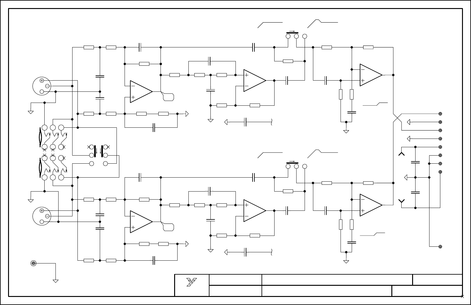
1/2
5532
U3
2
31
4M7
R14
16v 470n
C7
OUT
IN
S1
1
2
3
1/2
5532
U3
6
57
17K8:1%
R15
16v 150n
C9
16v 47n
C8
16v
100n
C6
16v 68n
C5
SRT
CH_B_IN
NO_GOLD
JB2 1
2
3
4
5
6
NUTRIX
BAL_IN
JB1
13
2
1/2
33078
U1
2
31
1K
R5
10K:1%
R6
1K
R1
10K:1%
R2
14K0:1%
R3
14K0:1%
R7
470p
C1
470p
C2
100p
C3
100p
C4
EY2
WC1
5K6
R12
1R
R4 7K5
R13
1/2
33078
U1
6
57
17K8:1%
R11
17K8:1%
R10
10K:1%
R9
82K5:1%
R17
82K5:1%
R35
10K:1%
R27
17K8:1%
R28
17K8:1%
R29
1/2
33078
U2
2
31
7K5
R31
1R
R26 5K6
R30
100p
C14
100p
C13
470p
C12
470p
C11
14K0:1%
R22
14K0:1%
R25
10K:1%
R24
1K
R23
10K:1%
R21
1K
R20
1/2
33078
U2
6
57
NUTRIX
BAL_IN
JB4
13
2
SRT
CH_A_IN
NO_GOLD
JB3 1
2
3
4
5
6
YORKVILLE
NAME: PCB#&VER:
MODELS: SCH ISSUE:
TITLE:
DATE:
M1012-2.00
AP-3400
AUDIO-PRO
M1012A.SCH
SEP/19/94
INPUT_&_FILTER
0.00
16v 68n
C15
16v
100n
C16 16v 47n
C18 16v 150n
C19
17K8:1%
R33
470R
R16
OUT
IN
S1
4
5
6
16v 470n
C17
4M7
R32 470R
R34
T7
T6
T5
T4
T3
T8
T1
100n
C23
100n
C24
100n
C21
100n
C22
1K5
R18
1K5
R36
16v
6n8
C10
16v
6n8
C20
1
2
T2
OUT
IN
S2
1
2
3
OUT
IN
S2
4
5
6
SIG_R
GND
GND
GND
GND
+18
+18
-18
-18
SIG_L
18Ga BLACK WIRE
REF_L
REF_R
LEFT = CHAN A
RIGHT = CHAN B
GROUND STRAP:
GREEN WIRE TO
TO M1011 GND
+2dB
+2dB
IN = MONO
MUST BE BREAK BEFORE MAKE, #3436
MUST BE BREAK BEFORE MAKE, #3436
20KHz
20KHz
TO PIN 4 OF 5532
TO PIN 4 OF 5532
-1dB 30Hz
-1dB 30Hz
+4dB 55Hz
+4dB 55Hz
FILTER
FILTER
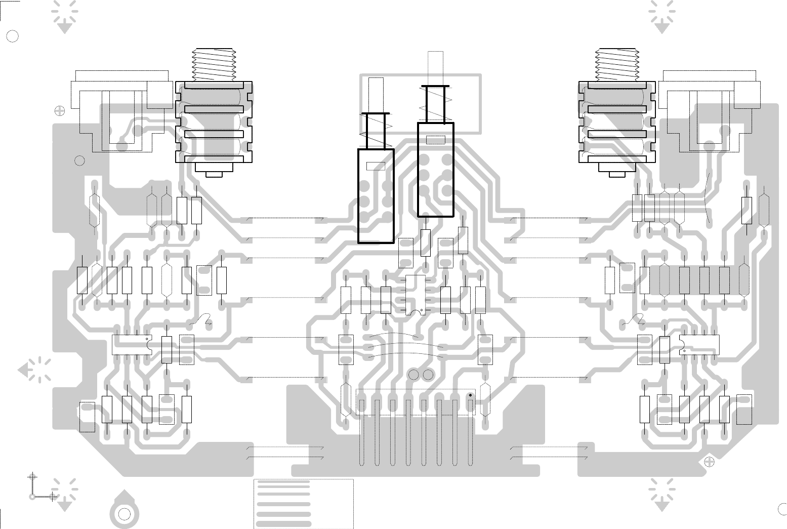
VCD
.025"
.030"
.040"
.050"
.060"
SHEAR SHEAR
SHEAR
SHEAR SHEAR
2.00
2.00
SOLDERSIDE M1012-2.00
1.20
SEPT’89
M1012
M1012
M1012
BLANK SIZE=15.700"X10.000"
55
44
1
DRILL DETL M1012-2.00
U3
5532
40
40
40
4040
40
40
40
U1
33078
@U1
40404040
40 40 40 40
U2
33078
@U1
40 40 40 40
40404040
R14
4M7
40
40
R15
17K8
40
40
R5
1K
40
40
R6
10K0
40
40
R1
1K
40
40
R2
10K0
40
40
R3
14K0
@R1
40
40
R7
14K0
@R1
40
40
BUT1
GREY_BUTTON
R12
5K6
40
40
R4
1R
40
40
R13
7K5
40
40
R11
17K8
40
40
R10
17K8
40
40
R9
10K0
40
40
R17
82K5
40
40
R35
82K5
40
40
R27
10K0
40
40
R28
17K8
40
40
R29
17K8
40
40
R31
7K5
40
40
R26
1R
40
40
R30
5K6
40
40
S2
MONO
#3436
47
42
47
47
42
47
R22
14K0
@R1
40
40
R25
14K0
@R1
40
40
R24
10K0
40
40
R23
1K
40
40
R21
10K0
40
40
R20
1K
40
40
R33
17K8
40
40
R16
470R
40
40
R32
4M7
40
40
R34
470R
40
40
R18
1K5
40
40
R36
1K5
40
40
C7
470N
40
40
C9
150N
40
40
C8
47N
40
40
C6
100N
40
40
C5
68N
40
40
C15
68N
40
40
C16
100N
40
40
C18
47N
40
40
C19
150N
40
40
C17
470N
40
40
C10
6N8
40
40
C20
6N8
40
40
J17
52 52
J18
52 52
JB3
UNBAL_IN_B
59 59
59 59
59 59
40
40
C1
470P
40
40
C2
470P
40
40
C3
100P
40
40
C4
100P
40
40
C14
100P
40
40
C13
100P
40
40
C12
470P
40
40
C11
470P
40
40
C23
100N
40
40
C24
100N
40
40
C21
100N
40
40
C22
100N
40
40
J7
52 52
LINEWIDTH GAUGE
TP1
40 40
TP2
40 40
99
B_BAL_INPUT
PART#
PT#3660
52 52
47
J6
52 52
J8
52 52
JB2
UNBAL_IN_A
59 59
59 59
59 59
BUT2
GREY_BUTTON
J5
52 52
J3
52 52
J4
52 52
J1
52 52
J11
52 52
J13
52 52
J14
52 52
J15
52 52
J16
52 52
MC1
FUNCTION
5959595959595959
16 16 16 16 16 16 16 16
30
3030
30
30
30
30
S1
#3436
BASS_BOOST
47
42
47
47
42
47
J19
40 40
30
30
30
30
30
30
30
30
30
30
30
30
30
30
30
30
5
5
40
5
1515
30
30
J2
52 52
15
30
30
128
TJH1
128
TJH2
J12
52 52
WC1
82
J10
40 40
J9
40 40
1515
WC2
82
99
A_BAL_INPUT
PT#3660
52 52
47
ASSEMBLY M1012-2.10 BLANK SIZE=15.700"X10.000"
PCB MECH M1012-2.00
SWITCH/S
GRN
BLK 13"
AZ HOLE
16AWG
16AWG
REF_R
SIG_R
REF_L
SIG_L
ARE #3436
MAKE!!!!
BEFORE
BREAK
-18V
GND
GND
+18V
VER. 2.10
AP-3400
M1012A
AP-3400
M1012A
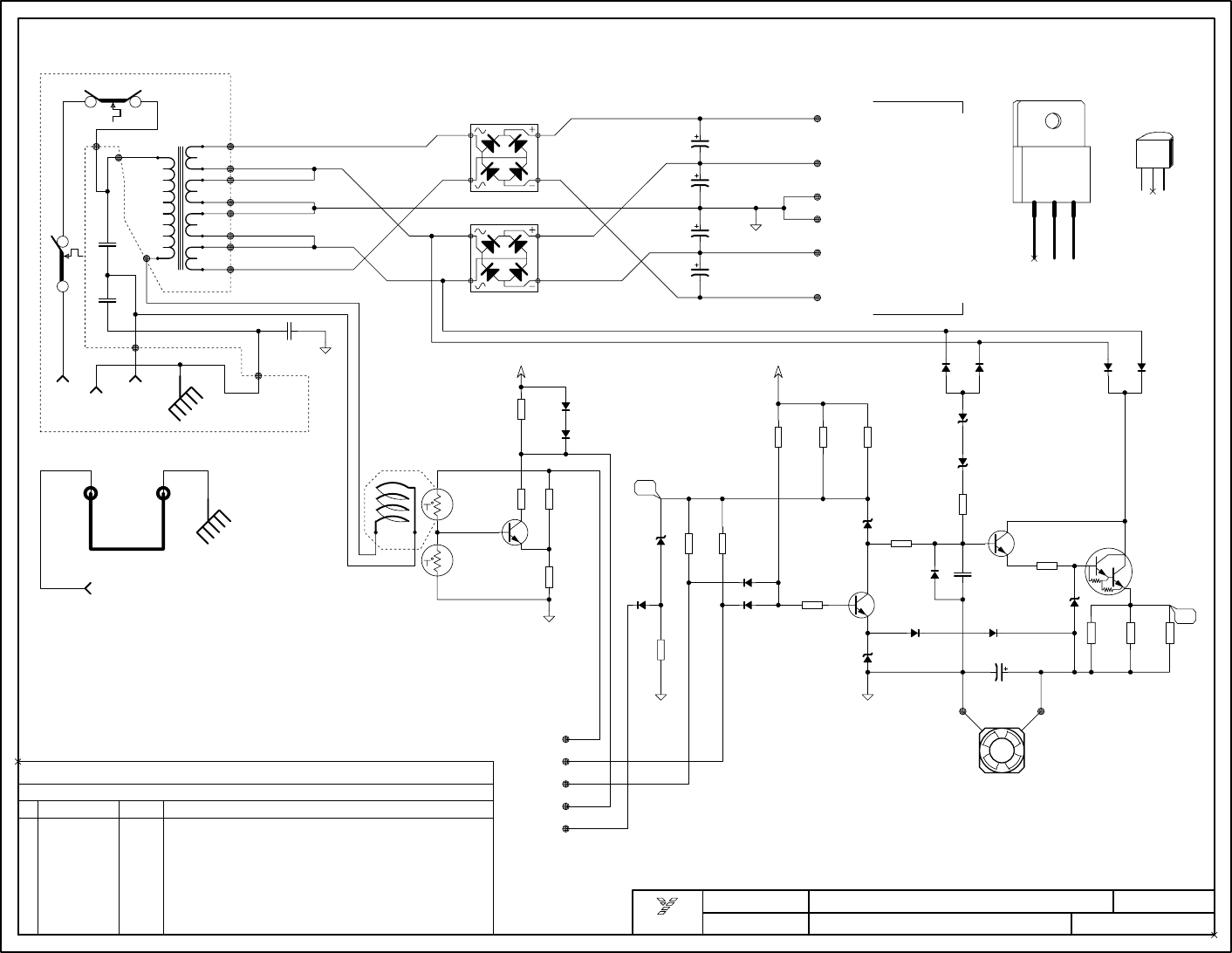
WC3
MC1
1
40CFM
FAN
22n
CSA
C54
MC1
2
D47
7K5
R123
33v
500mW
ZD15
27K
R116
8
7
MC1
3
MC1
4
MC1
5
WC8
WC6
WC4
WC7
EY7
EY6
EY3
EY5
EY10
WC11
WC1
1K
R124
D48
EY13 EY14
D37
D46
22nCSA C53
4n7
CSA
C55
EY4
EY2
EY11
D41
4v7
500mW
ZD10
2R2
0.5W
R122
D40
MJH11018
Q35
EY8
1N4004
D45
470u25v C51
1N4004
D44
25v
22n
C50
A06
Q33
4v7
500mW
ZD11
68K
R113 68K
R112
D39
D38
22K
R118
1.2M
R114 33V
500mW
ZD12
33V
500mW
ZD13
1N4004
D43 1N4004
D42
15K
R117
220R
R119
2N5551
Q34
47K
R108
2R2
0.5W
R121
47K
R109
17K8:1%
R111
14K0:1%
R110
2N5551
Q32
100K
RV6
100K
RV5
13A/85C
TB2
12A/SW
TB1
L1
MJH11018
ECB
MPSA06
EBC
2N5551
2R2
0.5W
R120
10
9
8
7
6
5
4
3
2
1
# DESCRIPTION OF CHANGEVER#DATE
MODEL(S):-
D
D
D
D
D
D
D
D
D
AUG/12/97
V
V
V
V
V
V
V
V
V
1.40
N
N
N
N
N
N
N
N
N
PC#5444_R120->122_1/4W->1/2W
AP3400
M1013A.SCH_DATABASE_HISTORY
WC10
EY12
EY9
YORKVILLE
NAME: PCB#&VER:
MODELS: SCH ISSUE:
TITLE:
DATE:
M1013A
AP-3400
M1013A.SCH
AUG/12/97
SUPPLY/FAN_PCB
1.40
330u
80V
C47
330u
80V
C46
330u
80V
C45
330u
80V
C44
13AMP
DB2
3
4
1
2
13AMP
DB1
3
4
1
2
UI
YSL#
120VAC
1KVA
TYPE_H
TR1
4v7
500mW
ZD14
27K
R115
WHITE
BLACK
CHASSIS
KILL
GND
GND GND
GND
GND
GND
+78 +78
+78
+18
RTSENSE
LTSENSE
RMS
-78
-145
+145
TO M1011A:
HIGH CURRENT TO M1011A
TO WC1 ON M1012
BLUE
WHITE
BLACK
BLACK
YELLOW
RED
UNDER CAP:
ALL UNMARKED DIODES ARE 1N4148.
ACTUAL PARTS MAY HAVE HIGHER VOLTAGE RATINGS.
NOTE: CAPACITOR VOLTAGE RATINGS SHOWN ARE MINIMUM REQUIRED.
BLK
BLK
WHITE
BLUE
BLUE
YELLOW
YELLOW
RED
RED
GREY
120 VAC 60 Hz LINE
STRAP
GROUND
RMS IN
AMBIENT
10.7v
5 WATTS
ABOUT
SENSOR:
530uA
220uA
IDLE
15.6v
13.5v
13 A = 15K
11 A = 33K
AT 25~ AMBIENT:
28v @ 80~
10K @ 80~
25K @ 55~
50K @ 40~
100K @ 25~
GREEN
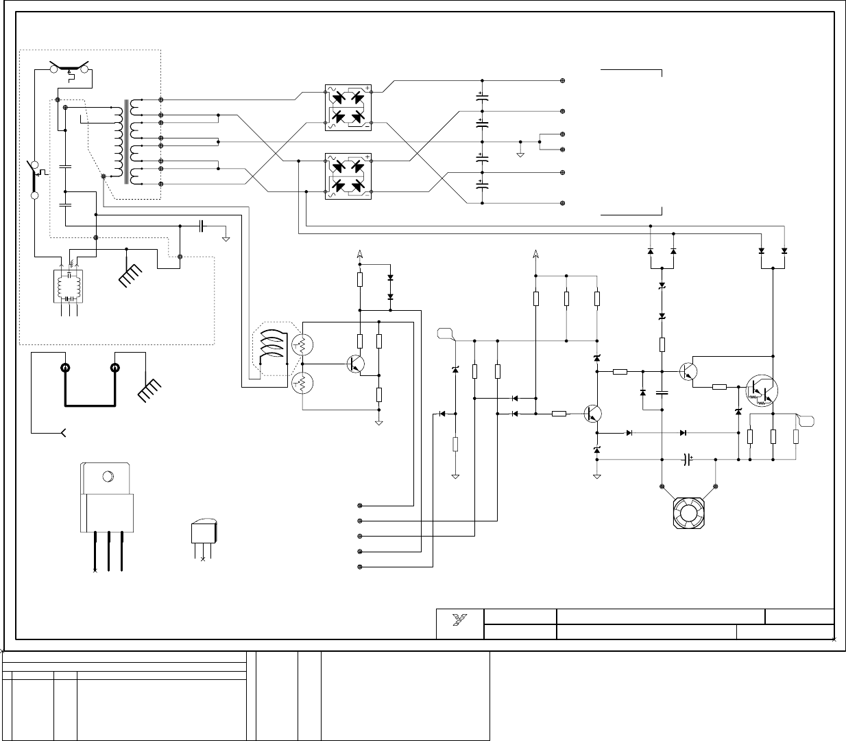
WC3
MC1
1
40CFM
FAN
22n
CSA
C54
MC1
2
D47
7K5
R123
33v
500mW
ZD15
27K
R116
8
7
MC1
3
MC1
4
MC1
5
WC8
WC6
WC4
WC7
EY7
EY6
EY3
EY5
EY10
WC11
WC1
1K
R124
D48
EY13 EY14
D37
D46
22nCSA C53
4n7
CSA
C55
EY4
EY2
EY11
D41
25
24
23
22
21
20
19
18
17
16
15
14
13
12
11
10
9
8
7
6
5
4
3
2
1
# DESCRIPTION OF CHANGEVER#DATE
MODEL(S):-
D
D
D
D
D
D
D
D
D
SEPT/28/95 V
V
V
V
V
V
V
V
V
V
1.40 N
N
N
N
N
N
N
N
N
N
PC#4883
AP-3400E
M1013AE.SCH_DATABASE_HISTORY
4v7
500mW
ZD10
2R2
R122
D40
MJH11018
Q35
EY8
1N4004
D45
470u25v C51
1N4004
D44
25v
22n
C50
2R2
R121
A06
Q33
4v7
500mW
ZD11
68K
R113 68K
R112
D39
D38
22K
R118
1.2M
R114
2R2
R120
33V
500mW
ZD12
33V
500mW
ZD13
1N4004
D43 1N4004
D42
15K
R117
220R
R119
2N5551
Q34
47K
R108
AC LINE FILTER
BLU
GRN/YEL
BRN
47K
R109
17K8:1%
R111
14K0:1%
R110
2N5551
Q32
100K
RV6
100K
RV5
13A/85C
TB2
8A/SW
TB1
L1
MPSA06
EBC
2N5551
MJH11018
ECB
YORKVILLE
NAME: PCB#&VER:
MODELS: SCH ISSUE:
TITLE:
DATE:
M1013A-2.20
AP-3400E
M1013AE.SCH
SEP/28/95
SUPPLY/FAN_PCB
1.40
WC10
EY12
EY9
330u
80V
C47
330u
80V
C46
330u
80V
C45
330u
80V
C44
13AMP
DB2
3
4
1
2
13AMP
DB1
3
4
1
2
YSL#1288E
220/240VAC
TR1
4v7
500mW
ZD14
27K
R115
BLUE
CHASSIS
KILL
GND
GND GND
GND
GND
GND
+78 +78
+78
+18
RTSENSE
LTSENSE
RMS
BROWN
-78
-145
+145
ADDED EMI AC LINE FILTER
EY3 FOR 220V
GREEN WIRE TO
EY3 FOR 240V
ORANGE WIRE TO
220/240 VAC 50 Hz LINE
240V
220V
BRN
GRN
ORN
TO M1011A:
HIGH CURRENT TO M1011A
TO WC1 ON M1012
BLUE
WHITE
BLACK
BLACK
YELLOW
RED
UNDER CAP:
ALL UNMARKED DIODES ARE 1N4148.
ACTUAL PARTS MAY HAVE HIGHER VOLTAGE RATINGS.
NOTE: CAPACITOR VOLTAGE RATINGS SHOWN ARE MINIMUM REQUIRED.
WHITE
BLUE
BLUE
YELLOW
YELLOW
RED
RED
GREY
STRAP
GROUND
RMS IN
AMBIENT
10.7v
5 WATTS
ABOUT
SENSOR:
530uA
220uA
IDLE
15.6v
13.5v
13 A = 15K
11 A = 33K
AT 25~ AMBIENT:
28v @ 80~
10K @ 80~
25K @ 55~
50K @ 40~
100K @ 25~
GRN/YEL
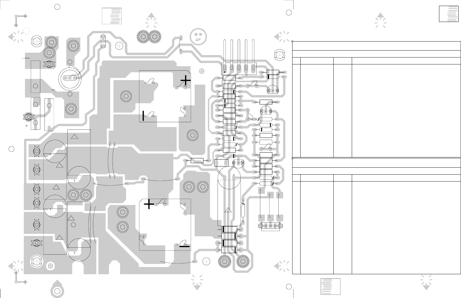
.020"
.012"
.008"
.005"
SHEAR
SHEARSHEAR
SHEAR
SHEARSHEAR
SHEARSHEAR
VCD
.020"
.012"
.008"
.005"
.020"
.012"
.008"
.005"
SOLDERSIDE M1013-2.30
2.30
BLANK SIZE=12.600"X6.500"
M1013-
2 OZ COPPER
DRILL DETL M1013-2.30
TJH2
L1
#3822
C44
@C1 80V
330U
C45
@C1 80V
330U
C46
@C1 80V
330U
C47
@C1 80V
330U
EY7
RED
EY10
BLU
EY11
GREY
EY5
YELLOW
EY12
WHITE
WC1
BLK
TJH1
WC3
RED
TP8
TP7
C50
22N
WC7
BLU
WC8
YEL
MC1
FUNCTION
D44
1N4004
D45
1N4004
D42
1N4004
D43
1N4004
EY13
FAN-
WC6
BLK
WC10
8_1/2"BLK_DBL/INS
WC4
WHT
#3743
EY8
RED
C51
470U
63V
EY6
YELLOW
EY9
BLU
#3743
#3743
J20
Q33
A06
Q34
@Q1
2M5551
Q32
@Q1
2M5551
ZD15
33V
D46
4148
ZD10
4V7
ZD11
4V7
ZD13
33V
ZD12
33V
ZD14
4V7
D47 4148
D37 4148
J22
D41 4148
D40
4148
D39 4148
D38 4148
RV5
100K
#6477
R123
7K5
R116
@R2
27K
20
19
18
17
16
15
14
13
12
11
10
9
8
7
6
5
4
3
2
1
# DESCRIPTION OF CHANGEVER#DATE
MODEL(S):-
D
D
D
D
D
D
D
D
D
D
D
D
D
D
D
D
NOV/24/95
SEP/20/94
.
JUN/23/94
V
V
V
V
V
V
V
V
V
V
V
V
V
V
V
V
2.30
2.21
.
2.21
N
N
N
N
N
N
N
N
N
N
N
N
N
N
N
N
PC#49**
PC#4576
.
PC#4529
AP-3000
M1013.PCB_DATABASE_HISTORY
EY2
AC-WHITE
J25 J24
J21
J23
EY3
X-F,BLACK
20
19
18
17
16
15
14
13
12
11
10
9
8
7
6
5
4
3
2
1
# DESCRIPTION OF CHANGEVER#DATE
MODEL(S):-
D
D
D
D
D
D
D
D
D
D
D
D
D
D
D
D
D
NOV/24/95
SEP/20/94
MAY/26/94
V
V
V
V
V
V
V
V
V
V
V
V
V
V
V
V
V
2.30
2.21
2.20
N
N
N
N
N
N
N
N
N
N
N
N
N
N
N
N
N
PC#49**
PC#4576
PC#4609
AP-3400
M1013A.PCB_DATABASE_HISTORY
R1222R2_1/2W
R1212R2_1/2W
R113 68K
R112 68K
R11822K
R114
@R1
1M2
R1202R2_1/2W
R11715K
R119220R
R108 47K
R109
47K
R111 17K8
R110 14K0
R115
@R2
27K
EY4
X-F,BLACK
SPARE
DUMMY
LEADS UP
KBPC3506-W
DUMMY
LEADS UP
KBPC3506-W
GUIDE
ETCH
C55
4N7
250V
WC11
T-BRK
TP9
BE Q35
FAN_CTRL
MJH11018
J2
J1
J3
EY14
FAN-
GUIDE
ETCH
GUIDE
ETCH
C53
22N
250V
C54
22N
250V
RV6
100K
#6477
R1241K
D48
4148
ASSEMBLY M1013-2.30
BLANK SIZE=12.600"X6.500"
PCB MECH M1013-2.30
WC11 WIRE DBL INSULATED
ADD EXTRA EYELETS FOR
EURO XFMR 245/230V
EURO XFMR 245/230V
ADD EXTRA EYELETS FOR
WC11 WIRE DBL INSULATED
R115,R116 22K TO 27K -
- ZD13 20V TO 33V
BD651 TO BDX53C
11" 11" 11" 11"12" 12"
SIX WIRES 16AWG 10.5"
+18
18AWG
GRN
RMS
KILL
L T-SEN
R T-SEN
LAY DOWN
LAY DOWN
LAY DOWN
LAY DOWN
LAY DOWN
M1013A
AP-3400
M1013A
AP-3400
M1013A
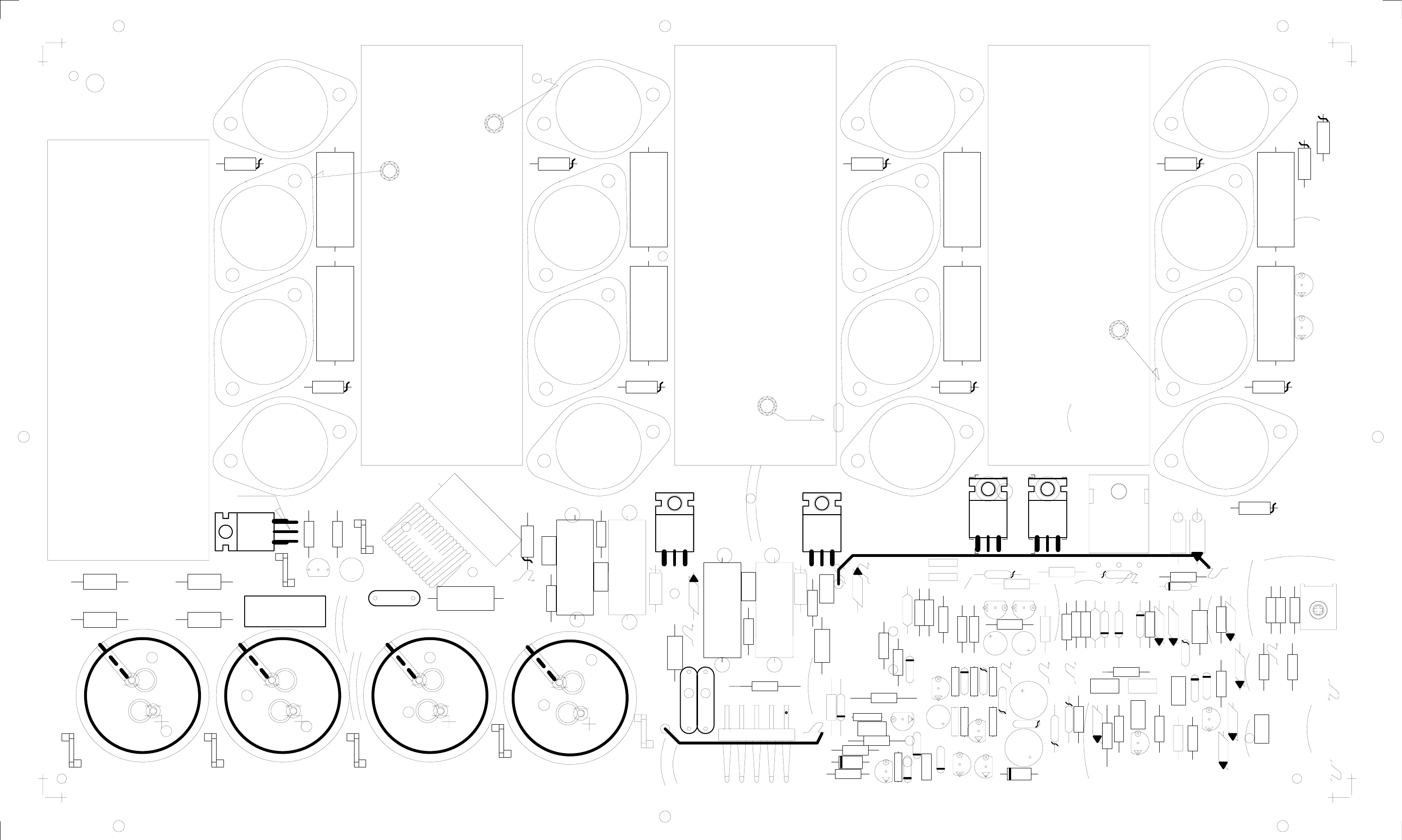
R27 2R2
GS
Q6A
@Q1
MTP2P50E
D1
4148
D24148
D3
4148
J12
R79
1W
0.R47
D9
4148
C22
@C3
#5892
80V
6800U
C23
@C3
#5892
80V
6800U
C24
@C3
#5892
80V
6800U
C25
@C3
#5892
80V
6800U
C3
22U
10V
TAB7
WC6
WC6
16AWG
5.5"BLK
R5
249R
R3
2R2
R4
2R2
R7
150R
R15 150R
R10
4K7
R8
15K
R9
249R
R19 249R
R16 15K
R14
39R
R13
36K
R610K0
R1
39R
R17
249R
R18
10K0
R2
68R
R37
@R3
27K
R38
@R3
27K
R39
@R2
91K
R67
@R4
0.5W
15K
1
R26 470R
R46 1K
R30
1K2
R31
47R
R47 39R
ZD10
4V7/1W
J3
R43
470R
R20 3K
R73 100K
D11
BAV21
J22
TAB6
TAB4
R64
33K
R65
10R
Q1
BC550
Q4
BC550
Q2
BC560
Q3
BC560
Q9
BC550
Q10
BC560
Q8
BC550
RT1
4K7
VBE
C2
1N
C4 470P
R63
5R6
5WATT
TAB3TAB1
GS
Q11
MTP10N15L
GS
Q12
@Q3
MTP8P20
C18
10N
J16
R74 150K
ZD9
16V/1W
ZD8
16V/1W
C1
1N5
C15
2N2
#5427
500V
C9
2N2 #5427
500V
C10
680P
C16
470P
C12
22N
C13
22N
WC7
16AWG
7"YEL
TAB2
R45A
3K6
C26
22N
R28
1R
0.5W
R44
1R
0.5W
R52
0R15
¢
5WATT
R53
0R15
5WATT
R57
0R1
5WATT
R56
0R1
5WATT
R59
0R1
5WATT
R58
0R1
5WATT
R61
0R1
5WATT
R60
0R1
5WATT
R29
@R5
5WATT
3K6
R45
@R5
5WATT
3K6
Q22
YS#6927
.
Q24
YS#6927
.
R66
@R4
0.5W
15K
Q26
YS#6927
.
Q21
YS#6927
.
Q28
YS#6927
.
Q13
YS#6900
.
Q14
YS6900
.
Q16 YS#6900
.
Q18
YS#6900
.
Q20
YS#6900
.
D4
4148
Q23
YS#6927
.
Q27
YS#6927
.
D15
MR854
D14
MR854
D13
MR854
D12
MR854
D21
MR854
D19
MR854
D18
MR854
D17
MR854
D16
MR854
D22
MR854
TP2
D23
MR854
ZD4
12V
ZD3
3V
C17
100N
D26
4004
J19
ZD2
16V
C6
330U
16V
C7
330U
16V
Q7
2N6517
C11
220N
250V
Q30
TRIAC
MAC224-4
DC_PROT
J9
D25
4148
R62
3R9
2WATT
TP4
D24
4004
TP5
TP7
TP6
TP8
TP9
TP10
TP1
J20
R21
2K2
R76
8K2
ZD6
3V
ZD5
12V
D5
4148
R77
470K
R23
4K7
R24
220K R25
220K
R42
4K7
R22 3K
R75 150K
ZD7 18V
D28
4148
D27
4148
J1 R51
220R0
R35 1K
J4
R33
1W_FP
1R
R49
1WATT
0.R47
C27
22N
GS
Q6B
@Q1
MTP2P50E
ZD1
16V
C21
10U
16V
D10
BAV21
R72
@R6
47R
D7
4148
@Q1
J21
R49A
@R1
2R2
R29A
3K6
R49B
@R1
2R2
C5
22U
10V
Q5
@Q2
MTW10N40E
J15
Q15 YS#6900
.
Q17
YS#6900
.
Q25
YS#6927
.
TAB5
R78 470K
Q19
YS#6900
.
MC1
PART#
FUNCTION
J18
J17
R12
39R
Q29
MBS4992
L1
4uH
Q34
MPSA42
R40 1K
_WC7
C14
220N
250V
J7
J8
J6
J5
D20
MR854
J10
R35A
20K
R36
91K
R70
18K
R71
@R6
47R
J2
R48
39R
R68
@R4
0.5W
15K
RV1
100K
J11
R40A
20K
Q32
BC550
R69
@R4
0.5W
15K
R34 270R
C19
10N
250V
R50 270R
R55
220R0
Q33
2N5551
C8
2U2
10V
Q31
MPSA92
1
3
2
R32
39R
R11 22R
R41 2R2
ASSEMBLY M1002-9.00 BLANK SIZE=14.750"X8.850"PCB MECH M1002-9.00
NOTE #6
-
OUTPUT
+
OUTPUT
HOLE
AUTO ADJUST
TO M1011
VER. 9.10
RED WIRE
WIRE
BLUE
+78V
+145V GND
-78V -145V
1/2W
1/2W
1/4WATT
1/4WATT
AP-3400
M1002A
SGGS
AP-3400M1002A
P:\1002APRT.PRN
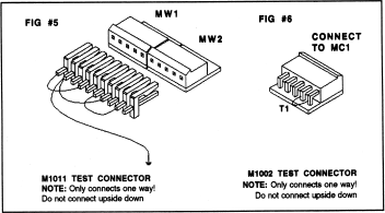
Testing Repaired Circuit Board
Now that you have rebuilt the M1002 or M1002A circuit board. It is just as important to
properly power up the board. If the sinewave doesn’t look right check the signal at test
point (1) on M1002 to ensure that the voltage amplifier on board M1011 or M1011A isn’t
distorting the signal. If there is still a damaged part on the board instantly turning it on
could blow up the board and you would be back where you started.
The best method is to connect the test connector shown in figure 3 to the 5 pin molex
connector MC1 and connect the power wires and ground to the power supply.
Connect a digital multimeter to test pins 8 and 9 to measure the bias quiescent current and
place a scope probe on the speaker output. Be sure to turn the quiescent current trimpot
RT1 fully counter clockwise.
Now using a variac slowly turn up the AC main voltage while monitoring the quiescent
voltage and the speaker output trace on the scope. Watching these two test points is a
good indicator of the health of the board. If you have a second multimeter connect it up
from the speaker output to test point 4 or 5. As you variac up also check these DC battery
voltages to ensure that they both increase in voltage to approximately +14 or –14 vdc.
If the board looks OK after variacing up to 120vac then slowly turn up the bias (RT1
trimpot) to obtain 3 to 5 millivolts of bias voltage on test points 8 and 9.
Now power down the board; connect MC1 to circuit board M1011 and variac up the
whole amplifier. Check the speaker output with a 1KHZ sinewave with no load. If this
looks good place the minimum rated load (4 ohm for M1002A, 2 ohm for M1002) on the
speaker output and increase the sinewave amplitude to the point of clipping. If the signal
looks free of oscillation, place a short across the speaker posts. The amplifier should go
into protect mode after 1/10 of a second. Remove the short and the sinewave will appear
6 seconds later.
Reassemble the complete amplifier and run just clipping music or pink noise into the
minimum rated speaker load for that model of amplifier. Let the amplifier heat up for 20
minutes. This will check the thermal mounting of the transistors and for any weak parts
not caught during troubleshooting.
If the amplifier passes this test the product is ready to return to the customer.
Figure 3.
See details of figure 3 in service manual.

YORKVILLE SOUND
AP3000 AND AP3400 SERVICE
Quick Fix for M1002 and M1002A
To speed up the servicing of the AP3000 or
AP3400 on your bench, Yorkville Sound’s service
department has developed a method to replace the
components most likely to fail when a M1002/A
amplifier board requires service.
This Quick Fix kit contains the procedure,
assembly drawings, and components to perform
the Quick Fix to a M1002 or M1002A board.
It should be understood that the person using
this procedure knows how to test resistors, diodes,
and transistors to determine if they are defective.
This procedure is not intended to be a substitute
for one’s lack of electronic capability.
Before starting, look at the board for repair
and locate the version number. It is very
important that you follow the procedure for the
appropriate circuit board version number.
A complimentary service manual for the
AP3000 power amplifier is supplied with this
M1002KIT.
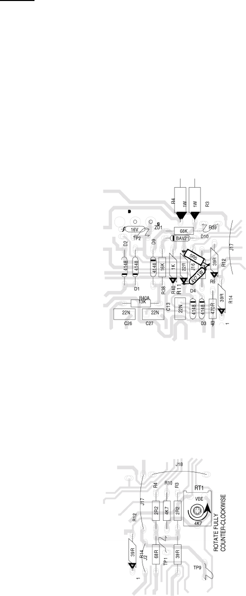
STEP 1. Locate the assembly drawing for the version number printed on
the M1002 or M1002A circuit board to be serviced.
2. Remove all of the transistors coloured RED on the assembly drawing.
3. Measure and remove any of the diodes coloured BLUE on the assembly
drawing that may be damaged. Replace a 1N4732A 1W 4V7 zener (#6459)
{These components already exist on version 9 and higher, add only in versions
9 and lower.] that may have been added to the component side of the board
along with a series 0.5 ohm resistor. Refer to figure 1.
Figure 1
4. Rotate the trim pot RT1 fully counter - clockwise as in figure 2. Inspect and
replace any resistors that look burnt. Measure all of the resistor values
coloured YELLOW on the assembly drawing. The value that you measure
may not be exactly what is shown on the assembly drawing but if the resistor
doesn’t look damaged it should measure within + or – 5% of the printed value.
Figure 2
5. Measure the resistor coloured GREEN. The measured value should measure
within + or – 5% value listed in the table below. Replace any resistor that
measured beyond the + or – 5% value listed in the table below.
Resistor Printed Correct
Number Value Measured Value
-5% +5%
R10 4K7 2K25 2K3 2K35
6. Measure across the pair of test points listed in the table below. If the
measured value is not within + or – 10% of the value listed in the table then
replace the resistors shown in the table below.
Test Layout Correct Replace
Points Reference Measured Value Resistors
A to A TP2 to J19 -10% +10% R11, R12, R14
15ohm 17 ohm 19 ohm
7. Measure the resistors coloured ORANGE. Since the value of these resistors is
0.1 ohm, your ohmmeter will measure the higher series resistance of the test
leads if the resistor is OK. If the resistor is damaged your ohmmeter will read a
very high resistance (an open circuit). Replace any damaged resistors.
8. Measure the output TO –3 transistors (Q13 to Q28) to determine if any are
damaged. Mark any damaged transistors with a marking pen.
9. Replace any output transistors that you have marked as being damaged.
Replace any diodes that you have found to be damaged. Replace all of the red
transistors that were removed.
10. Inspect the traces on the circuit board for any that have ‘fused’ open or look
like they got very hot. Bridge and solder a piece of wire over any damaged
traces.
AFTER YOU HAVE REPLACED ALL OF THE NECESSARY
COMPONENTS INSPECT THE REPAIRED BOARD FOR ANY
MISSING PARTS, CORRECT VALUES IN THE CORRECT
POSITION AND THAT ALL COMPONENTS ARE SOLDERED.
SHEARSHEAR
SHEAR SHEAR
VCD
SHEAR SHEAR
SHEARSHEAR
SOLDERSIDE M1002-9.00
BLANK SIZE=14.750"X8.850"
SGG
S
GS
DG
S
DG
GS
R27 2R2
GS
Q6A
@Q1
MTP2P50E
D1
4148
D24148
D3
4148
J12
R79
1W
0.R47
D9
4148
C22
@C3
#5892
80V
6800U
C23
@C3
#5892
80V
6800U
C24
@C3
#5892
80V
6800U
C25
@C3
#5892
80V
6800U
C3
22U
10V
TAB7
WC6
WC6
16AWG
5.5"BLK
R5
249R
R3
2R2
R4
2R2
R7
150R
R15 150R
R10
4K7
R8
15K
R9
249R
R19 249R
R16 15K
R14
39R
R13
36K
R610K0
R1
39R
R17
249R
R18
10K0
R2
68R
R37
@R3 27K
R38 @R3 27K
R39
@R2 91K
R67
@R4
0.5W
15K
1
R26 470R
R46
1K
R30
1K2
R31
47R
R47 39R
ZD10
4V7/1W
J3
R43
470R
R20
3K
R73 100K
D11
BAV21
J22
TAB6
TAB4
R64
33K
R65
10R
Q1
BC550
Q4
BC550
Q2
BC560
Q3
BC560
Q9
BC550
Q10
BC560
Q8
BC550
RT1
4K7
VBE
C2
1N
C4 470P
R63
5R6
5WATT
TAB3TAB1
GS
Q11
MTP10N15L
GS
Q12
@Q3
MTP8P20
C18
10N
J16
R74 150K
ZD9
16V/1W
ZD8
16V/1W
C1
1N5
C15
2N2
#5427
500V
C9
2N2 #5427
500V
C10
680P
C16
470P
C12
22N
C13
22N
WC7
16AWG
7"YEL
TAB2
R45A
3K6
C26
22N
R28
1R
0.5W
R44
1R
0.5W
R52
0R15
5WATT
R53
0R15
5WATT
R57
0R1
5WATT
R56
0R1
5WATT
R59
0R1
5WATT
R58
0R1
5WATT
R61
0R1
5WATT
R60
0R1
5WATT
R29
@R5
5WATT
3K6
R45
@R5
5WATT
3K6
Q22
YS#6927
.
Q24 YS#6927
.
R66
@R4
0.5W
15K
Q26
YS#6927
.
Q21
YS#6927
.
Q28
YS#6927
.
Q13
YS#6900
.
Q14
YS6900
.
Q16
YS#6900
.
Q18
YS#6900
.
Q20
YS#6900
.
D4
4148
Q23
YS#6927
.
Q27
YS#6927
.
D15
MR854
D14
MR854
D13
MR854
D12
MR854
D21
MR854
D19
MR854
D18
MR854
D17
MR854
D16
MR854
D22
MR854
TP2
D23
MR854
ZD4
12V
ZD3
3V
C17
100N
D26
4004
J19
ZD2
16V
C6
330U
16V
C7
330U
16V
Q7
2N6517
C11
220N
250V
Q30
TRIAC
MAC224-4
DC_PROT
J9
D25
4148
R62
3R9
2WATT
20
19
18
17
16
15
14
13
12
11
10
9
8
7
6
5
4
3
2
1
# DESCRIPTION OF CHANGEVER#DATE
MODEL(S):-
D
D
D
.
MAR/12/98
.
JAN/28/98
DEC/08/97
.
.
.
DEC/09/97
D
D
OCT/19/95
MAR/01/95
FEB/28/95
.
.
AUG/25/94
V
V
V
.
9.10
.
9.00
8.00
.
.
.
7.00
V
.
6.20
.
6.10
.
.
6.00
N
N
N
1R/1W->0.R47/1W_ZD7_20V-18V
PC#5656_R49_2X1R_1/4W->0.R47_1W_R79
=2X_1R_1/4W_IN_PARALLEL_BY_HAND
PC#5551_ADD_R79,ZD10_ACROSS_R11_R49
PC#5546_R36,R39_1_END_78V->145V_
.
.
.
PC#5546
.
.
PC#4924
.
.
PC#4531
PC#4650
PC#4645
AP-3400
M1002A.PCB_DATABASE_HISTORY
TP4
D24
4004
TP5
TP7
TP6
TP8
TP9
TP10
TP1
J20
R21
2K2
R76
8K2
ZD6
3V
ZD5
12V
D5
4148
R77
470K
R23
4K7
R24
220K R25
220K
R42
4K7
R22 3K
R75 150K
ZD7 18V
D28
4148
D27
4148
J1 R51
220R0
R35 1K
J4
R33
1W_FP
1R
R49
1WATT
0.R47
C27
22N
GS
Q6B
@Q1
MTP2P50E
ZD1
16V
C21
10U
16V
D10
BAV21
20
19
18
17
16
15
14
13
12
11
10
9
8
7
6
5
4
3
2
1
# DESCRIPTION OF CHANGEVER#DATE
MODEL(S):-
D
D
D
D
D
D
JAN/28/98
DEC/17/97
D
D
D
OCT/28/97
JAN/97
.
.
OCT/19/95
MAR/01/95
FEB/28/95
.
AUG/25/94
V
V
V
V
V
V
9.00
8.10
V
V
V
7.00
.
.
.
6.20
.
6.10
.
6.00
N
N
N
N
N
N
PC#5550_ADD_R79,ZD10_ACROSS_R11
PC#5550_R40A/R35A_16K->13K
.
.
.
PC#5498
ADDED_ROUTING_AT_TP8-TP9
N
N
PC#4924
N
N
PC#4650
PC#4645
AP-3000
M1002.PCB_DATABASE_HISTORY
R72
@R6
47R
D7
4148
@Q1
J21
R49A
@R1
2R2
R29A
3K6
R49B
@R1
2R2
C5
22U
10V
Q5
@Q2
MTW10N40E
J15
Q15 YS#6900
.
Q17
YS#6900
.
Q25
YS#6927
.
TAB5
R78 470K
Q19
YS#6900
.
MC1
PART#
FUNCTION
J18
J17
R12
39R
Q29
MBS4992
L1
4uH
Q34
MPSA42
R40 1K
_WC7
C14
220N
250V
J7
J8
J6
J5
D20
MR854
J10
R35A
20K
R36
91K
R70
18K
R71
@R6
47R
J2
R48
39R
R68
@R4
0.5W
15K
RV1
100K
J11
R40A
20K
Q32
BC550
R69
@R4
0.5W
15K
R34 270R
C19
10N
250V
R50 270R
R55
220R0
Q33
2N5551
C8
2U2
10V
Q31
MPSA92
1
3
2
R32
39R
R11 22R
R41 2R2
ASSEMBLY M1002-9.00 BLANK SIZE=14.750"X8.850"PCB MECH M1002-9.00
8
7
R11,12,14,33,TO FLAMEPROOF. CIRCUIT CHANGES
R37,R38 10K->27K,R36,R39 27K->91K R34,R50 249R
R55,R51 249R->220R0 R40A,R35A 470R->20K
R11,12,14,33,49 TO FLAMEPROOF. CIRCUIT CHANGES ->270R C26,C27 10u->22N,R52,R53 0R1->0R15->270R C26,C27 10u->22N,R52,R53 0R1->0R15
R37,R38 8K2->16K,R36,R39 36K->68K R34,R50 249R
R55,R51 249R->220R0 R40A,R35A 470R->16K
NOTE #6
PT#6923 FROM MTP2P45 TO MTP2P50E
ACCOMODATE NEWER AND SMALLER FILTER CAPS ACCOMODATE NEWER AND SMALLER FILTER CAPS
TABS ADDED FOR SPKR OUTPUTS RTV HOLES MOVED TO TABS ADDED FOR SPKR OUTPUTS RTV HOLES MOVED TO
ADD DON’T BLOW ME UP CIRCUIT ADD DON’T BLOW ME UP CIRCUIT
REPLACE EYELETS WITH TABS REPLACE EYELETS WITH TABS
ROBOT ASSEMBLY. CHANGES TO TRACE ONLY
COLLECTORS MADE LARGER TO ACCOMODATE COLLECTORS MADE LARGER TO ACCOMODATE
PAD SIZE FOR OUTPUT TRANSISTOR PAD SIZE FOR OUTPUT TRANSISTOR
-
OUTPUT
+
OUTPUT
HOLE
AUTO ADJUST
TO M1011
VER. 9.10
RED WIRE
WIRE
BLUE
+78V
+145V GND
-78V -145V
1/2W
1/2W
1/4WATT
1/4WATT
AP-3400
M1002A
SGGS
AP-3400M1002A
A
CHECK
CHECK
CHECK
CHECK
CHECK
CHECK
CHECK
CHECK
CHECK
CHECK
CHECK
CHECK
CHECK
CHECK
CHECK
CHECK
BLU
RED
BLU
GREY
YELLOW
WHITE
YEL
WHT
RED
FAN-
BLK
T-BRK
BLK
RED
YELLOW
BLU
AC-WHITE
FAN-
L1
WC7
C44
C45
C46
C47
EY7
EY10
EY11
EY5
EY12
WC8
TJH1
WC10
WC4
WC3
EY13
WC1
WC11
WC6
EY8
EY6
EY9
RV5
100K
EY2
EY3
EY4
C55
4N7
250V
EY14
C53
22N
250V
C54
22N
250V
RV6
100K
#1289
AP-3400CE XFMR WIRING
NOV 13. 95
SHOWN WIRED FOR
230V
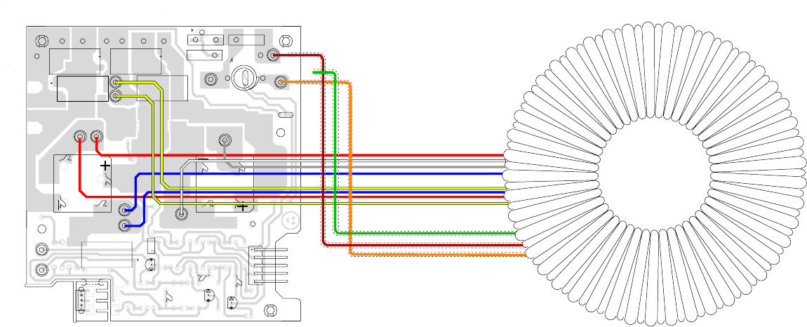
BLU
RED
BLU
GREY
YELLOW
WHITE
YEL
WHT
RED
FAN-
BLK
T-BRK
BLK
RED
YELLOW
BLU
AC-WHITE
FAN-
L1
WC7
C44
C45
C46
C47
EY7
EY10
EY11
EY5
EY12
WC8
TJH1
WC10
WC4
WC3
EY13
WC1
WC11
WC6
EY8
EY6
EY9
RV5
100K
EY2
EY3
EY4
C55
4N7
250V
EY14
C53
22N
250V
C54
22N
250V
RV6
100K
#1289
AP-3400CE XFMR WIRING
NOV 13. 95
SHOWN WIRED FOR
245V
