ZTE ME3630 LTE Module User Manual
ZTE Corporation LTE Module
UserManual.wiki
>
ZTE
>
ME3630 User Manual
Users Manual
Navigation menu
Upload a User Manual
Namespaces
Wiki Guide
HTML
PDF
Info
Views
User Manual
Discussion / Help
Navigation
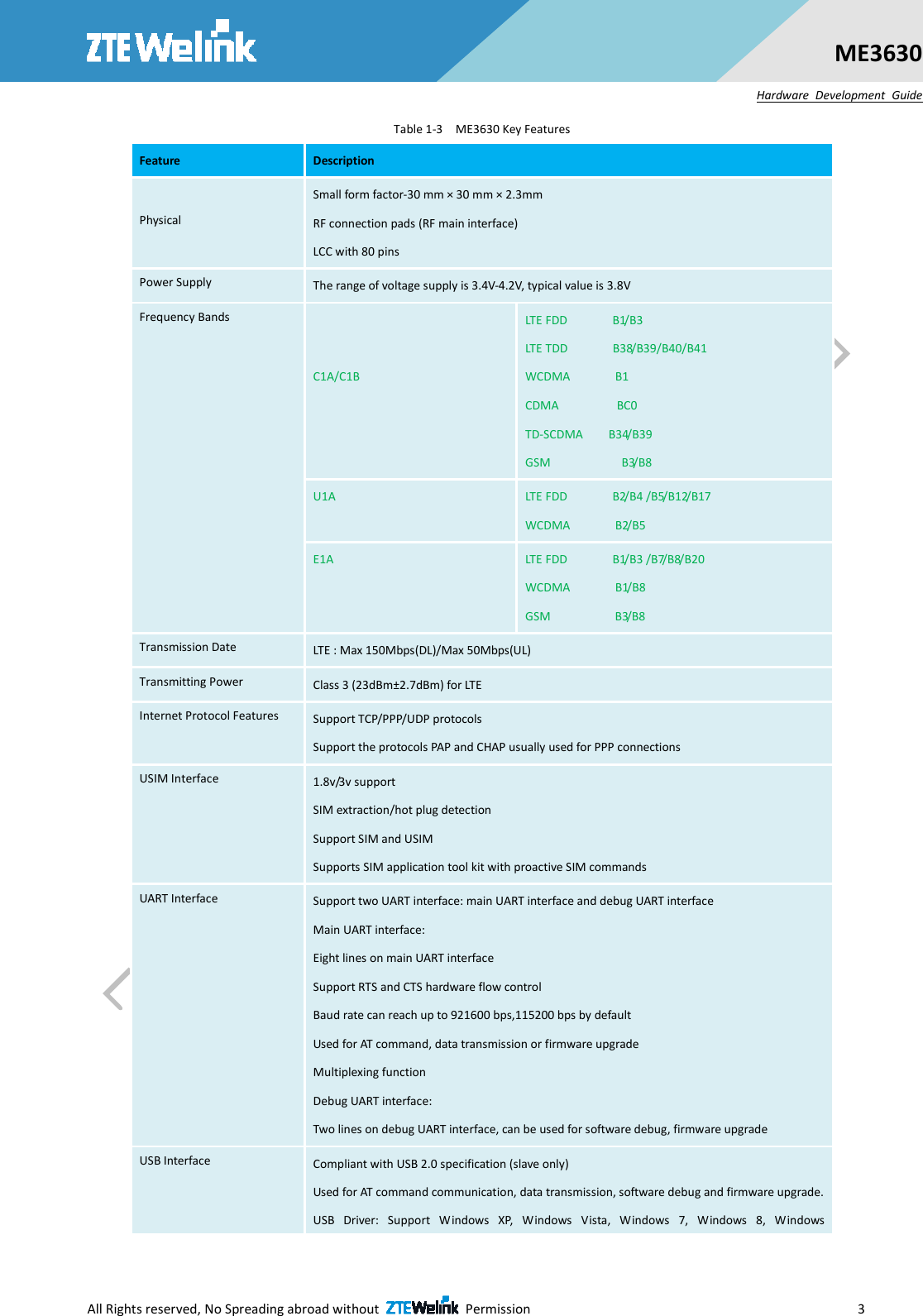
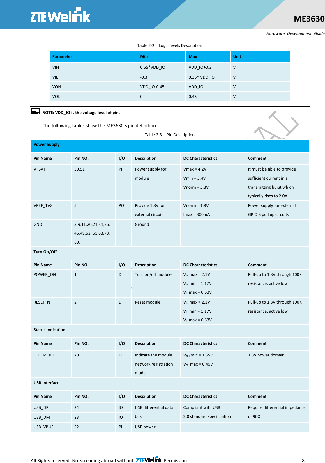
![All Rights reserved, No Spreading abroad without Permission VIII ME3630 Hardware Development Guide TABLES Table 1-1 ME3630 Reference Using Area .................................................................................................................................................. 1 Table 1-2 ME3630 Supported Band ........................................................................................................................................................... 1 Table 1-3 ME3630 Key Features ............................................................................................................................................................. 3 Table 2-1 IO Parameters Definition ........................................................................................................................................................ 7 Table 2-2 Logic levels Description ........................................................................................................................................................... 8 Table 2-3 Pin Description ........................................................................................................................................................................ 8 Table 2-4 Power Supply ........................................................................................................................................................................ 13 Table 2-5 POWER_ON/OFF Pin Description .......................................................................................................................................... 14 Table 2-6 Power-on Time...................................................................................................................................................................... 15 Table 2-7 Pin Definition of the USIM Interface ..................................................................................................................................... 15 Table 2-8 Pin Description of Molex USIM Card Holder ......................................................................................................................... 17 Table 2-9 Pin Description of Amphenol USIM Card Holder .................................................................................................................. 18 Table 2-10 USB Pin Description ............................................................................................................................................................ 19 Table 2-11 Pin Definition of the Main UART Interface .......................................................................................................................... 20 Table 2-12 Pin Definition of the Debug UART Interface ....................................................................................................................... 20 Table 2-13 Pin Definition of Network Indicator .................................................................................................................................... 22 Table 2-14 Working State of the Network Indicator ............................................................................................................................. 22 Table 2-15 Pin Definition of the ADC .................................................................................................................................................... 22 Table 2-16 Characteristic of the ADC .................................................................................................................................................... 23 Table 2-17 Pin Definition of WAKEUP_OUT .......................................................................................................................................... 23 Table 2-18 Pin Definition of GPIO ......................................................................................................................................................... 23 Table 3-1 Pin Definition of GPIO ........................................................................................................................................................... 24 Table 4-1 Absolute Maximum Ratings .................................................................................................................................................. 27 Table 4-2 Operating Temperature ........................................................................................................................................................ 27 Table 4-3 Averaged standby DC power consumption [1] ..................................................................................................................... 27 Table 4-4 Averaged standby DC power consumption [2] ..................................................................................................................... 27 Table 4-5 Averaged standby DC power consumption [3] ..................................................................................................................... 28 Table 4-6 Conducted RF Output Power ................................................................................................................................................ 28 Table 4-7 Conducted RF Receiving Sensitivity [1] ................................................................................................................................. 28 Table 4-8 Conducted RF Receiving Sensitivity [2] ................................................................................................................................. 28 Table 4-9 GNSS Technical Parameters .................................................................................................................................................. 29 Table 4-10 ESD ...................................................................................................................................................................................... 29 Table 6-1 Testing Standard ................................................................................................................................................................... 33 Table 6-2 Testing Environment ............................................................................................................................................................. 34 Table 6-3 Testing Instrument & Device ................................................................................................................................................ 34 Table 6-4 Reliability Features ............................................................................................................................................................... 35 Table 7-1 Baking parameters ................................................................................................................................................................ 36 Table 7-2 LCC module PAD’s steel mesh opening ................................................................................................................................. 36](https://usermanual.wiki/ZTE/ME3630/User-Guide-3093421-Page-9.png)
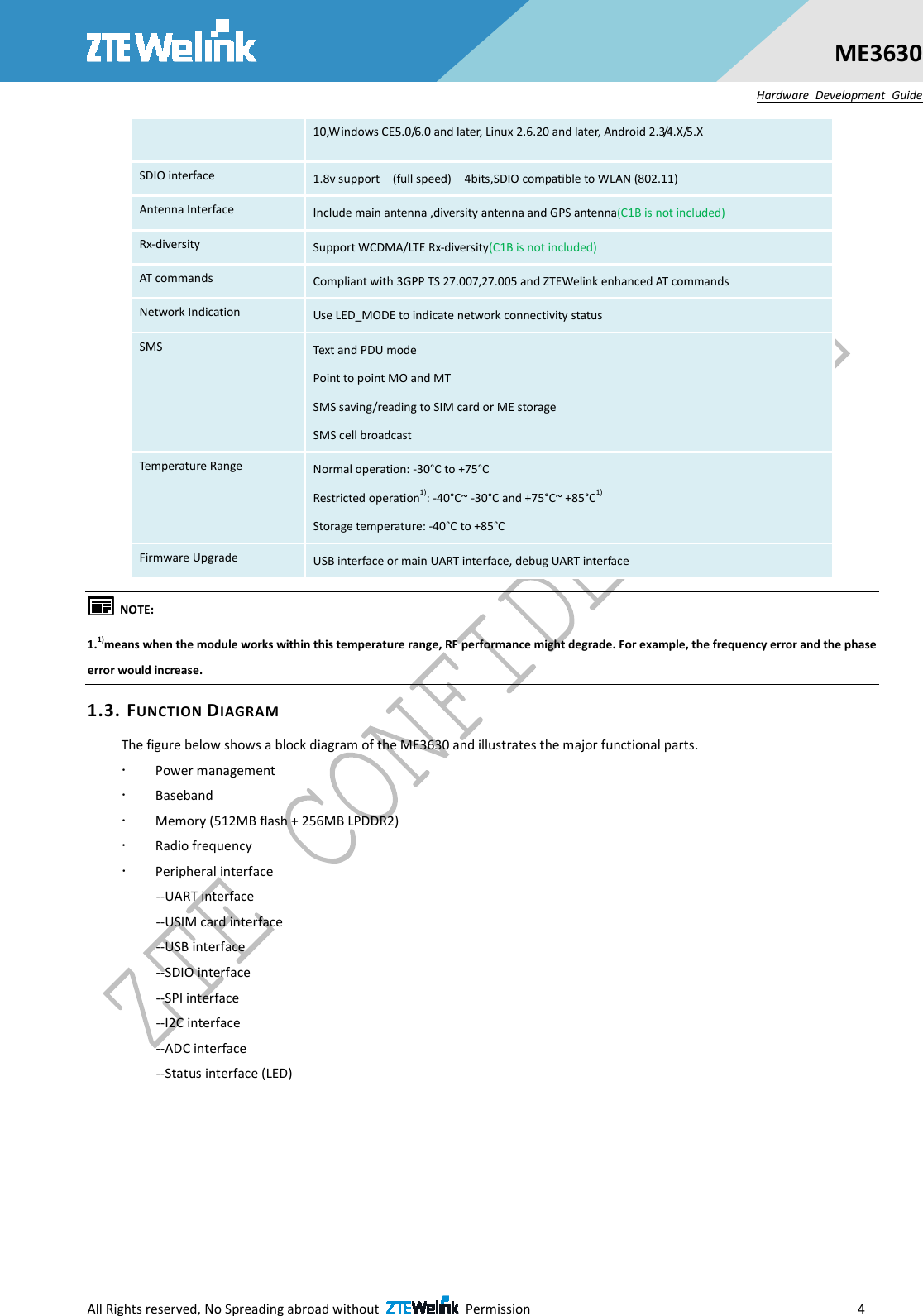
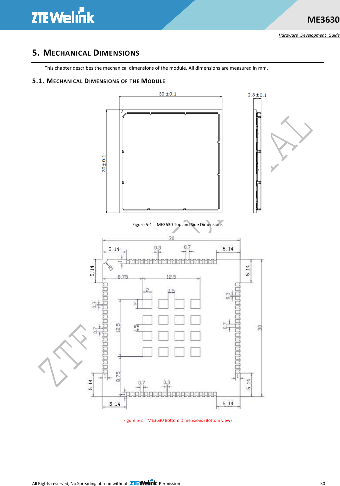
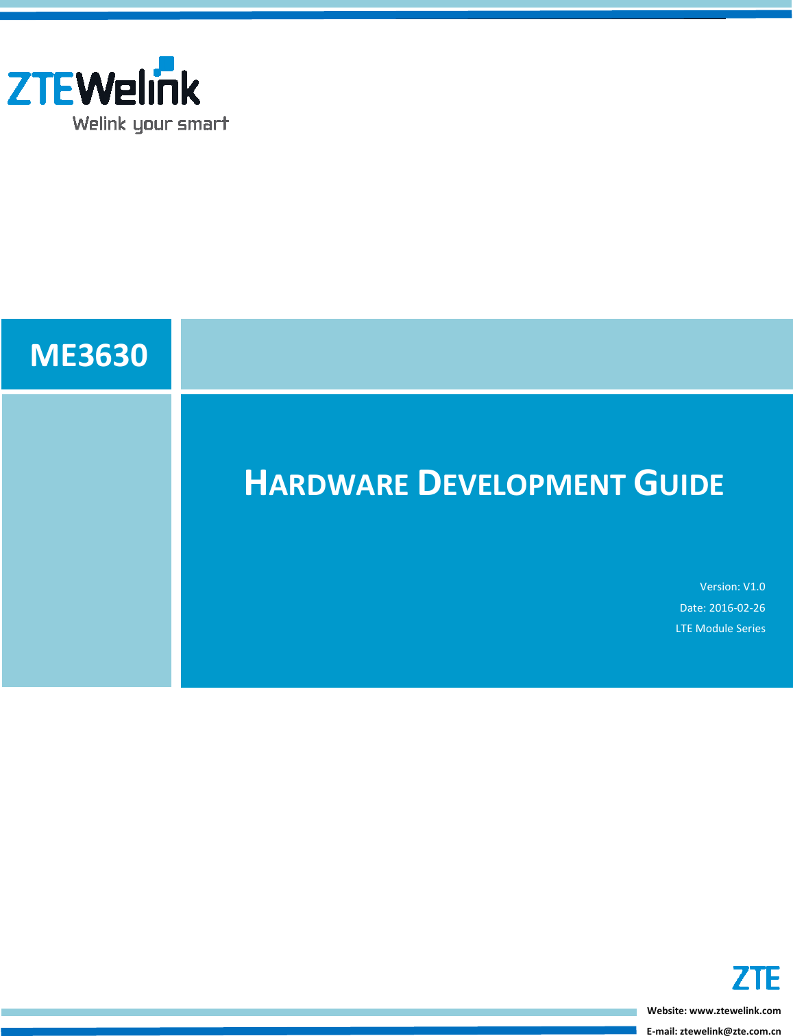
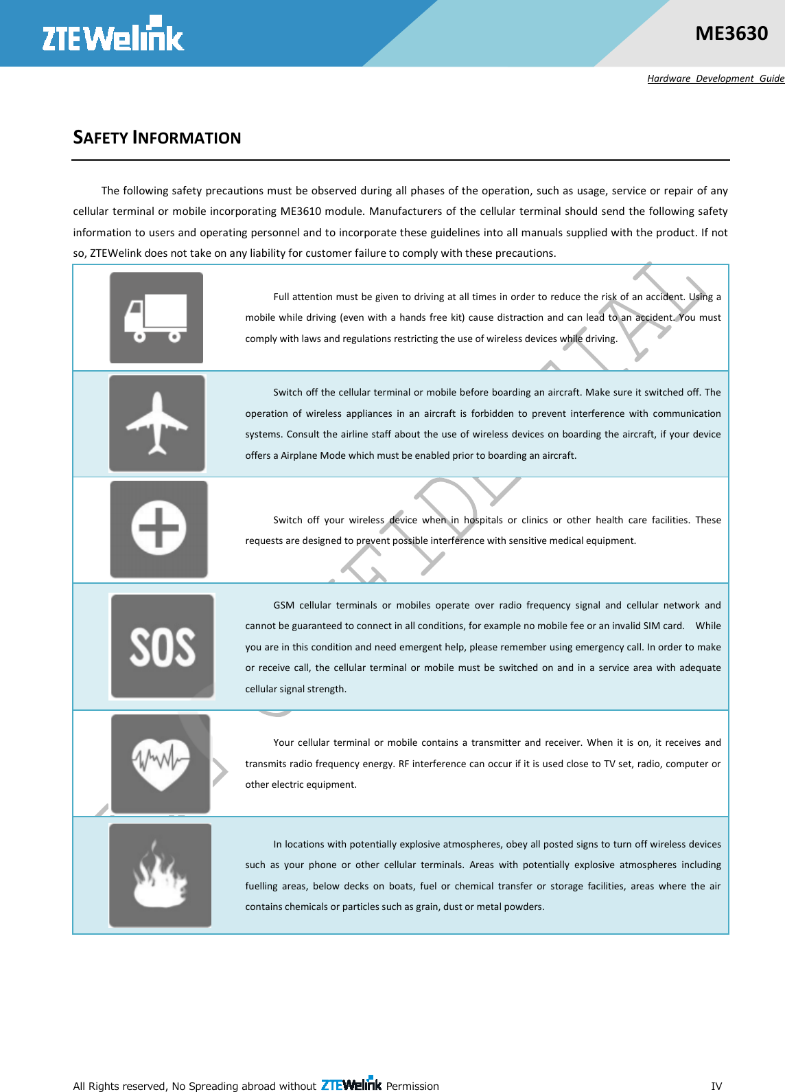
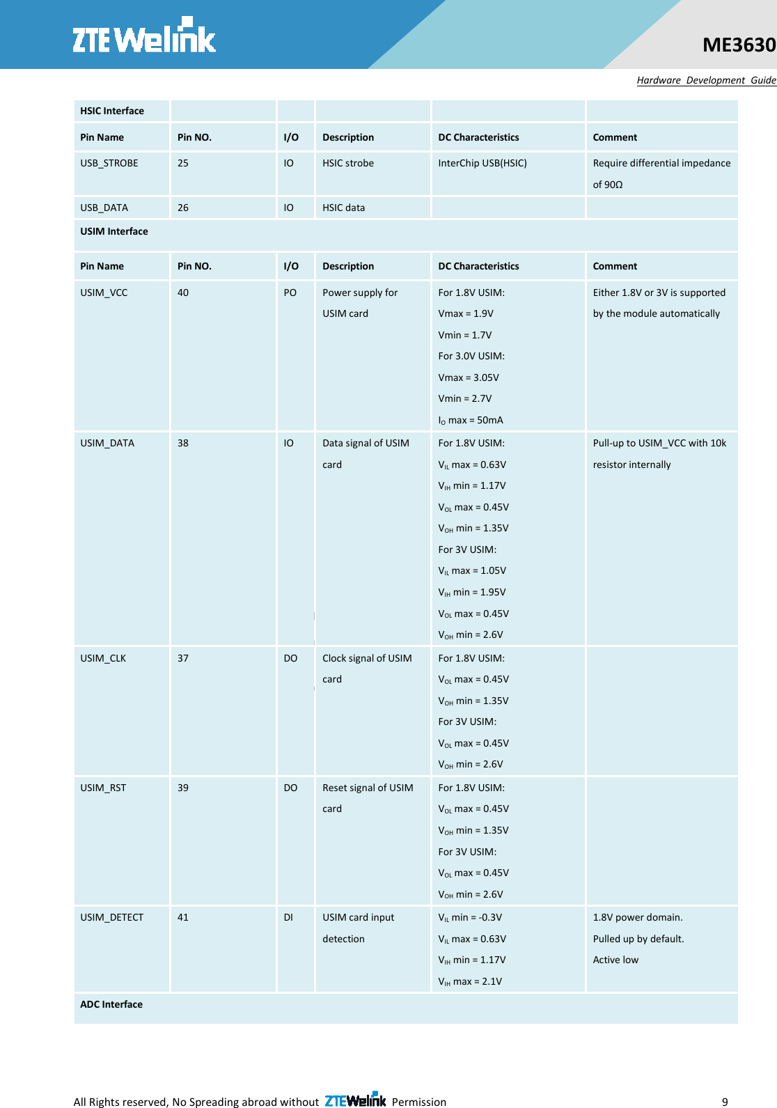
![All Rights reserved, No Spreading abroad without Permission 5 ME3630 Hardware Development Guide Figure 1-1 System Connection Structure 1.4. EVALUATION BOARD In order to help you to develop applications with ME3630, ZTEWelink supplies an evaluation board (G2000), RS-232 to USB cable, USB data cable, power adapter, antenna and other peripherals to control or test the module. For details, please refer to the related document [ZTEWelink G2000 Dev Board User Guide_V1.2].](https://usermanual.wiki/ZTE/ME3630/User-Guide-3093421-Page-15.png)
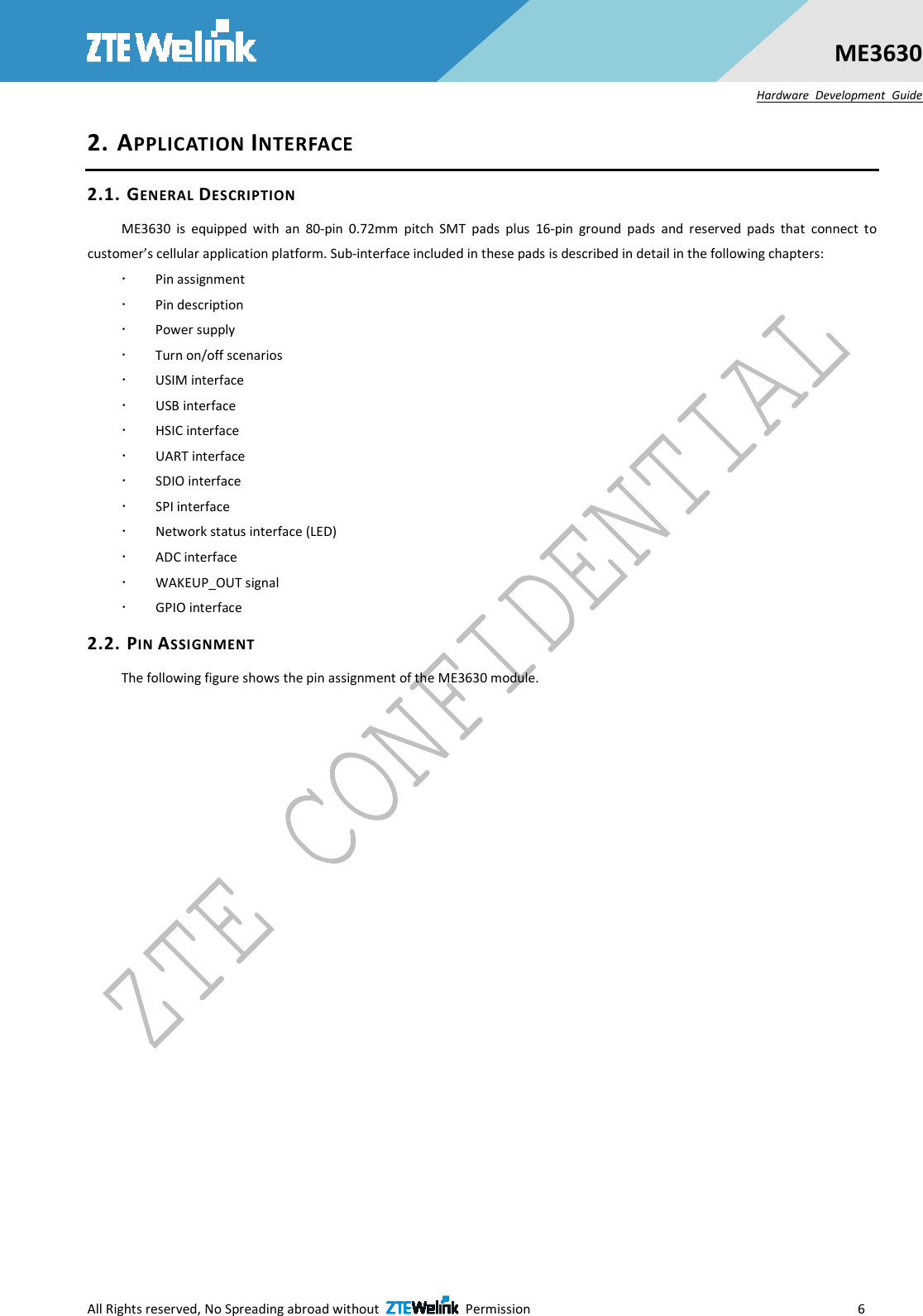
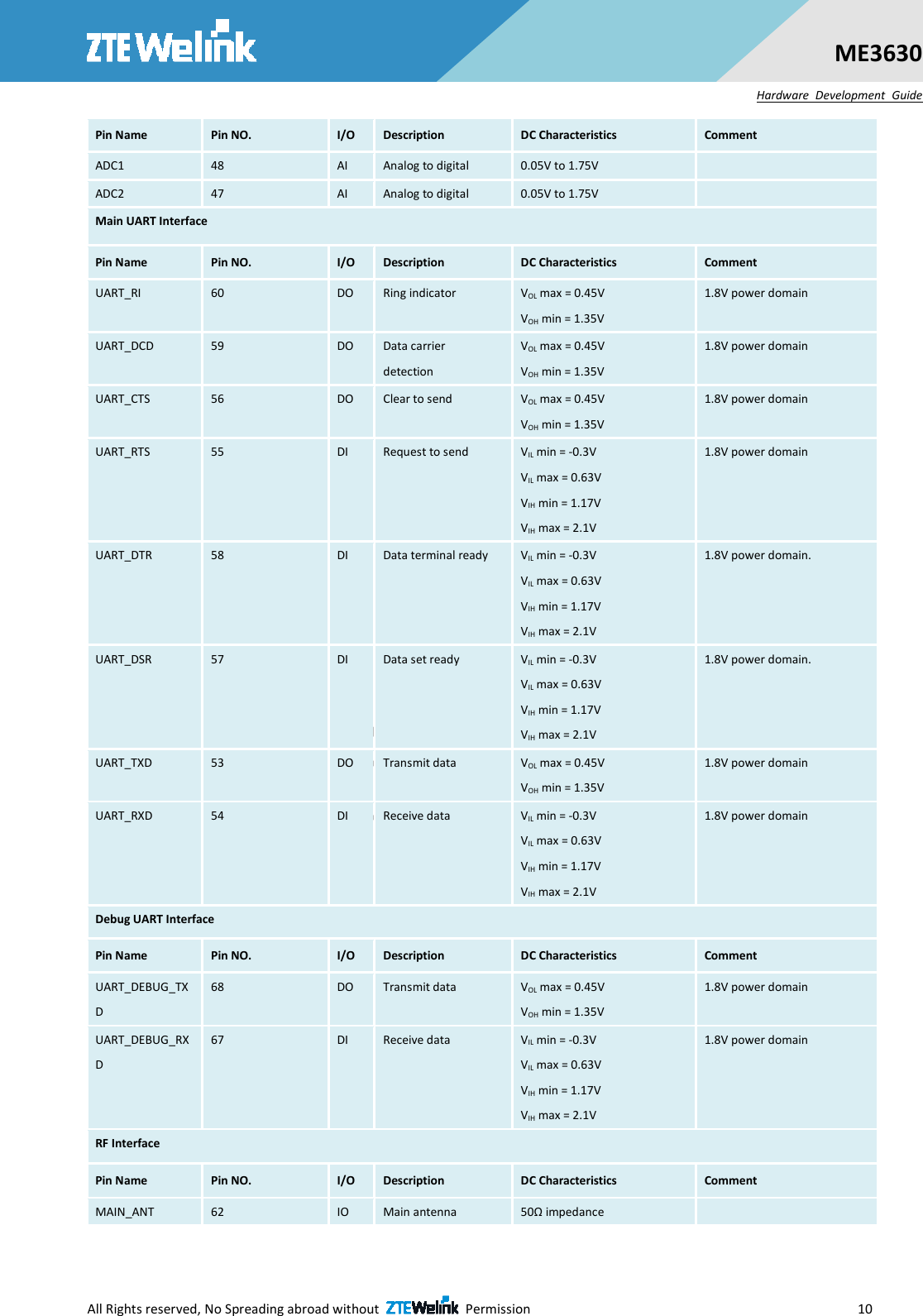
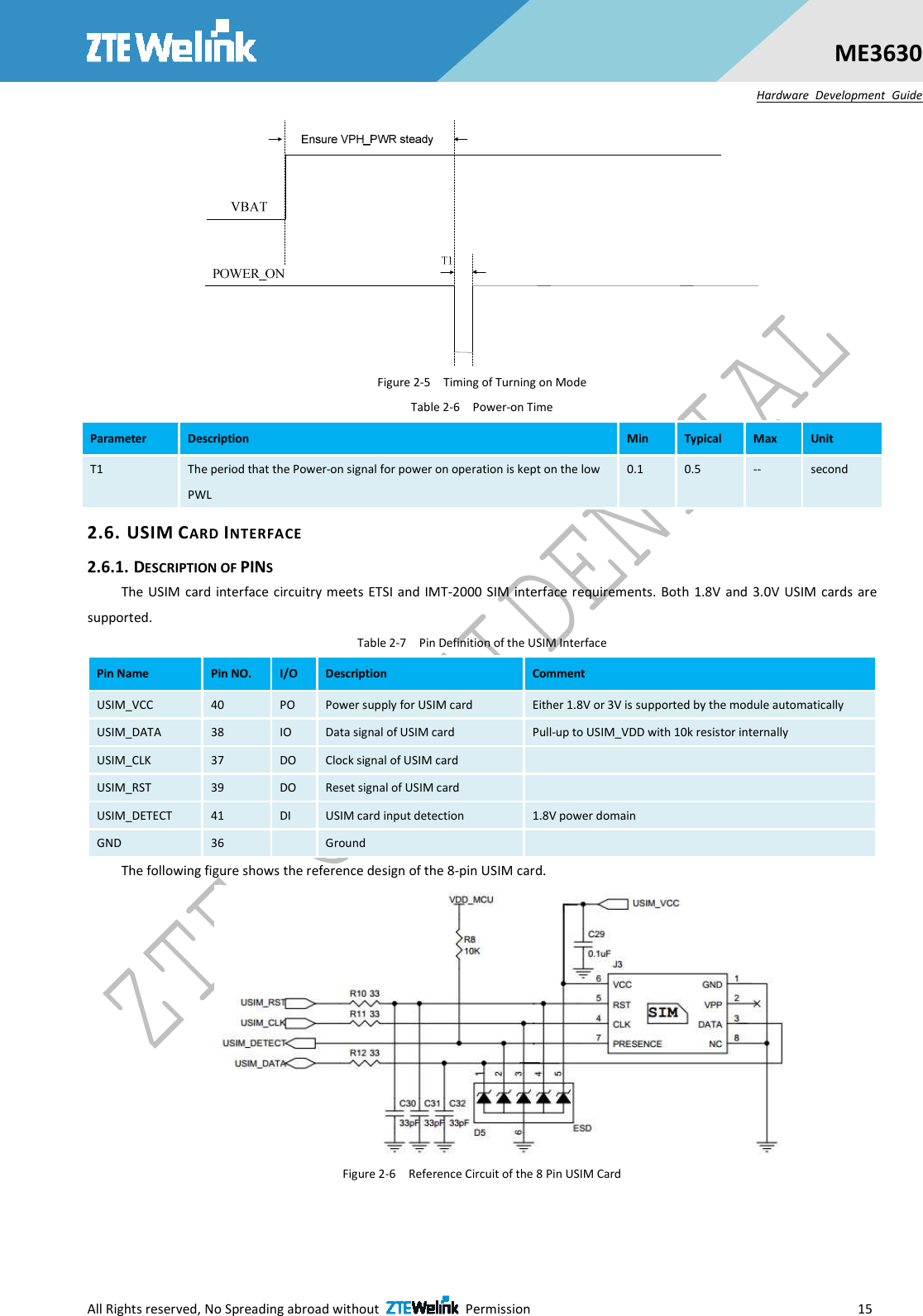
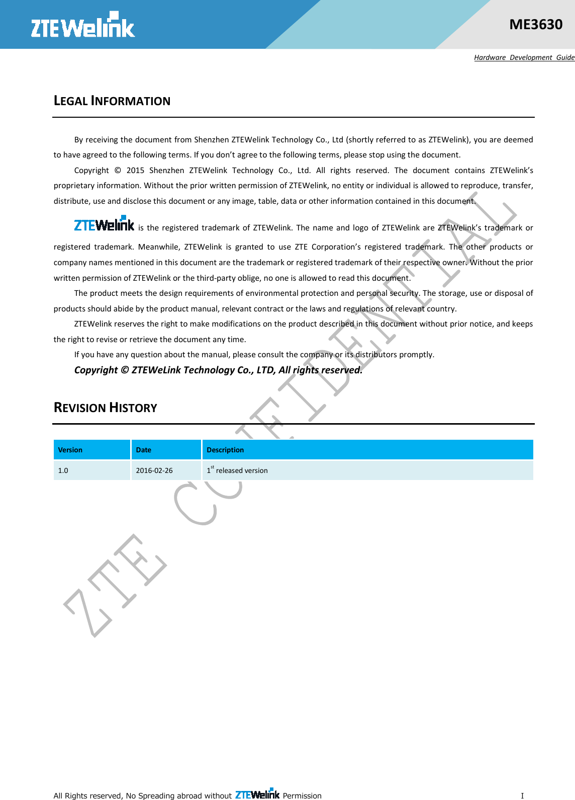
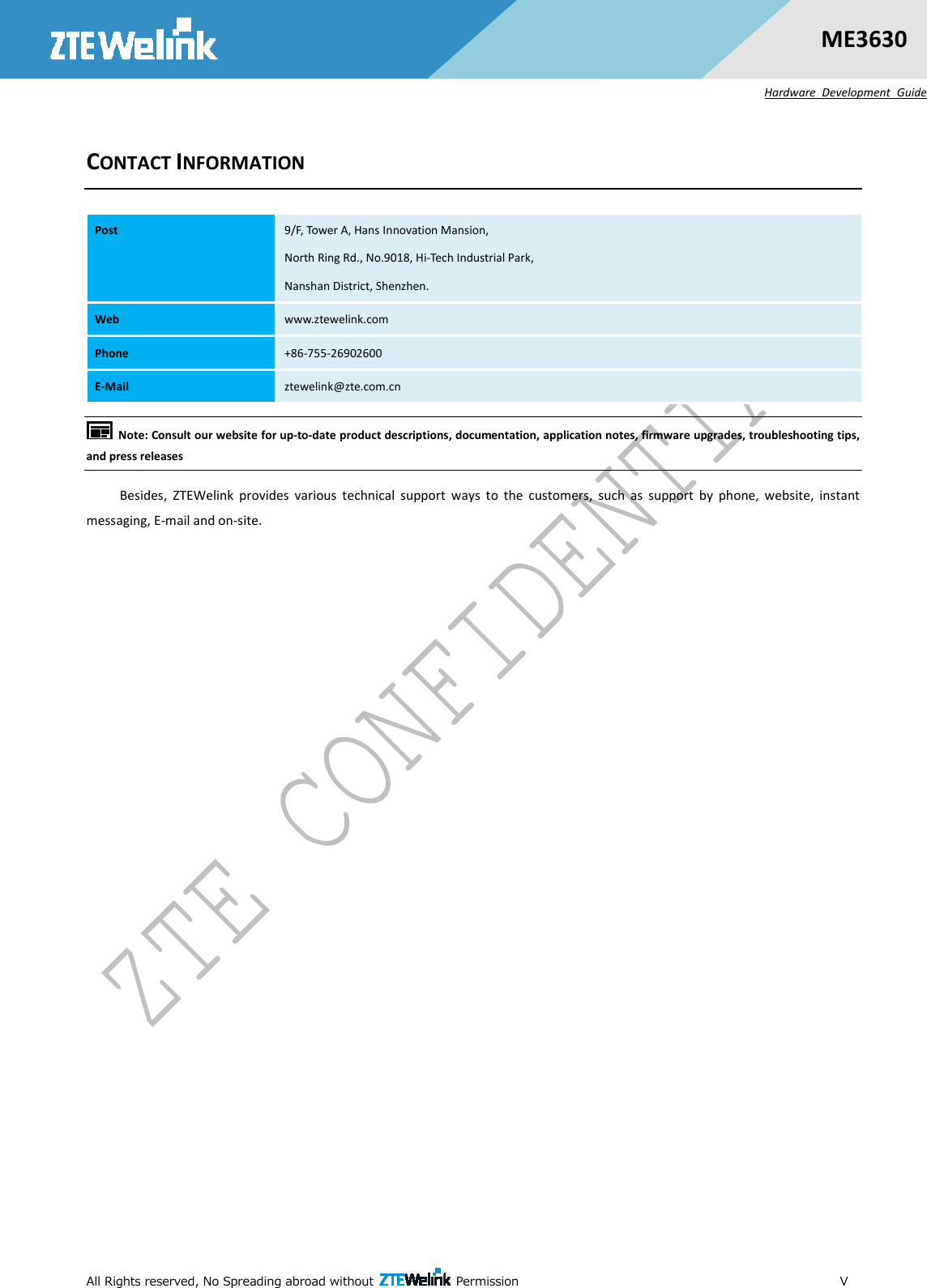
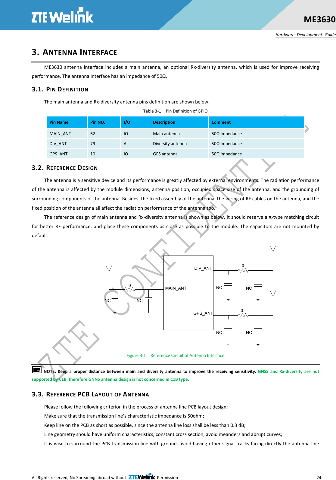
![All Rights reserved, No Spreading abroad without Permission 16 ME3630 Hardware Development Guide NOTES: 1. R10~R12 and D5 are applied to suppress the EMI spurious transmission and enhance the ESD protection.Should be closed to J3. 2.USIM_DETECT is used to detect USIM card, which will be low when the USIM card is inserted. 3.The value of C29 shoule be less than 1uF 4.USIM_DETECT is 1.8V power domain,VDD_MCU should be 1.8V. ME3630 supports USIM card hot-plugging via the USIM_ DETECT pin. For details, refer to document [ME3630_AT_Commands_Manual_V1.0]. If you do not need the USIM card detect function, keep USIM_ DETECT unconnected. The reference circuit for using a 6-pin USIM card socket is illustrated as the following figure. Figure 2-7 Reference Circuit of the 6 Pin USIM Card NOTES: 1. R14~R16 and D6 are applied to suppress the EMI spurious transmission and enhance the ESD protection.D6 should be closed to J4 2.The value of C33 shoule be less than 1uF. In order to enhance the reliability and availability of the USIM card in customer’s application, please follow the following criterion in the USIM circuit design: Keep layout of USIM card as close as possible to the module. Assure the possibility of the length of the trace is less than 50mm. Keep USIM card signal away from RF and V_BAT alignment. Assure the ground between module and USIM cassette short and wide. Keep the width of ground and USIM_VCC no less than 0.5mm to maintain the same electric potential. The decouple capacitor of USIM_VCC should be less than 1uF and must be near to USIM cassette. To avoid cross-talk between USIM_DATA and USIM_CLK, keep them away with each other and shield them with surrounded ground. In order to offer good ESD protection, it is recommended to add TVS such as WILL (http://www.willsemi.com) ESDA6V8AV6. The 33Ω resistors should be added in series between the module and the USIM card so as to suppress the EMI spurious transmission and enhance the ESD protection. Please note that the USIM peripheral circuit should be close to the USIM card socket. The pull-up resistor on USIM_DATA line can improve anti-jamming capability when long layout trace and sensitive occasion is applied.](https://usermanual.wiki/ZTE/ME3630/User-Guide-3093421-Page-26.png)
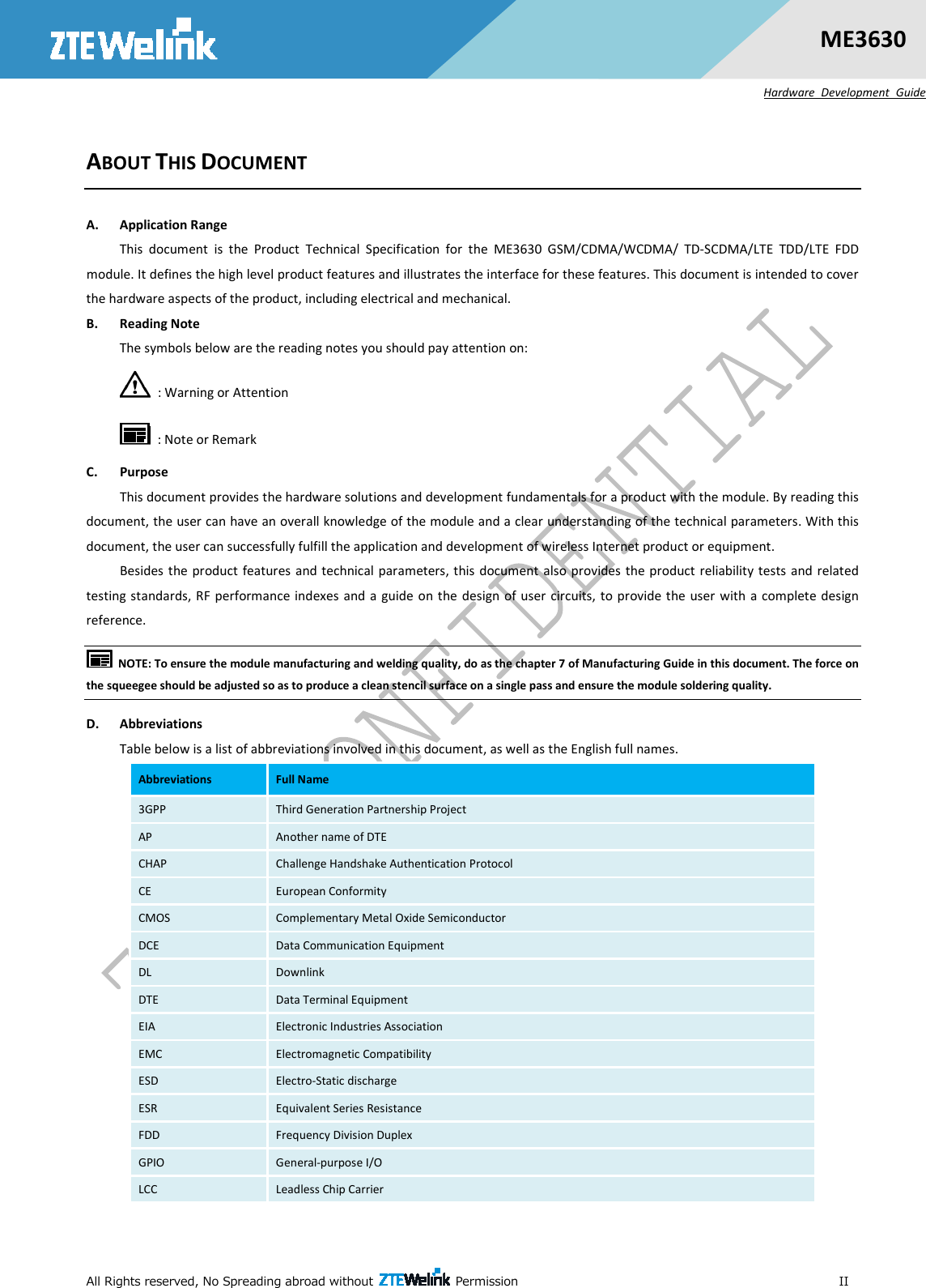
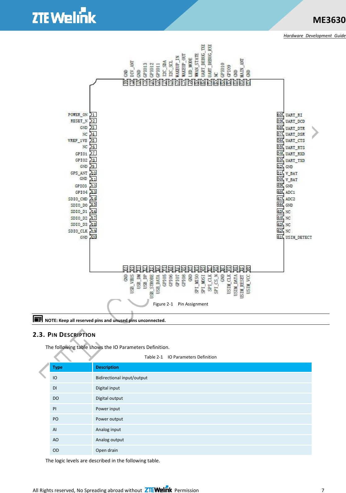
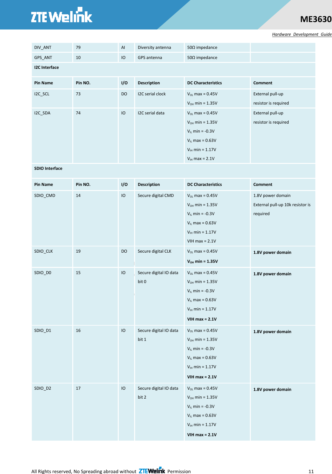
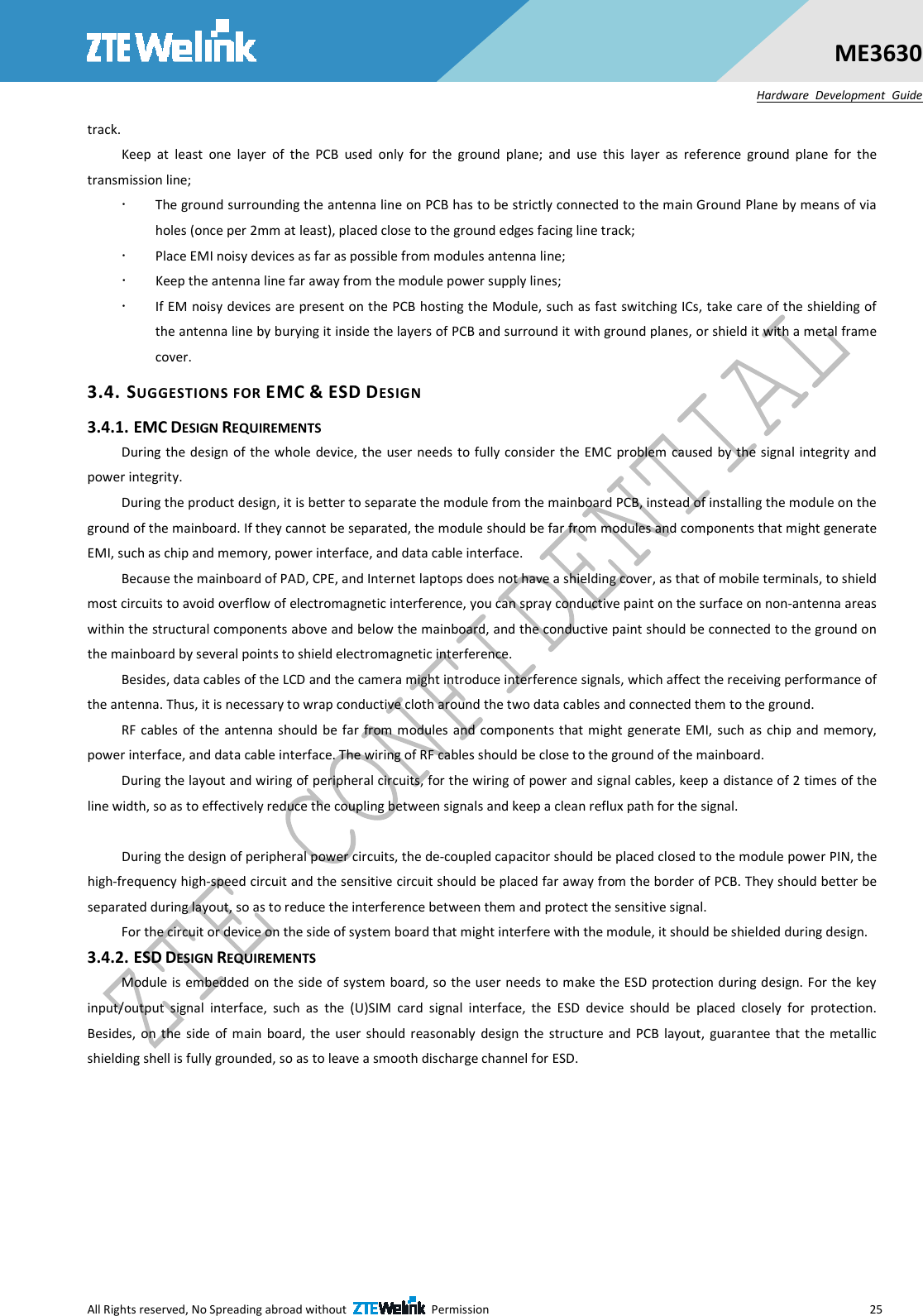
![All Rights reserved, No Spreading abroad without Permission 22 ME3630 Hardware Development Guide Debugging UART port is a 2-wire interface. It should be connected with its test point or jumper pin during design. 2.9. NETWORK STATUS INDICATION The network indication pin LED_MODE can be used to drive a network status indicator LED. The different modes of status indicator flashing indicate different network statuses. The following tables describe pin definition and logic level changes in different network status. Table 2-13 Pin Definition of Network Indicator Pin Name Pin NO. I/O Description Comment LED_MODE 70 DO Indicate the module network registration mode 1.8V power domain Table 2-14 Working State of the Network Indicator LED Status Module status High level, LED on Module is in the standby mode Low level 1.8s(LED off), High level 0.2s(LED on) PDP activated, and get the IP address Low level 0.2s(LED off), High level 1.8s(LED on) Socket established(when using External protocol stack, $MYSOCKETLED should be sent by CMUX to control the LED) Figure below is the reference circuit design diagram. Figure 2-16 Reference Circuit of the Network Indicator 2.10. ADC INTERFACE The module provides two ADCs to digitize the analog signal to 10-bit digital data such as battery voltage, temperature and so on. Using AT command “AT+ZADC1?” can read the voltage value on ADC1 pin. Using AT command “AT+ZADC2?” can read the voltage value on ADC2 pin. The read value is expressed in mV. For more details of these AT commands, please refer to document [ME3630_AT_Commands_Manual_V1.0]. In order to improve the accuracy of ADC, the trace of ADC should be surrounded by ground. Table 2-15 Pin Definition of the ADC Pin Name Pin NO. Description ADC1 48 General purpose analog to digital converter. ADC2 47 General purpose analog to digital converter. The following table describes the characteristic of the ADC function.](https://usermanual.wiki/ZTE/ME3630/User-Guide-3093421-Page-32.png)
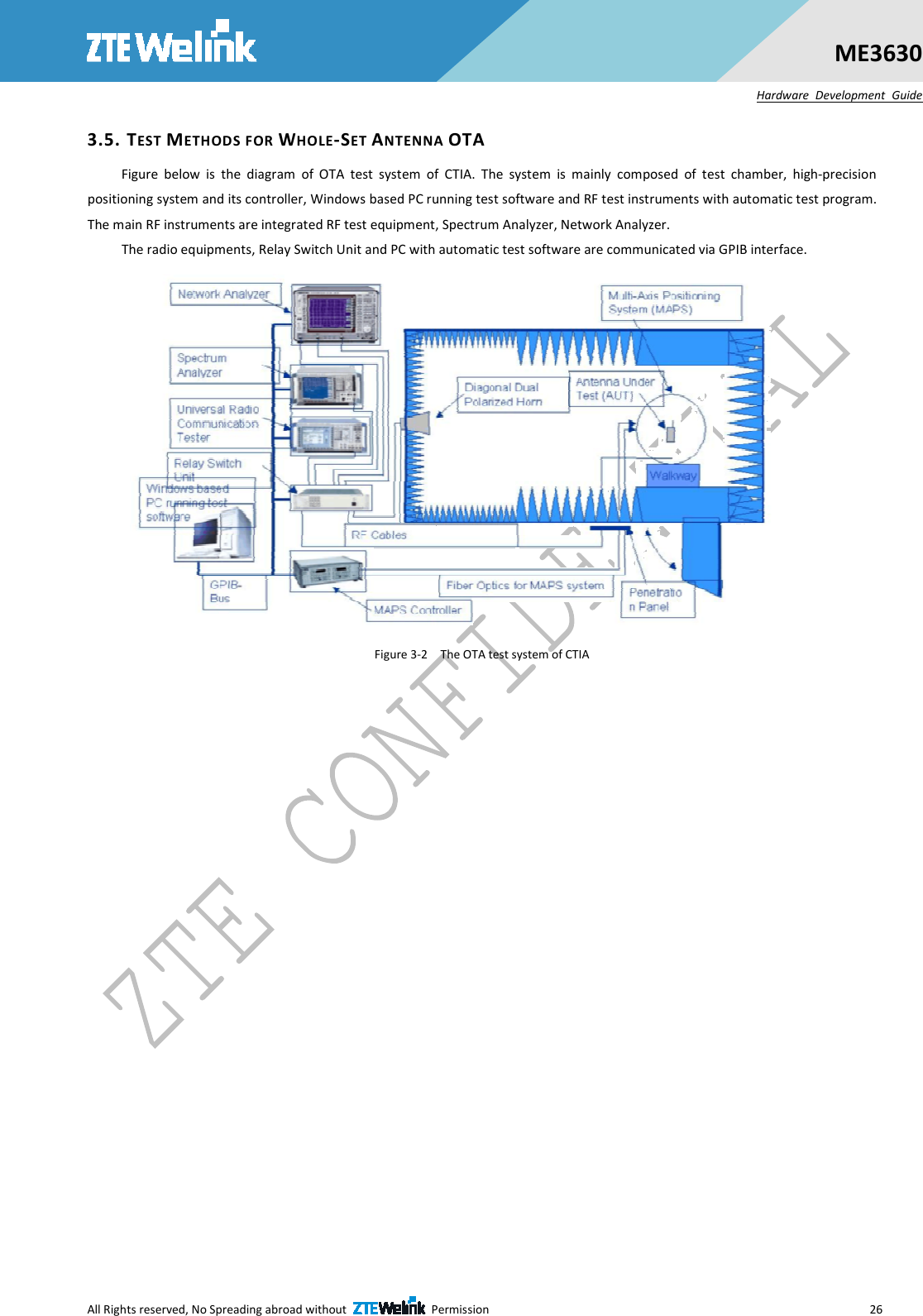
![All Rights reserved, No Spreading abroad without Permission 23 ME3630 Hardware Development Guide Table 2-16 Characteristic of the ADC Item Min Typ. Max Unit ADC1 voltage range 0.05 1.75 V ADC2 voltage range 0.05 1.75 V ADC resolution 15 Bits 2.11. WAKEUP_OUT SIGNAL The module provides an AP control interface for communicating with external Application Processor including WAKEUP_OUT. The following table shows the pin definition of AP control interface. Table 2-17 Pin Definition of WAKEUP_OUT Pin Name Pin NO. I/O Description Comment WAKEUP_OUT 71 DO Output wakeup signal 1.8V power domain When there is a SMS received by the module, it will output the level shown as the figure below through pin 71. Figure 2-17 The output signal of WAKEUP_OUT NOTE: WAKEUP_OUT is only supported SMS by the firmware version of ME3630 currently. 2.12. GPIO INTERFACE Module provides 8 GPIO pins. The direction and output voltage level of the GPIO can be set by AT command “AT+ZGPIO”. The input voltage level of the GPIO can also be read by AT command “AT+ZGPIO”. For more details of these AT commands, please refer to document [ME3630_AT_Commands_Manual_V1.0]. Table 2-18 Pin Definition of GPIO Pin Name Pin NO. I/O Description Comment GPIO1 7 IO General input/output 1.8V power domain GPIO2 8 IO General input/output 1.8V power domain GPIO3 12 IO General input/output 1.8V power domain GPIO4 13 IO General input/output 1.8V power domain GPIO5 27 IO General input/output 1.8V power domain GPIO6 28 IO General input/output 1.8V power domain GPIO7 29 IO General input/output 1.8V power domain GPIO8 30 IO General input/output 1.8V power domain GPIO9 64 IO General input/output 1.8V power domain GPIO10 65 IO General input/output 1.8V power domain GPIO11 75 IO General input/output 1.8V power domain GPIO12 76 IO General input/output 1.8V power domain GPIO13 77 IO General input/output 1.8V power domain](https://usermanual.wiki/ZTE/ME3630/User-Guide-3093421-Page-33.png)
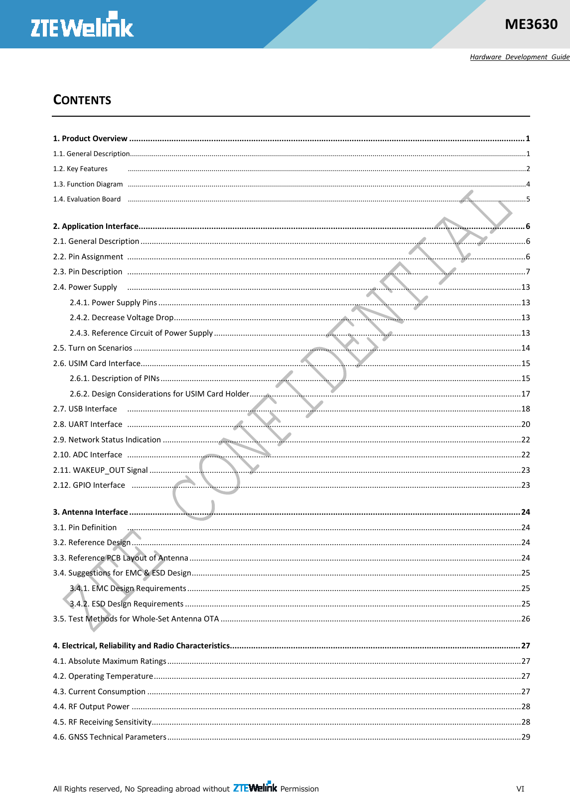
![All Rights reserved, No Spreading abroad without Permission 27 ME3630 Hardware Development Guide 4. ELECTRICAL, RELIABILITY AND RADIO CHARACTERISTICS 4.1. ABSOLUTE MAXIMUM RATINGS Absolute maximum ratings for power supply and voltage on digital and analog pins of module are listed in the following table: Table 4-1 Absolute Maximum Ratings Parameter Min Max Unit V_BAT -0.5 6.0 V Peak current of V_BAT 0 2 A Voltage at digital pin -0.3 2.1 V Voltage at ADC1 0.05 1.75 V Voltage at ADC2 0.05 1.75 V 4.2. OPERATING TEMPERATURE The operating temperature is listed in the following table. Table 4-2 Operating Temperature Parameter Min Typ. Max Unit Normal Temperature -30 25 75 ℃ Storage Temperature -40 85 ℃ NOTE: 1) When the module works within the temperature range, the deviations from the RF specification may occur. For example, the frequency error or the phase error would increase. 4.3. CURRENT CONSUMPTION The values of current consumption in different operating mode are shown below. Table 4-3 Averaged standby DC power consumption [1] Parameter Condition Typical Value Unit OFF state Power down 45 Sleep All system is halted 1.5 Table 4-4 Averaged standby DC power consumption [2] Parameter Condition Typical Value Unit Bandwidth 5MHz 10MHz 15MHz 20MHz LTE LTE FDD Band 1, Pout=23dBm 550 560 590 600 mA LTE FDD Band 3, Pout=23dBm 500 520 580 590 mA LTE TDD Band 38 ,Pout=23dBm 380 390 430 450 mA LTE TDD Band 39 ,Pout=23dBm 300 310 360 390 mA LTE TDD Band 40, Pout=23dBm 350 360 400 430 mA LTE TDD Band 41, Pout=23dBm 380 390 430 450 mA](https://usermanual.wiki/ZTE/ME3630/User-Guide-3093421-Page-37.png)
![All Rights reserved, No Spreading abroad without Permission 28 ME3630 Hardware Development Guide Table 4-5 Averaged standby DC power consumption [3] Parameter Condition Typical Value Unit WCDMA Band1 ,Pout=24dBm 550 mA TD-SCDMA Band34, Pout=24dBm 180 mA Band39, Pout=24dBm 180 mA CDMA BC0, Pout=23dBm 600 mA GSM Band3, Pout=30dBm 200 mA Band8, Pout=33dBm 300 mA 4.4. RF OUTPUT POWER The following table shows the RF output power of ME3630 module. Table 4-6 Conducted RF Output Power Frequency Max Min LTE FDD Band 1 23dBm ±2.7dB <-39dBm LTE FDD Band 3 23dBm ±2.7dB <-39dBm LTE TDD Band38 23dBm ±2.7dB <-39dBm LTETDD Band 39 23dBm ±2.7dB <-39dBm LTE TDD Band40 23dBm ±2.7dB <-39dBm LTE TDD Band 41 23dBm ±2.7dB <-39dBm WCDMA Band1 24+1/-3 dBm <-50dBm TD-SCDMA Band34 24+1/-3 dBm <-50dBm TD-SCDMA Band39 24+1/-3 dBm <-50dBm CDMA BC0 23~30 dBm <-50dBm GSM Band3 30dBm ±2dB <-50dBm GSM Band8 33dBm ±2dB <-50dBm 4.5. RF RECEIVING SENSITIVITY The following table shows the conducted RF receiving sensitivity of ME3630 module. Table 4-7 Conducted RF Receiving Sensitivity [1] Band 5 MHz(dBm) 10 MHz(dBm) 20 MHz(dBm) LTE FDD Band 1 -100 dBm -97 dBm -94 dBm LTE FDD Band 3 -97 dBm -94dBm -91dBm LTE TDD Band 38 -100 dBm -97 dBm -94 dBm LTE TDD Band 39 -100 dBm -97 dBm -94 dBm LTE TDD Band 40 -100 dBm -97 dBm -94 dBm LTE TDD Band 41 -100 dBm -97 dBm -94 dBm Table 4-8 Conducted RF Receiving Sensitivity [2] Band Sensitivity WCDMA Band1 -107 dBm TD-SCDMA BAND34 -108 dBm -108 dBm TD-SCDMA BAND39](https://usermanual.wiki/ZTE/ME3630/User-Guide-3093421-Page-38.png)