ZTE ME3631 LTE Module User Manual
ZTE Corporation LTE Module
UserManual.wiki
>
ZTE
>
ME3631 User Manual
User Manual
Navigation menu
Upload a User Manual
Namespaces
Wiki Guide
HTML
PDF
Info
Views
User Manual
Discussion / Help
Navigation
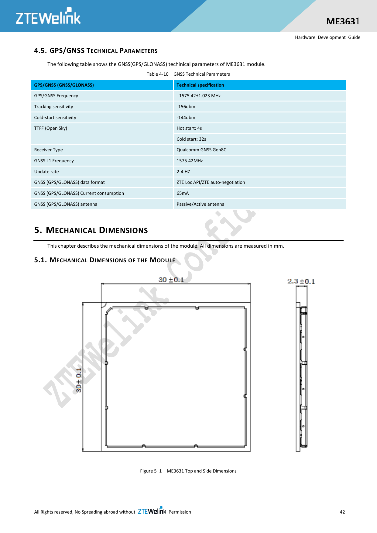
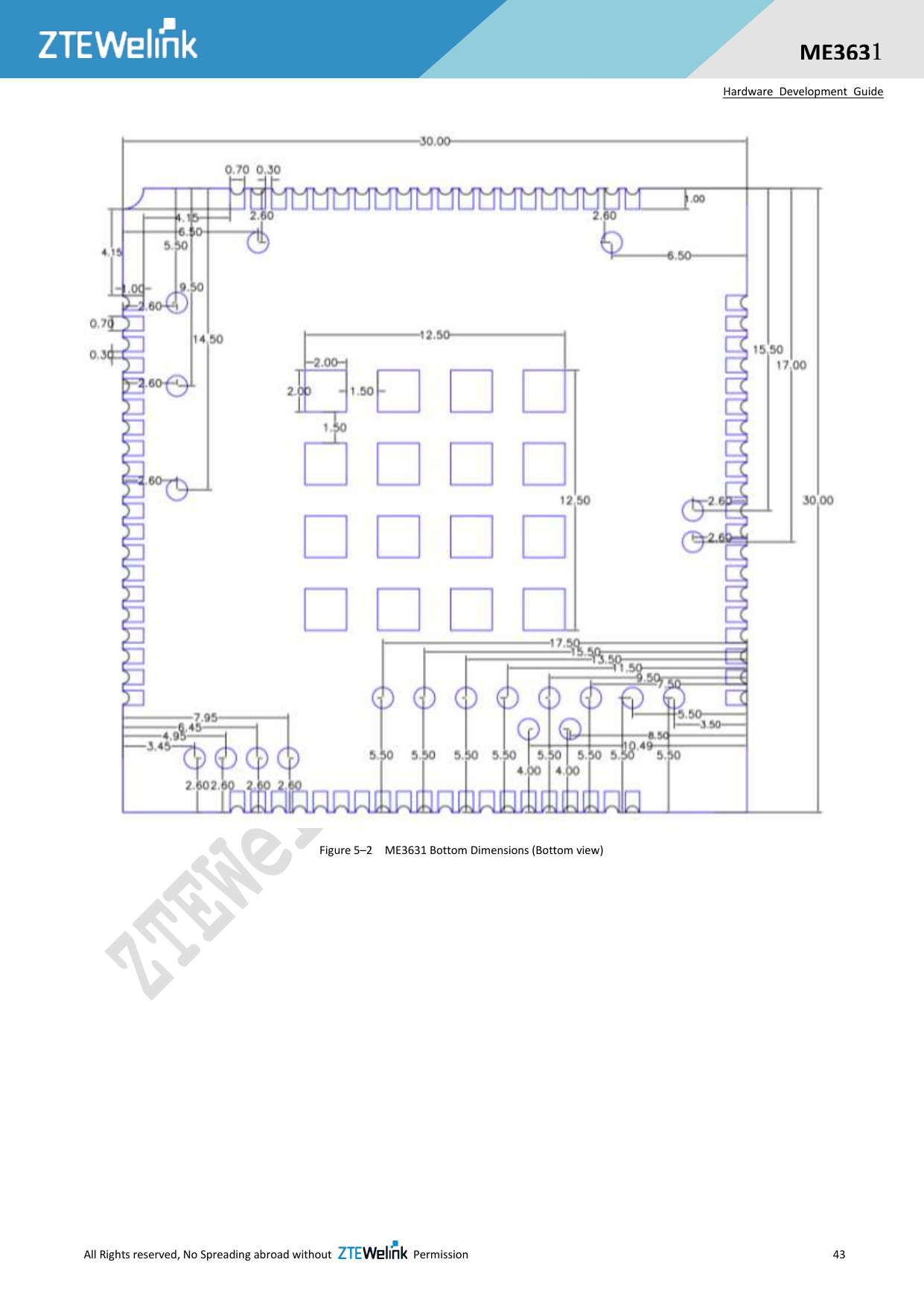
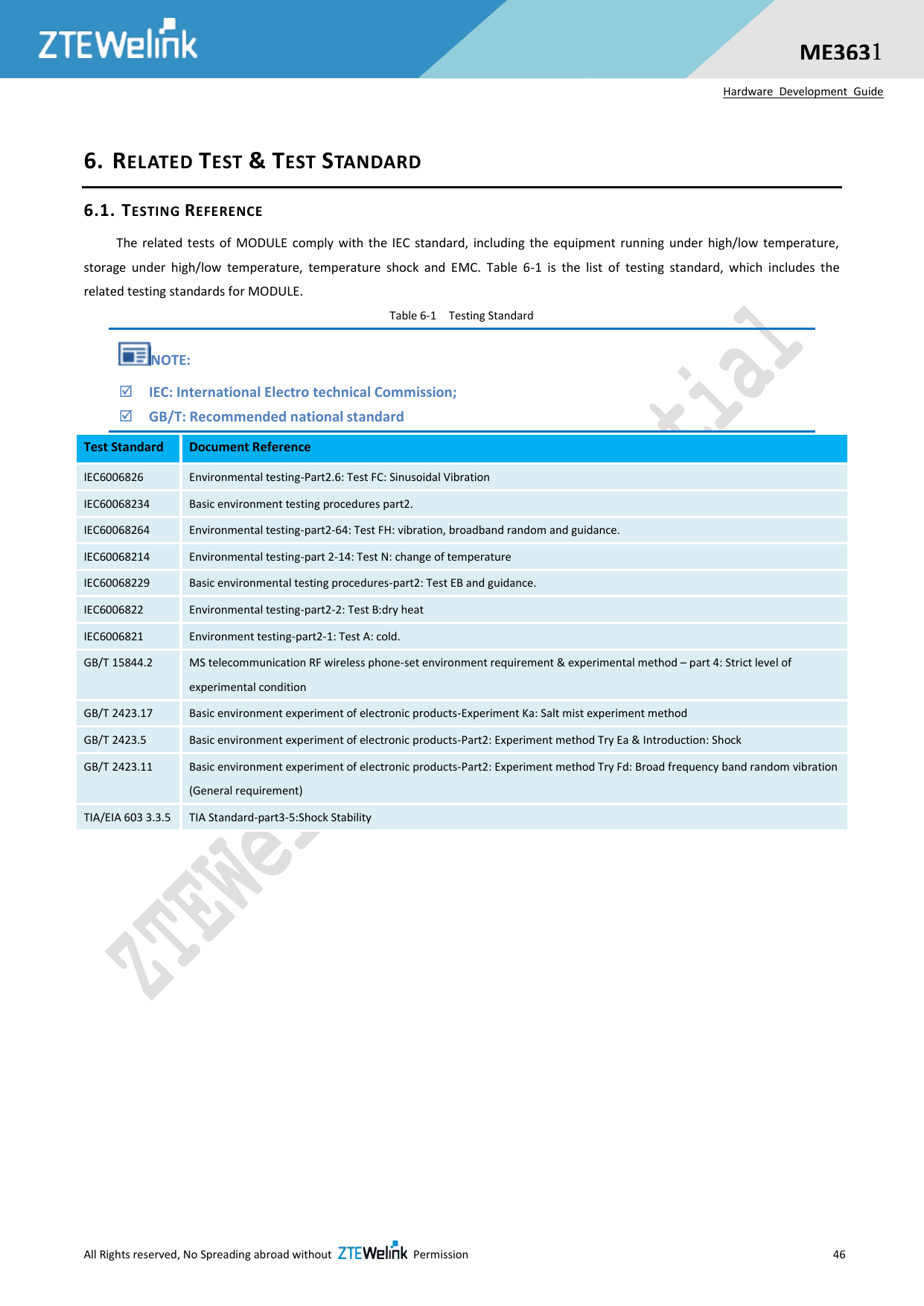
![All Rights reserved, No Spreading abroad without Permission VII ME3631 Hardware Development Guide TABLES Table 1-1 ME3631 Supported Band ................................................................................................ 11 Table 1-2 ME3631 Key Features .................................................................................................. 11 Table 2-1 IO Parameters Definition .............................................................................................. 15 Table 2-2 Logic levels Description ................................................................................................ 16 Table 2-3 Pin Description ............................................................................................................. 16 Table 2-4 Power Supply ............................................................................................................... 21 Table 2-5 POWER_ON/OFF Pin Description ............................................................................... 23 Table 2-6 Power-on Time ............................................................................................................. 23 Table 2-7 Pin Definition of the USIM Interface .............................................................................. 25 Table 2-8 Pin Description of Molex USIM Card Holder ................................................................. 28 Table 2-9 Pin Description of Amphenol USIM Card Holder........................................................... 29 Table 2-10 USB Pin Description ................................................................................................... 30 Table 2-11 Pin Definition of the Main UART Interface .................................................................. 31 Table 2-12 Pin Definition of the Debug UART Interface ................................................................ 31 Table 2-13 Pin Definition of Network Indicator .............................................................................. 33 Table 2-14 Working State of the Network Indicator ...................................................................... 33 Table 2-15 Pin Definition of the ADC ............................................................................................ 33 Table 2-16 Characteristic of the ADC ........................................................................................... 33 Table 2-17 Pin Definition of WAKEUP_IN .................................................................................... 34 Table 2-18 Pin Definition of WAKEUP_OUT ................................................................................ 35 Table 2-19 Pin Definition of GPIO ................................................................................................ 36 Table 3-1 Pin Definition of GPIO .................................................................................................. 37 Table 4-1 Absolute Maximum Ratings .......................................................................................... 40 Table 4-2 Operating Temperature ................................................................................................ 40 Table 4-3 ESD characteristic ........................................................................................................ 40 Table 4-4 Averaged standby DC power consumption [1] .............................................................. 40 Table 4-5 Averaged standby DC power consumption [2] .............................................................. 40 Table 4-6 Averaged standby DC power consumption [3] .............................................................. 41 Table 4-7 Conducted RF Output Power........................................................................................ 41](https://usermanual.wiki/ZTE/ME3631/User-Guide-3438954-Page-8.png)
![All Rights reserved, No Spreading abroad without Permission VIII ME3631 Hardware Development Guide Table 4-8 Conducted RF Receiving Sensitivity Typical Value [1] .................................................. 41 Table 4-9 Conducted RF Receiving Sensitivity Typical Value [2] .................................................. 41 Table 4-10 GNSS Technical Parameters ...................................................................................... 42 Table 6-1 Testing Standard .......................................................................................................... 46 Table 6-2 Testing Environment .................................................................................................... 47 Table 6-3 Testing Instrument & Device......................................................................................... 47 Table 6-4 Reliability Features ....................................................................................................... 48 Table 7-1 Baking parameters ....................................................................................................... 49 Table 7-2 LCC module PAD’s steel mesh opening ................................................................................ 49](https://usermanual.wiki/ZTE/ME3631/User-Guide-3438954-Page-9.png)
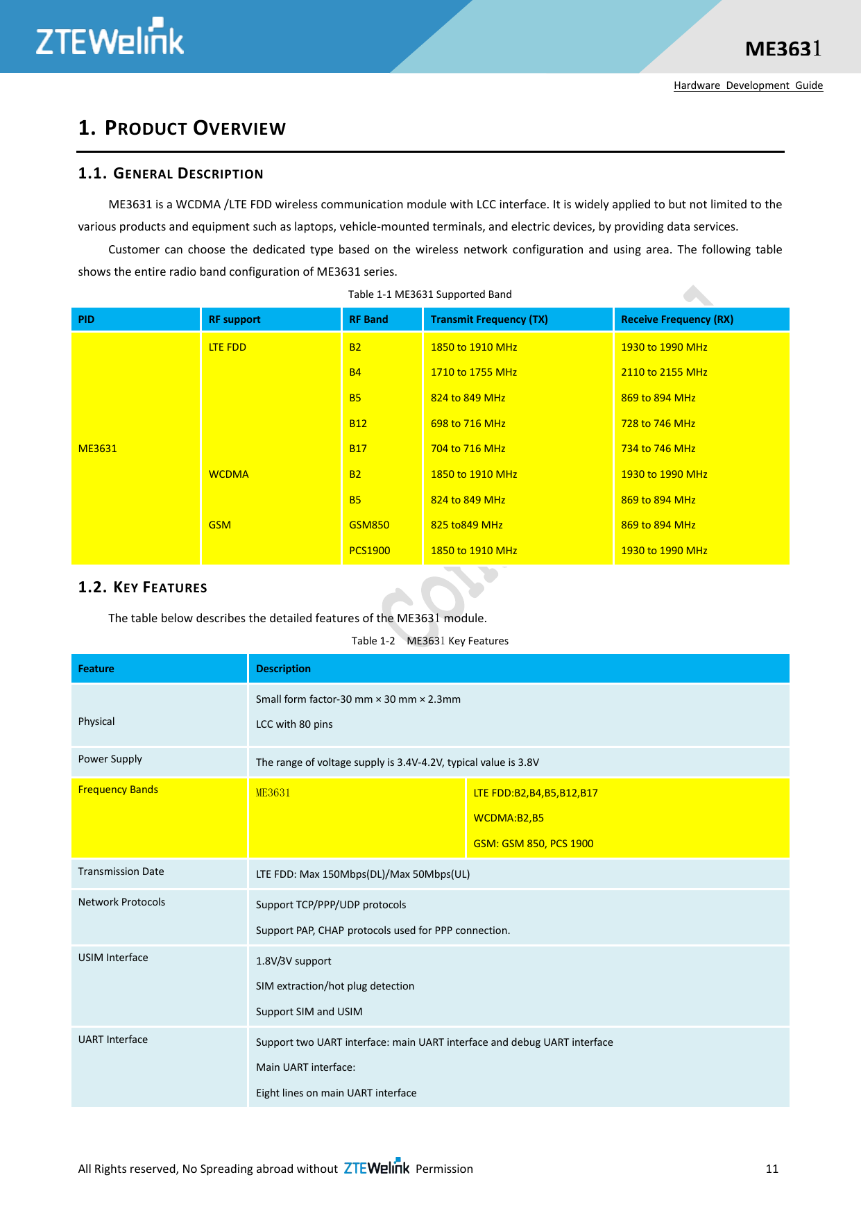
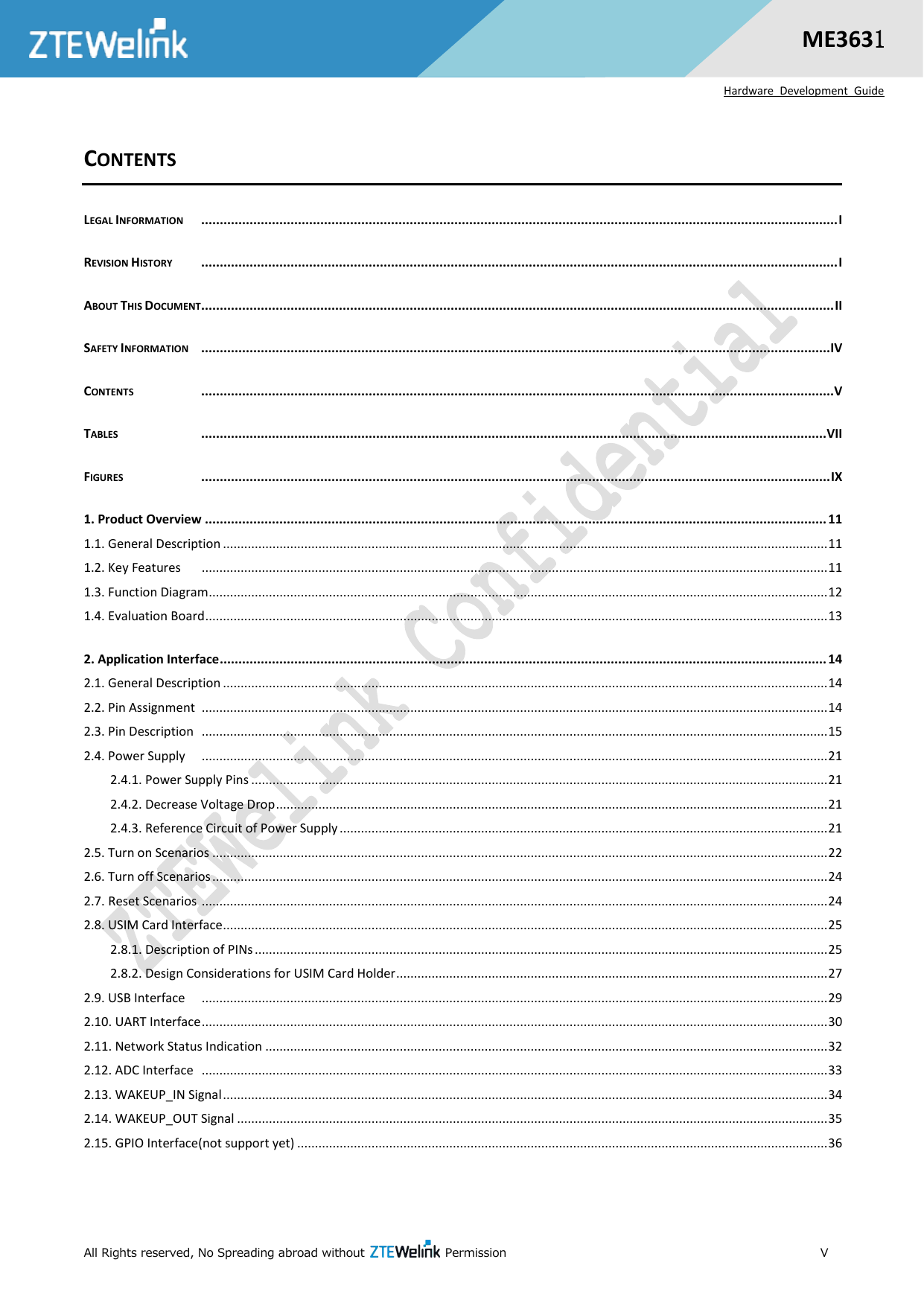
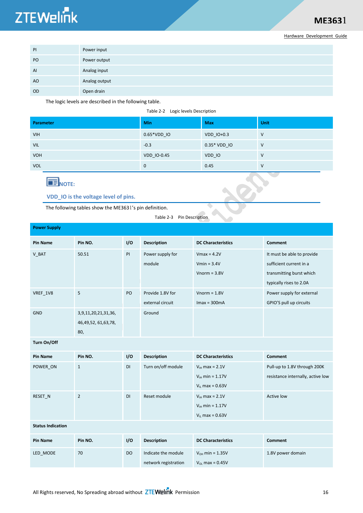
![All Rights reserved, No Spreading abroad without Permission 13 ME3631 Hardware Development Guide --Status interface (LED) BasebandUSBUSIMUARTI2CSDIOSPILEDADCGPIOFLASH&LPDDR2DataControlControlRx&TxRF TransceiverRF PA DuplexerDuplexerTxRxMAIN_ANT80PIN LCC Connector InterfaceRx GNSSRx DIV_ANT Figure 1–1 System Connection Structure 1.4. EVALUATION BOARD In order to help you to develop applications with ME3631, ZTEWelink supplies an evaluation board (G2000/GE2015), RS-232 to USB cable, USB data cable, power adapter, antenna and other peripherals to control or test the module. For details, please refer to the related document [ZTEWelink G2000 Dev Board User Guide] or [ZTEWelink GE2015 Dev Board User Guide].](https://usermanual.wiki/ZTE/ME3631/User-Guide-3438954-Page-14.png)
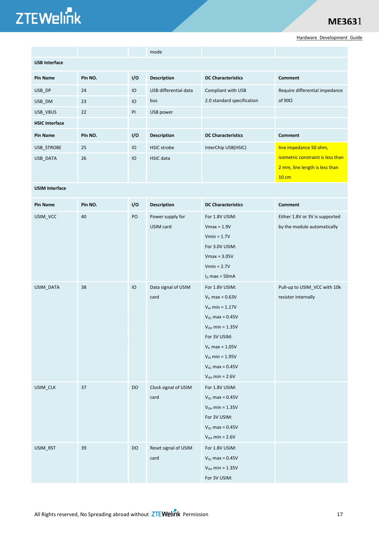
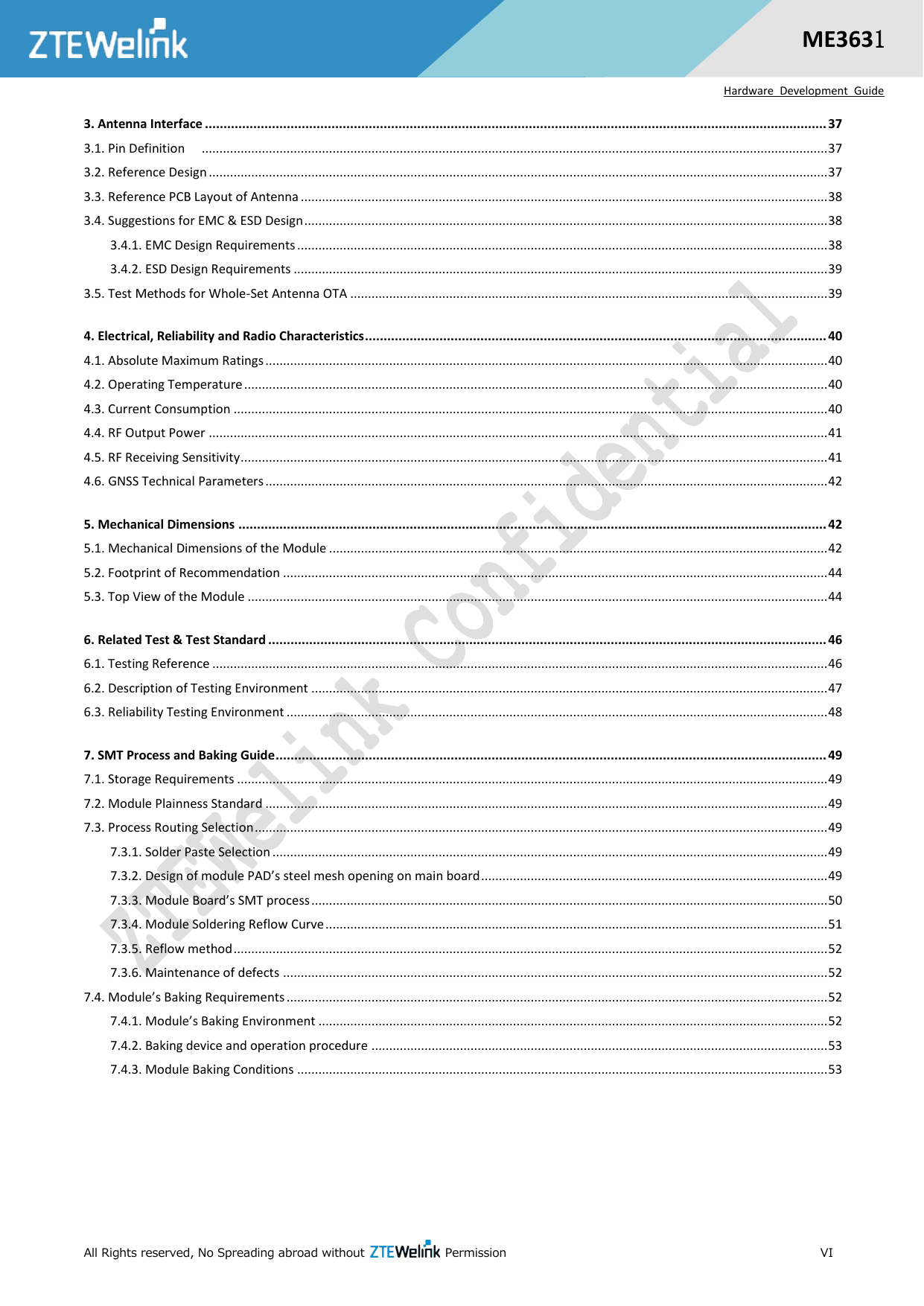
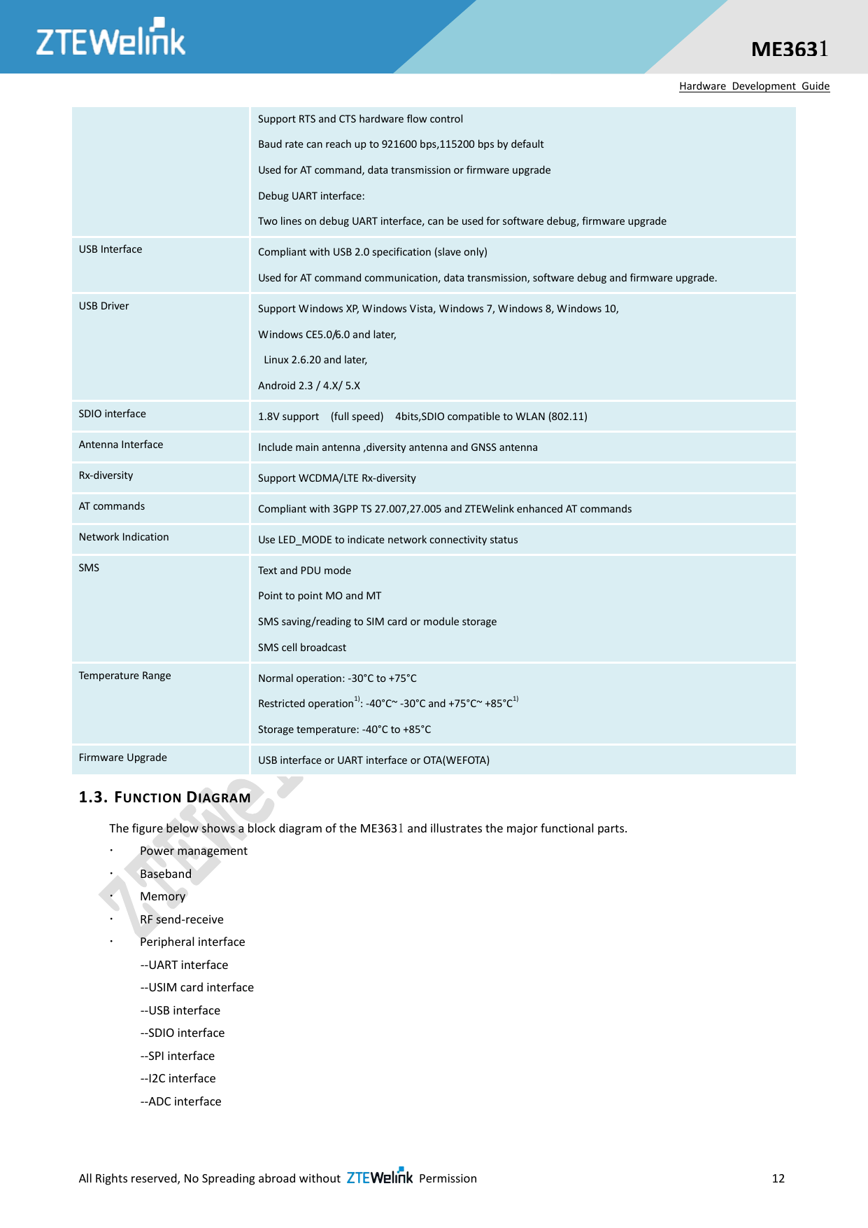
![All Rights reserved, No Spreading abroad without Permission 19 ME3631 Hardware Development Guide UART_DEBUG_RXD 67 DI Receive data VIL min = -0.3V VIL max = 0.63V VIH min = 1.17V VIH max = 2.1V 1.8V power domain RF Interface Pin Name Pin NO. I/O Description DC Characteristics Comment MAIN_ANT 62 IO Main antenna 50Ω impedance DIV_ANT 79 AI Diversity antenna 50Ω impedance GNSS_ANT 10 IO GNSS antenna 50Ω impedance I2C Interface Pin Name Pin NO. I/O Description DC Characteristics Comment I2C_SCL 73 DO I2C serial clock VOL max = 0.45V VOH min = 1.35V Pull-up to 1.8V through external 2.2K resistance, active low [can use the power of pin 5] I2C_SDA 74 IO I2C serial data VOL max = 0.45V VOH min = 1.35V VIL min = -0.3V VIL max = 0.63V VIH min = 1.17V VIH max = 2.1V Pull-up to 1.8V through external 2.2K resistance, active low [can use the power of pin 5] SDIO Interface Pin Name Pin NO. I/O Description DC Characteristics Comment SDIO_CMD 14 IO Secure digital CMD VOL max = 0.45V VOH min = 1.35V VIL min = -0.3V VIL max = 0.63V VIH min = 1.17V VIH max = 2.1V Pull-up to 1.8V through external 10K resistance, active low [can use the power of pin 5] SDIO_CLK 19 DO Secure digital CLK VOL max = 0.45V VOH min = 1.35V 1.8V power domain SDIO_D0 15 IO Secure digital IO data bit 0 VOL max = 0.45V VOH min = 1.35V VIL min = -0.3V VIL max = 0.63V VIH min = 1.17V VIH max = 2.1V 1.8V power domain SDIO_D1 16 IO Secure digital IO data bit 1 VOL max = 0.45V VOH min = 1.35V VIL min = -0.3V 1.8V power domain](https://usermanual.wiki/ZTE/ME3631/User-Guide-3438954-Page-20.png)
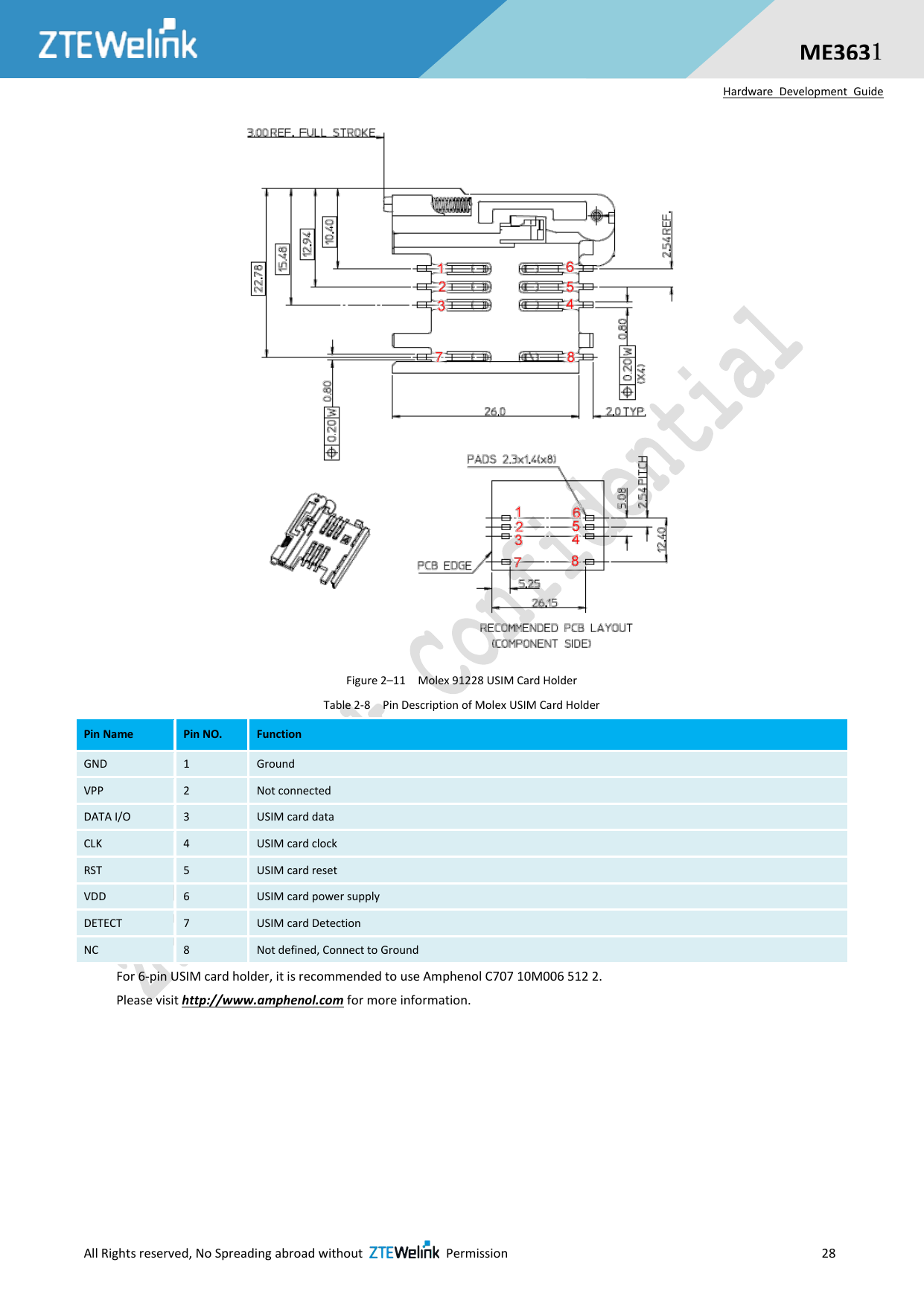
![All Rights reserved, No Spreading abroad without Permission 26 ME3631 Hardware Development Guide USIM_RST 39 DO Reset signal of USIM card USIM_DETECT 41 DI USIM card hot swap detection pin. 1.8V power domain. The signal is internally pulled up. Keep USIM_DETECT not connected, if it is not used. When USIM detect function is enable (send AT command AT+ZSDT=1), and if it is Low, USIM is present; if it is High, USIM is absent. GND 36 Ground The following figure shows the reference design of the 8-pin USIM card. Figure 2–9 Reference Circuit of the 8 Pin USIM Card NOTE: R10~R12 and D5 are applied to suppress the EMI spurious transmission and enhance the ESD protection.Should be closed to J3. USIM_DETECT is used to detect USIM card, which will be low when the USIM card is inserted. The value of C29 shoule be less than 1uF ME3631 supports USIM card hot-plugging via the USIM_ DETECT pin. For details, refer to document [AT Command Reference Guide of Module Product ME3631_V1.0]. If you do not need the USIM card detect function, keep USIM_ DETECT unconnected. The reference circuit for using a 6-pin USIM card socket is illustrated as the following figure. Figure 2–10 Reference Circuit of the 6 Pin USIM Card](https://usermanual.wiki/ZTE/ME3631/User-Guide-3438954-Page-27.png)
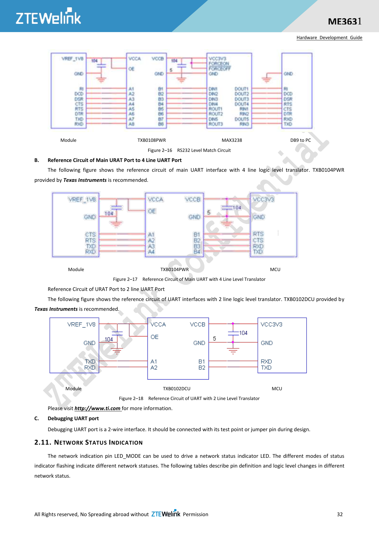
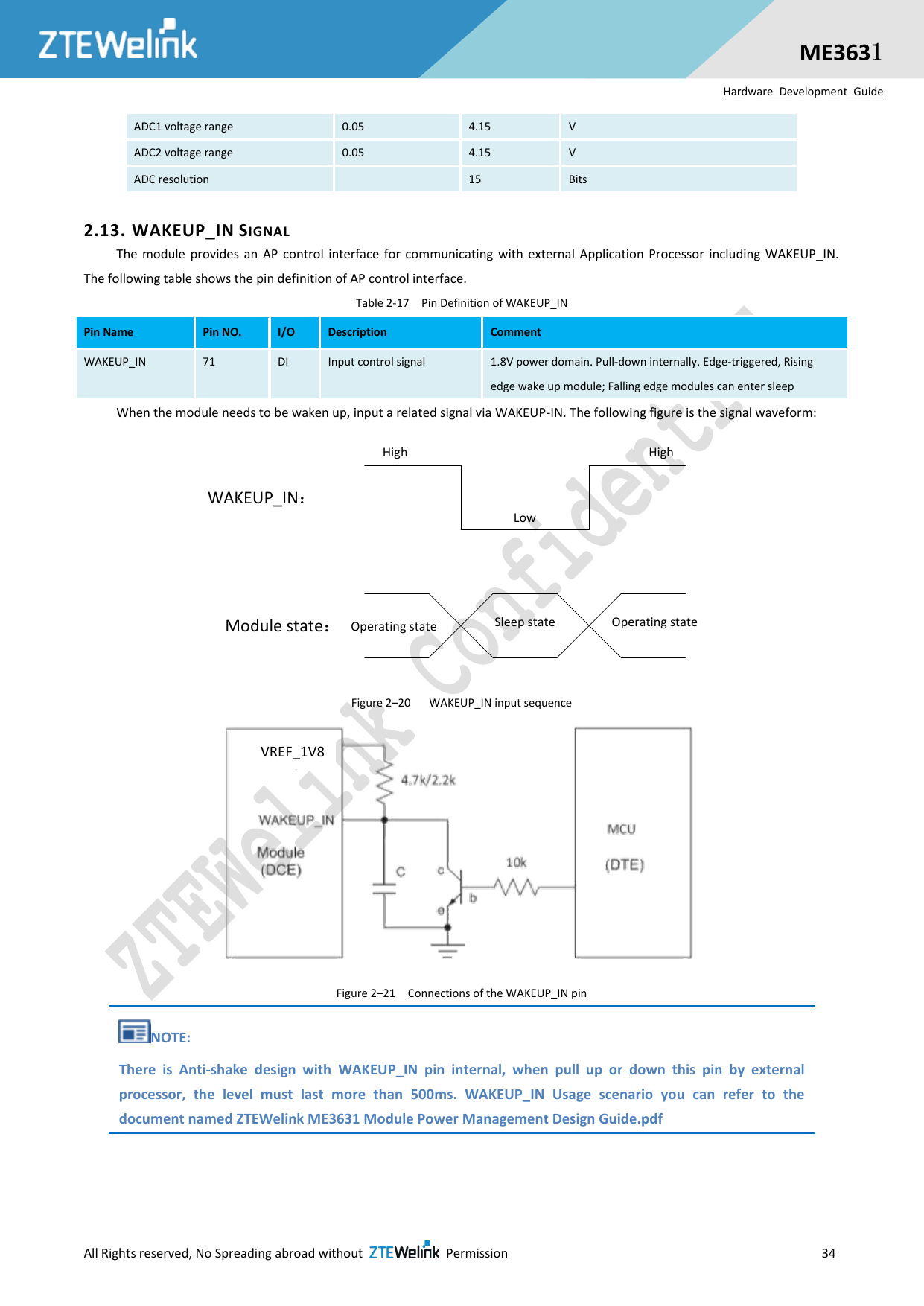
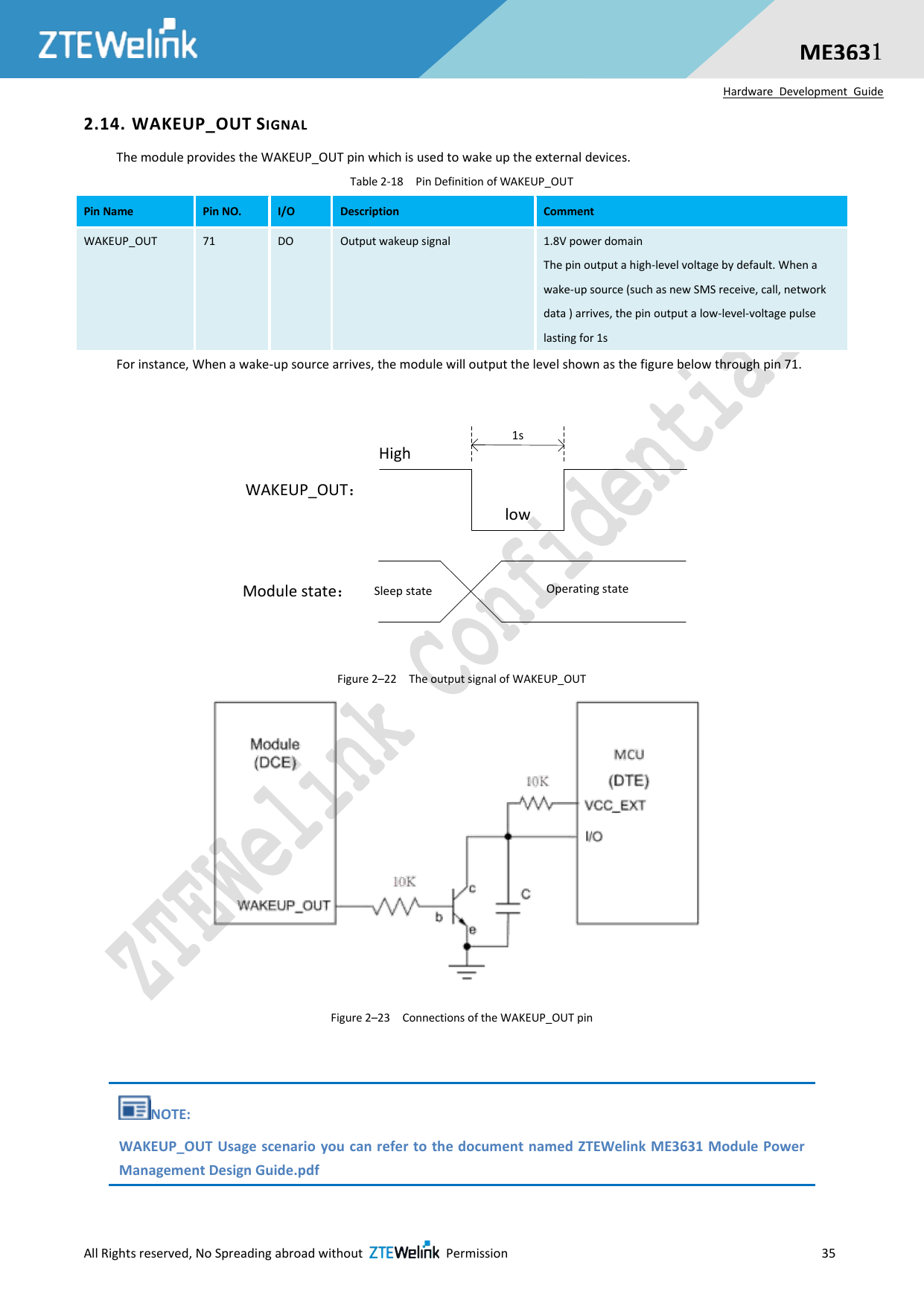
![All Rights reserved, No Spreading abroad without Permission 33 ME3631 Hardware Development Guide Table 2-13 Pin Definition of Network Indicator Pin Name Pin NO. I/O Description Comment LED_MODE 70 DO Indicate the module network registration mode 1.8V power domain Table 2-14 Working State of the Network Indicator LED Status Module status High level, LED on Module register to network success Low level, LED off Module not register to network(module is in flight mode or power off) Low level 1s(LED off), High level 1s(LED on) PDP activated, and get the IP address or Socket established Figure below is the reference circuit design diagram. NOTE: The resistors R1, R2 and R3 in Figures below are only the recommended value and they need to adjust according to the actual situation. Figure 2–19 Reference Circuit of the Network Indicator 2.12. ADC INTERFACE The module provides two ADCs to digitize the analog signal to 10-bit digital data such as battery voltage, temperature and so on. Using AT command “AT+ZADC1?” can read the voltage value on ADC1 pin. Using AT command “AT+ZADC2?” can read the voltage value on ADC2 pin. The read value is expressed in mV. For more details of these AT commands, please refer to document [AT Command Reference Guide of Module Product ME3631_V1.0]. In order to improve the accuracy of ADC, the trace of ADC should be surrounded by ground. Table 2-15 Pin Definition of the ADC Pin Name Pin NO. Description ADC1 48 General purpose analog to digital converter. ADC2 47 General purpose analog to digital converter. The following table describes the characteristic of the ADC function. Table 2-16 Characteristic of the ADC Item Min Max Unit](https://usermanual.wiki/ZTE/ME3631/User-Guide-3438954-Page-34.png)
![All Rights reserved, No Spreading abroad without Permission 36 ME3631 Hardware Development Guide 2.15. GPIO INTERFACE(NOT SUPPORT YET) Module provides 9 GPIO pins. The direction and output voltage level of the GPIO can be set by AT command “AT+ZGPIO”. The input voltage level of the GPIO can also be read by AT command “AT+ZGPIO”. For more details of these AT commands, please refer to document [AT Command Reference Guide of Module Product ME3631_V1.0]. Table 2-19 Pin Definition of GPIO Pin Name Pin NO. I/O Description Comment GPIO1 7 IO General input/output 1.8V power domain GPIO2 8 IO General input/output 1.8V power domain GPIO3 12 IO General input/output 1.8V power domain GPIO4 13 IO General input/output 1.8V power domain GPIO5 27 IO General input/output 1.8V power domain GPIO6 28 IO General input/output 1.8V power domain GPIO7 29 IO General input/output 1.8V power domain GPIO8 30 IO General input/output 1.8V power domain GPIO9 65 IO General input/output 1.8V power domain](https://usermanual.wiki/ZTE/ME3631/User-Guide-3438954-Page-37.png)
![All Rights reserved, No Spreading abroad without Permission 40 ME3631 Hardware Development Guide 4. ELECTRICAL, RELIABILITY AND RADIO CHARACTERISTICS 4.1. ABSOLUTE MAXIMUM RATINGS Absolute maximum ratings for power supply and voltage on digital and analog pins of module are listed in the following table: Table 4-1 Absolute Maximum Ratings Parameter Min Max Unit V_BAT 3.4 4.2 V Peak current of V_BAT 0 2 A Voltage at digital pin -0.3 2.1 V Voltage at ADC1 0.05 4.15 V Voltage at ADC2 0.05 4.15 V 4.2. OPERATING TEMPERATURE The operating temperature is listed in the following table. Table 4-2 Operating Temperature Parameter Min Typ. Max Unit Normal Temperature -30 25 75 ℃ Storage Temperature -40 85 ℃ Extreme Operating Temperature -40°C~ -30°C / +75°C~ +85°C ℃ 4.3. ELECTROSTATIC DISCHARGE The module is not protected against electrostatics discharge (ESD) in general. Consequently, it is subject to ESD handling precautions that typically apply to ESD sensitive components. Proper ESD handling and packaging procedures must be applied throughout the processing, handling and operation of any application that incorporates the module. The following table shows the module electrostatics discharge characteristics. Table 4-3 ESD characteristic Tested Points Contact discharge Air Discharge Unit V_BAT ± 5 ± 10 kV All antenna interfaces ±4 ± 8 kV Other interfaces ± 0.5 ± 1 kV 4.4. ME3631-U TEST 4.4.1. CURRENT CONSUMPTION The values of current consumption in different operating mode are shown below. Table 4-4 Averaged standby DC power consumption [1] Parameter Condition Typical Value Unit OFF state Power down 45 uA Base Current Flight Mode[Sleep] 0.9 mA Table 4-5 Averaged standby DC power consumption [2] Parameter Condition Typical Value Unit](https://usermanual.wiki/ZTE/ME3631/User-Guide-3438954-Page-41.png)
![All Rights reserved, No Spreading abroad without Permission 41 ME3631 Hardware Development Guide Bandwidth 5MHz 10MHz 15MHz 20MHz LTE LTE FDD Band 2, Pout=23dBm 575 575 620 630 mA LTE FDD Band 4, Pout=23dBm 515 530 550 600 mA LTE FDD Band 5 ,Pout=23dBm 610 610 mA LTE FDD Band 12,Pout=23dBm 620 630 mA LTE FDD Band 17, Pout=23dBm 550 600 mA Table 4-6 Averaged standby DC power consumption [3] Parameter Condition Typical Value Unit WCDMA Band2, Pout=24dBm 532 mA Band5, Pout=24dBm 526 mA GSM GSM850, Pout=33dBm 280 mA PCS1900, Pout=29dBm 260 mA 4.4.2. RF OUTPUT POWER The following table shows the RF output power of ME3631 module. Table 4-7 Conducted RF Output Power Frequency Max Min LTE FDD Band 2 23±2.7dBm -39dBm LTE FDD Band 4 23 ±2.7dBm -39dBm LTE FDD Band 5 23 ±2.7dBm -39dBm LTE FDD Band 12 23 ±2.7dBm -39dBm LTE FDD Band 17 23 ±2.7dBm -39dBm WCDMA Band 2 24+1/-3 dBm -50dBm WCDMA Band 5 24+1/-3 dBm -50dBm GSM850 33+-2 5±5dBm PCS1900 30 ±2dBm 0 ±5dBm 4.4.3. RF RECEIVING SENSITIVITY The following table shows the conducted RF receiving sensitivity typical value of ME3631 module. Table 4-8 Conducted RF Receiving Sensitivity Typical Value [1] Band 5 MHz(dBm) 10 MHz(dBm) 20 MHz(dBm) LTE FDD Band 2 -98 dBm -95 dBm -92 dBm LTE FDD Band 4 -100 dBm -97 dBm -94 dBm LTE FDD Band 5 -98 dBm -95 dBm LTE FDD Band 12 -97 dBm -94 dBm LTE FDD Band 17 -97 dBm -94 dBm Table 4-9 Conducted RF Receiving Sensitivity Typical Value [2] Band Sensitivity WCDMA Band 2 -104.7 dBm WCDMA Band 5 -104.7 dBm GSM850 -107 dBm PCS1900 -107 dBm](https://usermanual.wiki/ZTE/ME3631/User-Guide-3438954-Page-42.png)