User Manual

HARDWARE DEVELOPMENT GUIDE
Version: V1.1
Date: 2017-02-23
LTE Module Series
ME3631
Website: www.ztewelink.com
E-mail: ztewelink@zte.com.cn
All Rights reserved, No Spreading abroad without Permission I
ME3631
Hardware Development Guide
LEGAL INFORMATION
By receiving the document from Shenzhen ZTEWelink Technology Co., Ltd (shortly referred to as ZTEWelink), you are deemed
to have agreed to the following terms. If you don’t agree to the following terms, please stop using the document.
Copyright © 2017 Shenzhen ZTEWelink Technology Co., Ltd. All rights reserved. The document contains ZTEWelink’s
proprietary information. Without the prior written permission of ZTEWelink, no entity or individual is allowed to reproduce, transfer,
distribute, use and disclose this document or any image, table, data or other information contained in this document.
ZTEWelink is a holding subsidiary of ZTE Corporation, dedicate to cellular M2M communication modules and M2M solutions.
is the registered trademark of ZTE Corporation and ZTEWelink is granted to use ZTE Corporation’s registered trademarks.
The name and logo of ZTEWelink are ZTEWElink’s trademark or registered trademarks. The other products or company names
mentioned in this document are the trademark or registered trademark of their respective owner. Without the prior written
permission of ZTEWelink or the third-party oblige, no entity or individual is allowed to use any company name, trademark, logo, label
or other information contained in this document.
The product meets the design requirements of environmental protection and personal security. The storage, use or disposal of
products should abide by the product manual, relevant contract or the laws and regulations of relevant country.
ZTEWelink reserves the right to make modifications on the product described in this document without prior notice, and keeps
the right to revise or retrieve the document any time.
If you have any question about the manual, please consult the company or its distributors promptly.
Copyright © ZTEWeLink Technology Co., LTD, All rights reserved.
REVISION HISTORY
Version
Date
Description
1.0
2017-01-18
1st released version
All Rights reserved, No Spreading abroad without Permission II
ME3631
Hardware Development Guide
ABOUT THIS DOCUMENT
A. Application Range
This document is the Product Technical Specification for the ME3631 GSM/WCDMA/LTE-FDD module. It defines the high level
product features and illustrates the interface for these features. This document is intended to cover the hardware aspects of the
product, including electrical and mechanical.
B. Reading Note
The symbols below are the reading notes you should pay attention on:
: WARNING or ATTENTION : NOTE or REMARK
C. Purpose
This document provides the hardware solutions and development fundamentals for a product with the module. By reading this
document, the user can have an overall knowledge of the module and a clear understanding of the technical parameters. With this
document, the user can successfully fulfill the application and development of wireless Internet product or equipment.
Besides the product features and technical parameters, this document also provides the product reliability tests and related
testing standards, RF performance indexes and a guide on the design of user circuits, to provide the user with a complete design
reference.
NOTE:
To ensure the module manufacturing and welding quality, do as the chapter 7 of Manufacturing Guide in
this document. The force on the squeegee should be adjusted so as to produce a clean stencil surface on a
single pass and ensure the module soldering quality.
D. Abbreviations
Table below is a list of abbreviations involved in this document, as well as the English full names.
Abbreviations
Full Name
3GPP
Third Generation Partnership Project
AP
Another name of DTE
CHAP
Challenge Handshake Authentication Protocol
CE
European Conformity
CMOS
Complementary Metal Oxide Semiconductor
DCE
Data Communication Equipment
DL
Downlink
DTE
Data Terminal Equipment
EIA
Electronic Industries Association
EMC
Electromagnetic Compatibility
ESD
Electro-Static discharge
ESR
Equivalent Series Resistance
FDD
Frequency Division Duplex
GPIO
General-purpose I/O
LCC
Leadless Chip Carrier
All Rights reserved, No Spreading abroad without Permission III
ME3631
Hardware Development Guide
LDO
Low-Dropout
LED
Light Emitting Diode
LTE
Long Term Evolution
ME
Mobile Equipment
MO
Mobile Origination Call
MT
Mobile Termination Call
MSB
Most Significant Bit
PC
Personal Computer
PCB
Printed Circuit Board
PDA
Personal Digital Assistant
PDU
Protocol Data Unit
PAP
Password Authentication Protocol
PPP
Point to Point Protocol
RTC
Real Time Clock
SMS
Short Messaging Service
SMT
Surface Mount Technology
SPI
Serial Peripheral Interface
TBD
To Be Determined
TCP
Transmission Control Protocol
TIS
Total Isotropic Sensitivity
TRP
Total Radiated Power
TVS
Transient Voltage Suppressor
UART
Universal Asynchronous Receiver-Transmitter
UDP
User Datagram Protocol
UL
Up Link
USB
Universal Serial Bus
USIM
Universal Subscriber Identity Module
URC
Unsolicited result code
VIH
Logic High level of input voltage
VIL
Logic Low level of input voltage
VOH
Logic High level of output voltage
VOL
Logic Low level of output voltage
All Rights reserved, No Spreading abroad without Permission IV
ME3631
Hardware Development Guide
SAFETY INFORMATION
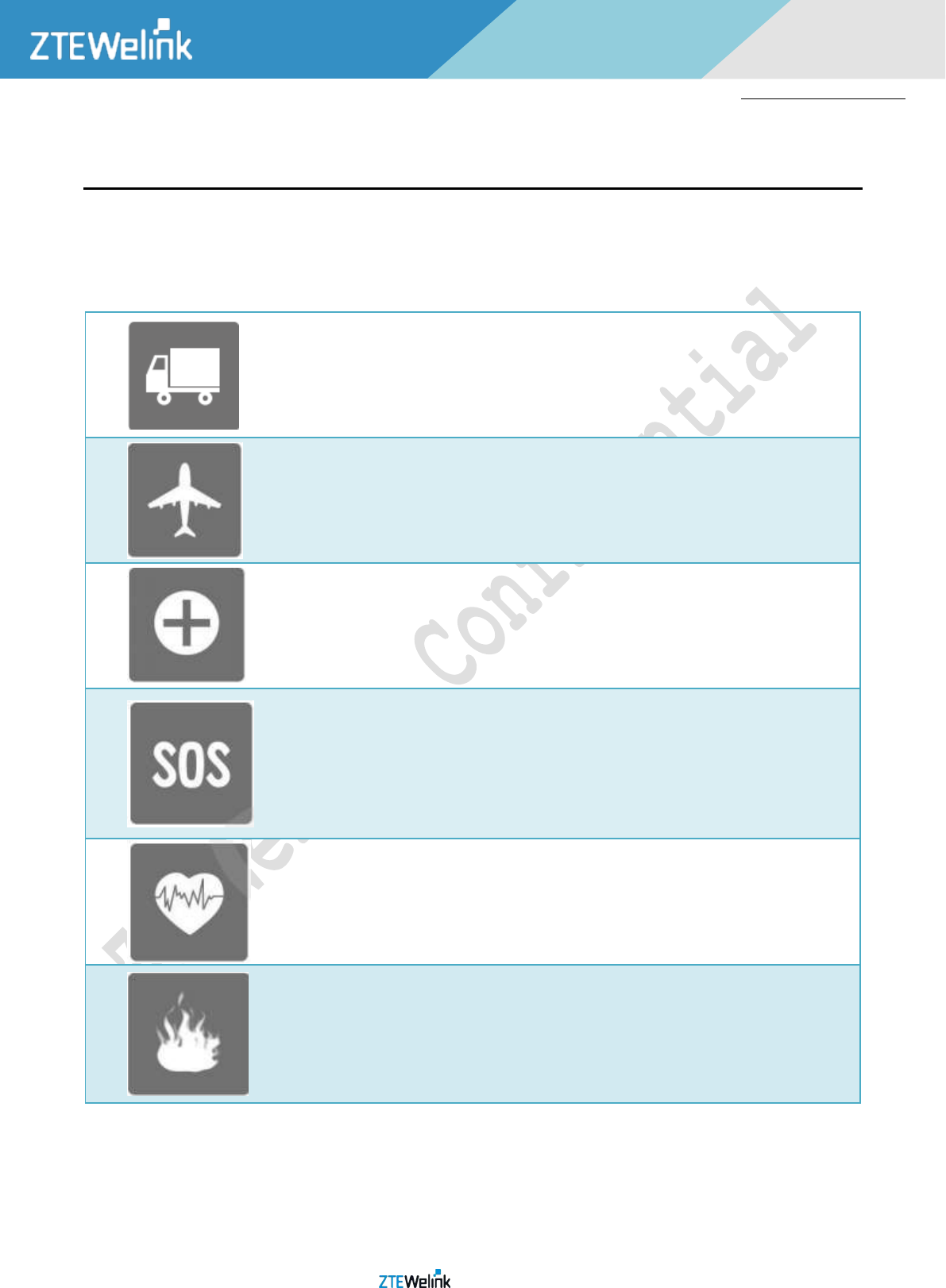
The following safety precautions must be observed during all phases of the operation, such as usage, service or repair of any
cellular terminal or mobile incorporating ME3610 module. Manufacturers of the cellular terminal should send the following safety
information to users and operating personnel and to incorporate these guidelines into all manuals supplied with the product. If not
so, ZTEWelink does not take on any liability for customer failure to comply with these precautions.
Full attention must be given to driving at all times in order to reduce the risk of an accident. Using a
mobile while driving (even with a hands free kit) cause distraction and can lead to an accident. You must
comply with laws and regulations restricting the use of wireless devices while driving.
Switch off the cellular terminal or mobile before boarding an aircraft. Make sure it switched off. The
operation of wireless appliances in an aircraft is forbidden to prevent interference with communication
systems. Consult the airline staff about the use of wireless devices on boarding the aircraft, if your device
offers a Airplane Mode which must be enabled prior to boarding an aircraft.
Switch off your wireless device when in hospitals or clinics or other health care facilities. These
requests are designed to prevent possible interference with sensitive medical equipment.
GSM cellular terminals or mobiles operate over radio frequency signal and cellular network and
cannot be guaranteed to connect in all conditions, for example no mobile fee or an invalid SIM card. While
you are in this condition and need emergent help, please remember using emergency call. In order to make
or receive call, the cellular terminal or mobile must be switched on and in a service area with adequate
cellular signal strength.
Your cellular terminal or mobile contains a transmitter and receiver. When it is on, it receives and
transmits radio frequency energy. RF interference can occur if it is used close to TV set, radio, computer or
other electric equipment.
In locations with potentially explosive atmospheres, obey all posted signs to turn off wireless devices
such as your phone or other cellular terminals. Areas with potentially explosive atmospheres including
fuelling areas, below decks on boats, fuel or chemical transfer or storage facilities, areas where the air
contains chemicals or particles such as grain, dust or metal powders.

All Rights reserved, No Spreading abroad without Permission V
ME3631
Hardware Development Guide
CONTENTS
LEGAL INFORMATION ........................................................................................................................................................................... I
REVISION HISTORY ........................................................................................................................................................................... I
ABOUT THIS DOCUMENT.......................................................................................................................................................................... II
SAFETY INFORMATION ......................................................................................................................................................................... IV
CONTENTS .......................................................................................................................................................................... V
TABLES ........................................................................................................................................................................ VII
FIGURES ......................................................................................................................................................................... IX
1. Product Overview ....................................................................................................................................................................... 11
1.1. General Description ........................................................................................................................................................................... 11
1.2. Key Features ................................................................................................................................................................................. 11
1.3. Function Diagram............................................................................................................................................................................... 12
1.4. Evaluation Board ................................................................................................................................................................................ 13
2. Application Interface ................................................................................................................................................................... 14
2.1. General Description ........................................................................................................................................................................... 14
2.2. Pin Assignment ................................................................................................................................................................................. 14
2.3. Pin Description ................................................................................................................................................................................. 15
2.4. Power Supply ................................................................................................................................................................................. 21
2.4.1. Power Supply Pins ................................................................................................................................................................... 21
2.4.2. Decrease Voltage Drop ............................................................................................................................................................ 21
2.4.3. Reference Circuit of Power Supply .......................................................................................................................................... 21
2.5. Turn on Scenarios .............................................................................................................................................................................. 22
2.6. Turn off Scenarios .............................................................................................................................................................................. 24
2.7. Reset Scenarios ................................................................................................................................................................................. 24
2.8. USIM Card Interface........................................................................................................................................................................... 25
2.8.1. Description of PINs .................................................................................................................................................................. 25
2.8.2. Design Considerations for USIM Card Holder .......................................................................................................................... 27
2.9. USB Interface ................................................................................................................................................................................. 29
2.10. UART Interface ................................................................................................................................................................................. 30
2.11. Network Status Indication ............................................................................................................................................................... 32
2.12. ADC Interface ................................................................................................................................................................................. 33
2.13. WAKEUP_IN Signal ........................................................................................................................................................................... 34
2.14. WAKEUP_OUT Signal ....................................................................................................................................................................... 35
2.15. GPIO Interface(not support yet) ...................................................................................................................................................... 36

All Rights reserved, No Spreading abroad without Permission VI
ME3631
Hardware Development Guide
3. Antenna Interface ....................................................................................................................................................................... 37
3.1. Pin Definition ................................................................................................................................................................................. 37
3.2. Reference Design ............................................................................................................................................................................... 37
3.3. Reference PCB Layout of Antenna ..................................................................................................................................................... 38
3.4. Suggestions for EMC & ESD Design .................................................................................................................................................... 38
3.4.1. EMC Design Requirements ...................................................................................................................................................... 38
3.4.2. ESD Design Requirements ....................................................................................................................................................... 39
3.5. Test Methods for Whole-Set Antenna OTA ....................................................................................................................................... 39
4. Electrical, Reliability and Radio Characteristics ............................................................................................................................ 40
4.1. Absolute Maximum Ratings ............................................................................................................................................................... 40
4.2. Operating Temperature ..................................................................................................................................................................... 40
4.3. Current Consumption ........................................................................................................................................................................ 40
4.4. RF Output Power ............................................................................................................................................................................... 41
4.5. RF Receiving Sensitivity ...................................................................................................................................................................... 41
4.6. GNSS Technical Parameters ............................................................................................................................................................... 42
5. Mechanical Dimensions .............................................................................................................................................................. 42
5.1. Mechanical Dimensions of the Module ............................................................................................................................................. 42
5.2. Footprint of Recommendation .......................................................................................................................................................... 44
5.3. Top View of the Module .................................................................................................................................................................... 44
6. Related Test & Test Standard ...................................................................................................................................................... 46
6.1. Testing Reference .............................................................................................................................................................................. 46
6.2. Description of Testing Environment .................................................................................................................................................. 47
6.3. Reliability Testing Environment ......................................................................................................................................................... 48
7. SMT Process and Baking Guide .................................................................................................................................................... 49
7.1. Storage Requirements ....................................................................................................................................................................... 49
7.2. Module Plainness Standard ............................................................................................................................................................... 49
7.3. Process Routing Selection .................................................................................................................................................................. 49
7.3.1. Solder Paste Selection ............................................................................................................................................................. 49
7.3.2. Design of module PAD’s steel mesh opening on main board .................................................................................................. 49
7.3.3. Module Board’s SMT process .................................................................................................................................................. 50
7.3.4. Module Soldering Reflow Curve .............................................................................................................................................. 51
7.3.5. Reflow method ........................................................................................................................................................................ 52
7.3.6. Maintenance of defects .......................................................................................................................................................... 52
7.4. Module’s Baking Requirements ......................................................................................................................................................... 52
7.4.1. Module’s Baking Environment ................................................................................................................................................ 52
7.4.2. Baking device and operation procedure ................................................................................................................................. 53
7.4.3. Module Baking Conditions ...................................................................................................................................................... 53

All Rights reserved, No Spreading abroad without Permission VII
ME3631
Hardware Development Guide
TABLES
Table 1-1 ME3631 Supported Band ................................................................................................ 11
Table 1-2 ME3631 Key Features .................................................................................................. 11
Table 2-1 IO Parameters Definition .............................................................................................. 15
Table 2-2 Logic levels Description ................................................................................................ 16
Table 2-3 Pin Description ............................................................................................................. 16
Table 2-4 Power Supply ............................................................................................................... 21
Table 2-5 POWER_ON/OFF Pin Description ............................................................................... 23
Table 2-6 Power-on Time ............................................................................................................. 23
Table 2-7 Pin Definition of the USIM Interface .............................................................................. 25
Table 2-8 Pin Description of Molex USIM Card Holder ................................................................. 28
Table 2-9 Pin Description of Amphenol USIM Card Holder........................................................... 29
Table 2-10 USB Pin Description ................................................................................................... 30
Table 2-11 Pin Definition of the Main UART Interface .................................................................. 31
Table 2-12 Pin Definition of the Debug UART Interface ................................................................ 31
Table 2-13 Pin Definition of Network Indicator .............................................................................. 33
Table 2-14 Working State of the Network Indicator ...................................................................... 33
Table 2-15 Pin Definition of the ADC ............................................................................................ 33
Table 2-16 Characteristic of the ADC ........................................................................................... 33
Table 2-17 Pin Definition of WAKEUP_IN .................................................................................... 34
Table 2-18 Pin Definition of WAKEUP_OUT ................................................................................ 35
Table 2-19 Pin Definition of GPIO ................................................................................................ 36
Table 3-1 Pin Definition of GPIO .................................................................................................. 37
Table 4-1 Absolute Maximum Ratings .......................................................................................... 40
Table 4-2 Operating Temperature ................................................................................................ 40
Table 4-3 ESD characteristic ........................................................................................................ 40
Table 4-4 Averaged standby DC power consumption [1] .............................................................. 40
Table 4-5 Averaged standby DC power consumption [2] .............................................................. 40
Table 4-6 Averaged standby DC power consumption [3] .............................................................. 41
Table 4-7 Conducted RF Output Power........................................................................................ 41

All Rights reserved, No Spreading abroad without Permission VIII
ME3631
Hardware Development Guide
Table 4-8 Conducted RF Receiving Sensitivity Typical Value [1] .................................................. 41
Table 4-9 Conducted RF Receiving Sensitivity Typical Value [2] .................................................. 41
Table 4-10 GNSS Technical Parameters ...................................................................................... 42
Table 6-1 Testing Standard .......................................................................................................... 46
Table 6-2 Testing Environment .................................................................................................... 47
Table 6-3 Testing Instrument & Device......................................................................................... 47
Table 6-4 Reliability Features ....................................................................................................... 48
Table 7-1 Baking parameters ....................................................................................................... 49
Table 7-2 LCC module PAD’s steel mesh opening ................................................................................ 49

All Rights reserved, No Spreading abroad without Permission IX
ME3631
Hardware Development Guide
FIGURES
Figure 1–1 System Connection Structure ..................................................................................... 13
Figure 2–1 Pin Assignment .......................................................................................................... 15
Figure 2–2 Reference circuit of AAT2138 ..................................................................................... 22
Figure 2–3 Reference circuit of LDO ............................................................................................ 22
Figure 2–4 reference circuit to turn-on/off module(1) .................................................................... 23
Figure 2–5 Timing of Turning on Mode ......................................................................................... 23
Figure 2–6 Timing of Turning off Mode ......................................................................................... 24
Figure 2–7 reference circuit to reset module(1) ............................................................................ 25
Figure 2–8 Timing of Reset Mode ................................................................................................ 25
Figure 2–9 Reference Circuit of the 8 Pin USIM Card .................................................................. 26
Figure 2–10 Reference Circuit of the 6 Pin USIM Card ................................................................ 26
Figure 2–11 Molex 91228 USIM Card Holder ............................................................................... 28
Figure 2–12 Amphenol C707 10M006 512 2 USIM Card Holder .................................................. 29
Figure 2–13 Reference Circuit of USB Application ....................................................................... 30
Figure 2–14 Reference Circuit of USB Communication between module and AP ......................... 30
Figure 2–15 Reference Circuit of Logic Level Translator .............................................................. 31
Figure 2–16 RS232 Level Match Circuit ....................................................................................... 32
Figure 2–17 Reference Circuit of Main UART with 4 Line Level Translator .................................. 32
Figure 2–18 Reference Circuit of UART with 2 Line Level Translator ........................................... 32
Figure 2–19 Reference Circuit of the Network Indicator ............................................................... 33
Figure 2–20 WAKEUP_IN input sequence ................................................................................. 34
Figure 2–21 Connections of the WAKEUP_IN pin ........................................................................ 34
Figure 2–22 The output signal of WAKEUP_OUT ........................................................................ 35
Figure 2–23 Connections of the WAKEUP_OUT pin .................................................................... 35
Figure 3–1 Reference Circuit of Antenna Interface ....................................................................... 37
Figure 3–2 Reference Circuit of GNSS Antenna ........................................................................... 38
Figure 3–3 The OTA test system of CTIA ..................................................................................... 39
Figure 5–1 ME3631 Top and Side Dimensions ............................................................................ 42
Figure 5–2 ME3631 Bottom Dimensions (Bottom view) ................................................................ 43
Figure 5–3 Recommended Footprint (Top view) ........................................................................... 44

All Rights reserved, No Spreading abroad without Permission X
ME3631
Hardware Development Guide
Figure 7–1 Module Board’s Steel Mesh Diagram ......................................................................... 50
Figure 7–2 Material Module Pallet ................................................................................................ 50
Figure 7–3 Tape Reel Dimension ................................................................................................. 51
Figure 7–4 Module Furnace Temperature Curve Reference Diagram .......................................... 52
All Rights reserved, No Spreading abroad without Permission 11
ME3631
Hardware Development Guide
1. PRODUCT OVERVIEW
1.1. GENERAL DESCRIPTION
ME3631 is a WCDMA /LTE FDD wireless communication module with LCC interface. It is widely applied to but not limited to the
various products and equipment such as laptops, vehicle-mounted terminals, and electric devices, by providing data services.
Customer can choose the dedicated type based on the wireless network configuration and using area. The following table
shows the entire radio band configuration of ME3631 series.
Table 1-1 ME3631 Supported Band
PID
RF support
RF Band
Transmit Frequency (TX)
Receive Frequency (RX)
ME3631
LTE FDD
WCDMA
GSM
B2
B4
B5
B12
B17
B2
B5
GSM850
PCS1900
1850 to 1910 MHz
1710 to 1755 MHz
824 to 849 MHz
698 to 716 MHz
704 to 716 MHz
1850 to 1910 MHz
824 to 849 MHz
825 to849 MHz
1850 to 1910 MHz
1930 to 1990 MHz
2110 to 2155 MHz
869 to 894 MHz
728 to 746 MHz
734 to 746 MHz
1930 to 1990 MHz
869 to 894 MHz
869 to 894 MHz
1930 to 1990 MHz
1.2. KEY FEATURES
The table below describes the detailed features of the ME3631 module.
Table 1-2 ME3631 Key Features
Feature
Description
Physical
Small form factor-30 mm × 30 mm × 2.3mm
LCC with 80 pins
Power Supply
The range of voltage supply is 3.4V-4.2V, typical value is 3.8V
Frequency Bands
ME3631
LTE FDD:B2,B4,B5,B12,B17
WCDMA:B2,B5
GSM: GSM 850, PCS 1900
Transmission Date
LTE FDD: Max 150Mbps(DL)/Max 50Mbps(UL)
Network Protocols
Support TCP/PPP/UDP protocols
Support PAP, CHAP protocols used for PPP connection.
USIM Interface
1.8V/3 V support
SIM extraction/hot plug detection
Support SIM and USIM
UART Interface
Support two UART interface: main UART interface and debug UART interface
Main UART interface:
Eight lines on main UART interface

All Rights reserved, No Spreading abroad without Permission 12
ME3631
Hardware Development Guide
Support RTS and CTS hardware flow control
Baud rate can reach up to 921600 bps,115200 bps by default
Used for AT command, data transmission or firmware upgrade
Debug UART interface:
Two lines on debug UART interface, can be used for software debug, firmware upgrade
USB Interface
Compliant with USB 2.0 specification (slave only)
Used for AT command communication, data transmission, software debug and firmware upgrade.
USB Driver
Support Windows XP, Windows Vista, Windows 7, Windows 8, Windows 10,
Windows CE5.0/6.0 and later,
Linux 2.6.20 and later,
Android 2.3 / 4.X/ 5.X
SDIO interface
1.8V support (full speed) 4bits,SDIO compatible to WLAN (802.11)
Antenna Interface
Include main antenna ,diversity antenna and GNSS antenna
Rx-diversity
Support WCDMA/LTE Rx-diversity
AT commands
Compliant with 3GPP TS 27.007,27.005 and ZTEWelink enhanced AT commands
Network Indication
Use LED_MODE to indicate network connectivity status
SMS
Text and PDU mode
Point to point MO and MT
SMS saving/reading to SIM card or module storage
SMS cell broadcast
Temperature Range
Normal operation: -30°C to +75°C
Restricted operation1): -40°C~ -30°C and +75°C~ +85°C1)
Storage temperature: -40°C to +85°C
Firmware Upgrade
USB interface or UART interface or OTA(WEFOTA)
1.3. FUNCTION DIAGRAM
The figure below shows a block diagram of the ME3631 and illustrates the major functional parts.
Power management
Baseband
Memory
RF send-receive
Peripheral interface
--UART interface
--USIM card interface
--USB interface
--SDIO interface
--SPI interface
--I2C interface
--ADC interface
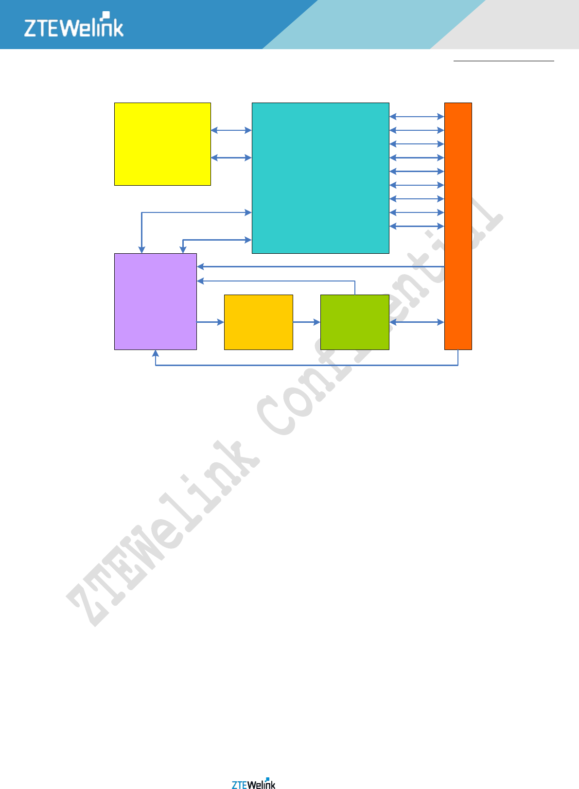
All Rights reserved, No Spreading abroad without Permission 13
ME3631
Hardware Development Guide
--Status interface (LED)
Baseband
USB
USIM
UART
I2C
SDIO
SPI
LED
ADC
GPIO
FLASH
&
LPDDR2
Data
Control
Control
Rx&Tx
RF
Transceiver
RF PA Duplexer
Duplexer
Tx
Rx
MAIN_ANT
80PIN LCC Connector Interface
Rx GNSS
Rx DIV_ANT
Figure 1–1 System Connection Structure
1.4. EVALUATION BOARD
In order to help you to develop applications with ME3631, ZTEWelink supplies an evaluation board (G2000/GE2015), RS-232 to
USB cable, USB data cable, power adapter, antenna and other peripherals to control or test the module. For details, please refer to
the related document [ZTEWelink G2000 Dev Board User Guide] or [ZTEWelink GE2015 Dev Board User Guide].

All Rights reserved, No Spreading abroad without Permission 14
ME3631
Hardware Development Guide
2. APPLICATION INTERFACE
2.1. GENERAL DESCRIPTION
ME3631 is equipped with an 80-pin 0.72mm pitch SMT pads plus 16-pin ground pads and reserved pads that connect to
customer’s cellular application platform. Sub-interface included in these pads is described in detail in the following chapters:
Pin assignment
Pin description
Power supply
Turn on/off scenarios
USIM interface
USB interface
UART interface
Network status indication
ADC interface
WAKEUP_IN signal
WAKEUP_OUT signal
GPIO interface
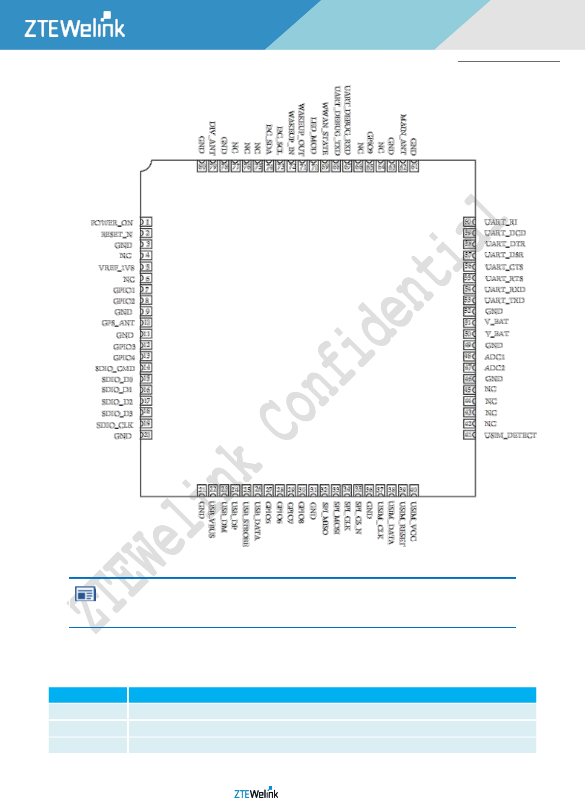
2.2. PIN ASSIGNMENT
The following figure shows the pin assignment of the ME3631 module.
All Rights reserved, No Spreading abroad without Permission 15
ME3631
Hardware Development Guide
Figure 2–1 Pin Assignment
NOTE:
Keep all NC pins unconnected.
2.3. PIN DESCRIPTION
The following table shows the IO Parameters Definition.
Table 2-1 IO Parameters Definition
Type
Description
IO
Bidirectional input/output
DI
Digital input
DO
Digital output
All Rights reserved, No Spreading abroad without Permission 16
ME3631
Hardware Development Guide
PI
Power input
PO
Power output
AI
Analog input
AO
Analog output
OD
Open drain
The logic levels are described in the following table.
Table 2-2 Logic levels Description
Parameter
Min
Max
Unit
VIH
0.65*VDD_IO
VDD_IO+0.3
V
VIL
-0.3
0.35* VDD_IO
V
VOH
VDD_IO-0.45
VDD_IO
V
VOL
0
0.45
V
NOTE:
VDD_IO is the voltage level of pins.
The following tables show the ME3631’s pin definition.
Table 2-3 Pin Description
Power Supply
Pin Name
Pin NO.
I/O
Description
DC Characteristics
Comment
V_BAT
50.51
PI
Power supply for
module
Vmax = 4.2V
Vmin = 3.4V
Vnorm = 3.8V
It must be able to provide
sufficient current in a
transmitting burst which
typically rises to 2.0A
VREF_1V8
5
PO
Provide 1.8V for
external circuit
Vnorm = 1.8V
Imax = 300mA
Power supply for external
GPIO’S pull up circuits
GND
3,9,11,20,21,31,36,
46,49,52, 61,63,78,
80,
Ground
Turn On/Off
Pin Name
Pin NO.
I/O
Description
DC Characteristics
Comment
POWER_ON
1
DI
Turn on/off module
VIH max = 2.1V
VIH min = 1.17V
VIL max = 0.63V
Pull-up to 1.8V through 200K
resistance internally, active low
RESET_N
2
DI
Reset module
VIH max = 2.1V
VIH min = 1.17V
VIL max = 0.63V
Active low
Status Indication
Pin Name
Pin NO.
I/O
Description
DC Characteristics
Comment
LED_MODE
70
DO
Indicate the module
network registration
VOH min = 1.35V
VOL max = 0.45V
1.8V power domain
All Rights reserved, No Spreading abroad without Permission 17
ME3631
Hardware Development Guide
mode
USB Interface
Pin Name
Pin NO.
I/O
Description
DC Characteristics
Comment
USB_DP
24
IO
USB differential data
bus
Compliant with USB
2.0 standard specification
Require differential impedance
of 90Ω
USB_DM
23
IO
USB_VBUS
22
PI
USB power
HSIC Interface
Pin Name
Pin NO.
I/O
Description
DC Characteristics
Comment
USB_STROBE
25
IO
HSIC strobe
InterChip USB(HSIC)
line impedance 50 ohm,
isometric constraint is less than
2 mm, line length is less than
10 cm
USB_DATA
26
IO
HSIC data
USIM Interface
Pin Name
Pin NO.
I/O
Description
DC Characteristics
Comment
USIM_VCC
40
PO
Power supply for
USIM card
For 1.8V USIM:
Vmax = 1.9V
Vmin = 1.7V
For 3.0V USIM:
Vmax = 3.05V
Vmin = 2.7V
IO max = 50mA
Either 1.8V or 3V is supported
by the module automatically
USIM_DATA
38
IO
Data signal of USIM
card
For 1.8V USIM:
VIL max = 0.63V
VIH min = 1.17V
VOL max = 0.45V
VOH min = 1.35V
For 3V USIM:
VIL max = 1.05V
VIH min = 1.95V
VOL max = 0.45V
VOH min = 2.6V
Pull-up to USIM_VCC with 10k
resistor internally
USIM_CLK
37
DO
Clock signal of USIM
card
For 1.8V USIM:
VOL max = 0.45V
VOH min = 1.35V
For 3V USIM:
VOL max = 0.45V
VOH min = 2.6V
USIM_RST
39
DO
Reset signal of USIM
card
For 1.8V USIM:
VOL max = 0.45V
VOH min = 1.35V
For 3V USIM:

All Rights reserved, No Spreading abroad without Permission 18
ME3631
Hardware Development Guide
VOL max = 0.45V
VOH min = 2.6V
USIM_DETECT
41
DI
USIM card input
detection
VIL min = -0.3V
VIL max = 0.63V
VIH min = 1.17V
VIH max = 2.1V
1.8V power domain. Active low
If no need of USIM detect,
leave this pin not connected.
ADC Interface
Pin Name
Pin NO.
I/O
Description
DC Characteristics
Comment
ADC1
48
AI
Analog to digital
0.05V to 4.15V
External sensor signal detection
ADC2
47
AI
Analog to digital
0.05V to 4.15V
External sensor signal detection
Main UART Interface
Pin Name
Pin NO.
I/O
Description
DC Characteristics
Comment
UART_RI
60
DO
Ring indicator
VOL max = 0.45V
VOH min = 1.35V
1.8V power domain, DO not
pull-up external
UART_DCD
59
DO
Data carrier
detection
VOL max = 0.45V
VOH min = 1.35V
1.8V power domain
UART_CTS
56
DI
Clear to send
VOL max = 0.45V
VOH min = 1.35V
1.8V power domain
UART_RTS
55
DO
Request to send
VIL min = -0.3V
VIL max = 0.63V
VIH min = 1.17V
VIH max = 2.1V
1.8V power domain
UART_DTR
58
DI
Data terminal ready
VIL min = -0.3V
VIL max = 0.63V
VIH min = 1.17V
VIH max = 2.1V
1.8V power domain.
UART_DSR
57
DO
Data set ready
VIL min = -0.3V
VIL max = 0.63V
VIH min = 1.17V
VIH max = 2.1V
1.8V power domain.
UART_TXD
53
DO
Transmit data
VOL max = 0.45V
VOH min = 1.35V
1.8V power domain
UART_RXD
54
DI
Receive data
VIL min = -0.3V
VIL max = 0.63V
VIH min = 1.17V
VIH max = 2.1V
1.8V power domain
Debug UART Interface
Pin Name
Pin NO.
I/O
Description
DC Characteristics
Comment
UART_DEBUG_TXD
68
DO
Transmit data
VOL max = 0.45V
VOH min = 1.35V
1.8V power domain
All Rights reserved, No Spreading abroad without Permission 19
ME3631
Hardware Development Guide
UART_DEBUG_RXD
67
DI
Receive data
VIL min = -0.3V
VIL max = 0.63V
VIH min = 1.17V
VIH max = 2.1V
1.8V power domain
RF Interface
Pin Name
Pin NO.
I/O
Description
DC Characteristics
Comment
MAIN_ANT
62
IO
Main antenna
50Ω impedance
DIV_ANT
79
AI
Diversity antenna
50Ω impedance
GNSS_ANT
10
IO
GNSS antenna
50Ω impedance
I2C Interface
Pin Name
Pin NO.
I/O
Description
DC Characteristics
Comment
I2C_SCL
73
DO
I2C serial clock
VOL max = 0.45V
VOH min = 1.35V
Pull-up to 1.8V through
external 2.2K resistance, active
low [can use the power of pin
5]
I2C_SDA
74
IO
I2C serial data
VOL max = 0.45V
VOH min = 1.35V
VIL min = -0.3V
VIL max = 0.63V
VIH min = 1.17V
VIH max = 2.1V
Pull-up to 1.8V through
external 2.2K resistance, active
low [can use the power of pin
5]
SDIO Interface
Pin Name
Pin NO.
I/O
Description
DC Characteristics
Comment
SDIO_CMD
14
IO
Secure digital CMD
VOL max = 0.45V
VOH min = 1.35V
VIL min = -0.3V
VIL max = 0.63V
VIH min = 1.17V
VIH max = 2.1V
Pull-up to 1.8V through
external 10K resistance, active
low [can use the power of pin
5]
SDIO_CLK
19
DO
Secure digital CLK
VOL max = 0.45V
VOH min = 1.35V
1.8V power domain
SDIO_D0
15
IO
Secure digital IO data
bit 0
VOL max = 0.45V
VOH min = 1.35V
VIL min = -0.3V
VIL max = 0.63V
VIH min = 1.17V
VIH max = 2.1V
1.8V power domain
SDIO_D1
16
IO
Secure digital IO data
bit 1
VOL max = 0.45V
VOH min = 1.35V
VIL min = -0.3V
1.8V power domain

All Rights reserved, No Spreading abroad without Permission 20
ME3631
Hardware Development Guide
VIL max = 0.63V
VIH min = 1.17V
VIH max = 2.1V
SDIO_D2
17
IO
Secure digital IO data
bit 2
VOL max = 0.45V
VOH min = 1.35V
VIL min = -0.3V
VIL max = 0.63V
VIH min = 1.17V
VIH max = 2.1V
1.8V power domain
SDIO_D3
18
IO
Secure digital IO data
bit 3
VOL max = 0.45V
VOH min = 1.35V
VIL min = -0.3V
VIL max = 0.63V
VIH min = 1.17V
VIH max = 2.1V
1.8V power domain
SDIO Interface
Pin Name
Pin NO.
I/O
Description
DC Characteristics
Comment
SPI_MISO
32
IO
SPI main input slave
output
VOL max = 0.45V
VOH min = 1.35V
VIL min = -0.3V
VIL max = 0.63V
VIH min = 1.17V
VIH max = 2.1V
1.8V power domain
SPI_MOSI
33
IO
SPI main output slave
input
VOL max = 0.45V
VOH min = 1.35V
VIL min = -0.3V
VIL max = 0.63V
VIH min = 1.17V
VIH max = 2.1V
1.8V power domain
SPI_CLK
34
DO
SPI clock
VOL max = 0.45V
VOH min = 1.35V
1.8V power domain
SPI_CS_N
35
DO
SPI segment
VOL max = 0.45V
VOH min = 1.35V
1.8V power domain
Other Pins
Pin Name
Pin NO.
I/O
Description
DC Characteristics
Comment
WAKEUP_IN
72
DI
Sleep mode control,
External device
wakeup module
VIL min = -0.3V
VIL max = 0.45V
VIH min = 1.53V
VIH max = 2.1V
1.8V power domain. Pull-down
internally. Edge-triggered,
Rising edge wake up module;
Falling edge modules can enter
sleep
WAKEUP_OUT
71
DO
Output wakeup signal,
VOL max = 0.8V
Wakeup external circuits
All Rights reserved, No Spreading abroad without Permission 21
ME3631
Hardware Development Guide
wake up the external
devices
VOH min = 1.35V
GPIO
7, 8, 12, 13,
27, 28, 29, 30,
65,
IO
General input/output
VOL max = 0.45V
VOH min = 1.35V
VIL min = -0.3V
VIL max = 0.63V
VIH min = 1.17V
VIH max = 2.1V
If unused, keep them floating.
DO not pull-up PIN77 external
NC
66,64,75,76,
77,45,44,43,
42,6,4
No connection
NC
2.4. POWER SUPPLY
2.4.1. POWER SUPPLY PINS
The ME3631 is supplied through the V_BAT signal with the following characteristics.
Table 2-4 Power Supply
Pin Name
Pin NO.
Description
Minimum
Typical
Maximum
Unit
V_BAT
50,51
Power supply for module
3.4
3.8
4.2
V
GND
3, 9, 11, 20, 21, 31, 36, 46,
49, 52, 61, 63, 78, 80,
Ground
-
-
GND signal (Pin No: 3/9/11/20/21/31/36/46/49/52/61/63/78/80) is the power and signal ground of the module, which needs
to be connected to the ground on the system board. If the GND signal is not connected completely, the performance of module will
be affected.
2.4.2. DECREASE VOLTAGE DROP
The power supply range of the module is 3.4V~ 4.2V. Because of the voltage drop during the transmitting time, a bypass
capacitor of about 220µF with low ESR should be used. Multi -layer ceramic chip (MLCC) capacitor can provide the best combination
of low ESR. Three ceramic capacitors ((220µF, 22µF、100pF are recommended to be applied to the V_BAT pins. The capacitors should
be placed close to the ME3631’s V_BAT pins. The following figure shows structure of the power supply.
The PCB traces from the V_BAT pins to the power source must be wide enough to ensure that there isn’t too much voltage
drop occurs in the transmitting procedure. The width of V_BAT trace should be no less than 2mm, and the principle of the V_BAT
trace is the longer, the wider.
In poor situation of the network is, the antenna will transmit at the maximum power, and the transient maximum peak current
can reach as high as 2A. So the power supply capacity of system board needs to be above 2.5A to satisfy the requirement of module
peak current; and the average current on the system side needs to be above 0.9A.
2.4.3. REFERENCE CIRCUIT OF POWER SUPPLY
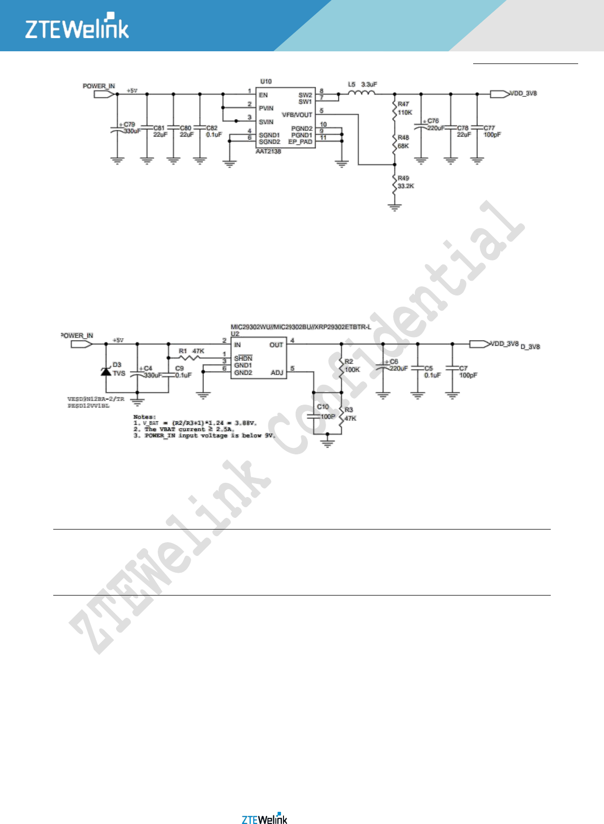
Option One: DC\DC switching
The over-current capability requirement of DC/DC switching power supply needs to be above 2.5A. The reference circuit of
AAT2138 shows as figure below. Place a tantalum capacitor of 330uF at the input of the chip. Place a 220uF and 33uF capacitor
tantalum capacitors at the output of the chip. This circuit fully meets the module power requirements. The current capacity of
inductance L5 is greater than 3A,Please visit http://www.analogictech.com for more information of AAT2138.
All Rights reserved, No Spreading abroad without Permission 22
ME3631
Hardware Development Guide
Figure 2–2 Reference circuit of AAT2138
Option Two: LDO
The over-current capability of LDO is above 2.5A.
As the poor transient response of linear regulator, large capacitors should be placed at the input and output of LDO, place a
capacitor above 220uF at output of LDO,R2、R3 recommend 1% accuracy. The reference power supply circuit design with LDO is
shown as figure below:
Figure 2–3 Reference circuit of LDO
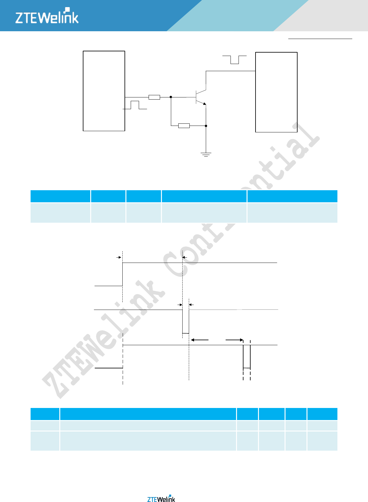
2.5. TURN ON SCENARIOS
When MCU can provide high level pulse with adjustable length, A reference circuit to turn-on/off module is
as shown in the following figure below.
NOTE:
The resistors R1 and R2 in Figures below are only the recommended value and they need to adjust according
to the actual situation.
All Rights reserved, No Spreading abroad without Permission 23
ME3631
Hardware Development Guide
Power_on/off
pulse R2
R1
GPIO from
host
4.7K
47K
POWER_ON
Module
pin1
MCU
Figure 2–4 reference circuit to turn-on/off module(1)
The following table shows the pin definition of POWER_ON/OFF.
Table 2-5 POWER_ON/OFF Pin Description
Pin Name
Pin NO.
I/O
Description
Comment
POWER_ON
1
DI
Turn on/off the module
low active. Pull-up to 1.8V through 200K
resistance internally
The power on scenarios is illustrated as the following figure, the module will power on and working when the POWER_ON pin
keep in low level, in this process , please ensure VBAT steady.
VBAT
POWER_ON
T1
Ensure VBAT steady
T2
RESET_N
Figure 2–5 Timing of Turning on Mode
Table 2-6 Power-on Time
Parameter
Description
Min
Typical
Max
Unit
T1
The period that the Power-on signal for power on operation is kept on the low PWL
0.1
0.2
--
Second
T2
The minimum interval between the POWER_ON and RESET signals if you want to
reset the module after power-on.
10
15
--
Second
All Rights reserved, No Spreading abroad without Permission 24
ME3631
Hardware Development Guide
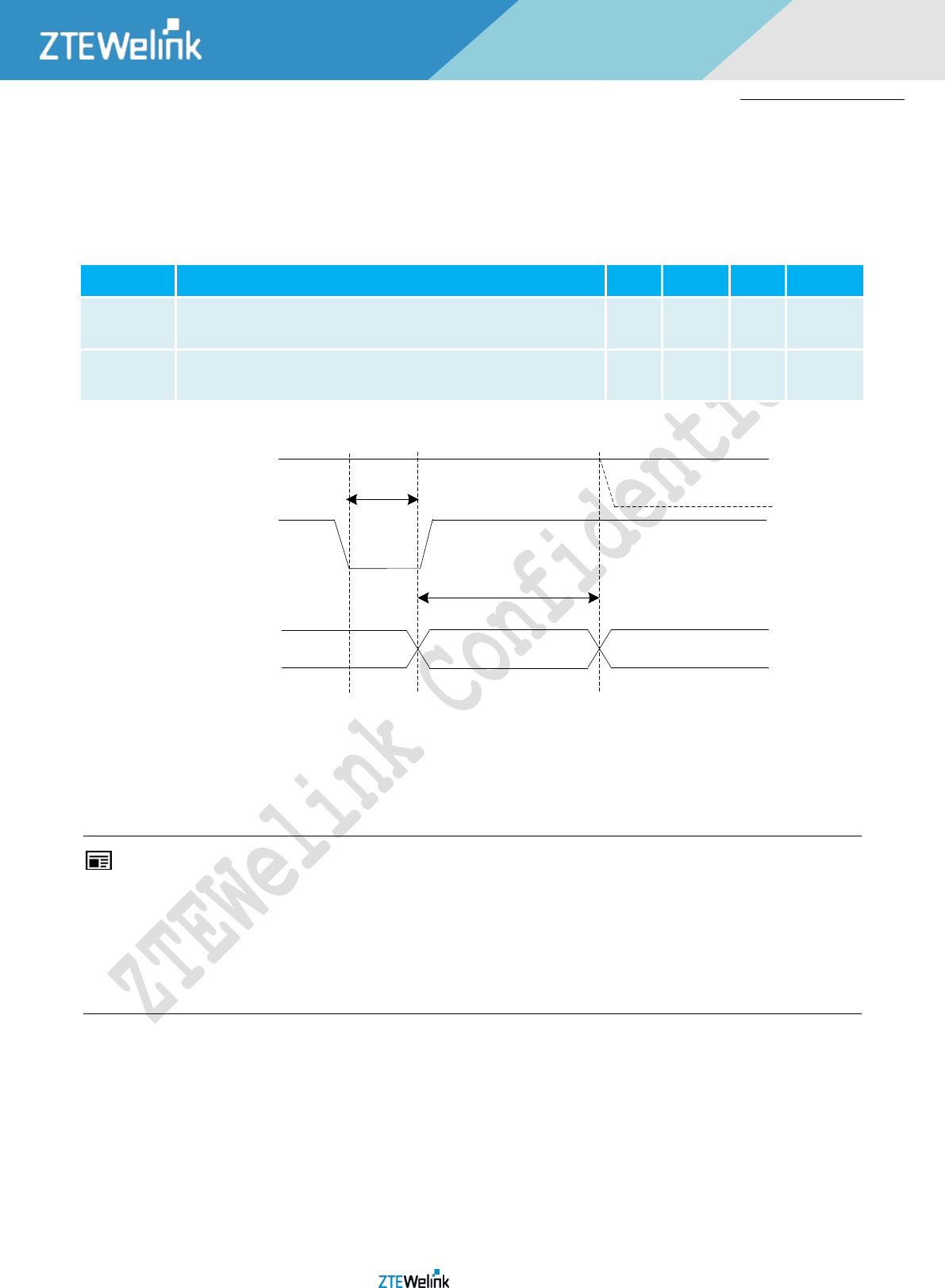
2.6. TURN OFF SCENARIOS
The module supports two modes to turn off:
Mode 1:
Pull down pin1 (POWER_ON) for 2.5-3s will turn off the module. The power off process will take 22s at least.
The reference circuit can refer to the figure 2-4.
Parameter
Description
Min
Typical
Max
Unit
T2
The period that the POWER_ON signal for power off operation is
kept on the low PWL
2.5
3
--
second
T3
The period that the VBAT signal should be kept after power off
operation is down
22
--
--
second
VBAT
high level
POWER_ON
Module
Status Turning offRunning
T2
T3
Power off
Figure 2–6 Timing of Turning off Mode
Mode 2:
Send command of AT+ZTURNOFF, and the power off process will take 15s at least.
Note:when using modules, you need to avoid power off abnormally and frequently, as it will cause several risks
shwon as below:
1. it will damage the flash permanently.
2. it can’t send deregiter message to e-NodeB, and the MMS takes for the module is still registering to network, and it
won’t remind “the user can’t reach” or “the user has turn down” when it’s called(MT).
2.7. RESET SCENARIOS
Mode 1:
When the software stops response, you can pulled down RESIN_N pin(pin2) for 1 sencod to reset the
module's system.
When MCU can provide high level pulse with 1 second, A reference circuit to reset module is as shown in the
following figure below.
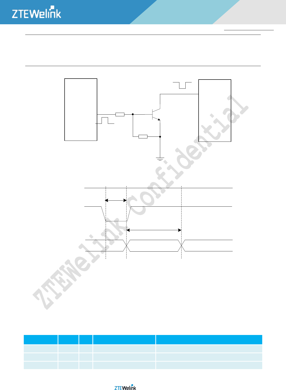
All Rights reserved, No Spreading abroad without Permission 25
ME3631
Hardware Development Guide
NOTE:
The resistors R1 and R2 in Figures below are only the recommended value and they need to adjust according
to the actual situation.
1s
Reset pulse
R2
R1
GPIO from
host
4.7K
47K
RESET_N
Module
pin2
MCU
Figure 2–7 reference circuit to reset module(1)
The reset scenario is illustrated as the following figure,
VBAT
high level
RESET_N
Module
Status ResettingRunning Running
1s
COM can
send/receive AT
32s
Figure 2–8 Timing of Reset Mode
Mode 2:
Send command of AT+ZRST, and the RESET process until the AT port can communicate will take 27s at least.
2.8. USIM CARD INTERFACE
2.8.1. DESCRIPTION OF PINS
The USIM card interface circuitry meets ETSI and IMT-2000 SIM interface requirements. Both 1.8V and 3.0V USIM cards are
supported.
Table 2-7 Pin Definition of the USIM Interface
Pin Name
Pin NO.
I/O
Description
Comment
USIM_VCC
40
PO
Power supply for USIM card
Either 1.8V or 3V is supported by the module automatically
USIM_DATA
38
IO
Data signal of USIM card
Pull-up to USIM_VDD with 10k resistor internally
USIM_CLK
37
DO
Clock signal of USIM card
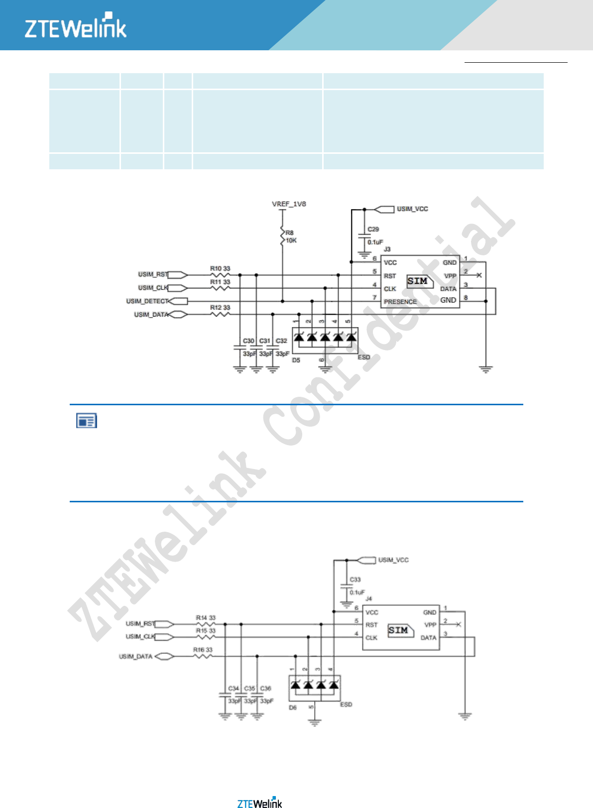
All Rights reserved, No Spreading abroad without Permission 26
ME3631
Hardware Development Guide
USIM_RST
39
DO
Reset signal of USIM card
USIM_DETECT
41
DI
USIM card hot swap detection pin.
1.8V power domain. The signal is internally pulled up.
Keep USIM_DETECT not connected, if it is not used. When USIM
detect function is enable (send AT command AT+ZSDT=1), and if
it is Low, USIM is present; if it is High, USIM is absent.
GND
36
Ground
The following figure shows the reference design of the 8-pin USIM card.
Figure 2–9 Reference Circuit of the 8 Pin USIM Card
NOTE:
R10~R12 and D5 are applied to suppress the EMI spurious transmission and enhance the ESD
protection.Should be closed to J3.
USIM_DETECT is used to detect USIM card, which will be low when the USIM card is inserted.
The value of C29 shoule be less than 1uF
ME3631 supports USIM card hot-plugging via the USIM_ DETECT pin. For details, refer to document [AT Command Reference
Guide of Module Product ME3631_V1.0]. If you do not need the USIM card detect function, keep USIM_ DETECT unconnected.
The reference circuit for using a 6-pin USIM card socket is illustrated as the following figure.
Figure 2–10 Reference Circuit of the 6 Pin USIM Card
All Rights reserved, No Spreading abroad without Permission 27
ME3631
Hardware Development Guide
NOTE:
R14~R16 and D6 are applied to suppress the EMI spurious transmission and enhance the ESD
protection.D6 should be closed to J4
The value of C33 shoule be less than 1uF.
In order to enhance the reliability and availability of the USIM card in customer’s application, please follow the following
criterion in the USIM circuit design:
Keep layout of USIM card as close as possible to the module. Assure the possibility of the length of the trace is less than
50mm.
Keep USIM card signal away from RF and V_BAT alignment.
Assure the ground between module and USIM cassette short and wide. Keep the width of ground and USIM_VCC no less
than 0.5mm to maintain the same electric potential. The decouple capacitor of USIM_VCC should be less than 1uF and
must be near to USIM cassette.
To avoid cross-talk between USIM_DATA and USIM_CLK, keep them away with each other and shield them with
surrounded ground.
In order to offer good ESD protection, it is recommended to add TVS such as WILL (http://www.willsemi.com)
ESDA6V8AV6. The 33Ω resistors should be added in series between the module and the USIM card so as to suppress the
EMI spurious transmission and enhance the ESD protection. Please note that the USIM peripheral circuit should be close
to the USIM card socket.
The pull-up resistor on USIM_DATA line can improve anti-jamming capability when long layout trace and sensitive
occasion is applied.
2.8.2. DESIGN CONSIDERATIONS FOR USIM CARD HOLDER
For 8-pin USIM card holder, it is recommended to use Molex 91228.
Please visit http://www.molex.com for more information.
All Rights reserved, No Spreading abroad without Permission 28
ME3631
Hardware Development Guide
Figure 2–11 Molex 91228 USIM Card Holder
Table 2-8 Pin Description of Molex USIM Card Holder
Pin Name
Pin NO.
Function
GND
1
Ground
VPP
2
Not connected
DATA I/O
3
USIM card data
CLK
4
USIM card clock
RST
5
USIM card reset
VDD
6
USIM card power supply
DETECT
7
USIM card Detection
NC
8
Not defined, Connect to Ground
For 6-pin USIM card holder, it is recommended to use Amphenol C707 10M006 512 2.
Please visit http://www.amphenol.com for more information.
All Rights reserved, No Spreading abroad without Permission 29
ME3631
Hardware Development Guide
Figure 2–12 Amphenol C707 10M006 512 2 USIM Card Holder
Table 2-9 Pin Description of Amphenol USIM Card Holder
Pin Name
Pin NO.
Function
GND
1
Ground
VPP
2
Not connected
DATA I/O
3
USIM card data
CLK
4
USIM card clock
RST
5
USIM card reset
VDD
6
USIM card power supply
2.9. USB INTERFACE
ME3631 contains one integrated USB transceiver which complies with the USB 2.0 specification and supports high speed (480
Mbps), full speed (12 Mbps) and low speed (1.5 Mbps) mode. The USB interface is primarily used for AT command, data transmission,
software debug and firmware upgrade. The following table shows the pin definition of USB interface.
All Rights reserved, No Spreading abroad without Permission 30
ME3631
Hardware Development Guide
Table 2-10 USB Pin Description
Pin Name
Pin NO.
I/O
Description
Comment
USB_DP
24
IO
USB differential data bus (positive)
Require differential impedance of 90Ω
USB_DM
23
IO
USB differential data bus (negative)
Require differential impedance of 90Ω
USB_VBUS
22
PI
USB power
USB plug detect
GND
21
Ground
More details about the USB 2.0 specifications, please visit http://www.usb.org/home.
For different use purposes, different designs can be referred to:
When USB is not the desired function, connect differential signal, power and GND via test points.
Connect USB interface to USB connector directly. The following figure shows the reference circuit of USB interface.
MODULE
USB_ DP
USB_ DM
USB_ VBUS
GND
USB
connector
USB_ DP
USB_ DM
USB_ VBUS
GND
ESD
Figure 2–13 Reference Circuit of USB Application
Reference Circuit of USB Communication between module and AP is the one below. The 0Ω in the figure should be placed near pin.
MODULE
USB_DP
USB_DM
USB_VBUS
GND
USB
connector
USB_DP
USB_DM
USB_VBUS
GND
Figure 2–14 Reference Circuit of USB Communication between module and AP
In order to ensure the USB interface design corresponding with the USB 2.0 specification, please comply with the following
principles.
It is important to route the USB signal traces as differential pairs with total grounding. The impedance of USB differential trace
is 90ohm.
Pay attention to the influence of junction capacitance of ESD component on USB data lines. Typically, the capacitance value
should be less than 2pF.
Do not route signal traces under crystals, oscillators, magnetic devices and RF signal traces. It is important to route the USB
differential traces in inner-layer with ground shielding not only upper and lower layer but also right and left side.
Keep the ESD components as closer to the USB connector as possible.
2.10. UART INTERFACE
The module provides two UART interfaces: Main UART Port and Debug UART Port. The Main UART Port can work in full
All Rights reserved, No Spreading abroad without Permission 31
ME3631
Hardware Development Guide
function mode while the Debug UART Port is used for software debugging or Firmware upgrade. The following show the different
features.
Main UART interface support 2400 4800 9600 19200 38400 57600 115200 460800 921600 1000000 1152000 1500000 2000000
2500000 3000000 3500000bps baud rate, the default is 115200bps, This interface can be used for data transmission; AT
communication or firmware upgrade (upgrade is not supported currently).
Debug UART interface supports 115200bps baud rate. It can be used for software debug and firmware upgrade. The module is
designed as the DCE (Data Communication Equipment), following the traditional DCE-DTE (Data Terminal Equipment) connection.
The following tables show the pin definition of these two UART interfaces.
Table 2-11 Pin Definition of the Main UART Interface
Pin Name
Pin NO.
I/O
Description
Comment
UART_RI
60
DO
Ring indicator
1.8V power domain
UART_DCD
59
DO
Data carrier detection
1.8V power domain
UART_CTS
56
DI
Clear to send
1.8V power domain
UART_RTS
55
DO
Request to send
1.8V power domain
UART_DTR
58
DI
Data terminal ready
1.8V power domain.
UART_DSR
57
DO
Data set ready
1.8V power domain.
UART_TXD
53
DO
Transmit data
1.8V power domain
UART_RXD
54
DI
Receive data
1.8V power domain
Table 2-12 Pin Definition of the Debug UART Interface
Pin Name
Pin NO.
I/O
Description
Comment
UART_DEBUG_TXD
68
DO
Transmit data
1.8V power domain
UART_DEBUG_RXD
67
DI
Receive data
1.8V power domain
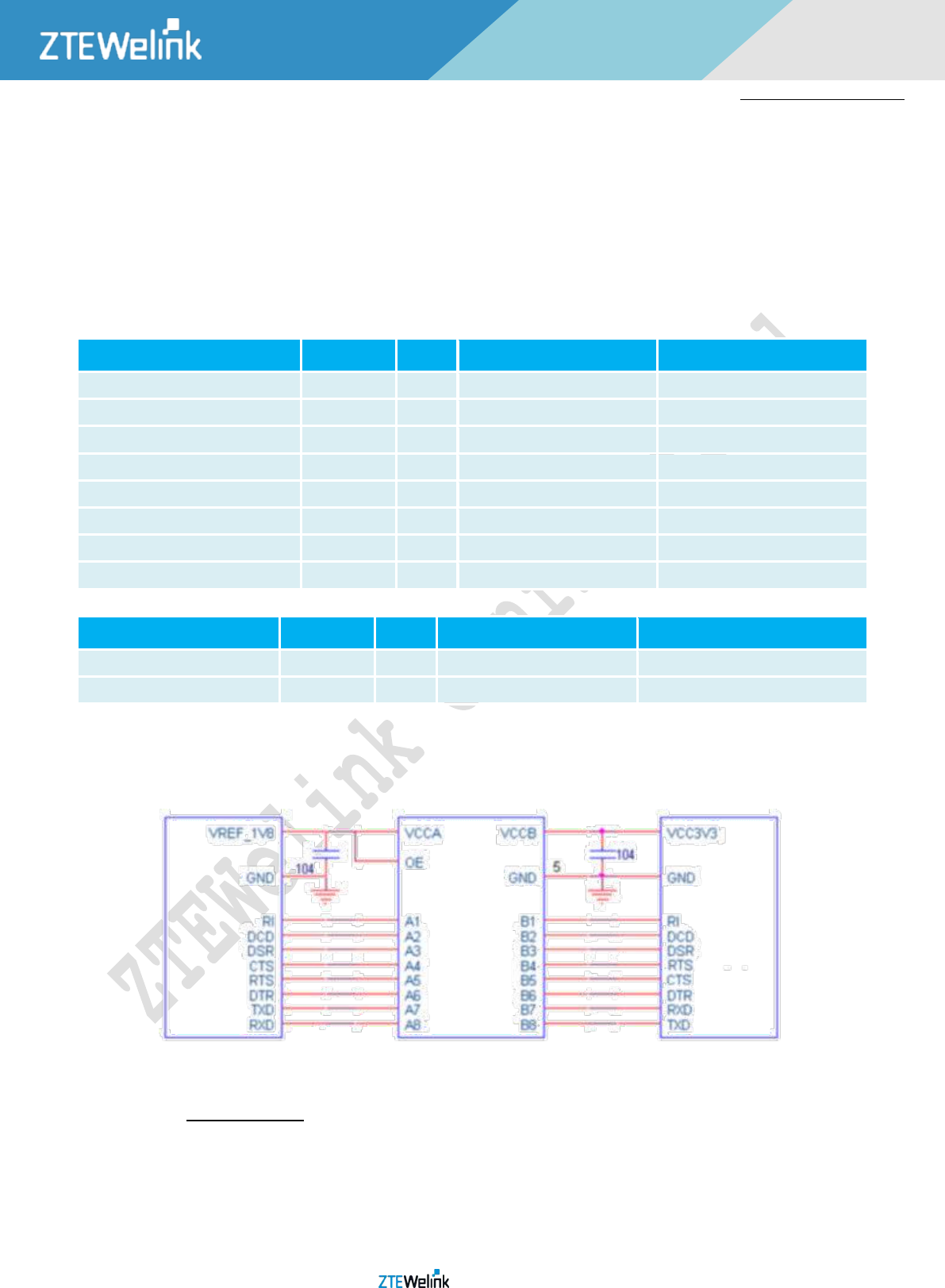
Reference Circuit of Logic Level Translator
ME3631 provides you with a 1.8V UART interface. A level shifter should be used if your application is equipped with a 3.3V
UART interface. A level shifter TXB0108PWR provided by Texas Instruments is recommended. The following figure shows the
reference design of the TXB0108PWR.
Module TXB0108PWR MCU
Figure 2–15 Reference Circuit of Logic Level Translator
Please visit http://www.ti.com for more information.
A. Reference Circuit between ME3631 and PC
The following figure is an example of connection between ME3631 and PC. A voltage level translator and a RS-232 level
translator chip must be inserted between module and PC, since these two UART interfaces do not support the RS-232 level, while
support the 1.8V CMOS level only.
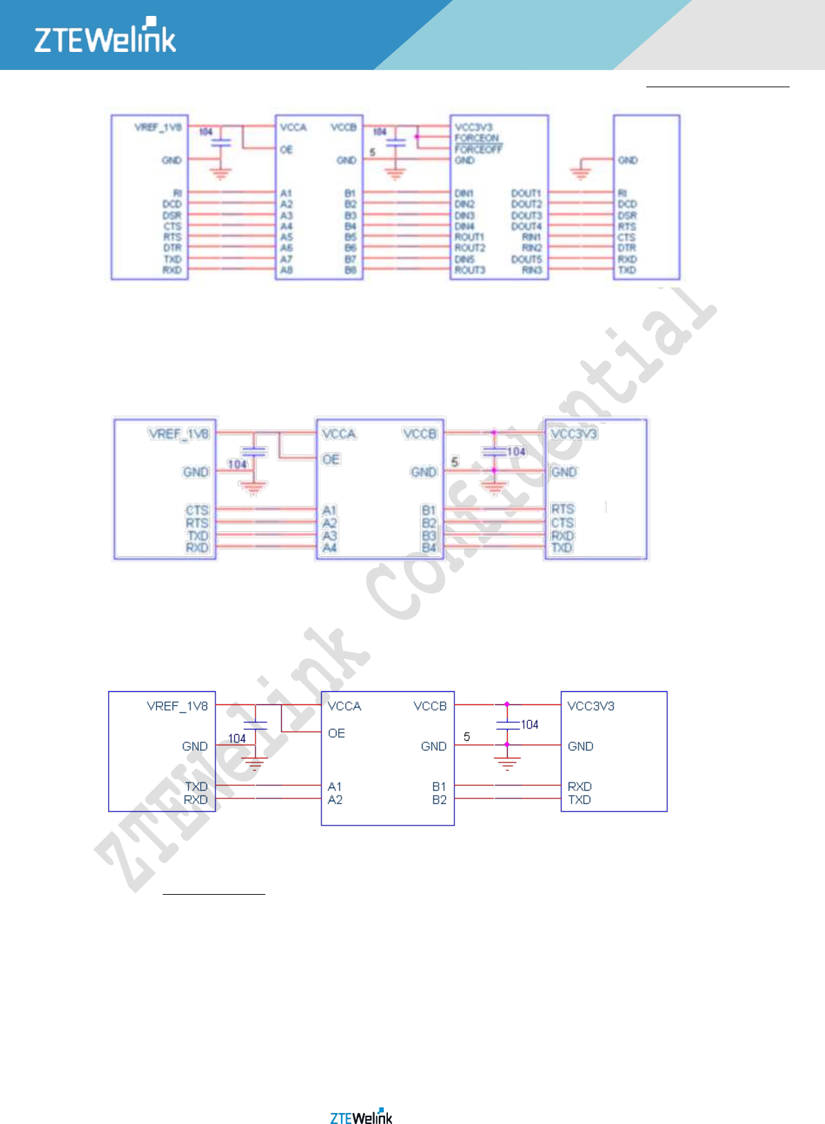
All Rights reserved, No Spreading abroad without Permission 32
ME3631
Hardware Development Guide
Module TXB0108PWR MAX3238 DB9 to PC
Figure 2–16 RS232 Level Match Circuit
B. Reference Circuit of Main URAT Port to 4 Line UART Port
The following figure shows the reference circuit of main UART interface with 4 line logic level translator. TXB0104PWR
provided by Texas Instruments is recommended.
Module TXB0104PWR MCU
Figure 2–17 Reference Circuit of Main UART with 4 Line Level Translator
Reference Circuit of URAT Port to 2 line UART Port
The following figure shows the reference circuit of UART interfaces with 2 line logic level translator. TXB0102DCU provided by
Texas Instruments is recommended.
Module TXB0102DCU MCU
Figure 2–18 Reference Circuit of UART with 2 Line Level Translator
Please visit http://www.ti.com for more information.
C. Debugging UART port
Debugging UART port is a 2-wire interface. It should be connected with its test point or jumper pin during design.
2.11. NETWORK STATUS INDICATION
The network indication pin LED_MODE can be used to drive a network status indicator LED. The different modes of status
indicator flashing indicate different network statuses. The following tables describe pin definition and logic level changes in different
network status.
All Rights reserved, No Spreading abroad without Permission 33
ME3631
Hardware Development Guide
Table 2-13 Pin Definition of Network Indicator
Pin Name
Pin NO.
I/O
Description
Comment
LED_MODE
70
DO
Indicate the module network registration mode
1.8V power domain
Table 2-14 Working State of the Network Indicator
LED Status
Module status
High level, LED on
Module register to network success
Low level, LED off
Module not register to network(module is in flight mode or power off)
Low level 1s(LED off), High level 1s(LED on)
PDP activated, and get the IP address or Socket established
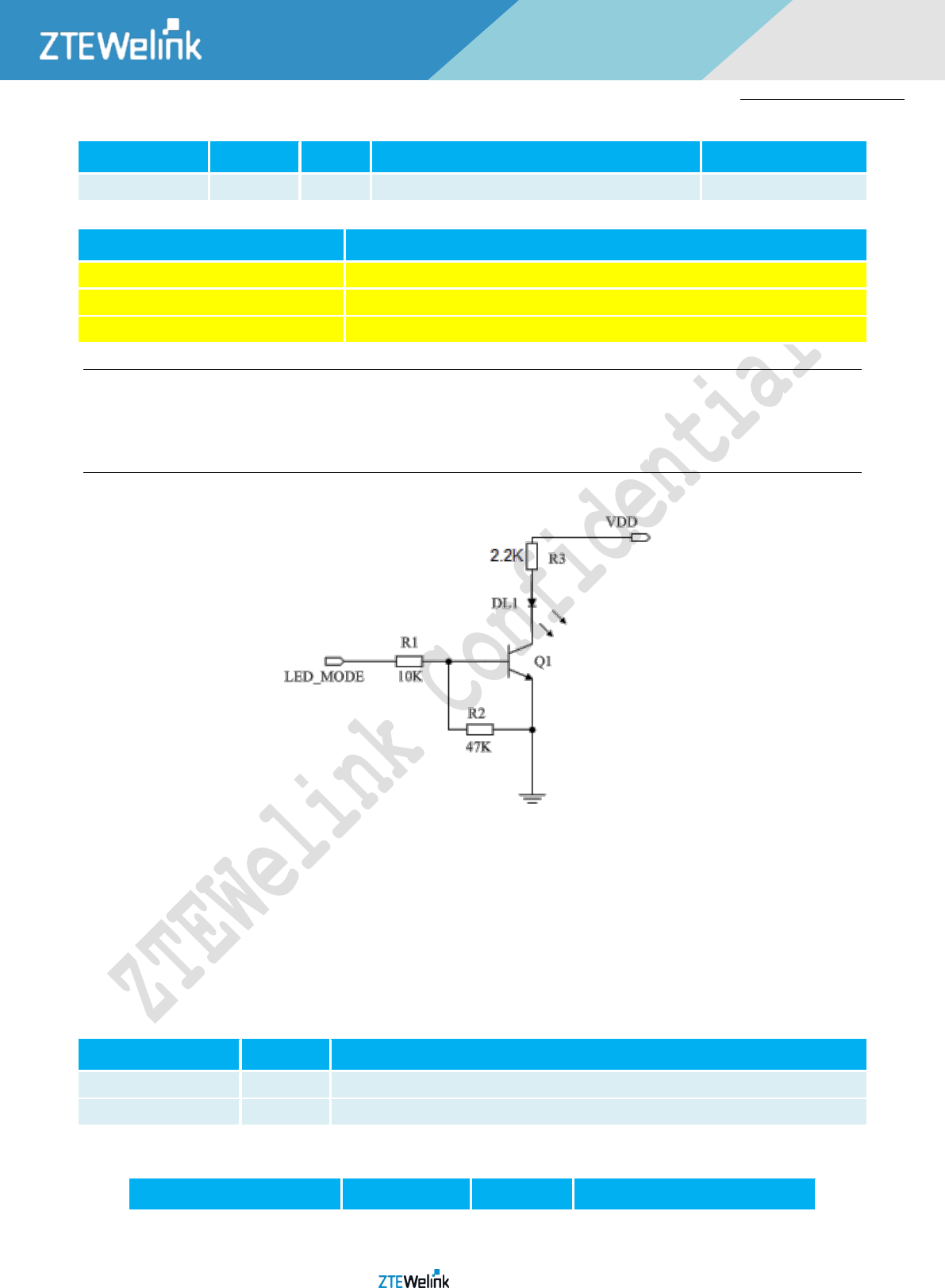
Figure below is the reference circuit design diagram.
NOTE:
The resistors R1, R2 and R3 in Figures below are only the recommended value and they need to adjust
according to the actual situation.
Figure 2–19 Reference Circuit of the Network Indicator
2.12. ADC INTERFACE
The module provides two ADCs to digitize the analog signal to 10-bit digital data such as battery voltage, temperature and so
on. Using AT command “AT+ZADC1?” can read the voltage value on ADC1 pin. Using AT command “AT+ZADC2?” can read the voltage
value on ADC2 pin. The read value is expressed in mV. For more details of these AT commands, please refer to document [AT
Command Reference Guide of Module Product ME3631_V1.0].
In order to improve the accuracy of ADC, the trace of ADC should be surrounded by ground.
Table 2-15 Pin Definition of the ADC
Pin Name
Pin NO.
Description
ADC1
48
General purpose analog to digital converter.
ADC2
47
General purpose analog to digital converter.
The following table describes the characteristic of the ADC function.
Table 2-16 Characteristic of the ADC
Item
Min
Max
Unit
All Rights reserved, No Spreading abroad without Permission 34
ME3631
Hardware Development Guide
ADC1 voltage range
0.05
4.15
V
ADC2 voltage range
0.05
4.15
V
ADC resolution
15
Bits
2.13. WAKEUP_IN SIGNAL
The module provides an AP control interface for communicating with external Application Processor including WAKEUP_IN.
The following table shows the pin definition of AP control interface.
Table 2-17 Pin Definition of WAKEUP_IN
Pin Name
Pin NO.
I/O
Description
Comment
WAKEUP_IN
71
DI
Input control signal
1.8V power domain. Pull-down internally. Edge-triggered, Rising
edge wake up module; Falling edge modules can enter sleep
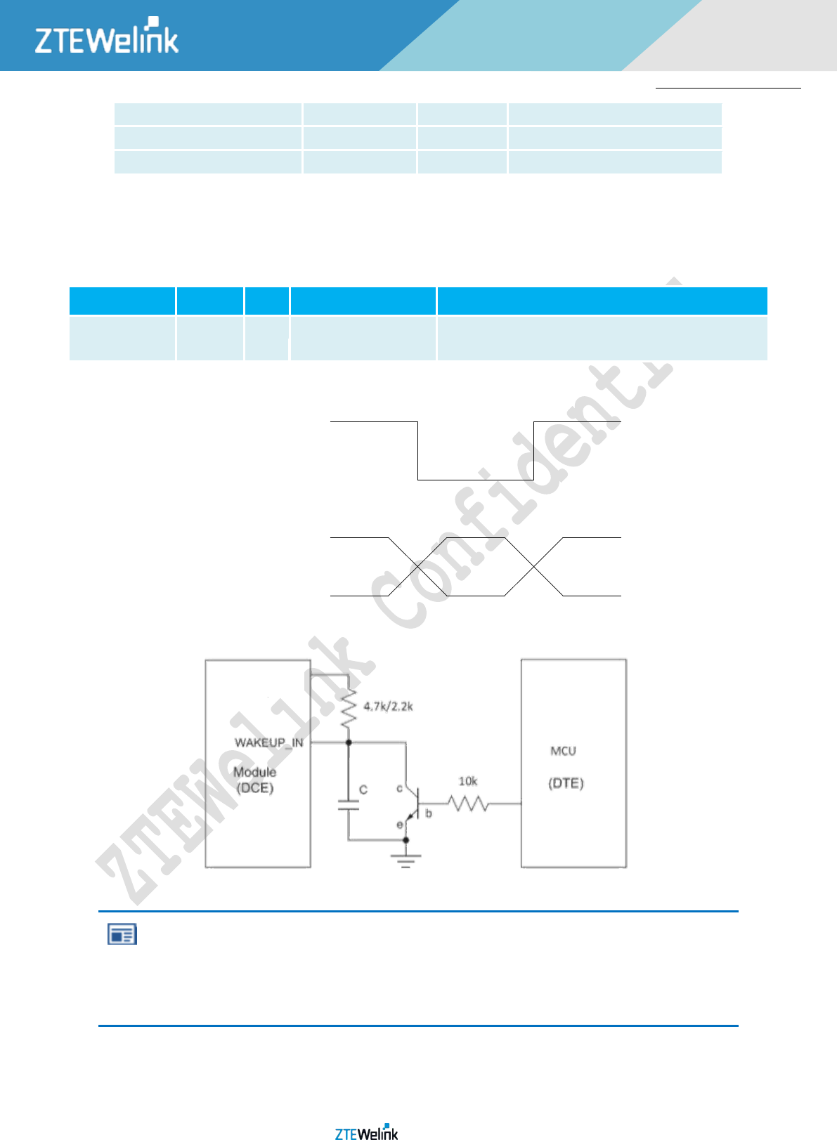
When the module needs to be waken up, input a related signal via WAKEUP-IN. The following figure is the signal waveform:
WAKEUP_IN:
High
Low
Module state:Sleep state Operating state
High
Operating state
Figure 2–20 WAKEUP_IN input sequence
Figure 2–21 Connections of the WAKEUP_IN pin
NOTE:
There is Anti-shake design with WAKEUP_IN pin internal, when pull up or down this pin by external
processor, the level must last more than 500ms. WAKEUP_IN Usage scenario you can refer to the
document named ZTEWelink ME3631 Module Power Management Design Guide.pdf
VREF_1V8
All Rights reserved, No Spreading abroad without Permission 35
ME3631
Hardware Development Guide
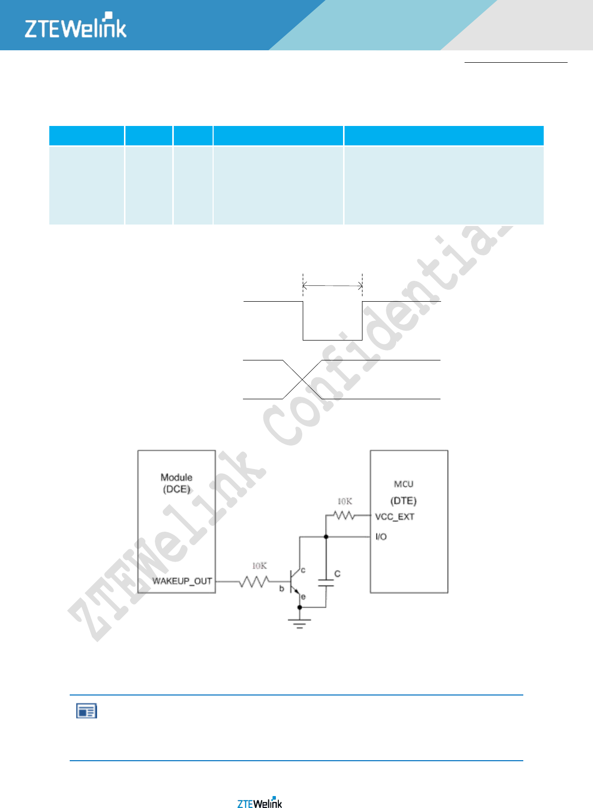
2.14. WAKEUP_OUT SIGNAL
The module provides the WAKEUP_OUT pin which is used to wake up the external devices.
Table 2-18 Pin Definition of WAKEUP_OUT
Pin Name
Pin NO.
I/O
Description
Comment
WAKEUP_OUT
71
DO
Output wakeup signal
1.8V power domain
The pin output a high-level voltage by default. When a
wake-up source (such as new SMS receive, call, network
data ) arrives, the pin output a low-level-voltage pulse
lasting for 1s
For instance, When a wake-up source arrives, the module will output the level shown as the figure below through pin 71.
Module state:Operating state
Sleep state
low
High
WAKEUP_OUT:
1s
Figure 2–22 The output signal of WAKEUP_OUT
Figure 2–23 Connections of the WAKEUP_OUT pin
NOTE:
WAKEUP_OUT Usage scenario you can refer to the document named ZTEWelink ME3631 Module Power
Management Design Guide.pdf
All Rights reserved, No Spreading abroad without Permission 36
ME3631
Hardware Development Guide
2.15. GPIO INTERFACE(NOT SUPPORT YET)
Module provides 9 GPIO pins. The direction and output voltage level of the GPIO can be set by AT command “AT+ZGPIO”. The
input voltage level of the GPIO can also be read by AT command “AT+ZGPIO”. For more details of these AT commands, please refer to
document [AT Command Reference Guide of Module Product ME3631_V1.0].
Table 2-19 Pin Definition of GPIO
Pin Name
Pin NO.
I/O
Description
Comment
GPIO1
7
IO
General input/output
1.8V power domain
GPIO2
8
IO
General input/output
1.8V power domain
GPIO3
12
IO
General input/output
1.8V power domain
GPIO4
13
IO
General input/output
1.8V power domain
GPIO5
27
IO
General input/output
1.8V power domain
GPIO6
28
IO
General input/output
1.8V power domain
GPIO7
29
IO
General input/output
1.8V power domain
GPIO8
30
IO
General input/output
1.8V power domain
GPIO9
65
IO
General input/output
1.8V power domain
All Rights reserved, No Spreading abroad without Permission 37
ME3631
Hardware Development Guide
3. ANTENNA INTERFACE
ME3631 antenna interface includes a main antenna, an Rx-diversity antenna and a GNSS antenna to improve receiving
performance. The antenna interface has an impedance of 50Ω.
3.1. PIN DEFINITION
The main antenna and Rx-diversity antenna pins definition are shown below.
Table 3-1 Pin Definition of GPIO
Pin Name
Pin NO.
I/O
Description
Comment
MAIN_ANT
62
IO
Main antenna
50Ω impedance
DIV_ANT
79
AI
Diversity antenna
50Ω impedance
GNSS_ANT
10
IO
GNSS antenna
50Ω impedance
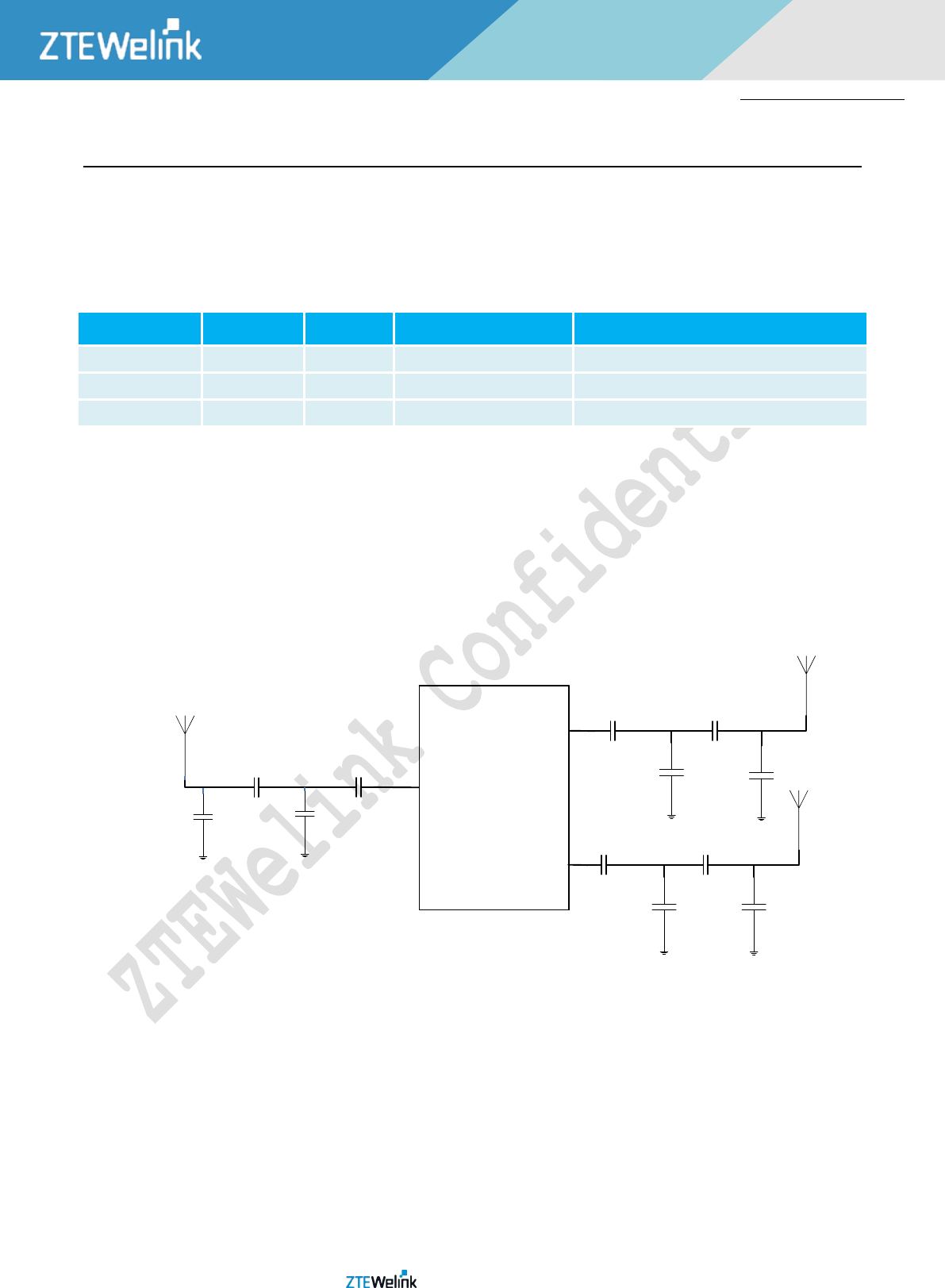
3.2. REFERENCE DESIGN
The antenna is a sensitive device and its performance is greatly affected by external environments. The radiation performance
of the antenna is affected by the module dimensions, antenna position, occupied space size of the antenna, and the grounding of
surrounding components of the antenna. Besides, the fixed assembly of the antenna, the wiring of RF cables on the antenna, and the
fixed position of the antenna all affect the radiation performance of the antenna too.
The reference design of main antenna and Rx-diversity antenna is shown as below. It should reserve a double-L-type matching
circuit for better RF performance, and place these components as close as possible to the module. The capacitors are not mounted
by default.
MAIN_ANT
DIV_ANT
GNSS_ANT
33pF
NC
NC
NC
NC
NC
33pF
33pF
33pF
33pF33pF
NC
Figure 3–1 Reference Circuit of Antenna Interface
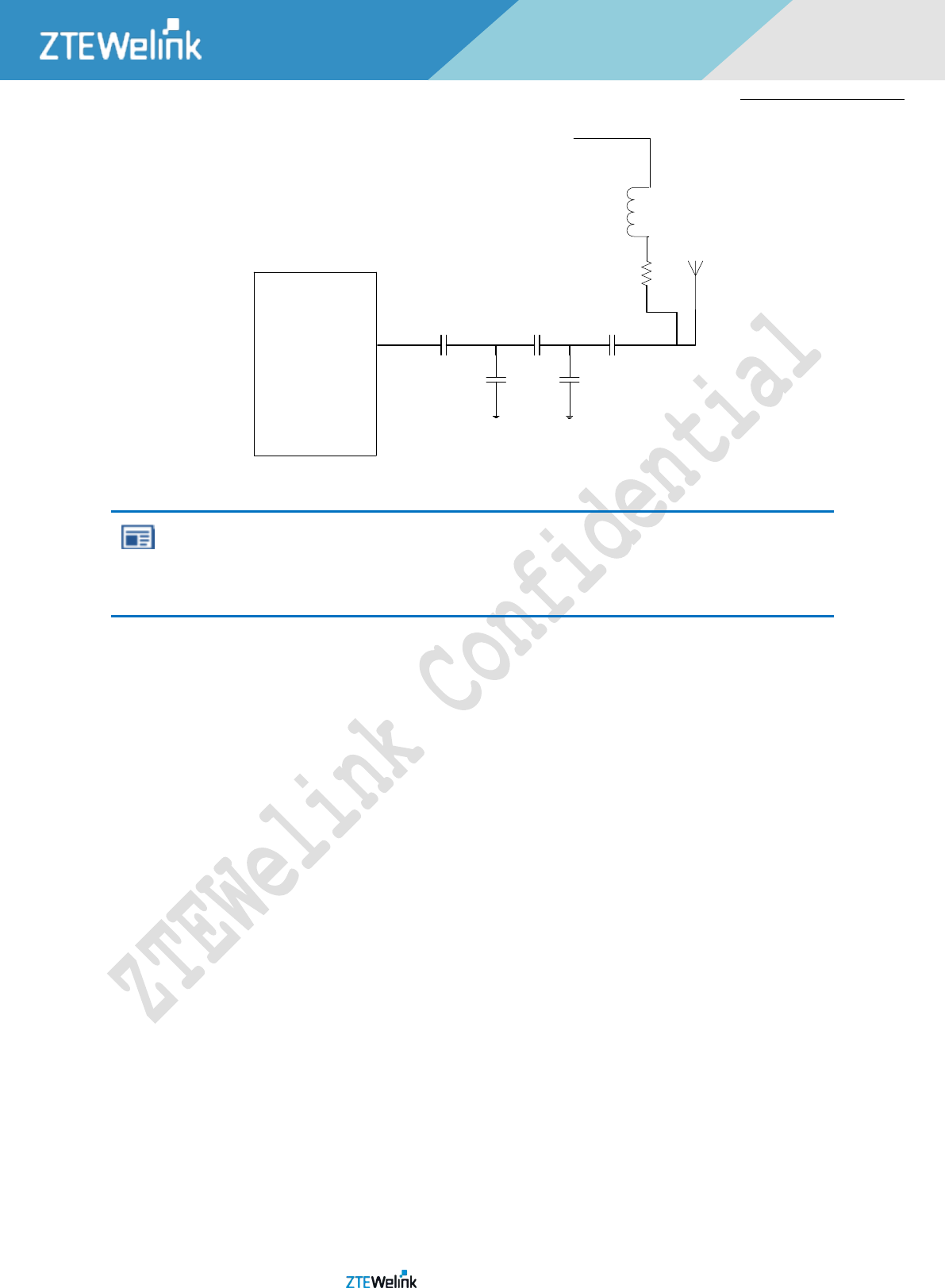
The following picture is the reference of GNSS active antenna, VDD is its power, power supply should be designed by actual
requirements.
All Rights reserved, No Spreading abroad without Permission 38
ME3631
Hardware Development Guide
C2
L2
L1
C3
VDD
GNSS_ANT
MODULE
R1
L3
C1
Figure 3–2 Reference Circuit of GNSS Antenna
NOTE:
Keep a proper distance between main and diversity antenna to improve the receiving sensitivity. GNSS
and Rx-diversity are not supported by C1B; therefore GNNS antenna design is not concerned in C1B type.
3.3. REFERENCE PCB LAYOUT OF ANTENNA
Please follow the following criterion in the process of antenna line PCB layout design:
Make sure that the transmission line’s characteristic impedance is 50ohm;
Keep line on the PCB as short as possible, since the antenna line loss shall be less than 0.3 dB;
Line geometry should have uniform characteristics, constant cross section, avoid meanders and abrupt curves;
It is wise to surround the PCB transmission line with ground, avoid having other signal tracks facing directly the antenna line
track.
Keep at least one layer of the PCB used only for the ground plane; and use this layer as reference ground plane for the
transmission line;
The ground surrounding the antenna line on PCB has to be strictly connected to the main Ground Plane by means of via
holes (once per 2mm at least), placed close to the ground edges facing line track;
Place EMI noisy devices as far as possible from modules antenna line;
Keep the antenna line far away from the module power supply lines;
3.4. SUGGESTIONS FOR EMC & ESD DESIGN
3.4.1. EMC DESIGN REQUIREMENTS
During the design of the whole device, the user needs to fully consider the EMC problem caused by the signal integrity and
power integrity.
During the product design, it is better to separate the module from the mainboard PCB, instead of installing the module on the
ground of the mainboard. If they cannot be separated, the module should be far from modules and components that might generate
EMI, such as chip and memory, power interface, and data cable interface.
Because the mainboard of PAD, CPE, and Internet laptops does not have a shielding cover, as that of mobile terminals, to shield
most circuits to avoid overflow of electromagnetic interference, you can spray conductive paint on the surface on non-antenna areas
within the structural components above and below the mainboard, and the conductive paint should be connected to the ground on
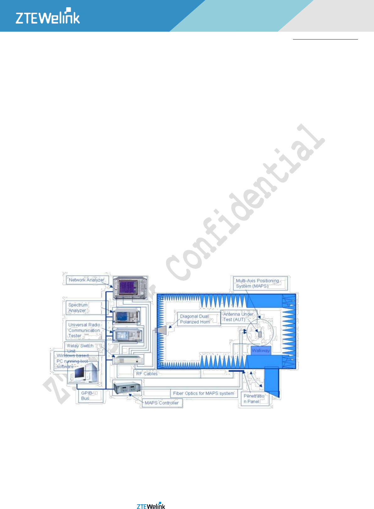
All Rights reserved, No Spreading abroad without Permission 39
ME3631
Hardware Development Guide
the mainboard by several points to shield electromagnetic interference.
Besides, data cables of the LCD and the camera might introduce interference signals, which affect the receiving performance of
the antenna. Thus, it is necessary to wrap conductive cloth around the two data cables and connected them to the ground.
RF cables of the antenna should be far from modules and components that might generate EMI, such as chip and memory,
power interface, and data cable interface. The wiring of RF cables should be close to the ground of the mainboard.
During the layout and wiring of peripheral circuits, for the wiring of power and signal cables, keep a distance of 2 times of the
line width, so as to effectively reduce the coupling between signals and keep a clean reflux path for the signal.
During the design of peripheral power circuits, the de-coupled capacitor should be placed closed to the module power PIN, the
high-frequency high-speed circuit and the sensitive circuit should be placed far away from the border of PCB. They should better be
separated during layout, so as to reduce the interference between them and protect the sensitive signal.
For the circuit or device on the side of system board that might interfere with the module, it should be shielded during design.
3.4.2. ESD DESIGN REQUIREMENTS
Module is embedded on the side of system board, so the user needs to make the ESD protection during design. For the key
input/output signal interface, such as the (U)SIM card signal interface, the ESD device should be placed closely for protection.
Besides, on the side of main board, the user should reasonably design the structure and PCB layout, guarantee that the metallic
shielding shell is fully grounded, so as to leave a smooth discharge channel for ESD.
3.5. TEST METHODS FOR WHOLE-SET ANTENNA OTA
Figure below is the diagram of OTA test system of CTIA. The system is mainly composed of test chamber, high-precision
positioning system and its controller, Windows based PC running test software and RF test instruments with automatic test program.
The main RF instruments are integrated RF test equipment, Spectrum Analyzer, Network Analyzer.
The radio equipments, Relay Switch Unit and PC with automatic test software are communicated via GPIB interface.
Figure 3–3 The OTA test system of CTIA
All Rights reserved, No Spreading abroad without Permission 40
ME3631
Hardware Development Guide
4. ELECTRICAL, RELIABILITY AND RADIO CHARACTERISTICS
4.1. ABSOLUTE MAXIMUM RATINGS
Absolute maximum ratings for power supply and voltage on digital and analog pins of module are listed in the following table:
Table 4-1 Absolute Maximum Ratings
Parameter
Min
Max
Unit
V_BAT
3.4
4.2
V
Peak current of V_BAT
0
2
A
Voltage at digital pin
-0.3
2.1
V
Voltage at ADC1
0.05
4.15
V
Voltage at ADC2
0.05
4.15
V
4.2. OPERATING TEMPERATURE
The operating temperature is listed in the following table.
Table 4-2 Operating Temperature
Parameter
Min
Typ.
Max
Unit
Normal Temperature
-30
25
75
℃
Storage Temperature
-40
85
℃
Extreme Operating Temperature
-40°C~ -30°C
/
+75°C~ +85°C
℃
4.3. ELECTROSTATIC DISCHARGE
The module is not protected against electrostatics discharge (ESD) in general. Consequently, it is subject to ESD handling
precautions that typically apply to ESD sensitive components. Proper ESD handling and packaging procedures must be applied
throughout the processing, handling and operation of any application that incorporates the module.
The following table shows the module electrostatics discharge characteristics.
Table 4-3 ESD characteristic
Tested Points
Contact discharge
Air Discharge
Unit
V_BAT
± 5
± 10
kV
All antenna interfaces
±4
± 8
kV
Other interfaces
± 0.5
± 1
kV
4.4. ME3631-U TEST
4.4.1. CURRENT CONSUMPTION
The values of current consumption in different operating mode are shown below.
Table 4-4 Averaged standby DC power consumption [1]
Parameter
Condition
Typical Value
Unit
OFF state
Power down
45
uA
Base Current
Flight Mode[Sleep]
0.9
mA
Table 4-5 Averaged standby DC power consumption [2]
Parameter
Condition
Typical Value
Unit
All Rights reserved, No Spreading abroad without Permission 41
ME3631
Hardware Development Guide
Bandwidth
5MHz
10MHz
15MHz
20MHz
LTE
LTE FDD Band 2, Pout=23dBm
575
575
620
630
mA
LTE FDD Band 4, Pout=23dBm
515
530
550
600
mA
LTE FDD Band 5 ,Pout=23dBm
610
610
mA
LTE FDD Band 12,Pout=23dBm
620
630
mA
LTE FDD Band 17, Pout=23dBm
550
600
mA
Table 4-6 Averaged standby DC power consumption [3]
Parameter
Condition
Typical Value
Unit
WCDMA
Band2, Pout=24dBm
532
mA
Band5, Pout=24dBm
526
mA
GSM
GSM850, Pout=33dBm
280
mA
PCS1900, Pout=29dBm
260
mA
4.4.2. RF OUTPUT POWER
The following table shows the RF output power of ME3631 module.
Table 4-7 Conducted RF Output Power
Frequency
Max
Min
LTE FDD Band 2
23±2.7dBm
-39dBm
LTE FDD Band 4
23 ±2.7dBm
-39dBm
LTE FDD Band 5
23 ±2.7dBm
-39dBm
LTE FDD Band 12
23 ±2.7dBm
-39dBm
LTE FDD Band 17
23 ±2.7dBm
-39dBm
WCDMA Band 2
24+1/-3 dBm
-50dBm
WCDMA Band 5
24+1/-3 dBm
-50dBm
GSM850
33+-2
5±5dBm
PCS1900
30 ±2dBm
0 ±5dBm
4.4.3. RF RECEIVING SENSITIVITY
The following table shows the conducted RF receiving sensitivity typical value of ME3631 module.
Table 4-8 Conducted RF Receiving Sensitivity Typical Value [1]
Band
5 MHz(dBm)
10 MHz(dBm)
20 MHz(dBm)
LTE FDD Band 2
-98 dBm
-95 dBm
-92 dBm
LTE FDD Band 4
-100 dBm
-97 dBm
-94 dBm
LTE FDD Band 5
-98 dBm
-95 dBm
LTE FDD Band 12
-97 dBm
-94 dBm
LTE FDD Band 17
-97 dBm
-94 dBm
Table 4-9 Conducted RF Receiving Sensitivity Typical Value [2]
Band
Sensitivity
WCDMA Band 2
-104.7 dBm
WCDMA Band 5
-104.7 dBm
GSM850
-107 dBm
PCS1900
-107 dBm
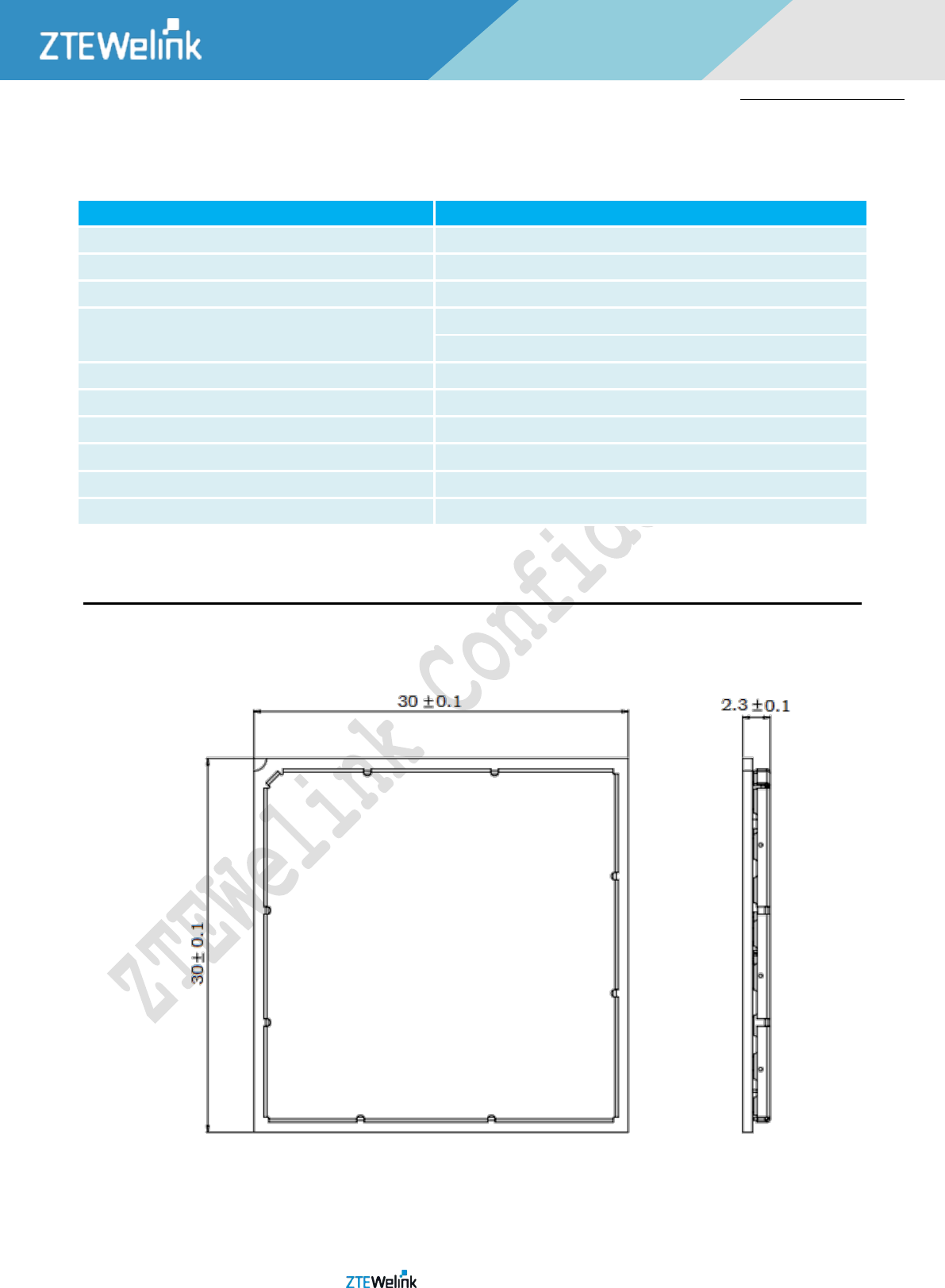
All Rights reserved, No Spreading abroad without Permission 42
ME3631
Hardware Development Guide
4.5. GPS/GNSS TECHNICAL PARAMETERS
The following table shows the GNSS(GPS/GLONASS) techinical parameters of ME3631 module.
Table 4-10 GNSS Technical Parameters
GPS/GNSS (GNSS/GLONASS)
Technical specification
GPS/GNSS Frequency
1575.42±1.023 MHz
Tracking sensitivity
-156dbm
Cold-start sensitivity
-144dbm
TTFF (Open Sky)
Hot start: 4s
Cold start: 32s
Receiver Type
Qualcomm GNSS Gen8C
GNSS L1 Frequency
1575.42MHz
Update rate
2-4 HZ
GNSS (GPS/GLONASS) data format
ZTE Loc API/ZTE auto-negotiation
GNSS (GPS/GLONASS) Current consumption
65mA
GNSS (GPS/GLONASS) antenna
Passive/Active antenna
5. MECHANICAL DIMENSIONS
This chapter describes the mechanical dimensions of the module. All dimensions are measured in mm.
5.1. MECHANICAL DIMENSIONS OF THE MODULE
Figure 5–1 ME3631 Top and Side Dimensions
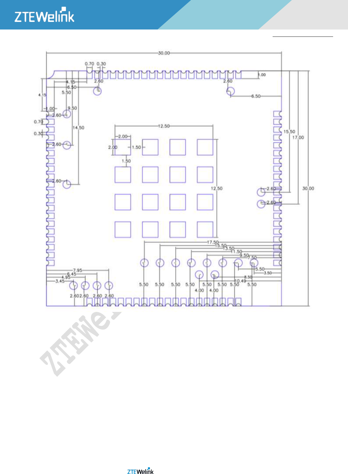
All Rights reserved, No Spreading abroad without Permission 43
ME3631
Hardware Development Guide
Figure 5–2 ME3631 Bottom Dimensions (Bottom view)
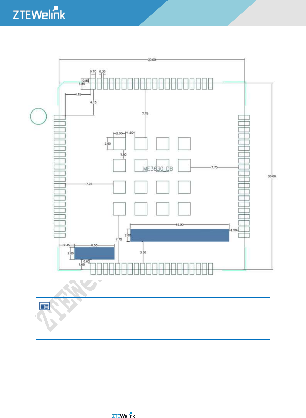
All Rights reserved, No Spreading abroad without Permission 44
ME3631
Hardware Development Guide
5.2. FOOTPRINT OF RECOMMENDATION
Figure 5–3 Recommended Footprint (Top view)
NOTE:
Keep out the area below the test point (circular area on the above figure) in the host PCB.
In order to maintain the module, keep about 3mm between the module and other components in the
host PCB.
5.3. TOP&BOTTOM VIEW OF ME3631
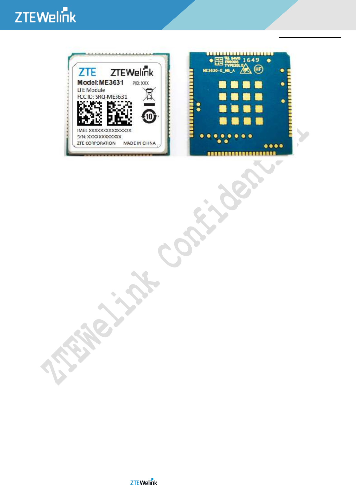
All Rights reserved, No Spreading abroad without Permission 45
ME3631
Hardware Development Guide
Figure 5–4 Top&Bottom View of the ME3631(just for reference)
All Rights reserved, No Spreading abroad without Permission 46
ME3631
Hardware Development Guide
6. RELATED TEST & TEST STANDARD
6.1. TESTING REFERENCE
The related tests of MODULE comply with the IEC standard, including the equipment running under high/low temperature,
storage under high/low temperature, temperature shock and EMC. Table 6-1 is the list of testing standard, which includes the
related testing standards for MODULE.
Table 6-1 Testing Standard
NOTE:
IEC: International Electro technical Commission;
GB/T: Recommended national standard
Test Standard
Document Reference
IEC6006826
Environmental testing-Part2.6: Test FC: Sinusoidal Vibration
IEC60068234
Basic environment testing procedures part2.
IEC60068264
Environmental testing-part2-64: Test FH: vibration, broadband random and guidance.
IEC60068214
Environmental testing-part 2-14: Test N: change of temperature
IEC60068229
Basic environmental testing procedures-part2: Test EB and guidance.
IEC6006822
Environmental testing-part2-2: Test B:dry heat
IEC6006821
Environment testing-part2-1: Test A: cold.
GB/T 15844.2
MS telecommunication RF wireless phone-set environment requirement & experimental method – part 4: Strict level of
experimental condition
GB/T 2423.17
Basic environment experiment of electronic products-Experiment Ka: Salt mist experiment method
GB/T 2423.5
Basic environment experiment of electronic products-Part2: Experiment method Try Ea & Introduction: Shock
GB/T 2423.11
Basic environment experiment of electronic products-Part2: Experiment method Try Fd: Broad frequency band random vibration
(General requirement)
TIA/EIA 603 3.3.5
TIA Standard-part3-5:Shock Stability
All Rights reserved, No Spreading abroad without Permission 47
ME3631
Hardware Development Guide
6.2. DESCRIPTION OF TESTING ENVIRONMENT
The working temperature range of MODULE is divided into the normal working temperature range and the extreme working
temperature range. Under the normal working temperature range, the testing result of RF complies with the requirements of 3GPP
specifications, and its function is normal. Under the extreme temperature range, the RF index basically complies with the 3GPP
specifications, and the quality of data communication is affected to a certain extent, but its normal function is not affected. MODULE
has passed the EMC test. Table 6-2 is the requirement for the testing environment, and Table 6-3 lists out the instruments and
devices that might be used during the test.
WARNING:
Table 6-2 lists the extreme working conditions for the Module. Using the Module beyond these conditions
may result in permanent damage to the module.
Table 6-2 Testing Environment
Working Condition
Min Temperature
Max Temperature
Remark
Normal working condition
-30°C
75°C
All the indexes are good.
Extreme working condition
-40~ -30°C
75~85°C
Some indexes become poorer.
Storage
-40°C
85°C
Storage environment of module
Table 6-3 Testing Instrument & Device
Testing Item
Instrument & Device
RF test
Comprehensive testing device
RF cable
Tower antenna
Microwave darkroom
High/Low-temperature running & storage test
High/Low-temperature experimental box
Temperature shock test
Temperature shock experimental box
Vibration test
Vibration console
All Rights reserved, No Spreading abroad without Permission 48
ME3631
Hardware Development Guide
6.3. RELIABILITY TESTING ENVIRONMENT
The reliability test includes the vibration test, high/low-temperature running, high/low-temperature storage and temperature
shock experiment test. Refer to Table 6-4 for the specific parameters.
Table 6-4 Reliability Features
Test Item
Test Condition
Test Standard
Random vibration
Frequency range: 5-20Hz, PSD: 1.0m2/s3
Frequency range: 20-200Hz, -3dB/oct
3 axis, 1 hour for each axis
IEC 68-2-6
Temperature shock
Low temperature: -40°C ± 2°C
High temperature: +80°C ± 2°C
Temperature changing period: less than 30s
Test duration: 2 hours
Cycle: 10
IEC 68-2-14 Na
High-temperature running
Normal high temperature: 75 °C
Extreme high temperature: 85°C
Duration: 24 hours
ZTE standard
Low-temperature running
Normal low temperature: -30°C
Extreme low temperature: -40°C
Duration: 24 hours
ZTE standard
High temperature & high humidity
Temperature: +60°C
Humidity: 95%
Duration: 48 hours
ZTE standard
High temperature storage
Temperature: 85°C
Duration: 24 hours
IEC 68-2-1 Ab
Low temperature storage
Temperature: -40°C
Duration: 24 hours
IEC 68-2-2 Bb
All Rights reserved, No Spreading abroad without Permission 49
ME3631
Hardware Development Guide
7. SMT PROCESS AND BAKING GUIDE
This chapter describes module’s storage, PAD design, SMT process parameters, baking requirements, etc., and it is applicable
for the process guide to second-level assembly of LCC encapsulation module.
7.1. STORAGE REQUIREMENTS
Storage conditions: temperature<40℃, relative humidity<90% (RH), 12 months weld ability guaranteed under this
circumstances of excellent sealing package.
The Moisture sensitivity level for all modules is level 3 (Conforming to IPC/JEDEC J-STD-020). After opening the package, mount
within 168 hours under the environment conditions of temperature<30℃, relative humidity<60% (RH). If it doesn’t meet the above
requirements, perform the baking process. See the baking parameters in Table below:
Table 7-1 Baking parameters
Temperature
Baking conditions
Baking time
Remarks
125± 5℃
Moisture: ≤60%RH
8 hours
The accumulated baking time must be less than 96 hours
45± 5℃
Moisture: ≤5%RH
192 hours
The product’s transportation, storage and processing must conform to IPC/JEDEC J-STD-033
When in the process of PAD designing of module, refer to IPC-SM-782A and the chapter 6.2 below.
7.2. MODULE PLAINNESS STANDARD
Plainness of the module is required to be less than 0.15mm.
Measurement method: put the module on the marble plane, use the feeler gage to measure the gap width at the position of
maximum warp, and do not exert force on the module during the measurement.
7.3. PROCESS ROUTING SELECTION
The modules are manufactured with the lead-free process and meet the ROHS requirements, therefore it’s recommended to
follow the lead-free manufacturing process upon the selection of process routing for module board and main board.
7.3.1. SOLDER PASTE SELECTION
The solder pastes with metal particle TYPE3 and TYPE4 can fulfill the welding requirements. It is accordingly recommended to
use the no-clean solder paste. If the solder paste which needs cleaning is used, we cannot guarantee the components on the module
board could withstand the washing of the cleaning solvents. This might cause the functional problems of such components and affect
the appearance of the module. During the printing process, make sure the solder paste’s thickness at the position of module’s PAD is
within 0.18mm~0.20mm.
7.3.2. DESIGN OF MODULE PAD’S STEEL MESH OPENING ON MAIN BOARD
The thickness of the steel mesh on main board is selected according to the encapsulation type of components on the main
board. Pay attention to the following requirements:
Make sure to design the module PAD on main board according to chapter 5.
The thickness of steel mesh is 0.15mm or 0.18mm, but the thickness at the position of module pad can be increased to
0.18~0.20mm or the thickness of steel mesh is directly 0.18mm~0.20mm on main board.
Requirements on the thickness of solder paste: control the thickness between 0.18mm and 0.20mm.
See the LCC module PAD’s steel mesh opening in the following table:
Table 7-2 LCC module PAD’s steel mesh opening
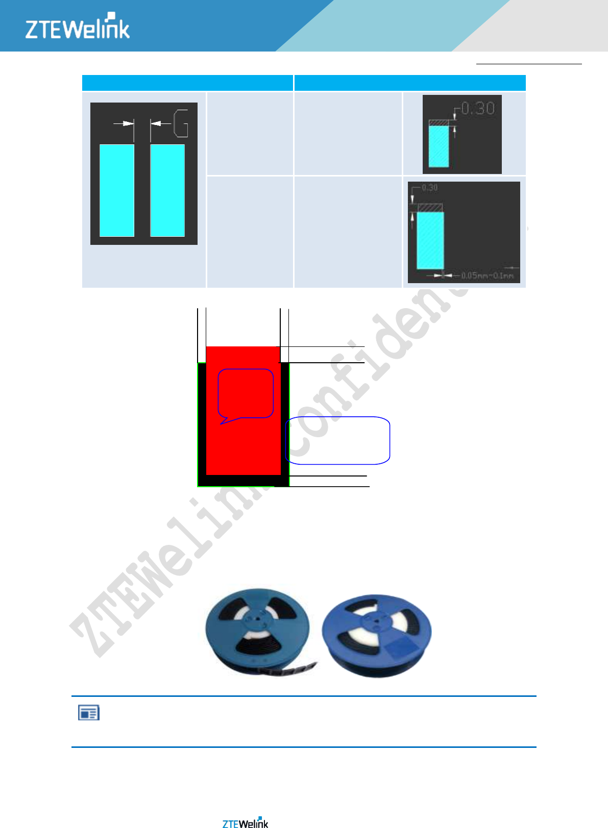
All Rights reserved, No Spreading abroad without Permission 50
ME3631
Hardware Development Guide
Module PAD GAP (G)=Center Distance (e)-PAD width (X)
Steel mesh opening
G≥0.5mm
Drill holes at 100% scale in
the direction of width;
extend 0.3mm outward in
the direction of length
G<0.5mm
Contract 0.05~0.1mm in the
direction of width;
Contract 0.05~0.1mm inward
in the direction of length,
extend 0.5mm outward in
the direction of length.
Figure 7–1 Module Board’s Steel Mesh Diagram
7.3.3. MODULE BOARD’S SMT PROCESS
1) SMT Tape Reel:
The tape reels, which are suitable for SMT, have been made for most ZTE modules. If the module has provided the tape reel
itself and meets the SMT requirements, customers can directly use it for module SMT.
Figure 7–2 Material Module Pallet
NOTE:
Figure7-2 is just for reference, it doesn’t represent the actual Material Module Tape Reel.
Otherwise, customers need make a loading tool similar to the tape reel. Customers can take out the module from the
packaging box, put them into the tape according to the sequence and direction, and then start SMT.
0.1mm
0.1mm
0.5mm
0.1mm
Steel
mesh
opening
Module PAD on PCB
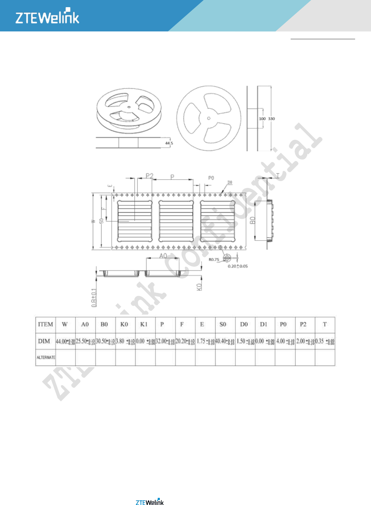
All Rights reserved, No Spreading abroad without Permission 51
ME3631
Hardware Development Guide
2) Tape Reel Dimension (unit: mm):
The following picuture is the tape reel specific dimension for your reference:
A: Whole dimension:
B: Detailed dimension:
Figure 7–3 Tape Reel Dimension
3) Mounting Pressure:
In order to ensure a good contact between the module and the solder paste on main board, the pressure of placing the module
board on main board should be 2-5N according to our experiences. Different modules have different numbers of pads, therefore the
pressure selected are different. Customers can select proper pressure based on their own situations to suppress the module paste as
little as possible, in order to avoid the surface tension of the solder paste melts too much to drag the module during reflow.
7.3.4. MODULE SOLDERING REFLOW CURVE
Module soldering furnace temperature curve is:
Peak value: 245+0/-5℃
≥217℃: 30~~60S
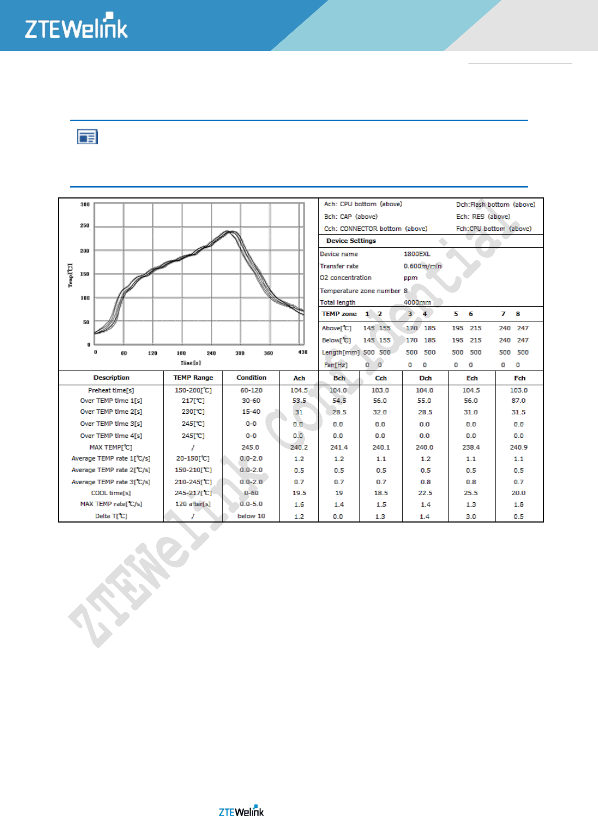
All Rights reserved, No Spreading abroad without Permission 52
ME3631
Hardware Development Guide
150~200℃: 60~~120S
Temperature rise slope: <3℃/S
Temperature drop rate: -2~-4℃/S
NOTE:
The test board of furnace temperature must be the main board with the module board mounted on, and
there must be testing points at the position of module board.
Figure 7–4 Module Furnace Temperature Curve Reference Diagram
7.3.5. REFLOW METHOD
If the main board used by customers is a double-sided board, it is recommended to mount the module board at the second
time. In addition, it is preferable for the main board to reflow on the mesh belt when mounting at the first time and the second time.
If such failure is caused by any special reason, the fixture should be also used to make such main board reflow on the track so as to
avoid the deformation of PCB during the reflow process.
7.3.6. MAINTENANCE OF DEFECTS
If poor welding occurs to the module board and main board, e.g., pseudo soldering of the module board and main board, the
welder can directly use the soldering iron to repair welding according to the factory’s normal welding parameters.
7.4. MODULE’S BAKING REQUIREMENTS
The module must be baked prior to the second reflow.
7.4.1. MODULE’S BAKING ENVIRONMENT
The operators must wear dust-free finger cots and anti-static wrist strap under the lead-free and good static-resistant
All Rights reserved, No Spreading abroad without Permission 53
ME3631
Hardware Development Guide
environment. Refer to the following environment requirements:
WARNING:
The product’s transportation, storage and processing must conform to IPC/JEDEC J-STD-033.
7.4.2. BAKING DEVICE AND OPERATION PROCEDURE
Baking device: Any oven where the temperature can rise up to 125°C or above.
Precautions regarding baking: during the baking process, the modules should be put in the high-temperature resistant pallet
flatly and slightly to avoid the collisions and frictions between the modules. During the baking process, do not overlay the modules
directly because it might cause damage to the module’s chipset.
7.4.3. MODULE BAKING CONDITIONS
See the baking parameters in Table 7-1.
8. FEDERAL COMMUNICATION COMMISSION INTERFERENCE STATEMENT
This device complies with Part 15 of the FCC Rules. Operation is subject to the following two conditions: (1) This
device may not cause harmful interference, and (2) this device must accept any interference received, including
interference that may cause undesired operation.
This equipment has been tested and found to comply with the limits for a Class B digital device, pursuant to Part
15 of the FCC Rules. These limits are designed to provide reasonable protection against harmful interference in a
residential installation. This equipment generates, uses and can radiate radio frequency energy and, if not installed
and used in accordance with the instructions, may cause harmful interference to radio communications. However,
there is no guarantee that interference will not occur in a particular installation. If this equipment does cause harmful
interference to radio or television reception, which can be determined by turning the equipment off and on, the user
is encouraged to try to correct the interference by one of the following measures:
● Reorient or relocate the receiving antenna.
● Increase the separation between the equipment and receiver.
● Connect the equipment into an outlet on a circuit different from that to which the receiver is connected.
● Consult the dealer or an experienced radio/TV technician for help.
FCC Caution:
Any changes or modifications not expressly approved by the party responsible for compliance could void the
user's authority to operate this equipment.
This transmitter must not be co-located or operating in conjunction with any other antenna or transmitter.
Radiation Exposure Statement:
This equipment complies with FCC radiation exposure limits set forth for an uncontrolled environment. This
equipment should be installed and operated with minimum distance 20cm between the radiator & your body.
This device is intended only for OEM integrators under the following conditions:
1) The antenna must be installed such that 20 cm is maintained between the antenna and
users, and the maximum antenna gain allowed for use with this device is 4.8 dBi.
2) The transmitter module may not be co-located with any other transmitter or antenna.

All Rights reserved, No Spreading abroad without Permission 54
ME3631
Hardware Development Guide
As long as 2 conditions above are met, further transmitter test will not be required. However, the OEM
integrator is still responsible for testing their end-product for any additional compliance requirements required
with this module installed
IMPORTANT NOTE: In the event that these conditions can not be met (for example certain laptop
configurations or co-location with another transmitter), then the FCC authorization is no longer considered valid
and the FCC ID can not be used on the final product. In these circumstances, the OEM integrator will be
responsible for re-evaluating the end product (including the transmitter) and obtaining a separate FCC
authorization.
End Product Labeling
This transmitter module is authorized only for use in device where the antenna may be installed such that 20
cm may be maintained between the antenna and users. The final end product must be labeled in a visible area
with the following: “Contains FCC ID:SRQ-ME3631”. The grantee's FCC ID can be used only when all FCC
compliance requirements are met.
Manual Information To the End User
The OEM integrator has to be aware not to provide information to the end user regarding how to install or
remove this RF module in the user’s manual of the end product which integrates this module. The end user
manual shall include all required regulatory information/warning as show in this manual.