ZTE MG2639 GSM/GPRS Module User Manual MG2639 V1 0en 0314
ZTE Corporation GSM/GPRS Module MG2639 V1 0en 0314
UserManual.wiki
>
ZTE
>
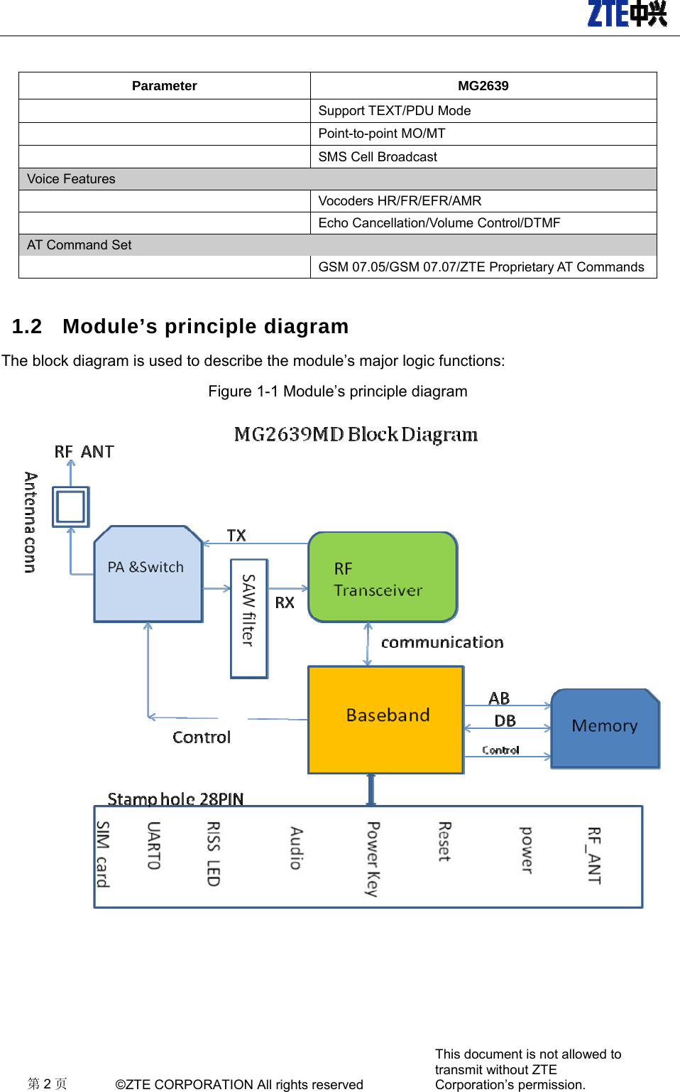
MG2639 User Manual
User Manual
Navigation menu
Upload a User Manual
Namespaces
Wiki Guide
HTML
PDF
Info
Views
User Manual
Discussion / Help
Navigation