ZTE MG2639 GSM/GPRS Module User Manual MG2639 V1 0en 0314
ZTE Corporation GSM/GPRS Module MG2639 V1 0en 0314
ZTE >
User Manual

MG2639 User Manual
Version:V1.0

This document is not allowed to
transmit without ZTE Corporation’s
permission. ©ZTE CORPORATION All rights reserved 第I页
Copyright Statement
Copyright © 2010 by ZTE Corporation
All rights reserved.
No part of this publication may be excerpted, reproduced, translated or utilized in any form or by
any means, electronic or mechanical, including photocopying and microfilm, without the prior
written permission of ZTE Corporation.
is the registered trademark of ZTE Corporation. All other trademarks appeared in
this manual are owned by the relevant companies.
ZTE Corporation reserves the right to make modifications on print errors or update specifications
in this manual without prior notice.
ZTE Corporation keeps the right to make the final explanation to this manual.
第II 页 ©ZTE CORPORATION All rights reserved
This document is not allowed to
transmit without ZTE
Corporation’s permission.
Descriptions of version update
Product version Document version Document No. Descriptions of
document update
MG2639 V1.0
Release for the first
time
Author
Document
version Date Written by Checked by Approved by
1.0 2011-8-22 Zhou Tao

This document is not allowed to
transmit without ZTE Corporation’s
permission. ©ZTE CORPORATION All rights reserved 第III 页
With strong technical force, ZTE Corporation can provide CDMA/GPRS/WCDMA module
customers with the following all-around technical support:
1. Provide complete technical documentation;
2. Provide the development board used for R&D, test, production, after-sales, etc.;
3. Provide evaluations and technical diagnosis for principle diagram, PCB, test scenarios;
4. Provide test environment;
ZTE Corporation provides customers with onsite supports, and also you could get supports
through telephone, website, instant communication, E-mail, etc.

第IV 页 ©ZTE CORPORATION All rights reserved
This document is not allowed to
transmit without ZTE
Corporation’s permission.
Preface
Summary
This document introduces MG2639 module’s product principle diagram, PINs, hardware interface
and module’s mechanical design, which can instruct the users how to quickly and conveniently
design different kinds of wireless terminals based on this type of module.
Target Readers
This document mainly applies to the following engineers:
System designing engineers
Mechanical engineers
Hardware engineers
Software engineers
Test engineers

This document is not allowed to
transmit without ZTE Corporation’s
permission. ©ZTE CORPORATION All rights reserved 第V页
Contents
1GENERAL DESCRIPTION OF MODULE ........................................................................ 1
1.1INTRODUCTION OF MODULE’S FUNCTIONS ..................................................... 1
1.2MODULE’S PRINCIPLE DIAGRAM ....................................................................... 2
1.3ABBREVIATIONS ................................................................................................... 3
2DESCRIPTIONS OF MODULE’S EXTERNAL INTERFACES ........................................ 5
2.1DEFINITIONS OF MODULE’S INTERFACES ........................................................ 5
2.2ANTENNA INTERFACE ......................................................................................... 6
3MODULE’S ELECTRICAL CHARACTERISTICS ........................................................... 8
3.1DESCRIPTIONS OF LEVELS OF INTERFACE SIGNALS ..................................... 8
3.1.1RESET .......................................................................................................... 8
3.1.2SIM CARD INTERFACE ............................................................................... 8
3.1.3AUDIO INTERFACE ..................................................................................... 9
3.1.4NETWORK SIGNAL INDICATION ................................................................ 9
3.2MODULE POWER CONSUMPTION .................................................................... 10
3.3RELIABILITY CHARACTERISTICS ..................................................................... 10
4INTERFACE CIRCUIT DESIGN .................................................................................... 11
4.1RESET AND POWER DESIGN ............................................................................ 11
4.2UART INTERFACE ............................................................................................... 12
4.3SIM CARD INTERFACE ....................................................................................... 13
4.4AUDIO INTERFACE ............................................................................................. 14
5MECHANICAL DIMENSIONS ....................................................................................... 15
5.1APPEARANCE DIAGRAM ................................................................................... 15
5.2MODULE ASSEMBLY DIAGRAM ........................................................................ 15
5.3PCB DIMENSIONS .............................................................................................. 16
6ANTENNA INTERFACE ................................................................................................ 16
6.1ANTENNA INSTALLATION .................................................................................. 17
6.2ANTENNA PAD .................................................................................................... 17
6.3ANTENNA CONNECTOR .................................................................................... 17

第VI 页 ©ZTE CORPORATION All rights reserved
This document is not allowed to
transmit without ZTE
Corporation’s permission.
6.4ANTENNA SUBSYSTEM ..................................................................................... 18
6.4.1ANTENNA SPECIFICATIONS .................................................................... 18
6.4.2CABLE LOSS.............................................................................................. 19
6.4.3ANTENNA GAIN MAXIMUM REQUIREMENTS ......................................... 19
6.4.4ANTENNA MATCHING ............................................................................... 19
6.4.5PCB DESIGN CONSIDERATIONS ............................................................. 19
ANTENNA INTERFACE ................................................................................................. 19
7OEM/INTEGRATORS INSTALLATIONS ...................................................................... 20

This document is not allowed to
transmit without ZTE Corporation’s
permission. ©ZTE CORPORATION All rights reserved 第VII 页
Figures
Figure 1-1 Module’s principle diagram ............................................................................................ 2
Figure 2-1 Antenna interface diagram ............................................................................................. 6
Figure 5-1 MG2639 module’s appearance .................................................................................... 15
Figure 5-2 Module’s assembly diagram ........................................................................................ 15
Figure 5-3 Relevant PCB dimensions ........................................................................................... 16
Tables
Table 1-1 Module’s functions .......................................................................................................... 1
Table 1-1 28Pin stamp-hole definition............................................................................................. 5
Table 4-1 Voltage characteristics .................................................................................................. 11
This document is not allowed to
transmit without ZTE Corporation’s
permission. ©ZTE CORPORATION All rights reserved 第1页
1 General description of module
This chapter mainly provides a general description of the module, including basic functions and
logic block diagram.
1.1 Introduction of module’s functions
The maximum operating ambient temperature of the equipment declared by the manufacturer is
75℃
Table 1-1 Module’s functions
Parameter MG2639
General Features
Frequency Bands GSM850/EGSM900/DCS1800/PCS1900
Dimensions 30.0×25.0x2.68mm
Weight 7g
Operating Temperature Range -30°C~+75°C
Storage Temperature Range -40°C~+85°C
Performance
Operating Voltage Range 3.6V~4.2V/Typical: 3.9V
Current Consumption Typically
Idle Current: 2mA
Call Current: 128mA
Max Current: 300mA
TX Power GSM850/EGSM900: Class 4 (2W)
DCS1800/PCS1900: Class 1 (1W)
RX Sensitivity <-106dBm
Interfaces
Connector 28Pin Stamp Holes
Antenna SMT 50Ω Antenna Connector
Antenna Solder Pad
Integrated Full Duplex UART AT/Data
SIM Card Interface 1.8V/3.0V
Data Features
GPRS Class 10
Mobile Station Class B
Max Downlink 85.6kbps
Max Uplink 42.8kbps
Protocol Internal TCP/IP&UDP
Embedded FTP
SMS Features
第2页 ©ZTE CORPORATION All rights reserved
This document is not allowed to
transmit without ZTE
Corporation’s permission.
Parameter MG2639
Support TEXT/PDU Mode
Point-to-point MO/MT
SMS Cell Broadcast
Voice Features
Vocoders HR/FR/EFR/AMR
Echo Cancellation/Volume Control/DTMF
AT Command Set
GSM 07.05/GSM 07.07/ZTE Proprietary AT Commands
1.2 Module’s principle diagram
The block diagram is used to describe the module’s major logic functions:
Figure 1-1 Module’s principle diagram
This document is not allowed to
transmit without ZTE Corporation’s
permission. ©ZTE CORPORATION All rights reserved 第3页
1.3 Abbreviations
A
ADC Analog-Digital Converter
AFC Automatic Frequency Control
AGC Automatic Gain Control
ARFCN Absolute Radio Frequency Channel Number
ARP Antenna Reference Point
ASIC Application Specific Integrated Circuit
B
BER Bit Error Rate
BTS Base Transceiver Station
C
CDMA Code Division Multiple Access
CDG CDMA Development Group
CS Coding Scheme
CSD Circuit Switched Data
CPU Central Processing Unit
D
DAI Digital Audio interface
DAC Digital-to-Analog Converter
DCE Data Communication Equipment
DSP Digital Signal Processor
DTE Data Terminal Equipment
DTMF Dual Tone Multi-Frequency
DTR Data Terminal Ready
E
EDGE Enhanced Data Rate for GSM Evolution
EFR Enhanced Full Rate
EGSM Enhanced GSM
EMC Electromagnetic Compatibility
EMI Electro Magnetic Interference
ESD Electronic Static Discharge
ETS European Telecommunication Standard
F
FDMA Frequency Division Multiple Access
FR Full Rate
G
GPRS General Packet Radio Service
GSM Global Standard for Mobile Communications
H
HR Half Rate
I
IC Integrated Circuit
IMEI International Mobile Equipment Identity
ISO International Standards Organization
ITU International Telecommunications Union
L
第4页 ©ZTE CORPORATION All rights reserved
This document is not allowed to
transmit without ZTE
Corporation’s permission.
LCD Liquid Crystal Display
LED Light Emitting Diode
M
MCU Machine Control Unit
MMI Man Machine Interface
MS Mobile Station
MTBF Mean Time Before Failure
P
PCB Printed Circuit Board
PCL Power Control Level
PCS Personal Communication System
PDU Protocol Data Unit
PLL Phase Locked Loop
PPP Point-to-point protocol
R
RAM Random Access Memory
RF Radio Frequency
ROM Read-only Memory
RMS Root Mean Square
RTC Real Time Clock
S
SIM Subscriber Identification Module
SMS Short Message Service
SMT Surface Mount Technology
SRAM Static Random Access Memory
T
TA Terminal adapter
TDMA Time Division Multiple Access
TE Terminal Equipment also referred it as DTE
U
UART Universal asynchronous receiver-transmitter
UIM User Identifier Management
USB Universal Serial Bus
USIM Universal Subscriber Identity Module
V
VSWR Voltage Standing Wave Ratio
Z
ZTE ZTE Corporation
This document is not allowed to
transmit without ZTE Corporation’s
permission. ©ZTE CORPORATION All rights reserved 第5页
2 Descriptions of module’s external interfaces
This chapter mainly describes the module’s external interfaces, such as B2B connector, MINI
PCI-E, stamp-hole connector, etc.
2.1 Definitions of module’s interfaces
Table 1-1 28Pin stamp-hole definition
No. Definition I/O Description Remarks
1 GND GND
2 RF_ANT I/O RF antenna
3 GND GND
4 RING O Ring signal
indication
Level varies upon an incoming call or
receipt of text message.
5 GND GND
6 VBAT I Work voltage
7 RSSI_LED O Network signal
indication
Internal pull-down, LED on at high
level, need add triode driver
externally.
-power-on status: LED off;
-network searching status: LED
blinks at 3Hz
-Idle status: LED blinks at 1Hz
-Traffic status (call, data): LED blinks
at 5Hz.
8 RTS I Request to send
第6页 ©ZTE CORPORATION All rights reserved
This document is not allowed to
transmit without ZTE
Corporation’s permission.
9 CTS O Clear to send
10 DCD O Carrier detection
11 CARD_RST O card reset
12 CARD_CLK O card clock
13 CARD_DATA I/O card data
14 V_CARD O Card voltage
15 RXD I Receive data
16 TXD O Transmit data
17 SYSRST_N I Reset signal Valid at low level, need connect an
open collector/drain switch.
18 SPK_2P O Headset Speaker +
19 SPK_1P O Microphone
speaker +
20 SPK_1N O Microphone
speaker -
21 MIC_2P I Headset
microphone +
22 MIC_1P I Receiver
microphone +
23 MIC_1N I Receiver
microphone -
24 PWRKEY_N I power on-off Valid at low level, need connect an
open collector/drain switch.
25 DTR I Data terminal ready
_WAKEUP
26 DSR O Data set ready
27 V_MSM O 2.8V
28 GND GND
2.2 Antenna interface
MG2639 module provides two kinds of antenna interface:
PCB welding pad
Antenna test socket
PCB welding pad adopts 50Ω RF shield cable to connect the module and the antenna, in order to
reduce the cost. However, using this method can’t completely shield the electromagnets, which
might have slight influence on RF signal quality. Please note that there should not be strong
radiation near the welding pad. Meantime, during the welding, make sure the core of RF shield
cable must connect with RF welding pad, and RF shield cable’s shield metal mask must be welded
to the module’s GND. During the welding, the GND must be welding securely, otherwise the core is
easily broken due to the shaking of shield cable. See figure 2-1 for RF welding pad antenna.
Figure 2-1 Antenna interface diagram
This document is not allowed to
transmit without ZTE Corporation’s
permission. ©ZTE CORPORATION All rights reserved 第7页
第8页 ©ZTE CORPORATION All rights reserved
This document is not allowed to
transmit without ZTE
Corporation’s permission.
3 Module’s electrical characteristics
This chapter mainly introduces the module’s electrical characteristics, including the level, power
consumption, reliability of module’s interfaces.
3.1 Descriptions of levels of interface signals
It describes the MAX, MIN and typical value of the level of module’s external interfaces.
3.1.1 Reset
SYSRST_N PIN is used to reset the module’s main chip, and SYSRST_N signal needs to be
pulled down 500ms to reset the module. Likewise, this pin is required to pull up 2.8V (Max: 2.9V,
Min: 2.7V, typical: 2.8V) through 4.7K resistor inside the module, and pull down 0.1uF capacitance
to GMD filtering, and it’s required to externally connect dynatron driver.
MG2639 module provides 1CH serial interface, supports 8-wire serial BUS interface or 4-wire
serial BUS interface or 2-wire serial interface. The module communicates with the external devices
and inputs AT commands through UART interface.
Classification Definition I/O Description Min.
voltage Typical
voltage Max.
voltage
UART RXD I Receive data 2.4V 2.8V 3.1V
/RTS I Request to send 2.4V 2.8V 3.1V
TXD O Transmit data 2.4V 2.8V 3.1V
/DTR I Data terminal
ready_WAKEUP
2.4V 2.8V 3.1V
/CTS O Clear to send 2.4V 2.8V 3.1V
RING O Ring signal
indication
2.4V 2.8V 3.1V
/DSR O Data set ready 2.4V 2.8V 3.1V
DCD O Carrier detection 2.4V 2.8V 3.1V
3.1.2 SIM Card Interface
MG2639 module baseband processor integrates SIM card interface conforming to ISO 7816-3
standard, and it’s compatible with SIM card with two voltages 1.8V/3.0V and reserves SIM card
interface signal on the stamp-hole PIN.
Users should note that SIM card’s electrical interface definitions are the same as SIM card socket’s
definitions.
Figure 3-1 Standard SIM card PIN Definitions Diagram
This document is not allowed to
transmit without ZTE Corporation’s
permission. ©ZTE CORPORATION All rights reserved 第9页
Classification Definition I/O Description Remarks
SIM V_CARD O Card voltage 1.8V/3V; maximum
output current 20mA
CARD_RST O Card reset
GND GND
CARD_CLK O Card clock
CARD_DATA I/O Card data
3.1.3 Audio Interface
MG2639 module supports 2CH audio signal inputs/outputs. It features in handheld microphone,
handheld receiver or hands-free speaker and earpiece microphone/receiver function. These two
MIC inputs are coupled in AC domain and the offset voltage is added inside, and they should
directly connect with the receiver. The two receiver interfaces SPK_1 and SPK_2 are both
differential interfaces with 32Ωresistance; SPK_2 is single-ended interface with 32Ω resistance.
See the audio interface signals in the table below:
Classification Definition I/O Description Remarks
AUDIO MIC_1N I Receiver’s Microphone- The first differential receiver
used for the default audio
input/output and the second
receiver used for headset
audio input/output.
MIC_1P I Receiver’s Microphone+
MIC_2P I Headset microphone +
SPK_1N O Receiver’s speaker-
SPK_1P O Receiver’s speaker+
SPK_2P O Headset speaker +
3.1.4 Network Signal Indication
RSSI_LED Internal pull-down, LED turns on at high level, and need add triode driver externally.
-Power-on status: LED off;
-Network searching status: LED blinks at 3Hz
-Idle status: LED blinks at 1Hz
-Traffic status (call, data): LED blinks at 5Hz.
第10 页 ©ZTE CORPORATION All rights reserved
This document is not allowed to
transmit without ZTE
Corporation’s permission.
SIG_LED PIN output status is defined according to the software protocol, and users could judge
the module’s work status according to SIG_LED status. SIG_LED PIN is common I/O port, which
can’t directly drive LED, and it needs to work with dynatron.
3.2 Module Power Consumption
It describes the module’s power consumption under each status:
No. Test items
Typical value(mA)
1 Power-off leakage current
(Normal power-off)
50uA
2 Average standby current (no
operation after power-on)
2mA
3 Average standby current (after
talk)
2mA
4 Talk current 128mA
3.3 Reliability Characteristics
It describes the temperature, including working temperature and storage temperature.
Working temperature: -30°C~+75°C
Storage temperature: -40°C~+85°C
This document is not allowed to
transmit without ZTE Corporation’s
permission. ©ZTE CORPORATION All rights reserved 第11 页
4 Interface circuit design
It provides the reference design circuit of the interface and precautions according to the module’s
functions.
4.1 Reset and power design
See the reference design principle of power and reset circuit in figure 4-1:
Figure 4-1 Power and reset circuit reference design principle diagram
Power design
MG2639 module is powered by VBAT. See the voltage characteristics in table 4-1.
Table 4-1 Voltage characteristics
Classification MIN Typical MAX
Input voltage 3.4V 3.9V 4.25V
Input current 2mA(average)-- 300mA(depends on the
network signal)
D1 is an enabled LDO with 6V~9V input voltage. Through adjusting R31and R41, it could make
V_MAIN at 3.9V to power the module, and it’s required to place at least one 1000uF tantalum
capacitor at V-Main input pin. The module is very strict with the requirements on power and GND,
therefore it’s requested that filtering must be performed to power and GND, and the power ripple
must be controlled under 50Mv. Do not use LDO to power any other part in the system because it
might affect the RF performance. Finally, select the power cables with at least 80mil traces during
the layout and keep the integrality of ground line.
If MG2639 module uses other LDO, make sure the output current is larger than 2A.
Power on
The module is under power-off status after it’s normally powered on. To turn on the module,
provide a 2s-5s low level pulse to PWRKEY_N pin when the module is OFF. If one 1K resistance is
connected with PWRKEY_N, the module can be turned on after power supply.
Note: ON/OFF and /Reset need to connect an open collector/drain gate.
It’s not required to operate /RESET signal upon power-on.
第12 页 ©ZTE CORPORATION All rights reserved
This document is not allowed to
transmit without ZTE
Corporation’s permission.
Power off
To turn off the module, use AT command “AT+ZPWROFF” or provide a 2s~5s low level pulse to
PWRKEY_N PIN.
Reset
Use the above method to firstly “power-off” and then “power-on” to hard reset the module.
If the external reset function has to be used, low level pulse lasting at least 500ms should be
provided to /RESET Pin within 2 seconds after the module is turned on. Before that, the external
I/O signal must be kept at low level. See the reset circuit design in figure 4-1.
If SYSRST_N Pin is not used, suspend the pin.
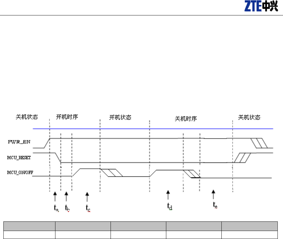
See the module’s power-on/off time sequence in the diagram below:
Figure 4-1 Power-on/off time sequence
Table 4-2 Power-on/off circuit time characteristics
ta tb tc td te
20ms 10ms 3s 3s 6s
V_MSM
There is a voltage output pin with current adjuster, which can be used to supply external power to
the board. The voltage of this pin and the voltage of baseband processor/memory come from the
same voltage adjuster. The voltage output is available only when the module is on. The normal
output voltage is 2.85V, and the user should absorb the current from this pin as little as possible
(less than 10mA). Generally, it is recommended to use this pin to match the level.
When the module is off, the output voltage for this pin remains unchanged, but the impedance is
rather high. Therefore, it’s not recommended to use this pin for other purposes.
Other advice
In order to make sure the data is saved safely, please don’t cut off the power when the module is
on. It’s strongly recommended to add battery or soft switch like the power key on the module.
4.2 UART interface
Note: when using the module for overall design, the users should export UART for module’s
software upgrade.
MG2639 module provides an integrated full duplex UART interface and an accessorial full duplex
UART interface, whose maximal data rate is 115200bps. External interface is 2.8VCMOS level
signal, their logic functions conform to RS-232 interface standard. These two UART could be used
as serial port data interfaces, usually UART1 is used for AT commands, data transmission and
updating software of module.
The module’s output IO level is 2.8V,it needs to transfer the level when connecting with standard
3.3V or 5V logic circuit(such as MCU or RS232 drive chip MAX3238 etc), Figure 4-3 shows the
COM port level transfer circuit. The converted signal should connect with MCU or RS232 drive chip
This document is not allowed to
transmit without ZTE Corporation’s
permission. ©ZTE CORPORATION All rights reserved 第13 页
directly. Common low power switch triode should be applied as the crystal triode shown in Figure
4-3. Please note that the module won’t enter sleep mode as RXD is at high level.
Figure 4-3 UART interface reference design block diagram
Remarks: the module doesn’t support USB.
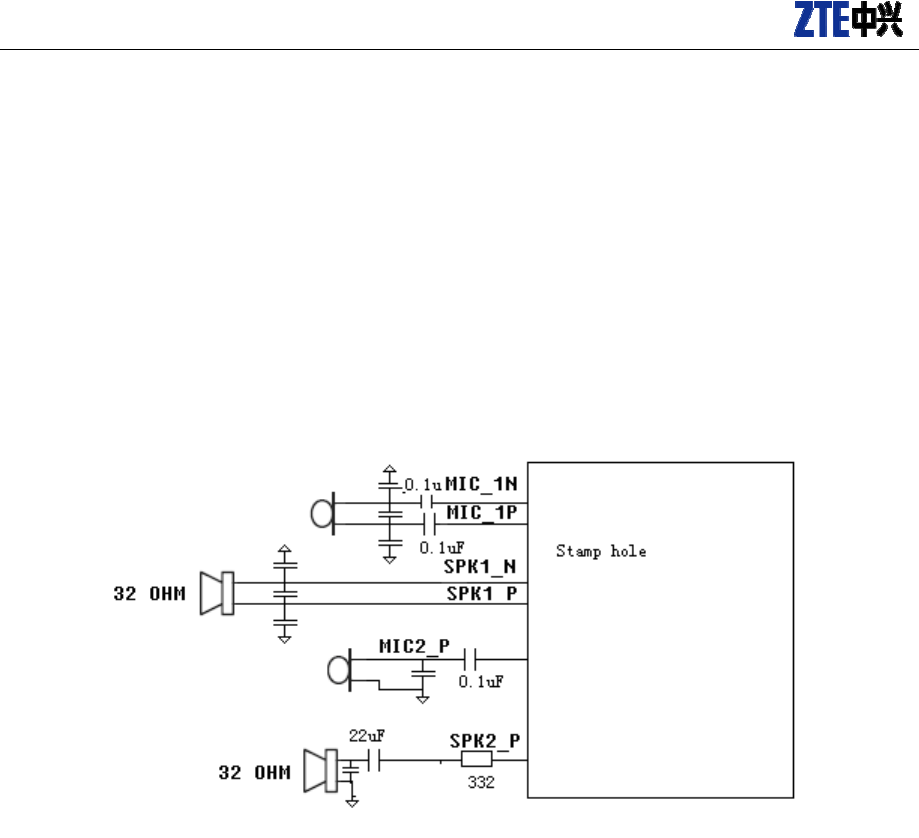
4.3 SIM card interface
MG2639 module supports 1.8V or 3V SIM card, and there are 4 pins at the terminal of the
card. V_CARD is used to supply SIM card. It’s strongly recommended to add ESD to
protect SIM card in hostile environments.
Figure 4-4 SIM card circuit reference design diagram
第14 页 ©ZTE CORPORATION All rights reserved
This document is not allowed to
transmit without ZTE
Corporation’s permission.
NOTE: The SIM card PCB wiring should be laid closely around the module as much as possible to
prevent the interference sources from affecting the SIM card’s reading/writing. Besides, Since the
SIM card needs to be designed to meet the requirements of ESD performance and avoid the
damage of the SIM card caused by ESD, it’s recommended to add TVS components on 4-CH SIM
card signals, meanwhile, the signal wires need go through TVS component before entering the
module’s baseband processor during the layout.
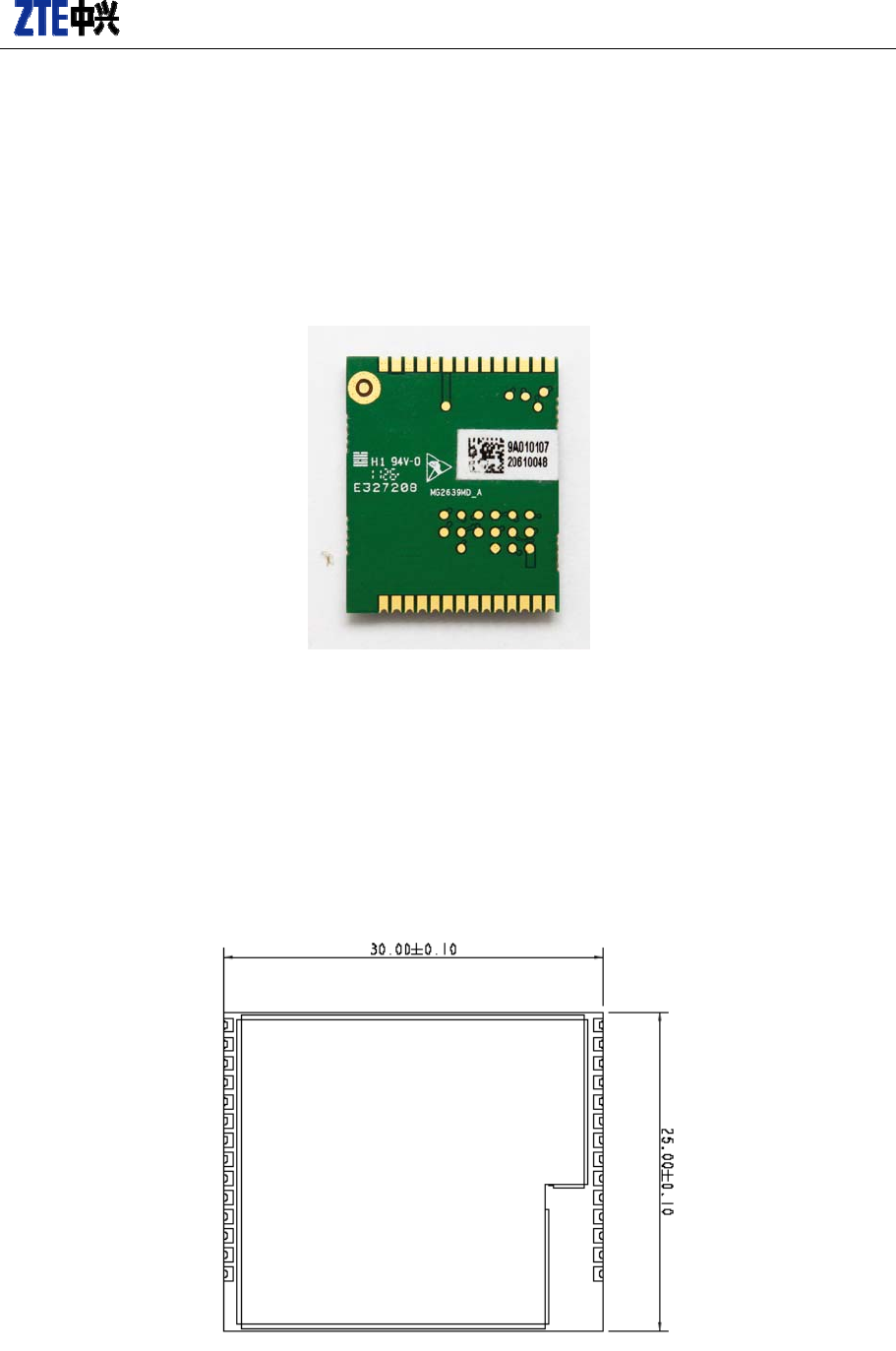
4.4 Audio interface
MG2639 module provides audio input and output interfaces through its PINs. There are 2
Speaker interfaces and 2 Microphone interfaces. Only one pair I/O works at the same time. See
the audio interface circuit in figure 4-5.
Figure 4-5 Audio interface circuit reference design principle diagram
Microphone
The system connector provides two microphone interfaces MIC_1 and MIC_2, MIC_1 is differential
interface; while MIC_2 is single ended interface. These two inputs are coupled in AC domain and
2.0V offset voltage are added inside, therefore they should directly connect to the microphone.
Speaker
The system connector provides two speakers, SPK_1 & SPK_2. SPK_1 is differential interface,
while SPK_2 is single-ended interface. They both have 32 ohm impedance.
GSM/GPRS module audio interface is designed as below:
Design of the audio interface on the receiver
Select the microphone with the sensitivity lower than -51.5dB since the output impedance for
SPK_1 is 32 ohm and the max. gain in MIC_1 reaches 51.5dB. The level of MIC_1P PIN is about
2.2V.
Note: if other kind of audio input method is adopted, the input signal should be within 0.5V. If the
signal voltage is lower than 0.5V, then the pre-amplifier should be added. If the signal voltage is
higher than 0.5V, then network attenuation should be added.
Design of the audio interface on the headset
Select the microphone with the sensitivity lower than -51.5dB since the output impedance for
SPK_2 is 32 ohm and the max. gain in MIC_2 reaches 51.5dB. The level of MIC_2P PIN is about
2.2V. The design is just the same as that on the receiver
This document is not allowed to
transmit without ZTE Corporation’s
permission. ©ZTE CORPORATION All rights reserved 第15 页
5 Mechanical dimensions
It introduces the module’s mechanical dimensions.
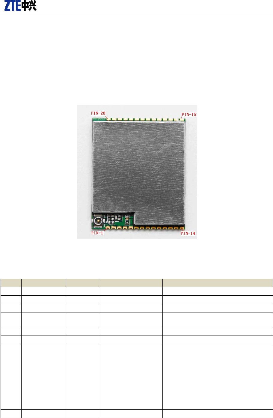
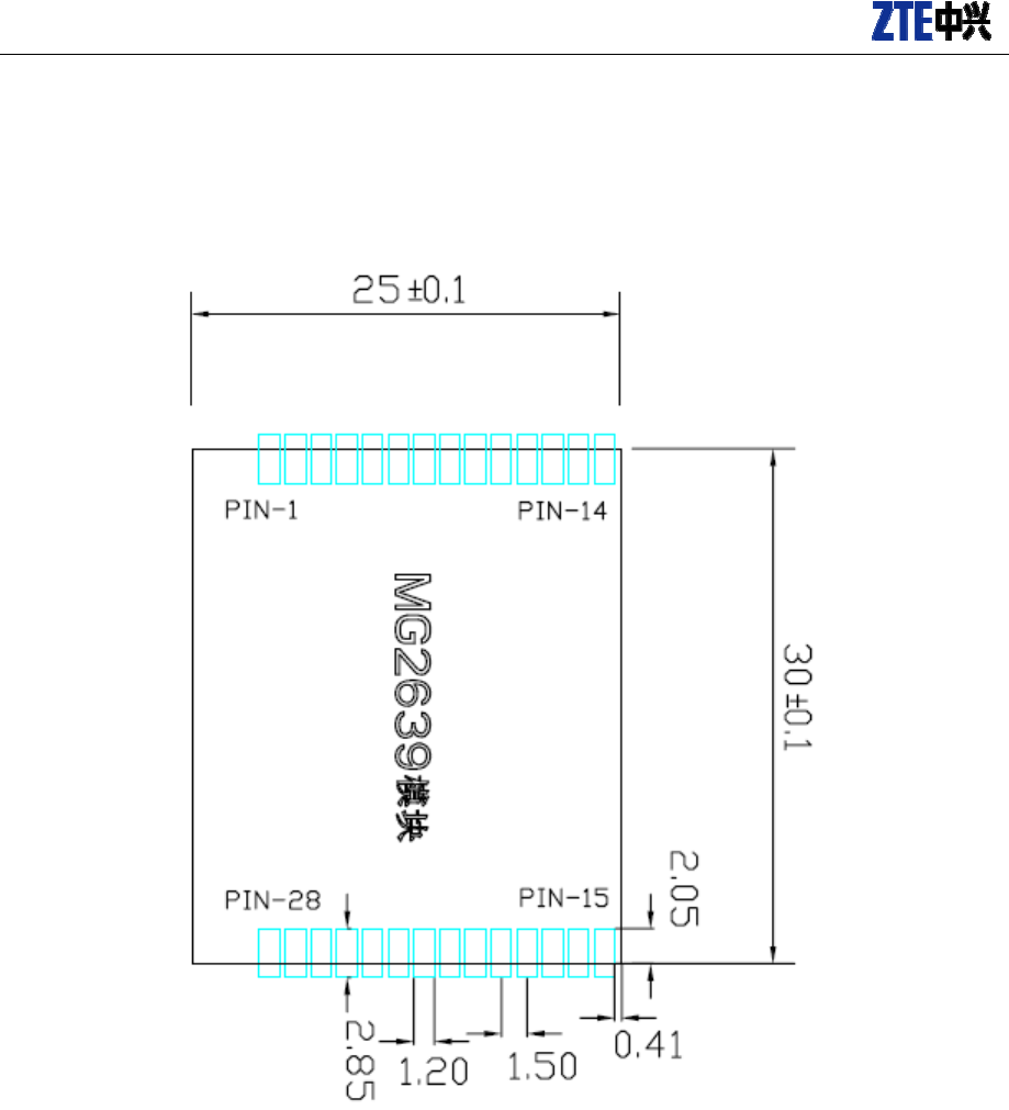
5.1 Appearance Diagram
Figure 5-1 MG2639 module’s appearance
Dimensions(L×W×H):30.0×25.0×2.68mm
Weight:7g
5.2 Module Assembly Diagram
See the module assembly diagram in figure 5.2.
Figure 5-2 Module’s assembly diagram
第16 页 ©ZTE CORPORATION All rights reserved
This document is not allowed to
transmit without ZTE
Corporation’s permission.
5.3 PCB Dimensions
See the module’s PCB dimensions in figure 5-3.
Figure 5-3 Relevant PCB dimensions
Precautions while designing PCB:
1)Copper-clad and wiring are forbidden at the area below the RF test points.
2)For the convenience of testing and maintenance, it might be necessary to drill holes on the PCB.
6 Antenna Interface
The RF interface of the MG2639 Module has an impedance of 50 . The module is capable of sustaining a
total mismatch at the antenna connector or pad without any damage, even when transmitting at maximum
RF power.
The external antenna must be matched properly to achieve best performance regarding radiated power,
DC-power consumption, modulation accuracy and harmonic suppression. Antenna matching networks are
not included on the MG2639 Module PCB and should be placed in the host application.
This document is not allowed to
transmit without ZTE Corporation’s
permission. ©ZTE CORPORATION All rights reserved 第17 页
Regarding the return loss, the Module provides the following values in the active band:
Table 6-1 Return Loss in the Active Band
State of Module Return Loss of
Module Recommended Return Loss of
Application
Receive ≥ 8dB ≥ 12dB
Transmit not applicable ≥ 12dB
The connection of the antenna or other equipment must be de coupled from DC voltage. This is necessary
because the antenna connector is DC coupled to ground via an inductor for ESD protection.
6.1 Antenna Installation
To suit the physical design of individual applications, the MC2261 offers two alternative approached to
connecting the antenna:
■ Recommended approach: MM9329-2700B antenna connector manufactured by MURATA assembled on
the component side of the PCB (top view on Module). See Section 4.3 for details.
■ Antenna pad and grounding plane placed on the bottom side. See Section 4.2 for details.
The MM9329-2700B connector has been chosen as antenna reference point (ARP) for the ZTEMT
reference equipment submitted to type approve the MG2639 Module. All RF data specified throughout this
manual are related to the ARP. For compliance with the test results of the ZTEMT type approval you are
advised to give priority to the connector, rather than using the antenna pad.
Note: Both solutions can be applied alternatively. This means,if the antenna is connected to the pad, then
the connector on the Module must be left empty,and when the antenna is connected to the Module
connector, the pad is useless,
6.2 Antenna Pad
The antenna pad of the module is soldered to the board on the customer design to connect with RF line.
For proper grounding connect the RF line to the ground plane on the bottom of the MG2639 Module which
must be connected to the ground plane of the application.
Consider that according to GSM recommendations as 50Ω connector is mandatory for type approval
measurements. It must be ensured that the RF line which is connected to antenna pad should be controlled
on 50Ω.
Notes on soldering
■ To prevent damage to the Module and to obtain long-term solder joint properties, you are advised to
maintain the standards of good engineering practice for soldering.
Material Properties
■ MG2639 Module PCB: FR4
■ Antenna pad: Gold plated pad
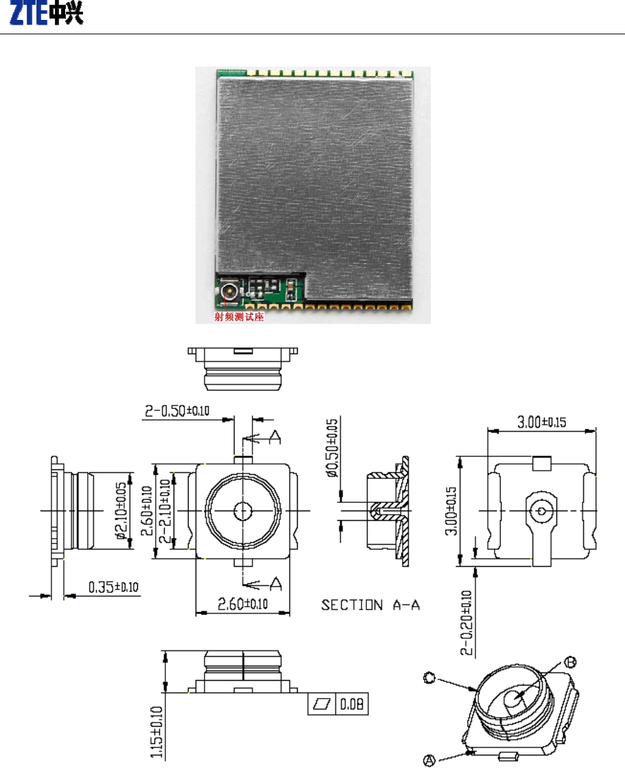
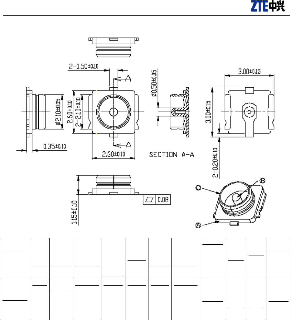
6.3 Antenna connector
The MG2639 Module uses a microwave coaxial connector supplied by Murata Ltd. The product name is
MM9329-2700B. The position of the antenna connector on the Module PCB can be seen in Figure 6-3.
Figure 6-3 Specification of MM9329-2700B connector
第18 页 ©ZTE CORPORATION All rights reserved
This document is not allowed to
transmit without ZTE
Corporation’s permission.
Table 6-2 Product specifications of MM9329-2700B connector
Part
Number
Rated
Volta
g
e (V)
Contact
Resista
n
ce
(ohm)
Withstand
i
ng
Voltage
(rms)
Insulati
o
n
Resistan
ce (M
ohm)
Durabil
i
ty
(cycles)
Freque
n
cy
Rating
(GHz)
Temperat
u
re
Range
(degree C)
VSWR Cente
r
Conta
ct
Outer
Conta
ct
Insulato
r
MM932
9
-2700B
250 0.015
max.
300 (AC) 500 min. 100 DC - 6.0 -40~+90. 1.2 max.
(DC~3G
H
z)
Coppe
r
Alloy
Gold
plated
Coppe
r
Alloy
Silver
plated
Engineer
i
ng
plastic
6.4 Antenna Subsystem
The antenna sub-system and its design is a major part of the final product integration. Special attention and
care should be taken in adhering to the following guidelines.
6.4.1 Antenna Specifications
Choice of the antenna cable (type, length, performance, RF loss, etc) and antenna connector (type + losses)
can have a major impact on the success of the design.

This document is not allowed to
transmit without ZTE Corporation’s
permission. ©ZTE CORPORATION All rights reserved 第19 页
6.4.2 Cable Loss
All cables have RF losses. Minimizing the length of the cable between the antenna and the RF connectors
on the module will help obtain superior performance. High Quality/Low loss co-axial cables should be used
to connect the antenna to the RF connectors. Contact the antenna vendor for the specific type of cable that
interfaces with their antenna and ask them to detail the RF losses of the cables supplied along with the
antenna. Typically, the cable length should be such that they have no more than 1-2dB of loss. Though the
system will work with longer (lossy) cables, this will degrade GSM system performance. Care should also
be taken to ensure that the cable end
connectors/terminations are well assembled to minimize losses and to offer a reliable, sturdy connection to
the Module sub-system. This is particularly important for applications where the module is mounted on a
mobile or portable environment where it is subject to shock and vibration.
6.4.3 Antenna Gain Maximum Requirements
Our FCC Grant imposes a maximum gain for the antenna subsystem: 2 dBi for the GSM850 band and 2dBi
for the 1900 band.
Warning: Excessive gain could damage sensitive RF circuits and void the warranty.
6.4.4 Antenna Matching
The module’s RF connectors are designed to work with a 50-ohm subsystem. It is assumed that the antenna
chosen has matching internal to it to match between the 50-ohm RF connectors and the antenna impedance.
6.4.5 PCB Design Considerations
• The antenna subsystem should be treated like any other RF system or component. It should be isolated as
much as possible from any noise generating circuitry including the interface signals via filtering and
shielding.
• As a general recommendation all components or chips operating at high frequencies such as
micro controllers, memory, DC/DC converts and other RF components should not be placed too close to the
module. When such cases exist, correct supply and ground de-coupling areas should be designed and
validated.
• Avoid placing the components around the RF connection and close to the RF line between the RF antenna
and the module.
• RF lines and cables should be as short as possible.
• If using coaxial cable it should not be placed close to devices operating at low frequencies. Signals like
charger circuits may require some EMI/RFI decoupling such as filter capacitors or ferrite beads.
• Adding external impedance matching to improve the match to your cable and antenna assemblies is
optional. Please contact the antenna vendor for matching requirements.
• For better ESD protection one can implement a shock coil to ground and place it close to the RF
connector.
Antenna Interface
Proper measures should be taken to reduce the access loss of effective bands, and good shielding should be
established between the external antenna and the RF connector. Besides, the external RF cables should be
kept far away from all interference sources such as high-speed digital signal or switch power supply.
According to mobile station standard, stationary wave ratio of antenna should be between1.1 to 1.5, and
input impedance is 50 ohm. Different environments may have different requirements on the antenna’s gain.
Generally, the larger gain in the band and smaller outside the band, the better performance the antenna has.
Isolation degree among ports must more than 30dB when multi-ports antenna is used. For example, between

第20 页 ©ZTE CORPORATION All rights reserved
This document is not allowed to
transmit without ZTE
Corporation’s permission.
two different polarized ports on dual-polarized antenna, two different frequency ports on dual-frequency
antenna, or among four ports on dual-polarized dual-frequency antenna, isolation degree should be more
than 30dB.
7 OEM/Integrators Installations
Clear and specific instructions describing the conditions, limitations and procedures for third-parties to use
integrate the module into a host device.
Important compliance information for North American users
The MG2639 Module has been granted modular approval for mobile applications. Integrators may use the
MG2639 Module in their final products without additional FCC certification if they meet the following
conditions. Otherwise, additional FCC approvals must be obtained.
1. At least 20cm separation distance between the antenna and the user’s body must be maintained at all
times.
2. To comply with FCC regulations limiting both maximum RF output power and human exposure to RF
radiation, the maximum antenna gain including cable loss in a mobile-only exposure condition must not
exceed 2dBi in the cellular band and 2dBi in the PCS band.
3. The MG2639 Module and its antenna must not be co-located or operating in conjunction with any other
transmitter or antenna within a host device.
4. A label must be affixed to the outside of the end product into which the MG2639 Module is
incorporated, with a statement similar to the following:·ForMG2639: This device contains FCC ID:
Q78-MG2639.
5. A user manual with the end product must clearly indicate the operating requirements and conditions
that must be observed to ensure compliance with current FCC RF exposure guidelines.
The end product with an embedded MG2639 Module may also need to pass the FCC Part 15 unintentional
emission testing requirements and be properly authorized per FCC Part 15.
Note: If this module is intended for use in a portable device, you are responsible for separate
approval to satisfy the SAR requirements of FCC Part 2.1093.

This document is not allowed to
transmit without ZTE Corporation’s
permission. ©ZTE CORPORATION All rights reserved 第21 页
8. EU Regulatory Conformance
Hereby, ZTE CORPORATION declares that this device is in compliance with the essential requirements
and other relevant provisions of Directive 1999/5/EC.
For the declaration of conformity, visit the Web site www.zte.com