Users Manual

Hardware Development Guide of
Module Product
Version V1.0, 2015-09-28
MW3650

Hardware Development Guide of Module Products
All Rights reserved, No Spreading abroad without Permission of ZTEWelink II
MW3650
0
Legal Information
By receiving the document from Shenzhen ZTEWelink Technology Co., Ltd (shortly referred to as
ZTEWelink), you are deemed to have agreed to the following terms. If you don’t agree to the
following terms, please stop using the document.
Copyright © 2015 Shenzhen ZTEWelink Technology Co., Ltd. All rights reserved. The document
contains ZTEWelink’s proprietary information. Without the prior written permission of
ZTEWelink, no entity or individual is allowed to reproduce, transfer, distribute, use and disclose
this document or any image, table, data or other information contained in this document.
is the registered trademark of ZTEWelink. The name and logo of ZTEWelink are
ZTEWelink’s trademark or registered trademark. Meanwhile, ZTEWelink is granted to use ZTE
Corporation’s registered trademark. The other products or company names mentioned in this
document are the trademark or registered trademark of their respective owner. Without the prior
written permission of ZTEWelink or the third-party oblige, no one is allowed to read this
document.
The product meets the design requirements of environmental protection and personal security. The
storage, use or disposal of products should abide by the product manual, relevant contract or the
laws and regulations of relevant country.
ZTEWelink reserves the right to make modifications on the product described in this document
without prior notice, and keeps the right to revise or retrieve the document any time.
If you have any question about the manual, please consult the company or its distributors promptly.
Hardware Development Guide of Module Products
All Rights reserved, No Spreading abroad without Permission of ZTEWelink III
MW3650
0
Revision History
Version Date Description
1.0 2015-09-28 1
st
released version

Hardware Development Guide of Module Products
All Rights reserved, No Spreading abroad without Permission of ZTEWelink IV
MW3650
0
Contents
Figures ................................................................................................................................................. VII
Tables ................................................................................................................................................. VIII
1 About This Document .................................................................................................................. 10
1.1 Application Range ......................................................................................................... 10
1.2 Purpose .......................................................................................................................... 10
1.3 Supported & Reference Documents List ....................................................................... 11
1.4 Abbreviations ................................................................................................................ 11
2 Product Overview ......................................................................................................................... 13
2.1 Technical Parameters ..................................................................................................... 14
2.2 Function Overview ........................................................................................................ 16
2.2.1 Baseband Function ................................................................................................ 16
2.2.2 Radio Frequency Function .................................................................................... 16
3 Mechanic Features ....................................................................................................................... 18
3.1 Module Illustration ........................................................................................................ 18
3.2 Module hex-vision images ............................................................................................ 19
3.3 Module Main Board PCB Encapsulation Dimension Diagram ..................................... 19
3.4 PCB Design Guidelines ................................................................................................. 21
3.5 Suggestions for Heat-dissipation Design ....................................................................... 22
4 Interfaces....................................................................................................................................... 23
4.1 Definition of PINs ......................................................................................................... 23
4.2 Hardware interface description ...................................................................................... 27
4.3 Ground ........................................................................................................................... 28
4.4 Power Interface .............................................................................................................. 28
4.4.1 V_MAIN PINS ..................................................................................................... 28
4.4.2 VREF PINS ........................................................................................................... 30
4.4.3 Power interface PCB Layout and Wiring Guidance .............................................. 30
4.5 Power-on/Power-off & Reset......................................................................................... 31
4.5.1 Power On .............................................................................................................. 31

Hardware Development Guide of Module Products
All Rights reserved, No Spreading abroad without Permission of ZTEWelink V
MW3650
0
4.5.2 Power Off .............................................................................................................. 31
4.5.3 Reset ...................................................................................................................... 32
4.5.4 Power-on/Power-off Flow ..................................................................................... 32
4.6 UART Interface ............................................................................................................. 34
4.7 (U)SIM Card Interface .................................................................................................. 36
4.8 USB Interface ................................................................................................................ 38
4.9 Working Status Indicator Interface ................................................................................ 39
4.10 SPI Bus Interface ........................................................................................................... 40
4.11 I2C Bus .......................................................................................................................... 41
4.12 User Interface ................................................................................................................ 42
5 Antenna ......................................................................................................................................... 43
5.1 Preliminary Antenna Evaluation .................................................................................... 43
5.2 Antenna Design Guidance ............................................................................................. 43
5.3 Suggested Antenna Location ......................................................................................... 44
5.4 RF PCB wire guidelines ................................................................................................ 45
5.5 EMC Requirements ....................................................................................................... 45
5.6 Index Requirement of Antenna ...................................................................................... 46
5.6.1 Passive Index of Antenna ...................................................................................... 46
5.6.2 Active Index of Antenna ....................................................................................... 47
5.6.3 OTA Test method of Whole Machine Antenna ...................................................... 48
6 Electric Feature ............................................................................................................................ 49
6.1 Interface PWL ............................................................................................................... 49
6.2 Power Supply ................................................................................................................ 49
6.3 Working Current ............................................................................................................ 49
7 Technical Index of Radio Frequency .......................................................................................... 51
7.1 Index of RF under UMTS Mode ................................................................................... 51
7.1.1 Maximum Transmission Power ............................................................................. 51
7.1.2 Receiving Sensibility ............................................................................................ 52
7.1.3 Spurious Emission Index ....................................................................................... 52
7.2 Index of RF under GPRS/GSM/EDGE Mode ............................................................... 52
7.2.1 Maximum Transmission Power ............................................................................. 53
7.2.2 Receiving Sensibility ............................................................................................ 53

Hardware Development Guide of Module Products
All Rights reserved, No Spreading abroad without Permission of ZTEWelink VI
MW3650
0
7.2.3 Spurious Emission Index ....................................................................................... 53
8 Related Test & Test Standard ...................................................................................................... 55
8.1 Testing Reference .......................................................................................................... 55
8.2 Description of Testing Environment .............................................................................. 56
8.3 Reliability Testing Environment .................................................................................... 56
8.4 Reliability Testing Result .............................................................................................. 57
8.5 ESD Characteristic ........................................................................................................ 58
9 SMT Process and Baking Guide ................................................................................................. 59
9.1 Storage Requirements .................................................................................................... 59
9.2 Module’s Position Requirements on Main board .......................................................... 59
9.3 Module Planeness Standard ........................................................................................... 60
9.3.1 Process Routing Selection ..................................................................................... 60
9.3.2 Solder Paste Selection ........................................................................................... 60
9.3.3 Design of module PAD’s steel mesh opening on main board................................ 61
9.3.4 Module Board’s SMT process ............................................................................... 62
9.3.5 Module Soldering Reflow Curve .......................................................................... 63
9.3.6 Reflow method ...................................................................................................... 64
9.3.7 Maintenance of defects ......................................................................................... 64
9.4 Module’s Baking Requirements .................................................................................... 64
9.4.1 Module’s Baking Environment ............................................................................. 64
9.4.2 Baking device and operation procedure ................................................................ 65
9.4.3 Module Baking Conditions ................................................................................... 65
10 Safety Warnings and Notes .......................................................................................................... 66

Hardware Development Guide of Module Products
All Rights reserved, No Spreading abroad without Permission of ZTEWelink VII
MW3650
0
Figures
Figure 2-1 System Connection Structure ............................................................................. 16
Figure 4-1 PIN Configuration Diagram ............................................................................... 23
Figure 4-2 Wakeup Waveform .............................................................................................. 26
Figure 4-3 LDO Power Supply ............................................................................................ 29
Figure 4-4 DC/DC Switching Power Supply ....................................................................... 30
Figure 4-5 Power On & Reseting Circuit Reference Diagram ............................................. 31
Figure 4-6 Power-on Sequence Chart of Module ................................................................. 33
Figure 4-7 Power-off Sequence Chart of Module ................................................................ 33
Figure 4-8 UART Interface PWL Conversion Reference Design ........................................ 35
Figure 4-9 Module Serial Port & AP Application Processor ............................................... 35
Figure 4-10 The Connection of UART and Standard RS-232-C Interface .......................... 36
Figure 4-11 (U)SIM Card Console Circuit Reference Design ............................................. 37
Figure 4-12 USB Interface Circuit Reference Design Schematic Diagram ......................... 39
Figure 5-1 Translation Circuit Diagram ............................................................................... 44
Figure 5-2 OTA Test System ............................................................................................... 48
Figure 9-1 Green oil and white oil at module’s position on main board .............................. 60
Figure 9-2 Module Board’s Steel Mesh Diagram ................................................................ 62
Figure 9-3 Material Module Pallet ....................................................................................... 62
Figure 9-4 Module Furnace Temperature Curve Diagram ................................................... 63

Hardware Development Guide of Module Products
All Rights reserved, No Spreading abroad without Permission of ZTEWelink VIII
MW3650
0
Tables
Table 1-1 Support Documents List ...................................................................................... 11
Table 1-2 Abbreviation List ................................................................................................. 11
Table 2-1 Module Frequency band configuration ................................................................ 13
Table 2-2 Major Technical Parameters ................................................................................ 14
Table 2-3 Working Frequency Band .................................................................................... 17
Table 3-1 Product Illustration .............................................................................................. 18
Table 4-1 PIN Interface Definition ...................................................................................... 23
Table 4-2 Voltage Current Characteristic ............................................................................ 29
Table 4-3 Power-on/Power-off Time ................................................................................... 33
Table 4-4 The Definition of UART Signal .......................................................................... 34
Table 4-5 The Definition of USIM Card Interface............................................................... 36
Table 4-6 The Definition of USB PINS ............................................................................... 38
Table 4-7 The Correspondence of Port Map ........................................................................ 39
Table 4-8 Indicator Light Reference Design Schematic Diagram ....................................... 40
Table 4-9 The Description of Working Status Indicator Light ............................................ 40
Table 4-10 The Definition of SPI Interface ......................................................................... 40
Table 4-11 I2C Reference Circuit Design ............................................................................ 41
Table 5-1 The Passive Index Reference of Main Antenna about PAD product ................... 46
Table 5-2 The Passive Index Reference of Diversity Antenna about PAD product ............ 46
Table 5-3 Recommended Product OTA Index Requirement ............................................... 47
Table 6-1 Main Out ward Interface PWL of Module ........................................................... 49
Table 6-2 Input Voltage ....................................................................................................... 49
Table 6-3 The Current Consumption under Sleep Mode ..................................................... 50
Table 6-4 The Working Current of MODULE .................................................................... 50
Table 7-1 Maximum Transmission Power ........................................................................... 51
Table 7-2 Reference of Receiving Sensitivity ...................................................................... 52
Table 7-3 Spurious Emission Index ..................................................................................... 52
Table 7-4 Maximum Transmission Power of GSM850/900/1800/1900 (GMSK/8PSK) .... 53
Table 7-5 Receiving Sensitivity ........................................................................................... 53
Table 8-1 Testing Standard .................................................................................................. 55
Table 8-2 Testing Environment ........................................................................................... 56
Table 8-3 Testing Instrument & Device ............................................................................... 56
Table 8-4 Reliability Features .............................................................................................. 56
Table 8-5 The Temperature Testing Result Under Windless Condition .............................. 57
Table 8-6 The High/low Temperature Running and Storage Testing Result ....................... 57
Table 8-7 Module ESD Features .......................................................................................... 58
Table 9-1 Baking parameters ............................................................................................... 59
Table 9-2 LCC module PAD’s steel mesh opening ............................................................. 61
Hardware Development Guide of Module Products
All Rights reserved, No Spreading abroad without Permission of ZTEWelink IX
MW3650
0
R&TTE Regulation:
In all cases assessment of the final product must be mass against the Essential requirements of
the R&TTE Directive Articles 3.1(a) and (b), safety and EMC respectively, as well as any relevant
Article 3.2 requirements.
Hereby, ZTE CORPORATION declares that this product is in complies with the essential
requirements of Article 3 of the R&TTE 1999/5/EC Directive.

Hardware Development Guide of Module Products
All Rights reserved, No Spreading abroad without Permission of ZTEWelink 10
MW3650
0
1
About This Document
1.1 Application Range
This document is applicable as the hardware development guide of MW3650 module produce. Users need to design
products according to the requirement and guide of this document. This document only can be applied to the hardware
application development of MW3650 module product.
1.2 Purpose
This document provides the hardware solutions and development fundamentals for a product with the module. By
reading this document, the user can have an overall knowledge of the module and a clear understanding of the
technical parameters. With this document, the user can successfully fulfill the application and development of 3G
wireless Internet product or equipment.
Besides the product function features and technical parameters, this document also provides the product reliability
tests and related testing standards, business function realization process, RF performance indexes and a guide on the
design of user circuits, to provide the user with a complete design reference.
NOTE:
At present, our company has a large number of module products. Users may come across many module board
welding problems when using the module. To ensure the module board welding first pass yield and guarantee the
module manufacturing and welding quality in the following integration process, please do as the chapter 9 of
Manufacturing Guide in this document.

Hardware Development Guide of Module Products
All Rights reserved, No Spreading abroad without Permission of ZTEWelink 11
MW3650
0
1.3 Supported & Reference Documents List
Besides this hardware development guide, we also provide the Datasheet document, software development guide and
AT command reference guide. Table 1-1 is the support document list.
Table 1-1 Support Documents List
Document NO. Document Name
1 ZTEWelink Software Development Guide of Module
Product(MG3732_V2A&MW3650).pdf
2 ZTEWelink MW3650 Datasheet.pdf
3 AT Command reference guide for ZTEWelink
MG3732_V2A,MW3650 Module.pdf
1.4 Abbreviations
Table 1-2 is a list of abbreviations involved in this document, as well as the English full names.
Table 1-2 Abbreviation List
Abbreviations Full Name
ADC Analog-Digital Converter
ARP Antenna Reference Point
BER Bit Error Rate
BTS Base Transceiver Station
CDMA Code Division Multiple Access
CS Coding Scheme
CSD Circuit Switched Data
CPU Central Processing Unit
DAC Digital-to-Analog Converter
DCE Data Communication Equipment
DSP Digital Signal Processor
DTE Data Terminal Equipment
DTMF Dual Tone Multi-Frequency
DTR Data Terminal Ready
EGSM Enhanced GSM
EMC Electromagnetic Compatibility

Hardware Development Guide of Module Products
All Rights reserved, No Spreading abroad without Permission of ZTEWelink 12
MW3650
0
Abbreviations Full Name
EMI Electro Magnetic Interference
ESD Electronic Static Discharge
ETS European Telecommunication Standard
FDMA Frequency Division Multiple Access
FR Full Rate
GPRS General Packet Radio Service
GSM Global Standard for Mobile Communications
IC Integrated Circuit
IMEI International Mobile Equipment Identity
ISO International Standards Organization
ITU International Telecommunications Union
LCD Liquid Crystal Display
LED Light Emitting Diode
MCU Machine Control Unit
PCB Printed Circuit Board
PCL Power Control Level
PCS Personal Communication System
PDU Protocol Data Unit
PPP Point-to-point protocol
RAM Random Access Memory
RF Radio Frequency
ROM Read-only Memory
RTC Real Time Clock
SIM Subscriber Identification Module
SMS Short Message Service
SPI Serial Peripheral Interface
TE Terminal Equipment also referred it as DTE
UART Universal asynchronous receiver-transmitter
UIM User Identifier Management
USB Universal Serial Bus
UMTS Universal Mobile Telecommunication System
WCDMA Wideband Code Division Multi Access
Hardware Development Guide of Module Products
All Rights reserved, No Spreading abroad without Permission of ZTEWelink 13
MW3650
0
2
Product Overview
MW3650 is a WCDMA/HSDPA/GSM/GPRS/EDGE industry module developed by our company, and it is a wireless
Internet module with LCC interface. The module has voice(optional), short message and data service functions. The
downlink peak data rate is 3.6Mbps and the uplink peak data rate is 384Kbps, so it can supply the users with
economical high speed internet access business, wireless data business and so on. It is widely applied to but not
limited to the various products and equipment such as modem, embedded module, wireless phone, multimedia phone
and touch screen communication device, PAD, vehicle-mounted terminals and electric consumed devices, using the
MW3650 module.
The function features of this module are described as bellow:
1) Support UMTS/HSDPA 850(900)/1900/2100MHz frequency band,
GSM/GPRS/EDGE 850/900/
1800/1900MHz frequency band.
2)
Can supply GSM/GPRS/EDGE and UMTS/HSDPA high speed data access service in a mobile
environment.
3)
Support SMS and voice functions.
4)
Supply (U)SIM card interface (3.0V/1.8V), USB2.0 interface, 8-wire UART (compatible with
2-wire UART), power on/off, reset and so on.
Taking MW3650 module as an example, this document introduces the logical structure, hardware interfaces and main
function in detail. It also supplies the corresponding design reference of hardware and structure.
NOTE:
At present, the frequency band of MW3650 module in UMTS mode can take proper tailoring or configuration
according to the corresponding requirement of customers as is shown blow.
Table 2-1 Module Frequency band configuration
Configuration GSM Bands WCDMA Bands
MW3650V1A 850/1900MHz 1900/850MHz
MW3650V1B 900/1800MHz 2100/900MHz
MW3650V1C 900/1800MHz 2100MHz

Hardware Development Guide of Module Products
All Rights reserved, No Spreading abroad without Permission of ZTEWelink 14
MW3650
0
2.1 Technical Parameters
The major features of the module can be described from the aspects of mechanic feature, base band, radio frequency,
technical standard, environment features and so on. Table below is a list of the major technical parameters and
features supported by module.
Table 2-2 Major Technical Parameters
Type Item Specifications
Mechanical
Feature
Dimensions (L × W × H) 30.0mm × 30..0mm × 2.3mm
Weight About 5g
Encapsulation type LCC with 80 pins
Baseband
(U)SIM/SIM Standard SIM card interface
3V SIM card and 1.8V SIM card
USB interface USB 2.0 HIGH SPEED
UART interface 8-wire UART
Max Power Dissipation
About 2.2W
Power Supply DC 3.3~4.2V, typical value is 3.8V
Working Current
2
Peak current About 0.6A
The average
current in
normal working
About 540mA@UMTS 2100
About 239mA@GSM 900
Standby current About 5mA@UMTS
About 5mA@GSM
RF
GSM Frequency Band EDGE/GPRS/GSM:1900/1800/900/850MHz
UMTS Frequency Band HSDPA/WCDMA:2100/1900/850(900)MHz;
Diversity Reception
Frequency Band NA
1
Max. Transmitter Power
UMTS2100/1900/900/850: Power Class 3 (+24dBm
+2.5/-1.5dBm)
GSM/GPRS 850MHz/900MHz: Power Class 4 (+33dBm +
2.5/-0.5 dBm)
GSM/GPRS 1800MHz/1900MHz: Power Class 1 (+30dBm
+2.5/-0.5 dBm)
EDGE 850MHz/900MHz: Power Class E2 (+27dBm
+4.5/-1.5dBm)
EDGE 1800MHz/1900MHz: Power Class E2 (+26dBm
+4.5/-2.5dBm)

Hardware Development Guide of Module Products
All Rights reserved, No Spreading abroad without Permission of ZTEWelink 15
MW3650
0
Type Item Specifications
Receiving sensitivity
WCDMA2100 : ≤-108dBm
WCDMA1900 : ≤-109dBm
WCDMA900 : ≤-109dBm
WCDMA850 : ≤-109 dBm
GSM850/900/1800/1900 : ≤-107dBm
Main Antenna External, Provide Antenna PAD
Technical
Standard
Data Rate
GSM CS: UL 9.6kbps/DL 9.6kbps
GPRS: Multi-slot Class 10
EDGE: Multi-slot Class 12
WCDMA CS: UL 64kbps/DL 64kbps
WCDMA PS: UL 384kbps/DL 384kbps
HSDPA HSDPA: DL 3.6Mb/s(Category 6)
Protocol HSDPA/WCDMA/EDGE/GPRS/GSM
3GPP Protocol R5, R4, R99
OS
Windows XP (SP2 and later)
Windows Vista & 7
WinCE
Linux
Android
Environmen
t Feature
3
Working Temperature -30 ~ 75° C
Storage Temperature -40 ~ 85° C
Humidity 5%~ 95%
Application
DATA Support
SMS
Support ultra-long SMS
Support Text and PDU mode
Point to point MO and MT
Voice Support
MMS Support (Not support built-in MMS protocol stack
temporarily)
TCP/IP Support
UDP/IP Support
Phonebook Support
Upgrade Support
Hardware Development Guide of Module Products
All Rights reserved, No Spreading abroad without Permission of ZTEWelink 16
MW3650
0
NOTE:
“NA” indicates nonsupport.
Working current value is the average value tested under the max transmitter power. The value may be different in
different condition and environment. Please take the actual measurement as the reference.
Please make sure that the module is started up in the recommended working current range and working
temperature to avoid the damage or the abnormal working of the module.
2.2 Function Overview
2.2.1 Baseband Function
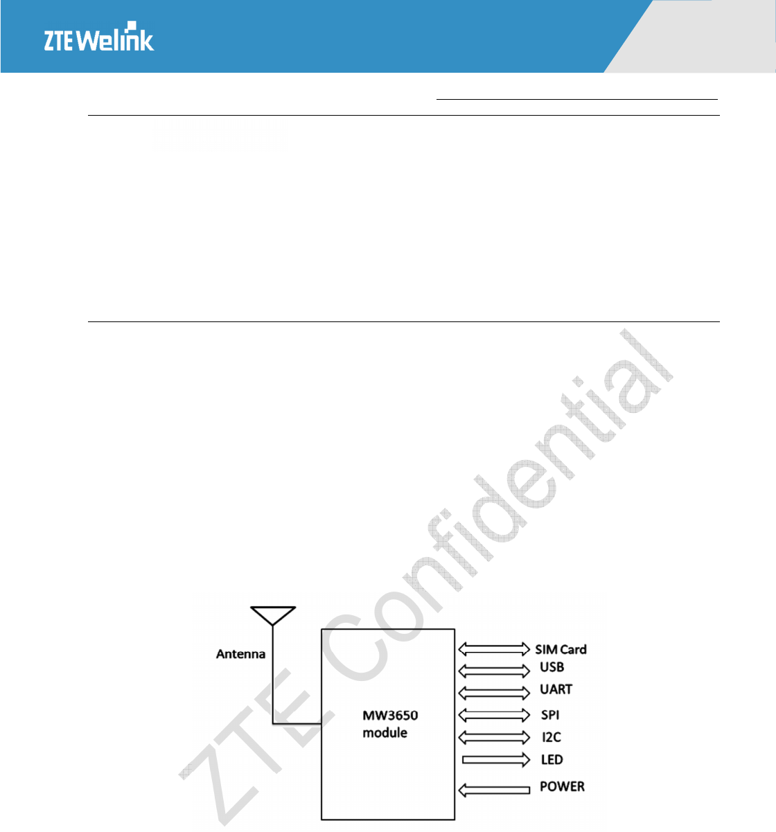
When connected with the system board, the module mainly includes the following signal groups: USB signal, (U)SIM
card signal, status querying signal, UART signal, module power-on/resetting signal, main antenna interface and
power-supply interface. Figure below is the system connection structure.
Figure 2-1 System Connection Structure
2.2.2 Radio Frequency Function
The working frequency band of module is shown in the table below.
a) Support HSDPA/WCDMA 850(900)/1900/2100MHz.
Hardware Development Guide of Module Products
All Rights reserved, No Spreading abroad without Permission of ZTEWelink 17
MW3650
0
b) Support GSM/EDGE/GPRS 850/900/1800/1900MHz.
c) The highest downlink rate supported by HSDPA is 3.6Mbit/s.
d) PS domain supports EDGE CLASS12/GPRS CLASS10 bearer service.
e) CS domain supports 64Kbit/s data service in WCDMA mode.
Table 2-3 Working Frequency Band
Working Frequency Band Uplink Frequency Band Downlink Frequency Band
UMTS850 (band V) 824 MHz — 849 MHz 869 MHz — 894 MHz
UMTS900 (band VIII) 880 MHz — 915 MHz 925 MHz — 960 MHz
UMTS1900 (band II) 1850 MHz — 1910 MHz 1930 MHz — 1990 MHz
UMTS2100 (band I) 1920 MHz — 1980 MHz 2110 MHz — 2170 MHz
GSM850 824 MHz — 849MHz 869 MHz — 894 MHz
GSM900 890 MHz — 915MHz 925 MHz — 960MHz
GSM1800 1710 MHz — 1785MHz 1805 MHz — 1880MHz
GSM1900 1850 MHz — 1910MHz 1930 MHz — 1990MHz
Hardware Development Guide of Module Products
All Rights reserved, No Spreading abroad without Permission of ZTEWelink 18
MW3650
0
3
Mechanic Features
3.1 Module Illustration
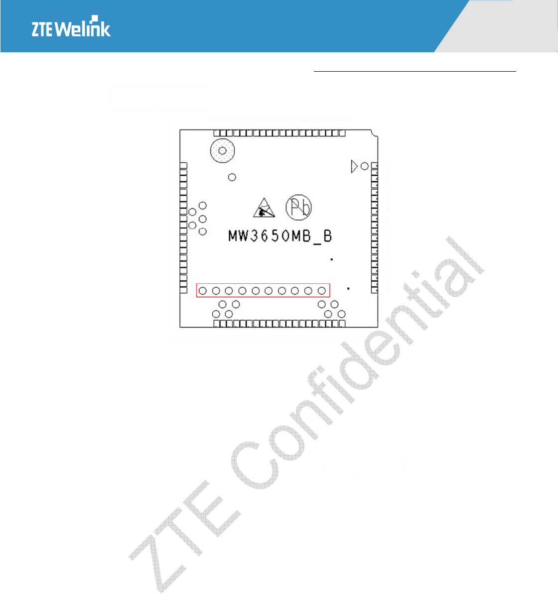
The Product Illustration of module is shown in the Figure 3-1.
Table 3-1 Product Illustration
NOTE:
The picture above is just for reference; please take the actual products as the reference.
Dimensions (L × W × H): 30.0 mm × 30.0mm ×2.3mm
Weight: about 5g
.
Hardware Development Guide of Module Products
All Rights reserved, No Spreading abroad without Permission of ZTEWelink 19
MW3650
0
3.2 Module hex-vision images
The module hex-vision images are shown in figure 3-2 (units: mm).
Figure 3-2 module hex-vision images
Note: the height in the figure above is without the module label, so it is 2.2mm.
3.3 Module Main Board PCB Encapsulation
Dimension Diagram
The detailed dimension of PCB welding panel is shown in figure 3-3 (units: mm).
Hardware Development Guide of Module Products
All Rights reserved, No Spreading abroad without Permission of ZTEWelink 20
MW3650
0
Figure 3-3 The detailed dimension of PCB welding panel
Figure 3-4 Recommended Welding Panel Design Dimension of Customer Interface Board
Hardware Development Guide of Module Products
All Rights reserved, No Spreading abroad without Permission of ZTEWelink 21
MW3650
0
Figure 3-5 PCB Bottom Welding Panel
3.4 PCB Design Guidelines
To ensure the module has good performance in the application process, the users of modules should do
as the following guidelines in the process of PCB wire designing:
1) For testing and maintenance convenience, the customer dev board PCB should be hollowed out to
show the test pionts as is shown in the red box in figure 3-5 so as to do JTAG installation and
debugging.
2) The rest round test points are used for module power supply and calibration in SMT production
process. Do not short out these test points when connect the module to main board.
3) In the design process, the strongly disturbing signals such as clock signal, high-frequency digital
signal and switching signal of switch power supply should be placed far away from the module.
4) Please pay attention to the protection of RF and audio analog signal. If condition permits, it is
better to separate the analog ground and digital ground. After the separation, the signal line or
power line should not pass over the separation channel.
5) To ensure the integrity and circulation ability, if condition permits, it is better to adopt planar form.
6) Please ensure the integrity of the module ground to reduce the leak of disturbing signal.

Hardware Development Guide of Module Products
All Rights reserved, No Spreading abroad without Permission of ZTEWelink 22
MW3650
0
3.5 Suggestions for Heat-dissipation Design
The module will dissipate heat during the working process, and might also be affected by other
high-temperature devices. When do the heat-dissipation design, please pay attention to the following items:
1) Place this product far away from the switch power supply and high speed signal line, and protect the
wiring of these interference sources.
2) Place the antenna and coaxial-cable connecting the network card and antenna far away from these
interference sources.
3) Place the module far away from the devices that have high calorific power such as CPU and
Southbridge to avoid the influencing the RF performance because of the temperature rise.
Hardware Development Guide of Module Products
All Rights reserved, No Spreading abroad without Permission of ZTEWelink 23
MW3650
0
4
Interfaces
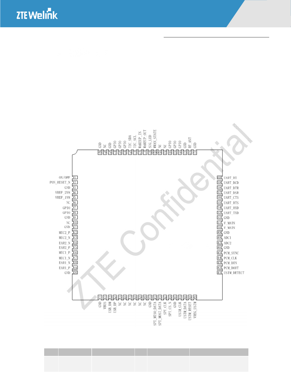
4.1 Definition of PINs
The definition of interface PINs on module is shown in figure 4-1.
Figure 4-1 PIN Configuration Diagram
Table 4-1 PIN Interface Definition
PIN Classification Signal Definition I/O Description Remark
1 POWER_ON ON/OFF I Power on/off Pull-up internally, low
pulse active

Hardware Development Guide of Module Products
All Rights reserved, No Spreading abroad without Permission of ZTEWelink 24
MW3650
0
PIN Classification Signal Definition I/O Description Remark
2 RESET PON_RESET_N I Reset signal 1.8V low level active
3
GND -- GND --
4
VREF_2V8 O Voltage output 2.85V
5
VREF_1V8 O Voltage output 1.8V
6 NC -- -- --
7 GPIO I/O GPIO --
8 GPIO I/O GPIO --
9 GND -- GND --
10 NC -- -- --
11 GND -- GND --
12
Reserved
Reserved -- -- --
13 Reserved -- -- --
14 Reserved -- -- --
15 Reserved -- -- --
16 Reserved -- -- --
17 Reserved -- -- --
18 Reserved -- -- --
19 Reserved -- -- --
20 GND -- GND --
21 GND -- GND --
22
USB
VBUS I USB power 5V
23 USB_DM I/O USB data- --
24 USB_DP I/O USB data + --
25 NC -- -- --
26 NC -- -- --
27 NC -- -- --
28 NC -- -- --
29 NC -- -- --
30 NC -- -- --
31 GND -- GND --
32
SPI
SPI_MISO_DATA -- Main input, slave
output 1.8V
33 SPI_MOSI_DATA -- Main input, slave
output 1.8V
34 SPI_CLK I/O SPI interface clock
signal 1.8V
35 SPI_CS_N I/O SPI strobe signal 1.8V
36 GND -- GND --
37 USIM USIM_CLK O USIM card clock
line 1.8V/3.0V

Hardware Development Guide of Module Products
All Rights reserved, No Spreading abroad without Permission of ZTEWelink 25
MW3650
0
PIN Classification Signal Definition I/O Description Remark
38 USIM_DATA I/O USIM card data
line 1.8V/3.0V
39 USIM_RST O USIM card reset
signal 1.8V/3.0V
40 VREG_USIM O USIM 1.8/3V
power supply 1.8V/3.0V
41 USIM_DETECT I USIM card detect
signal 1.8V
42
Reserved
Reserved -- -- --
43 Reserved -- -- --
44 Reserved -- -- --
45 Reserved -- -- --
46 GND -- GND --
47 ADC ADC2 I ADC 0-VCC
48 ADC1 I ADC 0-VCC
49 GND -- GND --
50
V_MAIN I Module main
power supply 3.3V-4.2V
51 V_MAIN I Module main
power supply 3.3V-4.2V
52 GND -- GND --
53
UART
UART_TXD O UART Transmit
Data DTE receive serial data
54 UART_RXD I UART Receive
Data DTE transmit serial data
55 UART_RTS O Ready for sending
DCE
Request to send
56 UART_CTS I Ready for
receiving --
57 UART_DSR O UART DCE get
ready DCE get ready
58 UART_DTR I UART DTE get
ready DTE get ready
59 UART_DCD O UART Carrier
detects
60 UART_RI O UART Ring
Indicator
Notify DTE the remote
call
61 GND -- GND --
62 ANT RF_ANT I/O Antenna interface --
63 GND -- GND --
64 GPIO I/O GPIO --

Hardware Development Guide of Module Products
All Rights reserved, No Spreading abroad without Permission of ZTEWelink 26
MW3650
0
PIN Classification Signal Definition I/O Description Remark
65 GPIO I/O GPIO --
66 GPIO I/O GPIO --
67 NC -- -- --
68 NC -- -- --
69 WWAN_STATE O Network status
index signal
70 SIG_LED O Module status
indicator light
1. Power-on status:
indicator light off;
2. network searching
status: indicator light
flickers with the frequency
of 3Hz;
3.Standyby status:
indicator light flickers with
the frequency of 1Hz;
4.Service status: indicator
light flickers with the
frequency of 5Hz.
71 WAKEUP_OUT O output wakeup
signal --
72 WAKEUP_IN I Input wakeup
signal --
73 I2C I2C_SCL I I2C clock line 1.8V
74 I2C_SDA I/O I2C data line 1.8V
75 GPIO I/O GPIO --
76 GPIO I/O GPIO --
77 GPIO I/O GPIO --
78 GND -- GND --
79 NC -- -- --
80 GND -- GND --
NOTE:
WAKEUP is USB wake-up PIN in default. If the main controller needs to be waked up after a trigger event (such
as SMS arrive) happens, a “low-high-low” PWL change is generated and each state lasts 1s. Then the level of this
pin changes to high level. Then main controller needs to issues USB wake-up command to wake up the module.
Figure 4-2 Wakeup Waveform

Hardware Development Guide of Module Products
All Rights reserved, No Spreading abroad without Permission of ZTEWelink 27
MW3650
0
4.2 Hardware interface description
The interfaces and peripheral circuit should be designed reasonably in the process of hardware
development. The interface voltages of peripheral circuit must match with voltages of product pins.,
otherwise the performance may be influenced or the module cannot work normally or even be
damaged.
This section mainly describes related interfaces of the module including interface logic function,
interface description, design example and match circuit. According to the interfaces description in this
section, customers can make secondary developments about embedded system and consumer
electronics.
Interfaces of MW3650 module includes as following aspects.
UART interface
(U)SIM card (compatible with 1.8V/3.0V)
USB2.0 full-speed interface
External power supply
Power on/off and RESET control
I2C interface
SPI interface
ADC
Module status indicator

Hardware Development Guide of Module Products
All Rights reserved, No Spreading abroad without Permission of ZTEWelink 28
MW3650
0
4.3 Ground
GND is the Ground signal of this product, and needs to be well connected to the ground on system board.
If
the GND signal is not connected completely, the performance of module will be affected.
Well ground
handing is important to module performance guarantee such as guaranteeing signal integrity, improving RF
performance, reducing EMI interference and heat dissipation.
In module ground handing process:
1. The module ground welding panel should have full access to mainboard welding panel;
2. All GND pins must be accessed to ground panel with shortest ground wire. All GND pins should be
connected together effectively using plenty of vias;
3. For RF signal, please pay attention to the resistance wire structure (micro strip line, strip line) and
ensure the integrity of reference ground;
4.
It is wise to surround (on both sides) the PCB transmission line such as audio and clock signal
with Ground, and isolate the interference source from sensitive source;
5. Line geometry should have uniform characteristics, constant cross section, avoid meanders and
abrupt curves.
4.4 Power Interface
4.4.1 V_MAIN PINS
According to the definition, power supply pins of module are described as V_MAIN signal group including
pin50&51. Power supply pins V_MAIN are positive poles and input signals.
When design the external circuit, firstly, ensure external power supply circuit has sufficient power supply
ability and the power voltage range is strictly controlled between 3.4V and 4.2V (typical value 3.8V). If the
voltage is higher than the voltage range, the main chip will be damaged while if the voltage is lower than the
voltage range, the working of RF circuit will be influenced or shutdown/restart phenomenon will happen.
When the network signal is weak, RF transmit power and module transient current will increase and
transient peak current value will reach about 2A. So when design the power supply circuit, choose DC/DC
Hardware Development Guide of Module Products
All Rights reserved, No Spreading abroad without Permission of ZTEWelink 29
MW3650
0
or LDO of that lager than 2A. In addition, considering that the transient current needed by high-power
transmit is large under GSM model, so in the circuit design process, please add a large capability (lager than
470uF) in the output of DC/DC or LDO to avoid voltage decline abruptly. Sufficient line width of power line
on system board should be guaranteed, and at the same time, the power line should form a well
circumfluence with ground panel. Moreover, in the power supply circuit design process, large capacitance at
kilo uF level should be added to guarantee the transient power supply ability. It is recommended that on
system side DC/DC power supply is adopted and power ripple is controlled within 100mV.
Table 4-2 Voltage Current Characteristic
Type Minimum value Typical value Maximum value (transient)
Input voltage 3.3 V 3.8 V 4.2 V
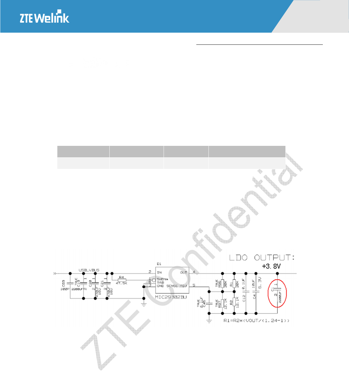
As is shown in the following figure, using LDO power supply circuit as a reference,
over-current capability
of LDO
needs to be above 3A.
As the poor transient response of linear regulator, large capacitors should
be placed at the input and output of LDO to avoid resetting or power off resulted from that too large
voltage fluctuation in high-power transmitting process under GSM mode. The reference power supply
circuit design with LDO is as shown in Figure below.
Figure 4-3 LDO Power Supply
As is shown in the following figure, use DC/DC switch power and large capacitors (lager than 1000uF) to
ensure the normal working of RF PA (power amplifier) and sufficient transient current under GSM Burst
mode.
The advantage of this reference design is that it can provide well transient current under 2G weak signal
environment to satisfy modules requirements, to prevent device shutdown and Ports re-enumeration as a
consequence of the supply voltage drop.
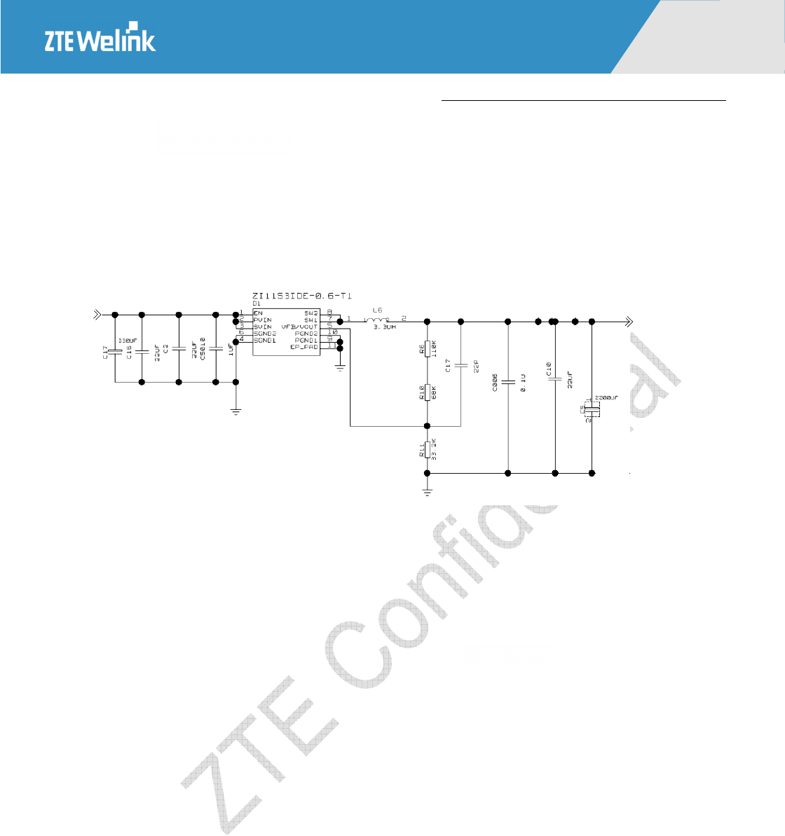
The over-current ability of DC/DC switch power should be larger than 3A such as ZI1153, AAT2138 and so
on. The input voltage range of ZI1153 is 2.5V~5.5V and the output voltage range is 0.6V to VIN (input).
The input voltage range is 2.7V~5.5V and the output voltage range is 3.3V~5.5V.
Hardware Development Guide of Module Products
All Rights reserved, No Spreading abroad without Permission of ZTEWelink 30
MW3650
0
As shown in the Figure below, use DC/DC switching power supply ZI1153 as the buck chip. Place a
tantalum capacitor of 330UF at the input of the chip. Place a 2200UF capacitor or place several 330UF
tantalum capacitors in parallel. This circuit fully meets the module power requirements. (If the user’s PCB
size is limited, the output of buck chip can place three more 330UF tantalum capacitors of which the total
capacity is more than 1000uF)
Figure 4-4 DC/DC Switching Power Supply
Vin=5V Vout=3.8V
4.4.2 VREF PINS
MW3650 module has 2 power output pins used to supply power for external circuit on the mainboard. The voltages of
these pins and the voltages of baseband processor and storage come from the same internal voltage regulator. They
output voltage only when the module is powered on. The normal output voltage is PIN5 (VREF_1V8,1.8V) and
PIN4(VREF_2V8,2.85V). Users should draw current as less as possible from these pins. Generally, users are
suggested that these power pins are only used for pulling up chip pins in level matching process.
4.4.3 PCB Layout Guideline of Power Supply
When design the power supply of module, the layout and wiring of related components in power supply part is very
important. If they are not designed appropriately, it will have effects on many aspects, such as the EMC performance ,
the transmission modulation spectrum, receive sensitivity and so on.
The users of Modules should do as the following guidelines in the process of power supply PCB line designing:
The use of a good common ground plane is suggested.
Because the power switch has strong EMC interference, place the circuit lines far away from antenna.
Hardware Development Guide of Module Products
All Rights reserved, No Spreading abroad without Permission of ZTEWelink 31
MW3650
0
Considering the module power supply requirements, the PCB traces from the input connector to the power regulator
IC must be wide enough to ensure no voltage drops occur when the 2A current peaks are absorbed. The recommended
power wiring width is more than 100mil.
The wiring of power supply should be far away from the circuit which is sensitive for noise such as
microphone/earphone, RF cable and so on.
The PCB wiring between module and bypass capacitor should be wide enough and as short as possible to ensure there
is no significant voltage decline abruptly when the current is peak 2A.
4.5 Power-on/Power-off & Reset
4.5.1 Power On
After the module been normally electrified, it is in power-off status.
To turn on the module, the ON/OFF pin must be tied low for at least 3 seconds and then released.
4.5.2 Power Off
To turn off the module the ON/OFF pin must be tied low for at least 3 seconds and then released.
The power on/off part circuit reference design is shown in the following figure.
Figure 4-5 Power On & Reseting Circuit Reference Diagram
Hardware Development Guide of Module Products
All Rights reserved, No Spreading abroad without Permission of ZTEWelink 32
MW3650
0
4.5.3 Reset
You can reset the module by driving the PON_RESET_N to a low level voltage for more than 100ms and then
releasing. After resetting, the module will shut down first and then enter power-on status automatically.
Other advises
To ensure that the data of module is well saved a, please do not cut off the module power during the module runtime.
It is strongly recommended that use AT command (+ZPWROFF) to shut down the module in application.
The PON_RESET_N and ON/OFF signals are sensitive. When designing a circuit on the PCB of the main board, it is
recommended that the circuit length not exceed 20 mm and the circuit be kept at a distance of 2.54 mm (100 mil) at
least from the PCB edge. Furthermore, you need to surround (on both sides) the signals with Ground. Otherwise, the
module may be reset due to interference.
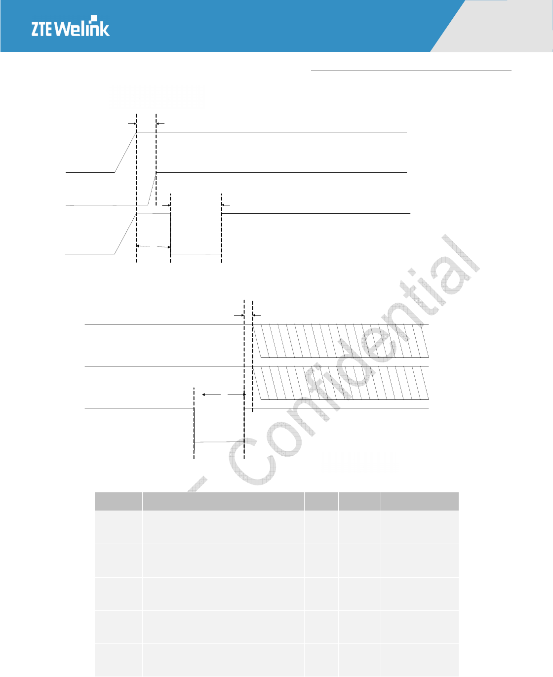
4.5.4 Power-on/Power-off Flow
To guarantee the user can power on and power off stably, you can refer to the power-on sequence chart as shown in
Figure 4-6 and the power-off sequence chart as shown in Figure 4-7. Table 4-3 shows the power-on and power-off
time. During the process of power on the module, pay attention to the following items:
1) The power on time that the module supplies to external interfaces cannot be earlier than the module power on
time.
2) Once the V_MAIN is powered on, the ON/OFF signal will be synchronized and established as the high PWL.
3) The time interval between the V_MAIN is electrified normally and ON/OFF signal is valid could not be too short.
For details see T2 parameter. It is recommended not to disconnect the power supply after V_MAIN is powered
off.
4) The failing edge of ON/OFF is the start of power-on time. ON/OFF should be released after being kept at low
PWL for a period of time.
5) VBUS supplies power for USB PHY. It is not recommended to connect VBUS to power supply before V_MAIN.
During the process of power-off, pay attention to the following items:
1) To power off by the ON/OFF signal, the T4 period needs to be designed as required.
2) After VPH_PWR and USB_VBUS are powered off, it is recommended not to disconnect the power supply.
Hardware Development Guide of Module Products
All Rights reserved, No Spreading abroad without Permission of ZTEWelink 33
MW3650
0
Figure 4-6 Power-on Sequence Chart of Module
V_MAIN
VBUS
ON/OFF
T1
T2
T3
Figure 4-7 Power-off Sequence Chart of Module
ON/OFF
T5
T4
V_MAIN
VBUS
Table 4-3 Power-on/Power-off Time
Parameter Description Min Typical Max Unit
T1 The time from power-on issue to VBUS
ready 0 0.5 1 second
T2 From powering on V_MAIN to ON/OFF
ready 1 1.5 -- second
T3 The time of active low level impulse of
ON/OFF pin to power on module -- 3 -- second
T4 The time of active low level impulse of
ON/OFF pin to power off module -- 3 -- second
T5 The time from power-off issue to
V_MAIN and VBUS off 1 2 -- second
Hardware Development Guide of Module Products
All Rights reserved, No Spreading abroad without Permission of ZTEWelink 34
MW3650
0
4.6 UART Interface
The module provides a series of UART interfaces. The highest speed is 230.4Kbps and the typical speed is 115.2Kbps.
The external interface PWL is 1.8V CMOS PWL signal used for UART communication.
The definition and interface mode of UART are shown as followed.
Table 4-4 The Definition of UART Signal
PIN No. Type Definition I/O Description
53
UART(1.8V)
UART_TXD O UART Send
54 UART_RXD I UART Receive
55 UART_RTS O Send get ready
56 UART_CTS I Receive get ready
57 UART_DSR O Data equipment get ready
58 UART_DTR I Data terminal get ready
59 UART_DCD O Data carrier wave detect
60 UART_RI O Ring indication
NOTE:
1) When the module communicates with PC or MCU trough UART, please pay attention to the direction of TX and
RX. TX and RX is named in the reference direction of module.
2) The sleep of UART is realized through UART_DTR pin. When the module needs sleep, please set this pin as
high PWL while when the module needs to be waked-up, please set this pin as low PWL.
3) When there is SMS, the RI pin will generate low PWL interrupt.
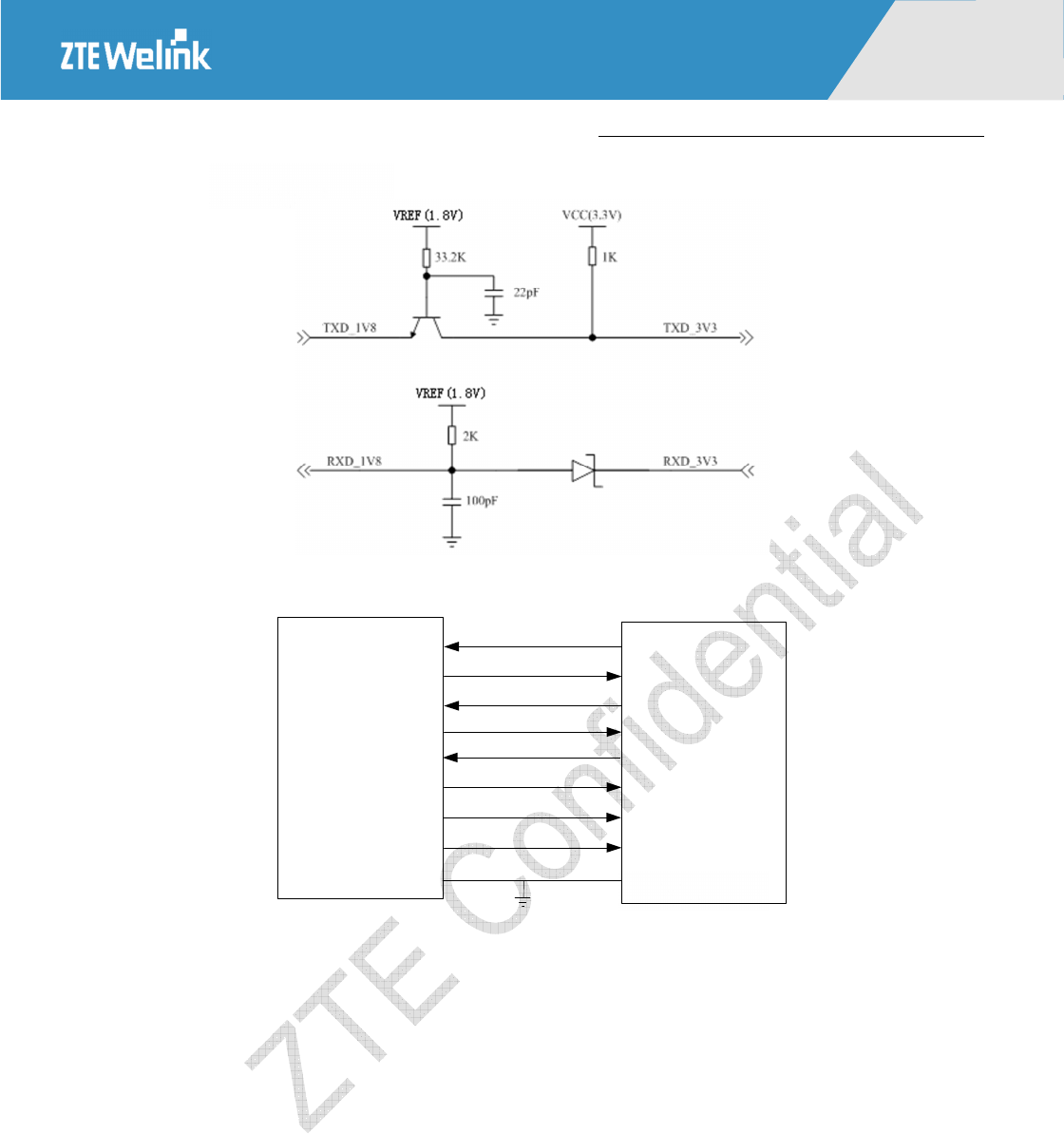
4) MW3650 UART interface supports 1.8V voltage, so the external UART interface which is not 1.8V needs PWL
conversion. As is shown in the following figure, audion can be used to realize the PWL conversion. The
resistance is only an example in the figure. Please recount it during designing. The diode in the figure is Schottky
diode (whose forward voltage drop is 0.3V). If other diodes are chosen, please choose the one whose forward
voltage drop is small to ensure the PWL of RXD_1V8 is below the low PWL input threshold when the low PWL
is input.
Hardware Development Guide of Module Products
All Rights reserved, No Spreading abroad without Permission of ZTEWelink 35
MW3650
0
Figure 4-8 UART Interface PWL Conversion Reference Design
Figure 4-9 Module Serial Port & AP Application Processor
Module AP
RXD
RXDTXD
TXD
CTS
RFR CTS
RFR
DTR
DSRDSR
DTR
DCD
RI RI
DCD
GND GND
To catch LOG during the software debugging process, it is recommended for users to keep this interface and reserve
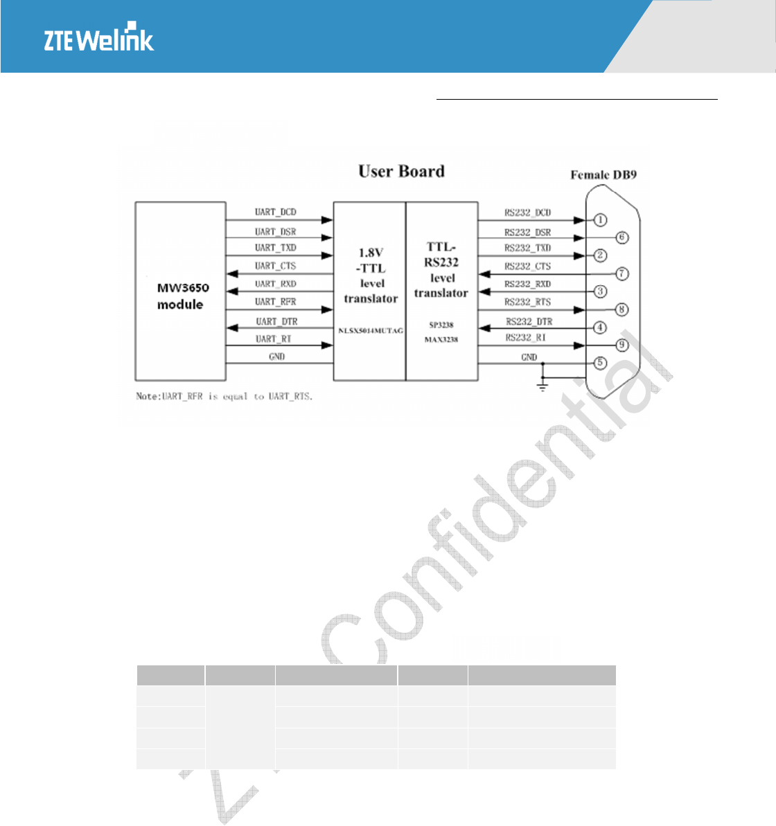
testing points. If the module is connected with the application processor whose PWL is 1.8V, the connection way is as
shown in figure 4-9. 8-line or 2-line connection way can be adopted. The PWL of module interface is 1.8V. If it does
not match with the AP interface, the PWL switching circuit is suggested to be added. MW3650 module can connected
with standard RS-232-C interface through chips of 232 type. If the design is related to the interconverting between
TTL PWL and EIA PWL, the NLSX5014MUTAG chip is recommended to be used. For example, when 2-line UART
is used, the MAX3232 chip is recommended and when 8-line UART is used, SP3238 or MAX3238 chip is
recommended to design the interface. The connection way is shown in the following figure.
Hardware Development Guide of Module Products
All Rights reserved, No Spreading abroad without Permission of ZTEWelink 36
MW3650
0
Figure 4-10 The Connection of UART and Standard RS-232-C Interface
The module support standard 8-wire UART interfaces and transfer digital signals, please isolate them from sensitive
signals to avoid influencing other analog signal and RF signal.
4.7 (U)SIM Card Interface
Module baseband processor integrates the (U)SIM card interface to compliance with ISO 7816-3 standards, and
supports 3.0V/1.8V (U)SIM cards. The signals on SIM card interface is as shown in Table below.
Table 4-5 The Definition of USIM Card Interface
PIN No. Type Definition I/O Description
37
USIM
USIM_CLK O USIM card clock line
38 USIM_DATA I/O USIM card data line
39 USIM_RST O USIM card reset signal
40 VREG_USIM O USIM 1.8/3V power supply
Notes about designing SIM card:
1) Because the typical speed of (U)SIM card interface is about 3.25MHz, it is recommended to place (U)SIM card
console close to the (U)SIM card interface, to prevent the wiring from being too long (the wiring is recommended
not to be longer than 100mm) to influence the normal communication of (U)SIM signal.
2) The wiring of SIM card signal wire should be placed far away from RF wire and V_MAIN power supply line.
3) The GND of SIM card console wiring and the module GND wiring should be short and thick, meanwhile the
electric potential of them should be the same. The line width of SIM_VDD and GND should be ensured not less
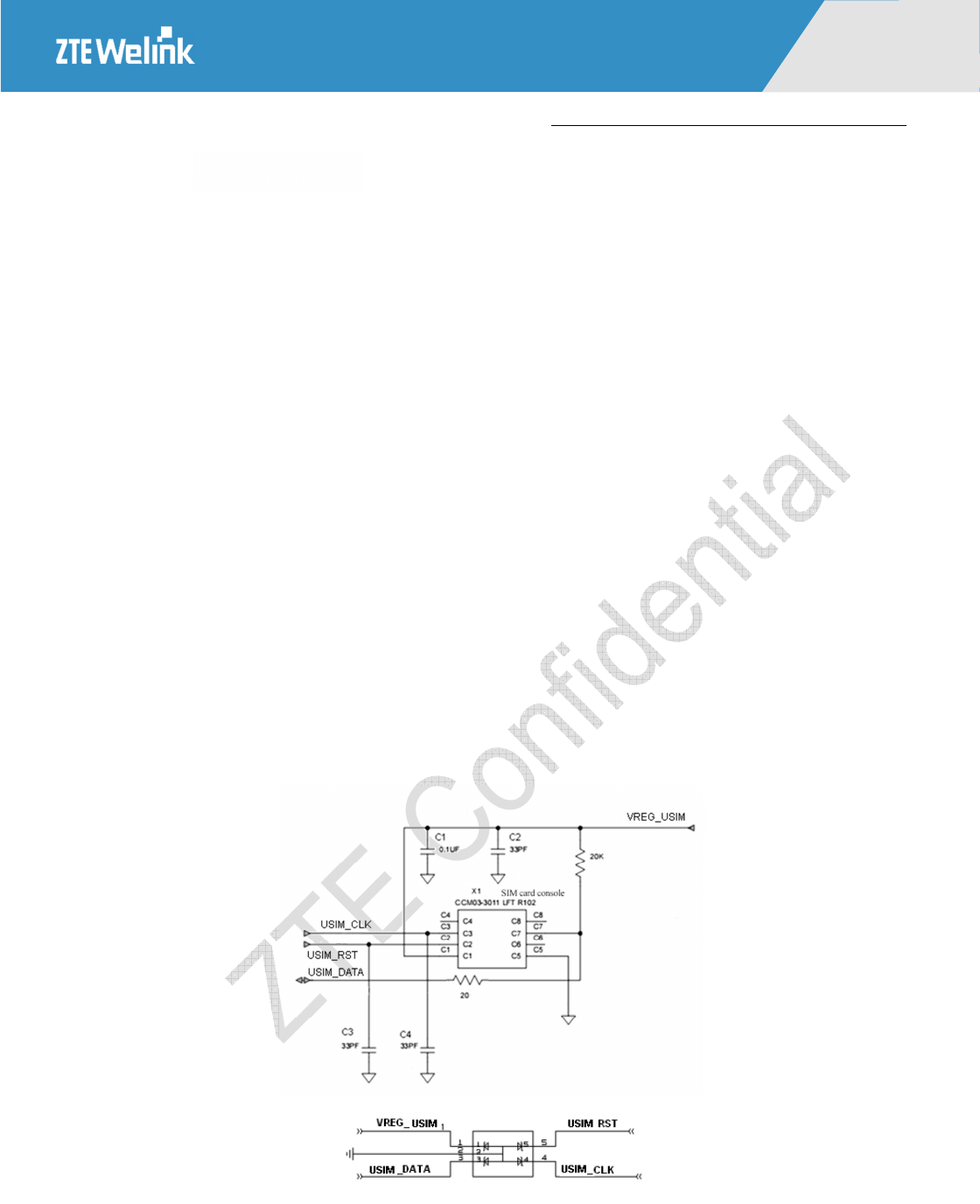
Hardware Development Guide of Module Products
All Rights reserved, No Spreading abroad without Permission of ZTEWelink 37
MW3650
0
than 0.5mm. The bypass circuit between VREG_USIM and SIM_GND should not be bigger than 1uF, and be
placed near the SIM card console.
4) To avoid the potential interference between USIM_CLK and USIM_DATA signal, please do not place the wiring
of them too near, and USIM_CLK and USIM_DATA signal need to be surrounded by Ground. USIM_RST
signal also needs ground protection. Add a 0.1uF or 0.22uF capacitance of 0402 encapsulation on VREG_USIM,
and cascade a 0Ω resistance and parallel a 33pF capacitance with USIM_CLK, USIM_DATA and USIM_RST
for the convenience of matching of latter electrical performance and to avoid the interference because of too long
wiring. Besides, USIM_DATA signal should be pulled up to VREG_USIM. The pull-up resistor value is about
10K to avoid the identification problem of SIM card.
5) Besides, these four signal wires should parallel TVS to avoid electrostatic discharge. The recommended reference
design circuit of ESD protection of wireless module SIM card interface is shown in the following figure.
6) The wiring related to (U)SIM card need to be put together. The wiring width of VREG_USIM is related to its
length. The recommended value is 10 mil wiring width. The wiring of (U)SIM card can refer the wiring of BUS.
Please pay attention to the wiring protection to avoid the interference of high-speed signal and strong reference
signal of clock to (U)SIM card signal. Otherwise the restart of (U)SIM card may be caused. The ESD protection
components of (U)SIM card should be placed near (U)SIM card console to avoid the electrostatic interference to
module.
Figure 4-11 (U)SIM Card Console Circuit Reference Design

Hardware Development Guide of Module Products
All Rights reserved, No Spreading abroad without Permission of ZTEWelink 38
MW3650
0
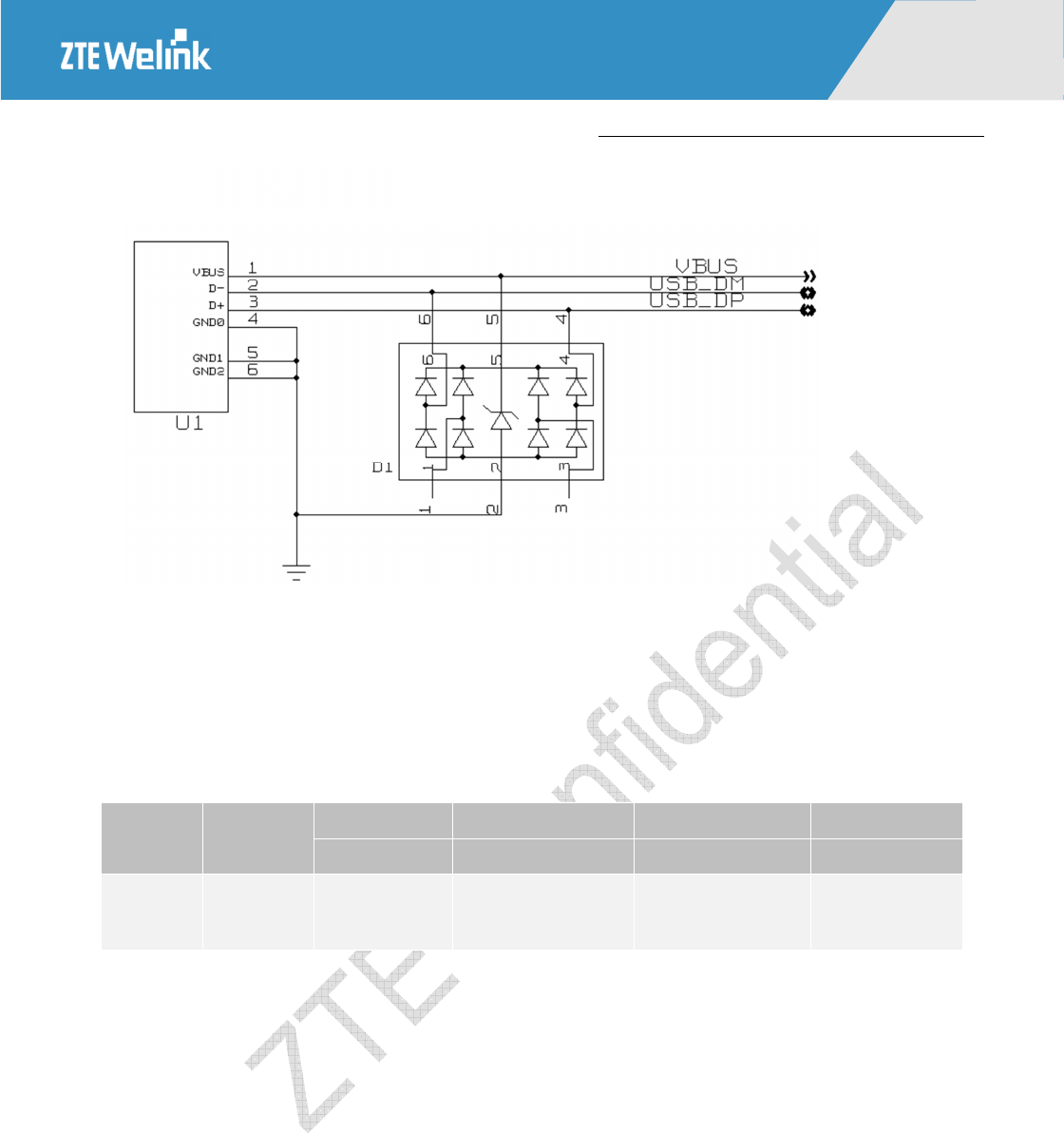
4.8 USB Interface
MW3650 module has the high-speed USB2.0 interface. It is connected to the system board side by LCC interface,
which is the path for communication between the processor on the system board side and module of which the pins
are PIN23(USB_DM) and PIN24(USB_DP). The definition of USB pins is shown in table 4-6.
Table 4-6 The Definition of USB PINS
PIN NO. Type Definition I/O Description Remark
22
USB
VBUS I USB power 5V
23 USB_DM I/O USB data- --
24 USB_DP I/O USB data+ --
VBUS is the module USB power supply pin. The working current of USB is 4.75V~5.25V and typical value is
5V.This power supply can supply the module with 3.8V voltage after transition by the power supply circuit mentioned
in the previous section. USB_DM/USB_DP is differential data line. During PCB wiring, it should meets the
requirements of differential line and surrounded by Ground. If it is too close to antenna, to avoid the influence of
antenna radiation, high-speed common mode suppression filter can be concatenated on the USB differential signal
wiring circuit.
USB interface needs to add TVS components to avoid damage of module components because of static electricity.
The load capacitance value of TVS should be less than 3pF, to satisfy the transmission of USB2.0 high-speed signal.
In the following figure, D1 is USB2.0 anti-static protective components.
Meanwhile, USB_VBUS pin is vulnerable to voltage shock which can damage the pin. It is recommended to adopt
appropriate OVP measure to avid the voltage higher than 5.25V. Besides, the power-off leakage current exists on
USB_VBUS. It is suggested to add power switch on power supply branch circuit or cascade a resistance with the
resistance value between 200kΩ and 400kΩ to reduce the leakage current when the module is powered off but does
not cut off the power.
Hardware Development Guide of Module Products
All Rights reserved, No Spreading abroad without Permission of ZTEWelink 39
MW3650
0
Figure 4-12 USB Interface Circuit Reference Design Schematic Diagram
Usually, USB interface of module can be enumerated to several ports, such as AT port, DIAG port, Modem port and
so on. These ports are enumerated in order during the load process. For example, during the load process of module
under Linux system, if the enumeration of DIAG port is ttyUSB0, the ports maps on PC are shown in the following
table.
Table 4-7 The Correspondence of Port Map
Module VID&PID Dial-up port AT Command Port DIAG Port Audio Port
USB Modem Service Port Diagnostics Port Voice Port
MW3650 VID_19D2&
PID_FFEB
Windows: 03
/Linux: ttyUSB3
Windows: 02
/Linux: ttyUSB2
Windows: 00
/Linux: ttyUSB0
Windows: 01
/Linux: ttyUSB1
USB Modem port, bearing AT commands, is mainly used for initiating data business.
Service Port, bearing AT commands, is mainly used for AT command operation when MODEM port is occupied by
data business.
Diagnostics Port, bearing DIAG task, can be connected to the tool for catching LOG or updating to catch software
LOG information or update the firmware.
4.9 Working Status Indicator Interface
The SIG_LED pin is constant current output interface whose current driver capability is 20mA. It is connected with
LED to indicate the working status of module.
Hardware Development Guide of Module Products
All Rights reserved, No Spreading abroad without Permission of ZTEWelink 40
MW3650
0
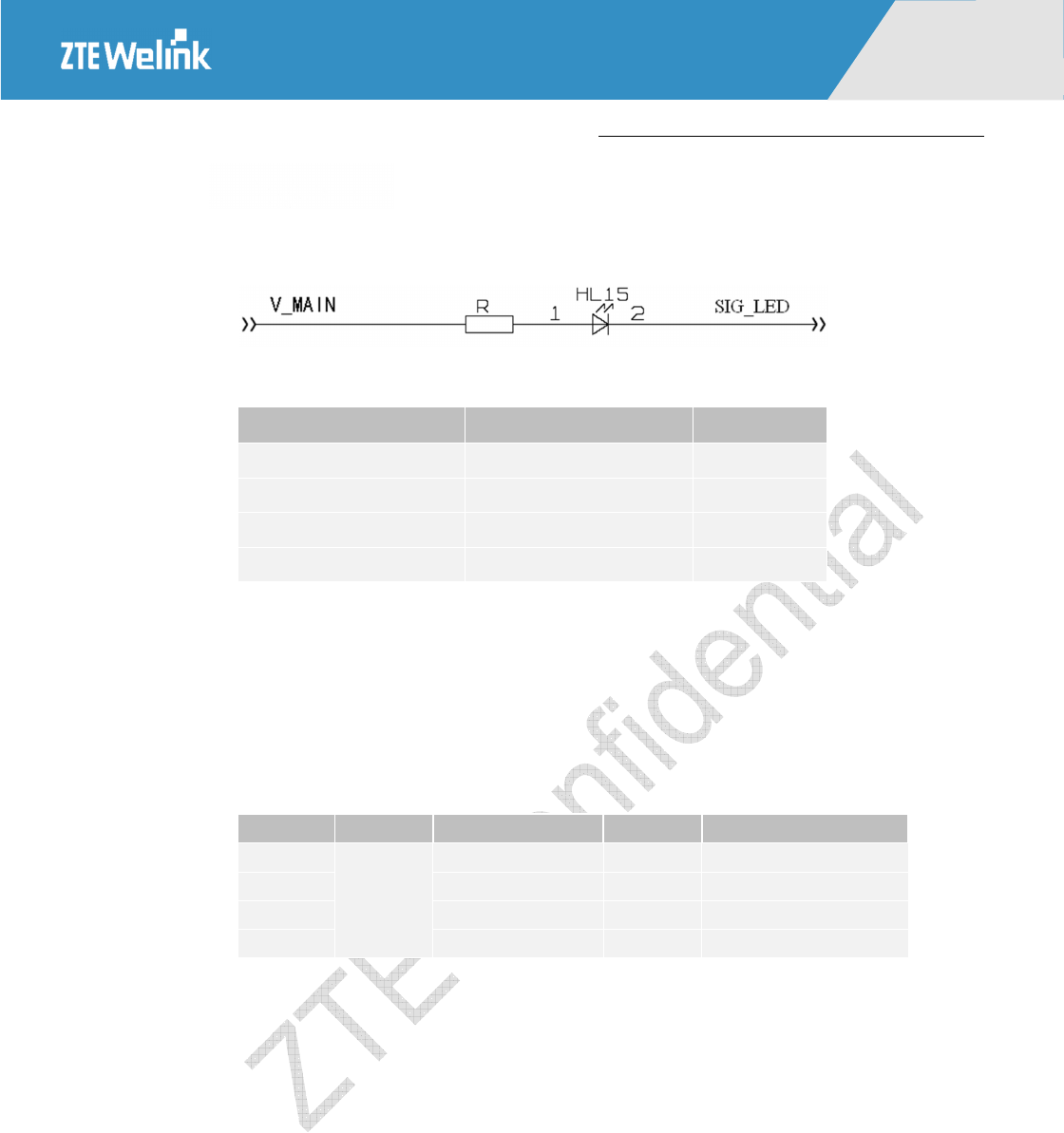
The indicator light reference design is shown in the following figure. The luminance of LED can be regulated by the
value of resistance. The indicator status of network is as defined in table below
Table 4-8 Indicator Light Reference Design Schematic Diagram
Table 4-9 The Description of Working Status Indicator Light
Module status Indicator light status Frequency
Power-on status Indicator light off
Network searching status Standard flicker 3Hz
Free status Slow flicker 1Hz
Data business status Fast flicker 5Hz
4.10 SPI Bus Interface
The SPI interface signal definition of this product is shown in the following table.
Table 4-10 The Definition of SPI Interface
PIN NO. Type Definition I/O Description
32
SPI
SPI_MISO_DATA -- Main input, slave output
33 SPI_MOSI_DATA -- Main output, slave input
34 SPI_CLK I/O SPI interface clock signal
35 SPI_CS_N I/O SPI gating signal
SPI interface electric features:
The SPI bus of this product is configured as the main equipment, which has three modes:
Running mode—basic running mode;
Waiting mode— The waiting mode of SPI is a configurable low-power mode, enabled by the byte of the control
registered. In the waiting mode, if the waiting byte is cleared, SPI works under the similar running mode. However, if
SPI waits for the position byte, SPI clock stops and enters the low-power status.
Hardware Development Guide of Module Products
All Rights reserved, No Spreading abroad without Permission of ZTEWelink 41
MW3650
0
Stop mode—Under the stop mode, SPI is not available, so the power consumption is reduced. If SPI is configured as
the master equipment, any transmission process will be stopped, but it can enter the running mode when the waiting
mode stops.
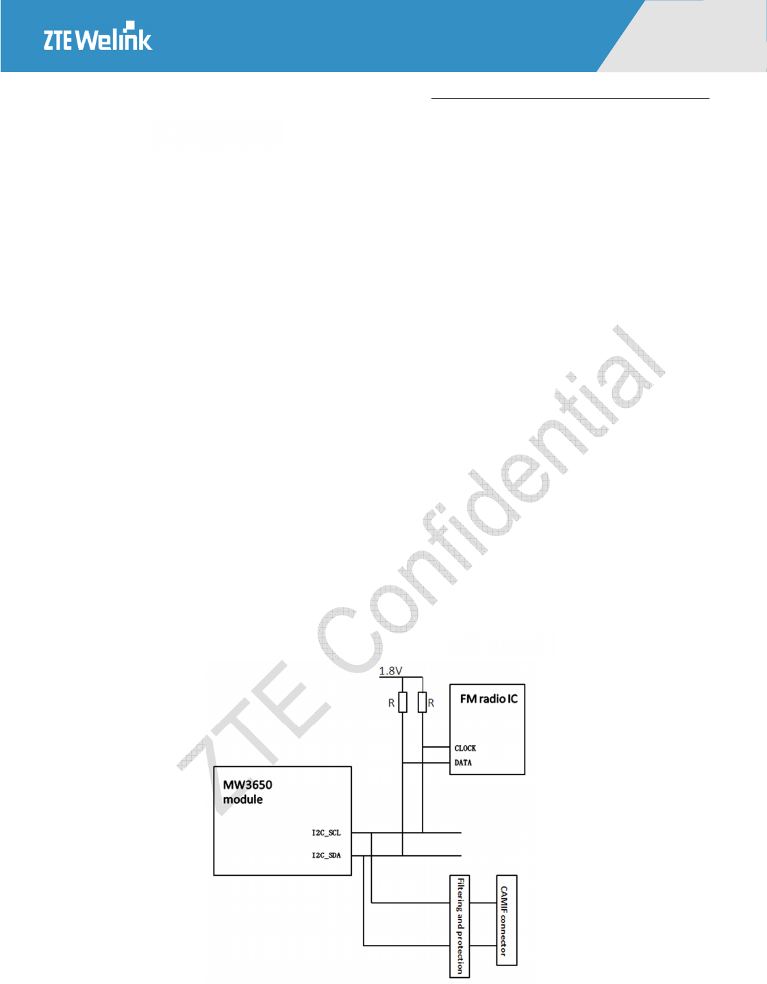
4.11 I2C Bus
I2C is the two-wire bus for the communication between ICs, which supports any IC process (NMOS, CMOS,
dual-polarity). The two signal wires, serial data (I2C_SDA) and serial clock (I2C_SCL), can transmit information
between the connected equipment. Each equipment is identified by the unique address (such as the micro controller,
storage, LCD driver or keyboard interface). Due to the different functions of the equipment, it can be used as both the
sender and the receiver.
The I2C interface has the following electric features:
1) The two-wire bus is used for the communication between chips.
2) It supports any external equipment of any manufacturing technology (1.8V).
3) It supports the external functions, such as the image sensor, micro controller, LCD driver and
keyboard interface.
The I2C interface has two working modes with different transmission ratios: standard mode with a speed as high as
100kbps; high-speed mode with a speed as high as 400kbps. Figure 4-11 is the I2C reference circuit design diagram.
Table 4-11 I2C Reference Circuit Design

Hardware Development Guide of Module Products
All Rights reserved, No Spreading abroad without Permission of ZTEWelink 42
MW3650
0
4.12 User Interface
AT commands are mainly used for communication between users and the module. AT commands comply with ITU-T
V.250, 3GPP 27.007 and 3GPP 27.005 standards. Moreover, the module also supports ZETWelink expanding AT
commands.

Hardware Development Guide of Module Products
All Rights reserved, No Spreading abroad without Permission of ZTEWelink 43
MW3650
0
5
Antenna
5.1 Preliminary Antenna Evaluation
The antenna is a sensitive device and its performance is greatly affected by external environments. The radiation
performance of the antenna is affected by the mainboard dimensions, antenna position, occupied space size of the
antenna, and the grounding of surrounding components of the antenna. Besides, the fixed assembly of the antenna, the
wiring of RF cables on the antenna, and the fixed position of the antenna all are related to the problem whether the
antenna exists the interference problem with structure. Thus, during the preliminary design phase of an antenna, it is
critical that antenna engineers, RF engineers, baseband engineers, structure engineers, and ID engineers work together
to make estimation for both 2D and 3D design.
5.2 Antenna Design Guidance
Well shielding measure should be added between external antenna and RF PAD of module, and external cables should
be far away from all interference source, especially high-speed digital signal, DC/DC power and so on.
According to mobile equipment standard, the standing-wave ratio of antenna the module uses should be between 1.1
and 1.5. Input resistance is 50Ω. Under different environments, the requirements of antenna gain are different. Usually,
antenna performance is better if intraband gain is larger and out-of-band gain is smaller. When using the multi-ports
antenna, the isolation between the ports should be larger than 30dB. For example, the isolations between the two
different polarization ports on polarization antenna, the two different frequency ports on dual-frequency antenna and
the four ports on dual-frequency dual-polarization antenna should be larger than 30dB.
Hardware Development Guide of Module Products
All Rights reserved, No Spreading abroad without Permission of ZTEWelink 44
MW3650
0
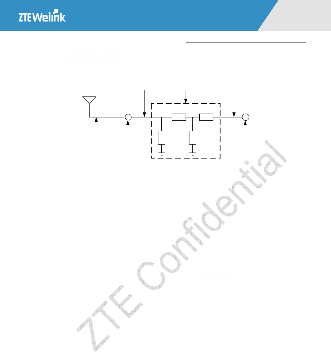
Figure 5-1 Translation Circuit Diagram
Microstrip line or
stripline with a
natural impedance of
50 ohm
Microstrip line or
stripline with a
natural impedance of
50 ohm
Dual-L matching
network
RF coaxial cable of
the antenna
RF interface on the
antenna RF cable
and RF interface on
the mainboard
RF interface on
the module
Anten
na
PIN62 is antenna pin. The following items should be noticed when this pin is used an antenna feed pin.
1) The feed cable connected with PIN 62 is microstrip line or strip line with resistance value of 50Ω. Near the
module, π-shaped or inverted-F-shaped matching network should be added for latter tuning.
2) The RF wiring should be kept certain distance with GND. Usually the distance is 3 times the line width of RF
wiring.
3) Do not pile the interference sources near the RF wiring or RF ports, such as DCDC, WIFI module and so on.
5.3 Suggested Antenna Location
Mainboard area has serious interference. The experiments result shows that the module performance will be poor If
the module is placed in these interference regions. During the laptop design, it is better to separate the module from
the mainboard PCB, instead of installing the module on the mainboard. If they cannot be separated, the module should
be far from modules and components that might generate EMI, such as chip and memory, power interface, and data
cable interface.
For Internet laptops products, the ideal position of antennas is on the top left corner or top right corner of the LCD,
which is relatively far from the mainboard, so the electromagnetic interference is relatively small. Besides, because it
is far from human bodies, it is easy to satisfy SAR indexes. The other choice is on the left or right of LCD. Other
products such as router, e-book and so on should be evaluated specifically according to the features of product itself.

Hardware Development Guide of Module Products
All Rights reserved, No Spreading abroad without Permission of ZTEWelink 45
MW3650
0
Because different antenna manufacturers may adopt different antenna modes and different terminal products have
different external dimension and different requirements for antenna performance, the reserved spaces as well as
antenna dimension and location are all different. Take the 3G internet laptops as an example, the recommended
antenna space dimension is larger than 7mm*10mm*100mm, and it is recommended to place the antenna at the top of
LCD screen.
5.4 RF PCB wire guidelines
The RF wiring of antenna should be kept as short as possible. It is suggested to choose thicker RF cables considering
the transmission consumption. Meanwhile, RF cables should be far away from modules and components that might
generate EMI, such as chip and memory, power interface, and data cable interface. The RF wiring connecting the
antenna and 3G module should not be right angle, squeezing and abraded.
Keep, if possible, at least one layer of the PCB used only for the Ground plane; If possible, use this layer as reference
Ground plane for the transmission line;
5.5 EMC Requirements
Electronic communications have more EMC requirements than non-communication products. It is very important that
baseband engineer, RF engineer and antenna engineer must fully communicate during the design process of circuit
and wiring to reduce the electromagnetic interference of produces. The following items are common problems and
solutions that can be referred during the product design process.
1) During the product design, it is better to separate the module from the mainboard PCB, instead of installing the
module on the ground of the mainboard. If they cannot be separated, the module should be far from modules and
components that might generate EMI, such as chip and memory, power interface, and data cable interface.
2) Because the mainboard of PAD, CPE, and Internet laptops does not have a shielding cover, as that of mobile
terminals, to shield most circuits to avoid overflow of electromagnetic interference, you can spray conductive
paint on the surface on non-antenna areas within the structural components above and below the mainboard, and
the conductive paint should be connected to the ground on the mainboard by several points to shield
electromagnetic interference.
3) Besides, data cables of the LCD and the camera might introduce interference signals, which affect the receiving
performance of the antenna. Thus, it is necessary to wrap conductive cloth around the two data cables and
connected them to the ground.

Hardware Development Guide of Module Products
All Rights reserved, No Spreading abroad without Permission of ZTEWelink 46
MW3650
0
4) RF cables of the antenna should be far from modules and components that might generate EMI, such as chip and
memory, power interface, and data cable interface. The wiring of RF cables should be close to the ground of the
mainboard.
5.6 Index Requirement of Antenna
Module supported electronic communications pay more and more attention to collect radiation performance test. At
present there are two methods to investigate the radiation performance: one method is investigating the radiation
performance of antenna which is a traditional antenna test method, i.e. passive test; the other method is testing the
radiation power and receiving sensitivity in a specific microwave darkroom, i.e. active test.
The index requirement of antenna involves passive index requirement and active index requirement. Passive indexes
include S11, antenna efficiency, antenna gain, antenna pattern and so on which can used as parameters weighing the
performance of antenna itself. Active indexes usually mean OTA indexes, including TPR (all-round radiation power),
TIS (all-round receiving sensitivity), radiation pattern and so on which are important indexes weighing the whole
device (including antenna, module, circuit main board) radiation performance.
5.6.1 Passive Index of Antenna
Different products have different requirements about antenna performance. The following is the passive reference
index about PAD products while the antenna radiation performance is weighed by the active index. The passive index
requirements are only for the main antenna as is shown in table below.
Table 5-1 The Passive Index Reference of Main Antenna about PAD product
Frequency band 824-960MHz 1710-2170MHz
VSWR <3.5:1 <3.5:1
Maximum gain >0dBi >0dBi
Average gain >-3.5dBi >-3.5dBi
Efficiency >40% >40%
It is recommended that the passive index reference of diversity antenna should be decided by the requirements of its
performance. If it is required that the performance of diversity antenna is the same as the performance of main antenna,
the requirement about passive index of diversity antenna is shown in table above. If it is required that the performance
of diversity antenna reach half of performance of main antenna, see table below for passive index.
Table 5-2 The Passive Index Reference of Diversity Antenna about PAD product
Frequency band 824-960MHz 1710-2170MHz

Hardware Development Guide of Module Products
All Rights reserved, No Spreading abroad without Permission of ZTEWelink 47
MW3650
0
VSWR <3.5:1 <3.5:1
Maximum gain >-3dBi >-3dBi
Average gain >-6.5dBi >-6.5dBi
Efficiency >20% >20%
NOTE:
MW3650 module does not support diversity reception.
5.6.2 Active Index of Antenna
Active index is an important index weighing the radiation performance of whole device (including antenna, module
and circuit main board), so the active index decides the final radiation performance of product. Because different
products have different active index and different operators have different requirements about active index, it is
suggested that antenna engineer, RF engineer, baseband engineer, structure engineer and ID engineer evaluate the
performance the whole device can achieve according to the requirements customer provides about the product
performance in the beginning of a project to decide the active index. For mobile terminal product, there is no
international general standard. The standards are all customized according to the requirements of operator. Table 5-4
is the active index provided by our company for mobile terminal products for reference.
Table 5-3 Recommended Product OTA Index Requirement
Mode Frequency band TRP(dBm) TIS(dBm)
Free space Free space
GSM
GSM850MHz 28 -104
GSM900MHz 28 -104
GSM1800MHz 26 -102
GSM1900MHz 26 -102
WCDMA
Band I 19 -106
Band II 19 -104.5
Band V 19 -104.5
Band VIII 19 -104.5
The active index reference of diversity antenna should be decided by the performance of diversity antenna.
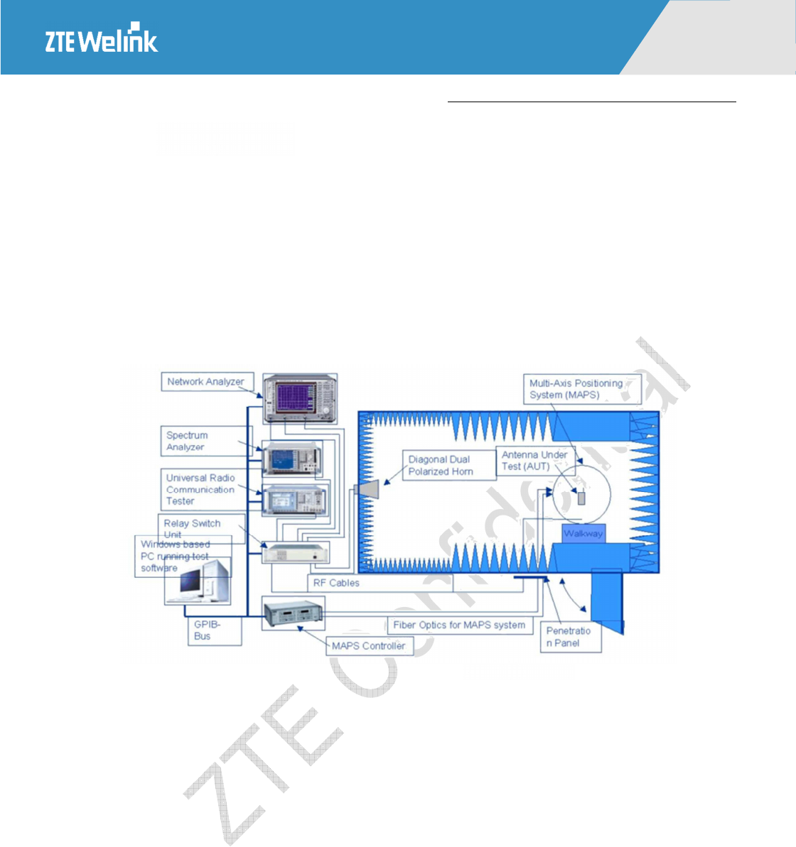
Hardware Development Guide of Module Products
All Rights reserved, No Spreading abroad without Permission of ZTEWelink 48
MW3650
0
5.6.3 OTA Test method of Whole Machine Antenna
Refer to the OTA test method of corresponding products in CTIA. Figure 5-6 is the structure of OTA test system in
CTIA. This system mainly consists of darkroom, high-precision location system and its controller, RF test instrument
and PC with automatic test program. The main RF instruments involve integrated testing instrument, frequency
spectrograph and network analyzer.
The frequency spectrograph, swivel table controller and PC with automatic test program communicate with each other
through GPIB interface.
Figure 5-2 OTA Test System
Hardware Development Guide of Module Products
All Rights reserved, No Spreading abroad without Permission of ZTEWelink 49
MW3650
0
6
Electric Feature
This section mainly introduces the electric features of the module, including module interface PWL, power dissipation,
reliability and so on.
6.1 Interface PWL
See table 6-1 for the main outward interface PWL of the module.
Table 6-1 Main Out ward Interface PWL of Module
Interface PWL Min Typical Max
UART 0 -- 0 0.1*V_UART
1 0.9*V_UART V_UART --
UIM 0 -- 0 0.1*VREG_USIM
1 0.9*VREG_USIM VREG_USIM --
V_UART is 1.8V, VREG_USIM is 1.8V or 3V. Please design according to the CMOS interface PWL.
6.2 Power Supply
The input voltage range of MODULE is DC 3.4V~4.2V, and the typical value is 3.8V as shown in Table6-2.
Table 6-2 Input Voltage
Parameter Min Typical Max
Input voltage 3.3V 3.8V 4.2V
6.3 Working Current
The working current range of module is as shown in Table 6-3. The Sleep mode indicates the power consumption of
the module in standby and sleep mode. The table also provides the working current range under GSM and WCDMA
mode when there is data service.

Hardware Development Guide of Module Products
All Rights reserved, No Spreading abroad without Permission of ZTEWelink 50
MW3650
0
Table 6-3 The Current Consumption under Sleep Mode
Mode Frequency Band Test value (mA) Remark
WCDMA
Band I (IMT2100) <5
Sleep mode
Band II (PCS1900) <5
BandV(850) <5
BandVIII(900) <5
GSM
GSM1900 <5
GSM1800 <5
GSM900 <5
GSM850 <5
Note:USB bus is fully suspended under this mode. In this mode, the module can also accept
SM from the network. The power consumption is decreased to the lowest level. The above test
value is the average current acquired under the maximum transmission power. Under different
environments, the testing results might be slightly different. Take the actual situation as the
reference.
Table 6-4 The Working Current of MODULE
Mode Frequency Band Test value (mA) Remark
UMTS
Band I (IMT2100) 540
The module in
state of working.
Band II (PCS1900) 530
BandV(850) 389
BandVIII(900) 537
GSM/GPRS
GSM1900 226
The module in
state of working.
GSM1800 169
GSM900 239
GSM850 239
Note: The above test value is the average current acquired under the maximum
transmission power. Under different environments, the testing results might be slightly
different. Take the actual situation as the reference.
Hardware Development Guide of Module Products
All Rights reserved, No Spreading abroad without Permission of ZTEWelink 51
MW3650
0
7
Technical Index of Radio Frequency
Test Environment:
Test instrument: Agilent 8960
Power supply: Agilent 66319D
RF cable length: About 15 cm
WCDMA 850 MHz/900 MHz compensation: 0.6dB
WCDMA 2100 MHz/1900 MHz compensation: 0.8dB
NOTE:
The compensation value is set by the frequency characteristic of corresponding RF cable. The compensation mode is
related to the equipment.
7.1 Index of RF under UMTS Mode
The RF index should be tested strictly in accordance with the related testing specifications of 3GPP. The RF indexes
of UMTS2100/1900/850/900 should satisfy the requirements of 3GPP TS 34.121 protocol.
7.1.1 Maximum Transmission Power
Maximum transmission power is another very important index to weigh the module performance. It is the maximum
transmission power the module can transmit tested at the antenna port. Under the normal testing environment, the test
value and reference value of the maximum transmission power of UMTS2100/1900/850/900 are shown in the table
7-1.
Table 7-1 Maximum Transmission Power
Operating Band Level 3GPP Protocol Claim Test value
UMTS850 Class 3 +24dBm +1/-3dBm 23.04
UMTS900 Class 3 +24dBm +1/-3dBm 23.04
UMTS1900 Class 3 +24dBm +1/-3dBm 22.89
Hardware Development Guide of Module Products
All Rights reserved, No Spreading abroad without Permission of ZTEWelink 52
MW3650
0
UMTS2100 Class 3 +24dBm +1/-3dBm 22.45
7.1.2 Receiving Sensibility
The receiving sensitivity is a key parameter that indicates the weakest signal strength the module can receive and
work well with it. At the same time the BER (Bit Error Rate) must meet the 3GPP TS 34.121protocol requirements in
case of the minimum signal. The test value of UMTS2100/900 receiving sensibility is shown in the Table 7-2.
Table 7-2 Reference of Receiving Sensitivity
Operating Band Unit 3GPP Protocol Claim Test value
UMTS850 dBm/3.84 MHz ≤-103.7dBm -109.9
UMTS900 dBm/3.84 MHz ≤-103.7dBm -109.2
UMTS1900 dBm/3.84 MHz ≤-104.7dBm -110.3
UMTS2100 dBm/3.84 MHz ≤-106.7dBm -109.9
7.1.3 Spurious Emission Index
The spurious emission is the signals the transmitter transmits beyond the frequency band the spectrum emission mask
describes. The spurious emission will interfere other wireless communication systems. The aims of meeting the
spurious emission requirements are improving the electromagnetic compatibility performance of the system for better
coexisting of other systems and ensuring the normal running of the system itself. The spurious emission index of
UMTS2100/1900/850(900) should comply with the requirements in 3GPP TS 34.121 protocol, as illustrated below.
And the test result of module in UMTS mode meets the requirement in Table 7-3.
Table 7-3 Spurious Emission Index
Frequency Band Resolution Bandwidth Minimum Requirement
9 kHz ≤ f < 150 kHz 1 kHz -36 dBm
150 kHz ≤ f < 30 MHz 10 kHz -36 dBm
30 MHz ≤ f < 1000 MHz 100 kHz -36 dBm
1 GHz ≤ f < 12.75 GHz 1 MHz -30 dBm
7.2 Index of RF under GPRS/GSM/EDGE Mode
The RF indexes of GSM/GPRS/EDGE 900/1800 should satisfy the requirements of 3GPP TS 05.05 protocol.
Hardware Development Guide of Module Products
All Rights reserved, No Spreading abroad without Permission of ZTEWelink 53
MW3650
0
7.2.1 Maximum Transmission Power
Maximum transmission power is another very important index to weigh the module performance. It is the maximum
transmission power the module can transmit tested at the antenna port. Under the normal testing environment, the test
value and reference value of the maximum transmission power of GSM850/900/1800/1900 (GMSK/8PSK) are shown
in the table 7-4.
Table 7-4 Maximum Transmission Power of GSM850/900/1800/1900 (GMSK/8PSK)
Frequency Band Power Level 3GPP Protocol Claim Test value
GSM850 Class 4 +33dBm±2dBm 32.61 dBm
GSM900 Class 4 +33dBm±2dBm 32.9 dBm
GSM1800 Class 1 +30dBm ±2dBm 30.08dBm
GSM1900 Class 1 +30dBm ±2dBm 29.55 dBm
7.2.2 Receiving Sensibility
The receiving sensitivity is a key parameter that indicates the weakest signal strength the module can receive and
work well with it. At the same time the BER (Bit Error Rate) must meet the 3GPP TS 34.121protocol requirements in
case of the minimum signal. The test value of GSM850/900/1800/1900 (GMSK/8PSK) receiving sensibility is shown
in the Table 7-5.
Table 7-5 Receiving Sensitivity
Frequency Band Unit 3GPP Protocol Claim Test value
GSM850 dBm/3.84 MHz ≤-102dBm -110.3dBm
GSM900 dBm/3.84 MHz ≤-102dBm -110.2 dBm
GSM1800 dBm/3.84 MHz ≤-102dBm -108.3dBm
GSM1900 dBm/3.84 MHz ≤-102dBm -107.3 dBm
7.2.3 Spurious Emission Index
The spurious emission is the signals the transmitter transmits beyond the frequency band the spectrum emission mask
describes. The spurious emission will interfere other wireless communication systems. The aims of meeting the
spurious emission requirements are improving the electromagnetic compatibility performance of the system for better
coexisting of other systems and ensuring the normal running of the system itself. The spurious emission index of
GSM850/900/1800/1900 (GMSK/8PSK) should comply with the requirements in 3GPP TS 34.121 protocol. And the
test result of module meets the requirement in following.
The test power should be less than -36dBM tested under the frequency band between 9kHz and 1GHz.

Hardware Development Guide of Module Products
All Rights reserved, No Spreading abroad without Permission of ZTEWelink 54
MW3650
0
The test power should be less than -30dBm tested under the frequency between 1GHz and 12.75GHz.

Hardware Development Guide of Module Products
All Rights reserved, No Spreading abroad without Permission of ZTEWelink 55
MW3650
0
8
Related Test & Test Standard
8.1 Testing Reference
The related tests of MODULE comply with the IEC standard, including the equipment running under high/low
temperature, storage under high/low temperature, temperature shock and EMC. Table 8-1 is the list of testing standard,
which includes the related testing standards for MODULE.
Table 8-1 Testing Standard
Test Standard Document Reference
IEC6006826 Environmental testing-Part2.6:Test FC: Sinusoidal Vibration
IEC60068234 Basic environment testing procedures part2.
IEC60068264 Environmental testing-part2-64: Test FH: vibration, broadband random
and guidance.
IEC60068214 Environmental testing-part 2-14: Test N:change of temperature.
IEC60068229 Basic environmental testing procedures-part2: Test EB and guidance.
IEC6006822 Environmental testing-part2-2:Test B:dry heat
IEC6006821 Environment testing-part2-1: Test A: cold.
GB/T 15844.2 MS telecommunication RF wireless phone-set environment requirement &
experimental method – part 4: Strict level of experimental condition
GB/T 2423.11
Basic environment experiment of electronic products-Part2:Experiment
method Try Fd: Broad frequency band random vibration (General
requirement)
TIA/EIA 603 3.3.5 TIA Standard-part3-5:Shock Stability
NOTE:
1. IECL International Electro technical Commission;
2. GB/T: Recommended national standard
.

Hardware Development Guide of Module Products
All Rights reserved, No Spreading abroad without Permission of ZTEWelink 56
MW3650
0
8.2 Description of Testing Environment
The working temperature range of MODULE is divided into the normal working temperature range and the extreme
working temperature range. Under the normal working temperature range, the testing result of RF complies with the
requirements of 3GPP specifications, and its function is normal. Under the extreme temperature range, the RF index
basically complies with the 3GPP specifications, and the quality of data communication is affected to a certain extent,
but its normal function is not affected. MODULE has passed the EMC test. Table 8-2 is the requirement for the
testing environment, and Table 8-3 lists out the instruments and devices that might be used during the test.
Table 8-2 Testing Environment
Working Condition Min Temperature Max Temperature Remark
Normal working condition -30°C +75°C All the indexes are good.
Extreme working
condition
-40°C +85°C Some indexes become poorer.
Storage -40°C +85°C Storage environment of module
Table 8-3 Testing Instrument & Device
Testing Item Instrument & Device
RF test Comprehensive testing device
RF cable
Tower antenna
Panel antenna
High/Low-temperature
running & storage test
High/Low-temperature experimental box
Temperature shock test Temperature shock experimental box
Vibration test Vibration console
8.3 Reliability Testing Environment
The reliability test includes the vibration test, high/low-temperature running, high/low-temperature storage and
temperature shock experiment test. Refer to Table 8-4 for the specific parameters.
Table 8-4 Reliability Features
Test Item Test Condition Test Standard
Random vibration Frequency range: 5-20Hz, PSD:1.0m2/s3
Frequency range: 20-200Hz, -3dB/oct
3 axis, 1 hour for each axis
IEC 68-2-6

Hardware Development Guide of Module Products
All Rights reserved, No Spreading abroad without Permission of ZTEWelink 57
MW3650
0
Temperature shock Low temperature: -40°C ±2°C
High temperature: +90°C ±2°C
Temperature changing period: less than 30s
Test duration: 2 hours
Cycle: 10
IEC 68-2-14 Na
High-temperature running Normal high temperature: 75 °C
Extreme high temperature: 80°C
Duration: 4 hours
ZTE standard
Low-temperature running Normal low temperature: -30°C
Extreme low temperature: -40°C
Duration: 4 hours
ZTE standard
High temperature & high
humidity
Temperature: +60°C
Humidity: 95%
Duration: 48 hours
ZTE standard
High temperature storage Temperature: 85°C
Duration: 24 hours
IEC 68-2-1 Ab
Low temperature storage Temperature: -40°C
Duration: 24 hours
IEC 68-2-2 Bb
8.4 Reliability Testing Result
Table 8-5 The Temperature Testing Result Under Windless Condition
Mode Environment
temperature Voltage Transmit
power Duration Testing result
GPRS Class 10 +25°C (3.8±10%)V Max ≥1hour Pass
EDGE Class 12 +25°C (3.8±10%)V Max ≥1 hour Pass
WCDMA +25°C (3.8±10%)V Max ≥1 hour Pass
Table 8-6 The High/low Temperature Running and Storage Testing Result
Test Item Test Condition &
Standard Test Content Test result
Random vibration Refer to Table 8-4 RF test & function test Pass
Temperature shock Refer to Table 8-4 RF test & function test Pass
Low temperature running Refer to Table 8-4 RF test & function test Pass
High temperature running Refer to Table 8-4 RF test & function test Pass
Extreme low temperature
running Refer to Table 8-4 RF test & function test Pass
Extreme high temperature
running Refer to Table 8-4 RF test & function test Pass
Low temperature storage Refer to Table 8-4 RF test & function test Pass
High temperature storage Refer to Table 8-4 RF test & function test Pass
Hardware Development Guide of Module Products
All Rights reserved, No Spreading abroad without Permission of ZTEWelink 58
MW3650
0
8.5 ESD Characteristic
Module is sensitive to ESD in the process of storage, transporting and assembling. Especially, the
module is mounted on the users’ mother board, The ESD components should be placed beside the
connectors which human body might touch, such as USIM card holder, audio jacks, switches and
keys, etc. The measured ESD values of module at the normal temperature are shown as the
following table.
Table 8-7 Module ESD Features
Interface Test program Test requirements
Antenna Interface Air discharge ±8 kV
Contact discharge ±6kV
Shielding case Air discharge ±8 kV
Contact discharge ±6kV
Hardware Development Guide of Module Products
All Rights reserved, No Spreading abroad without Permission of ZTEWelink 59
MW3650
0
9
SMT Process and Baking Guide
Now there are more and more products in our company. Customers may meet a lot of welding
problems. So, we provide this SMT process and baking guide particularly for customers to ensure the
first pass yield of the module on customer side.
9.1 Storage Requirements
Storage conditions: temperature<40℃, relative humidity<90% (RH), 12 months weldability guaranteed
under this circumstances of excellent sealing package.
The Moisture sensitivity level for all modules is level 3 (Conforming to IPC/JEDEC J-STD-020). After
opening the package, mount within 168 hours under the environment conditions of temperature<30℃,
relative humidity<60% (RH); if it doesn’t meet the above requirements, perform the baking process.
See the baking parameters in Table below:
Table 9-1 Baking parameters
Temperature Baking conditions Baking time Remarks
125±5℃ Moisture≤60%RH 8 hours
The accumulated baking time must be
less than 96 hours
45±5℃ Moisture≤5%RH 192 hours
The product’s transportation, storage and processing must conform to IPC/JEDEC J-STD-033.
When in the process of PAD designing of module, refer to IPC-SM-782A and following instructions.
9.2 Module’s Position Requirements on Main board
It is recommended that the thickness of green oil at the module’s position on main board should be less
than 0.02mm. Do not cover with white oil or cover white oil on the green oil layer to avoid excessive
thickness. As the excessive thickness may cause the module cannot be effective contact with the solder
paste thus affecting the quality of welding.
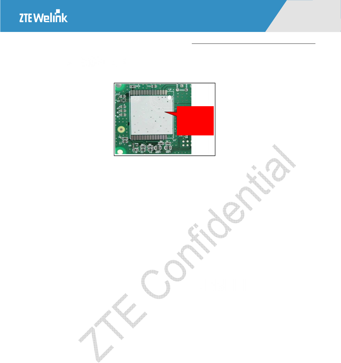
Hardware Development Guide of Module Products
All Rights reserved, No Spreading abroad without Permission of ZTEWelink 60
MW3650
0
Figure 9-1 Green oil and white oil at module’s position on main board
(The figure is just for reference; it doesn’t represent the actual module encapsulation)
In addition, do not lay out other components within 2mm around the module’s position on main board
to ensure the maintenance of the module.
9.3 Module Planeness Standard
The module’s planeness is required to be 0.15mm. Measurement method: put the module on the marble
plane, use the feeler gage to measure the gap width at the position of maximum warp, and do not exert
force on the module during the measurement.
9.3.1 Process Routing Selection
The modules are manufactured with the lead-free process and meet the ROHS requirements, therefore
it’s recommended to follow the lead-free manufacturing process upon the selection of process routing
for module board and main board.
9.3.2 Solder Paste Selection
The solder pastes with metal particle TYPE3 and TYPE4 can fulfill the welding requirements. It is
accordingly recommended to use the no-clean solder paste. If the solder paste which needs cleaning is
used, we cannot guarantee the components on the module board could withstand the washing of the
cleaning solvents. This might cause the functional problems of such components and affect the
appearance of the module. During the printing process, make sure the solder paste’s thickness at the
position of module’s PAD is within 0.18mm -0.20mm.
The white
oil need be
removed
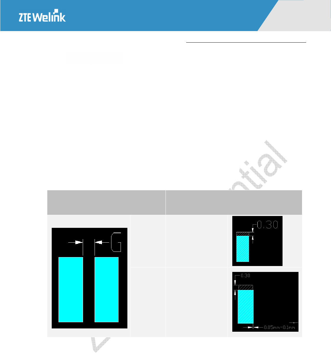
Hardware Development Guide of Module Products
All Rights reserved, No Spreading abroad without Permission of ZTEWelink 61
MW3650
0
9.3.3 Design of module PAD’s steel mesh opening on main board
The thickness of the steel mesh on main board is selected according to the encapsulation type of
components on the main board. Pay attention to the following requirements:
1) Make sure to design the module PAD on main board according to the third item as below.
2) The thickness of steel mesh is 0.15mm or 0.18mm, but the thickness at the position of module pad
can be increased to 0.18~0.20mm or the thickness of steel mesh is directly 0.18mm~0.20mm on
main board.
3) Requirements on the thickness of solder paste: control the thickness between 0.15mm and 0.18mm.
4) See the LCC module PAD’s steel mesh opening in the following table:
Table 9-2 LCC module PAD’s steel mesh opening
Module PAD GAP (G)=Center Distance (e)-
PAD width (X) Steel mesh opening
G≥0.5mm
Drill holes at 100%
scale in the direction of
width;
extend 0.3mm outward
in the direction of
length
G<0.5mm
Contract 0.05~0.1mm
in the direction of
width;
Contract 0.05~0.1mm
inward in the direction
of length, extend
0.5mm outward in the
direction of length.
Hardware Development Guide of Module Products
All Rights reserved, No Spreading abroad without Permission of ZTEWelink 62
MW3650
0
Figure 9-2 Module Board’s Steel Mesh Diagram
9.3.4 Module Board’s SMT process
1)
SMT Pallets:
The pallets, which are suitable for SMT, have been made for most ZTE modules. If the module has
provided the pallets itself and meets the SMT requirements, customers can directly use it for module
SMT.
Figure 9-3 Material Module Pallet
(The figure is just for reference; it doesn’t represent the actual Material Module Pallet)
Otherwise, customers need make a loading tool similar to the pallet. Customers can take out the module
from the packaging box, put them into the pallet according to the sequence and direction, and then start
SMT.
2)
Mounting Pressure:
0.1mm 0.1mm
0.5mm
0.1mm
Steel
mesh
opening
Module PAD on
PCB

Hardware Development Guide of Module Products
All Rights reserved, No Spreading abroad without Permission of ZTEWelink 63
MW3650
0
In order to ensure a good contact between the module and the solder paste on main board, the pressure
of placing the module board on main board should be 2-5N according to our experiences. Different
modules have different numbers of pads, therefore the pressure selected are different. Customers can
select proper pressure based on their own situations to suppress the module paste as little as possible, in
order to avoid the surface tension of the solder paste melts too much to drag the module during reflow.
9.3.5 Module Soldering Reflow Curve
Module soldering furnace temperature curve is:
Peak value: 245+0/-5℃
≥217℃: 30~~60S
150~200 : 60℃~~120S
Temperature rise slope: <3 /S℃
Temperature drop rate: -2~-4 /S℃
Figure 9-4 Module Furnace Temperature Curve Diagram
Hardware Development Guide of Module Products
All Rights reserved, No Spreading abroad without Permission of ZTEWelink 64
MW3650
0
Note: The test board of furnace temperature must be the main board with the module board mounted
on, and there must be testing points at the position of module board.
9.3.6 Reflow method
If the main board used by customers is a double-sided board, it is recommended to mount the module
board at the second time. In addition, it is preferable for the main board to reflow on the mesh belt
when mounting at the first time and the second time. If such failure is caused by any special reason, the
fixture should be also used to make such main board reflow on the track so as to avoid the deformation
of PCB during the reflow process.
9.3.7 Maintenance of defects
If poor welding occurs to the module board and main board, e.g., pseudo soldering of the module board
and main board, the welder can directly use the soldering iron to repair welding according to the
factory’s normal welding parameters.
9.4 Module’s Baking Requirements
The module must be baked prior to the second reflow.
9.4.1 Module’s Baking Environment
The operators must wear dust-free finger cots and anti-static wrist strap under the lead-free and good
static-resistant environment. Refer to the following environment requirements:
The product’s transportation, storage and processing must conform to IPC/JEDEC J-STD-033.

Hardware Development Guide of Module Products
All Rights reserved, No Spreading abroad without Permission of ZTEWelink 65
MW3650
0
9.4.2 Baking device and operation procedure
Baking device: any oven where the temperature can rise up to 125°C or above.
Precautions regarding baking: during the baking process, the modules should be put in the
high-temperature resistant pallet flatly and slightly to avoid the collisions and frictions between the
modules. During the baking process, do not overlay the modules directly because it might cause
damage to the module’s chipset.
9.4.3 Module Baking Conditions
See the baking parameters in Table 9-1.

Hardware Development Guide of Module Products
All Rights reserved, No Spreading abroad without Permission of ZTEWelink 66
MW3650
0
10
Safety Warnings and Notes
During the process of the module secondary development, use and repair, all the safety warnings and notes in this
section should be followed. The module integrator must pass the following safety information to users and operators
or integrate the information into product operating manual:
When RF devices including the module are used, the electronic devices whose shielding performance is not good
may be interfered. Please keep far away from ordinary telephones, televisions, radios and places of office
automatic, to avoid interaction with the module.
Please consult the product manufacturer before the devices containing the module is used beside medical
equipment such as hearing-aid, cochlear implant and heart pacemaker.
Please do not use the devices containing the module in the environment which has potential explosion hazard
such as oil depot and chemical plant and which has special requirements such as hospital and airport.
Please do not expose the module to the strong sunshine to avoid being excessive heated and damaged.
The module does not have waterproof performance, so please avoid liquid entering the module. Please do not use
it in the high humidity environment such as the bathroom to avoid being damaged.
Non-professionals please do not detach the module to avoid people and devices been injured or damaged.
When cleaning the module, please shut down it first and use clean antistatic fabric.
Users have responsibility to follow the relevant regulations and specific operating environment regulations about
wireless communication module and equipment. Our company is not responsible for the relevant loss since the
customer do not follow the rules.
Hardware Development Guide of Module Products
All Rights reserved, No Spreading abroad without Permission of ZTEWelink 67
MW3650
0
Federal Communication Commission
Interference Statement
This device complies with Part 15 of the FCC Rules. Operation is subject to the following two conditions: (1) This
device may not cause harmful interference, and (2) this device must accept any interference received, including
interference that may cause undesired operation.
This equipment has been tested and found to comply with the limits for a Class B digital device, pursuant to Part 15 of
the FCC Rules. These limits are designed to provide reasonable protection against harmful interference in a residential
installation. This equipment generates, uses and can radiate radio frequency energy and, if not installed and used in
accordance with the instructions, may cause harmful interference to radio communications. However, there is no
guarantee that interference will not occur in a particular installation. If this equipment does cause harmful interference
to radio or television reception, which can be determined by turning the equipment off and on, the user is encouraged
to try to correct the interference by one of the following measures:
● Reorient or relocate the receiving antenna.
● Increase the separation between the equipment and receiver.
● Connect the equipment into an outlet on a circuit different from that to which the receiver is connected.
● Consult the dealer or an experienced radio/TV technician for help.
FCC Caution:
Any changes or modifications not expressly approved by the party responsible for compliance could void the user's
authority to operate this equipment.
This transmitter must not be co-located or operating in conjunction with any other antenna or transmitter.
Radiation Exposure Statement:
This equipment complies with FCC radiation exposure limits set forth for an uncontrolled environment. This
equipment should be installed and operated with minimum distance 20cm between the radiator & your body.
This device is intended only for OEM integrators under the following conditions:
1) The antenna must be installed such that 20 cm is maintained between the antenna and
users, and the maximum antenna gain allowed for use with this device is 1.6dBi.
2) The transmitter module may not be co-located with any other transmitter or antenna.
Hardware Development Guide of Module Products
All Rights reserved, No Spreading abroad without Permission of ZTEWelink 68
MW3650
0
As long as 2 conditions above are met, further transmitter test will not be required. However, the
OEM integrator is still responsible for testing their end-product for any additional compliance
requirements required with this module installed
IMPORTANT NOTE: In the event that these conditions can not be met (for example certain laptop
configurations or co-location with another transmitter), then the FCC authorization is no longer
considered valid and the FCC ID can not be used on the final product. In these circumstances, the
OEM integrator will be responsible for re-evaluating the end product (including the transmitter)
and obtaining a separate FCC authorization.
End Product Labeling
This transmitter module is authorized only for use in device where the antenna may be installed
such that 20 cm may be maintained between the antenna and users. The final end product must
be labeled in a visible area with the following: “Contains FCC ID:SRQ-MW3650”. The grantee's
FCC ID can be used only when all FCC compliance requirements are met.
Manual Information To the End User
The OEM integrator has to be aware not to provide information to the end user regarding how to
install or remove this RF module in the user’s manual of the end product which integrates this
module. The end user manual shall include all required regulatory information/warning as show
in this manual.