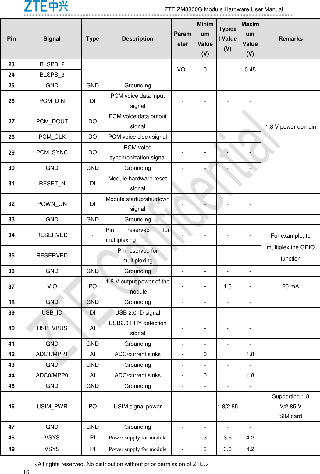
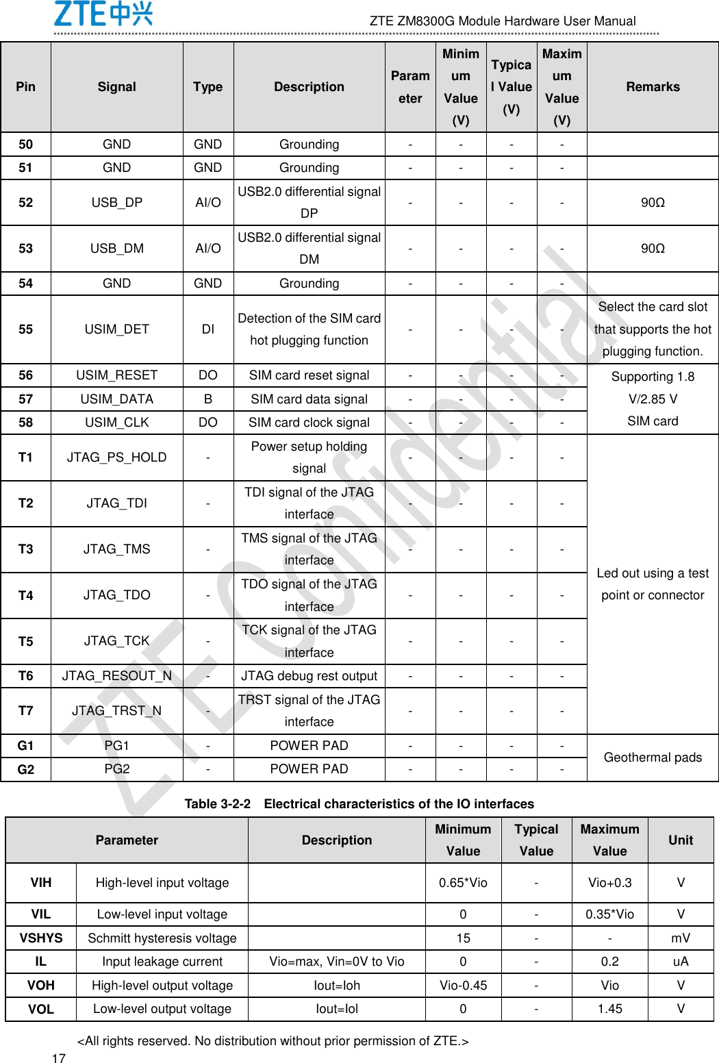
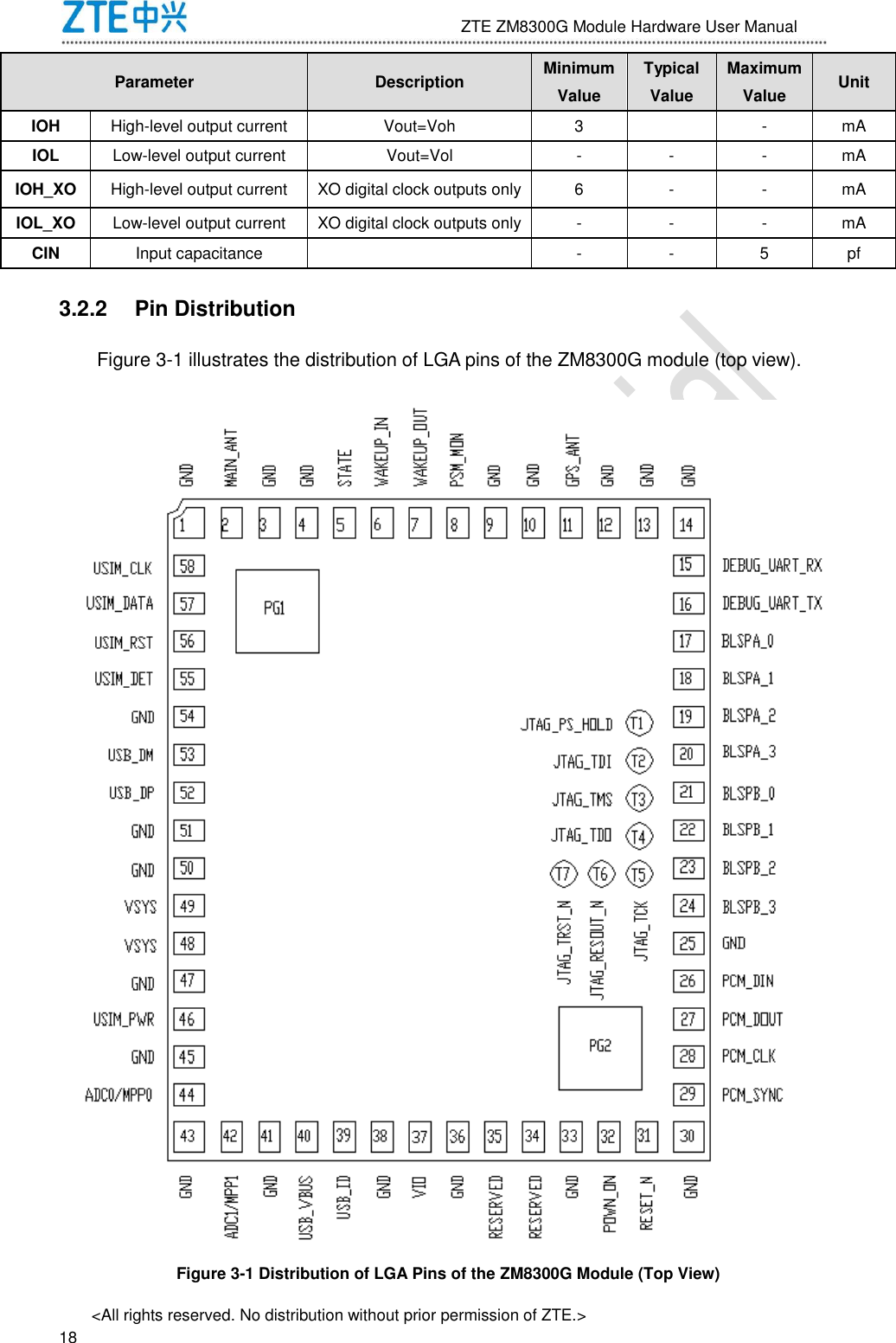
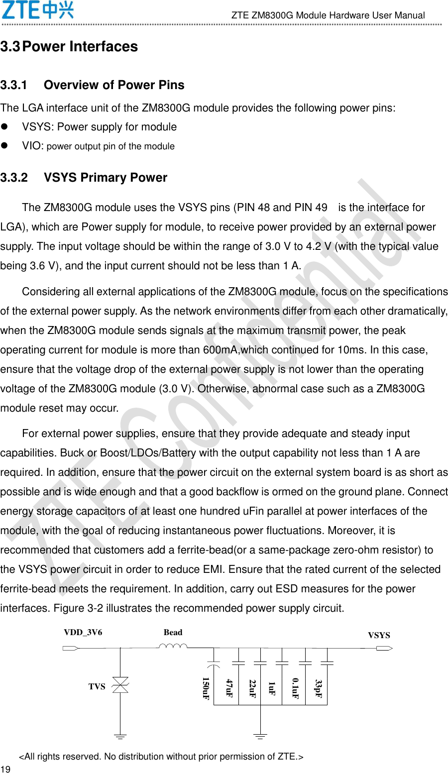
ZTE ZM8300G NB-IoT/eMTC Module User Manual
ZTE Corporation NB-IoT/eMTC Module Users Manual
UserManual.wiki
>
ZTE
>
ZM8300G User Manual
Users Manual
Navigation menu
Upload a User Manual
Namespaces
Wiki Guide
HTML
PDF
Info
Views
User Manual
Discussion / Help
Navigation
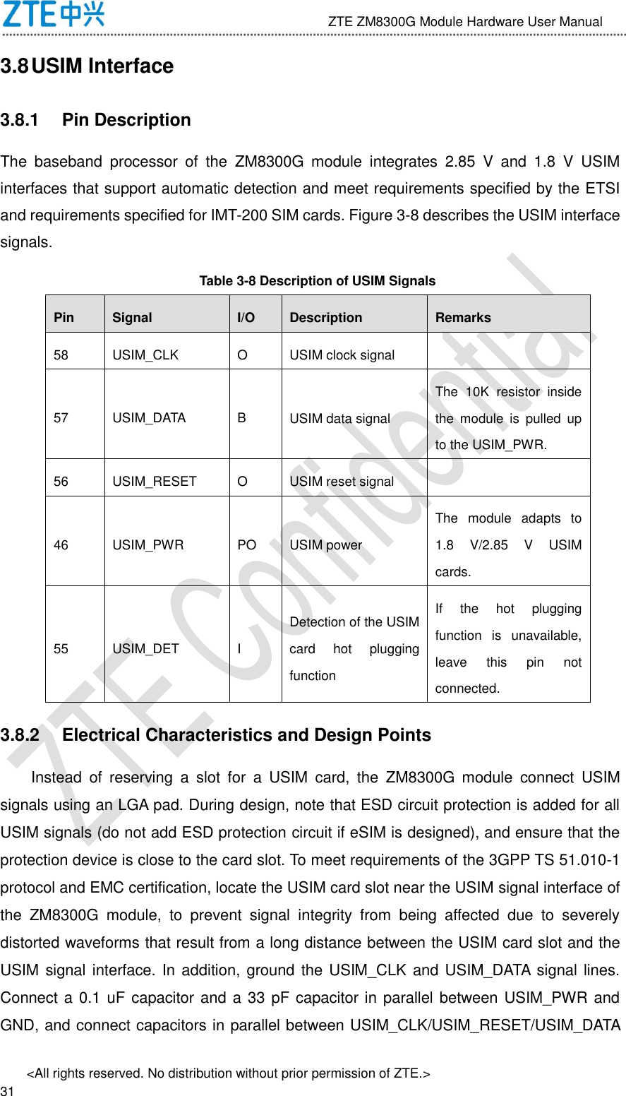
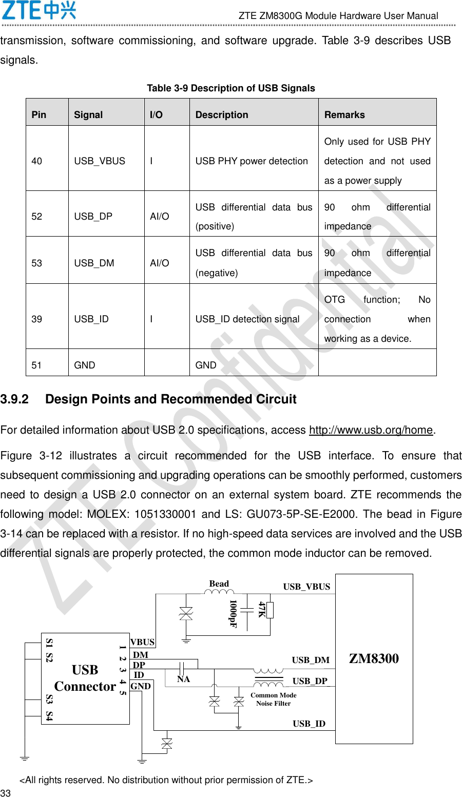
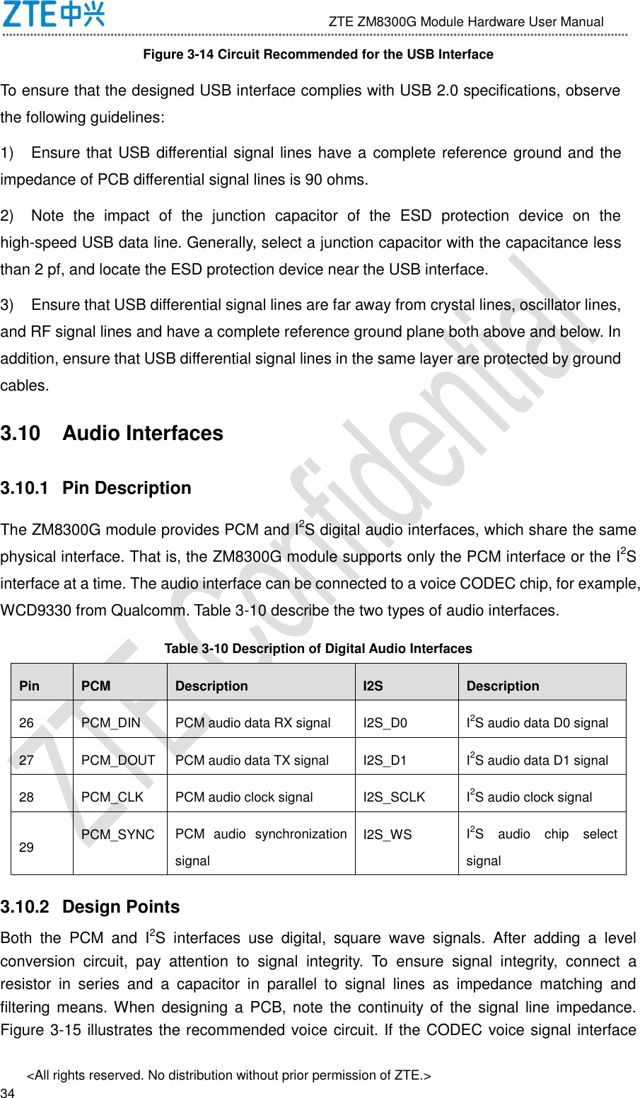
![ZTE ZM8300G Module Hardware User Manual <All rights reserved. No distribution without prior permission of ZTE.> 32 and GND, with the goal of filtering out interference from RF signals. Then, connect a zero-ohm resistor in series to the USIM_DATA, USIM_CLK, and USIM_RESET signal lines as a measure reserved for ESD protection and EMI design.If the hot plug for SIM is applied, contact ZTE FAE team. 3.8.3 Circuit Recommended for the USIM Card Interface Figure 3-13 illustrates the peripheral circuit recommended for the USIM card interface. USIMSlotsw c7 c6 c5 c3 c2 c1GND[0~9]USIM_PWRUSIM_RESETUSIM_CLKUSIM_DATAUSIM_DETVIO33pF0.1uF0Ω0Ω0Ω1KΩNANANANA12345USIM1_DATAUSIM_PWRUSIM1_RESETUSIM1_CLKOvervoltage ProtectorsUSIM1_RESETUSIM1_CLKUSIM1_DATA Figure 3-13Peripheral Circuit Recommended for the USIM Card Interface In addition to the method of designing a USIM card slot on the system board, customers can design an eSIM chip. The ST or Gemalto scheme is recommended. 3.9 USB Interface 3.9.1 Pin Description The ZM8300G module provides an integrated USB transceiver, which complies with USB2.0 and supports the high speed mode (480 Mbit/s), full speed mode (12 Mbit/s), and low speed mode (1.5 Mbit/s). The USB interface primarily applies to AT commands, data](https://usermanual.wiki/ZTE/ZM8300G/User-Guide-3638367-Page-33.png)