Users Manual

ZTE ZM8300G Module Hardware User Manual
<All rights reserved. No distribution without prior permission of ZTE.>
ZTE ZM8300G Module
Hardware User Manual
Product Model: ZM8300G IoT Module
Document Version: 1.3
Publishing Date: 2017-06-20

ZTE ZM8300G Module Hardware User Manual
<All rights reserved. No distribution without prior permission of ZTE.>
LEGAL INFORMATION
By accepting this certain document of ZTE CORPORATION you agree to the following
terms. If you do not agree to the following terms, please notice that you are not allowed to
use this document.
Copyright © 2017 ZTE CORPORATION. Any rights not expressly granted herein are
reserved. This document contains proprietary information of ZTE CORPORATION. Any
reproduction, transfer, distribution, use or disclosure of this document or any portion of this
document, in any form by any means, without the prior written consent of ZTE
CORPORATION is prohibited.
and are registered trademarks of ZTE CORPORATION. ZTE’s
company name, logo and product names referenced herein are either trademarks or
registered trademarks of ZTE CORPORATION. Other product and company names
mentioned herein may be trademarks or trade names of their respective owners. Without
the prior written consent of ZTE CORPORATION or the third party owner thereof,
anyone’s access to this document should not be construed as granting, by implication,
estopped or otherwise, any license or right to use any marks appearing in the document.
The design of this product complies with requirements of environmental protection and
personal security. This product shall be stored, used or discarded in accordance with
product manual, relevant contract or laws and regulations in relevant country (countries).
This document is provided “as is” and “as available”. Information contained in this
document is subject to continuous update without further notice due to improvement and
update of ZTE CORPORATION’s products and technologies.
ZTE CORPORATION
Address:
NO. 55
Hi-tech Road South
ShenZhen
P.R.China
518057
Website:
http://www.zte.com.cn
ZTE ZM8300G Module Hardware User Manual
<All rights reserved. No distribution without prior permission of ZTE.>
Revision History
Product Version
Document
Version
Reason for Revision
Revision Date
ZM8300G IoT Module
Hardware User
Manual
V1.0
First edition
2017.03.01
ZM8300G IoT Module
Hardware User Manual
V1.1
1. Updated the operating voltage,
temperature range, and partial
test data of the ZM8300G
module.
2. Updated the Power on/off time
of the ZM8300G module.
3. Updated the hardware reset
procedure of the ZM8300G
module.
4. Change the pin PIN34/35 to
multiplex reserved function.
5. Updated the PSM function and
added the active pown_on
function.
6. Added information to the RF
and antenna design sections.
7. Fixed font and formatting
bugs.
2017.04.13
ZM8300G IoT Module
Hardware User Manual
V1.2
1. Added remarks for pown_on
scheme 3 to section 3.4.2.
2. Added precautions to section
3.4.4.
3. Added default configurations
of serial ports to section 3.6.2.
4. Added the following
information to Table 3-8: If the hot
plugging function is unavailable,
leave the UIM_DET pin not
connected.
2017.05.04
ZTE ZM8300G Module Hardware User Manual
<All rights reserved. No distribution without prior permission of ZTE.>
Product Version
Document
Version
Reason for Revision
Revision Date
5. Added precautions for MPP
indicator lighting to section
3.11.1.
6. Added information about
peripheral components in the
circuit recommended for an
antenna to section 3.13.2.
ZM8300G IoT module
hardware manual
V1.3
1.added section 2.6
2.Update section 3.4.2 for
module power of requirement
3.Update section 3.4.2 for
module hard reset requirement
4.Update section 3.4.4/5/6/ for
module waking up,state
indication,PSM_MON
5.Update section 3.6 for
description of UART
6.Update table 4-2,4-3,4-4 for
parameter
2017.06.20

ZTE ZM8300G Module Hardware User Manual
<All rights reserved. No distribution without prior permission of ZTE.>
Contents
1 OVERVIEW ............................................................................................................................... 7
1.1 SCOPE ...................................................................................................................................... 7
1.2 ACRONYMS ............................................................................................................................... 7
1.3 PRODUCT DESCRIPTION ............................................................................................................... 7
2 GENERAL INTRODUCTION ........................................................................................................ 9
2.1 ABOUT THIS CHAPTER ................................................................................................................. 9
2.2 FEATURE INTRODUCTION .............................................................................................................. 9
2.3 APPLICATION DIAGRAM ............................................................................................................. 11
2.4 CIRCUIT DIAGRAM .................................................................................................................... 11
2.5 OUTLINE DIMENSIONS DIAGRAM ................................................................................................. 12
2.6 TRANSFERRED BOARD AND DEBUG BOARD ............................................................................................. 13
3 APPLICATION INTERFACES ...................................................................................................... 14
3.1 ABOUT THIS CHAPTER ............................................................................................................... 14
3.2 DEFINITIONS OF LGA PINS ......................................................................................................... 14
3.2.1 Pin Definitions ............................................................................................................. 14
3.2.2 Pin Distribution ............................................................................................................ 18
3.3 POWER INTERFACES .................................................................................................................. 19
3.3.1 Overview of Power Pins ............................................................................................... 19
3.3.2 VSYS Primary Power .................................................................................................... 19
3.3.3 VIO Power .................................................................................................................... 20
3.4 CONTROL SIGNAL INTERFACES ..................................................................................................... 20
3.4.1 Overview of Control Signals ........................................................................................ 20
3.4.2 POWN_ON Signal ........................................................................................................ 20
3.4.3 RESET_N Signal ........................................................................................................... 22
3.4.4 WAKEUP_IN Signal ...................................................................................................... 23
3.4.5 WAKEUP_OUT Signal .................................................................................................. 24
3.4.6 PSM_MON Signal ........................................................................................................ 24
3.4.7 STATE Signal ................................................................................................................ 25
3.5 DEBUG_UART INTERFACE........................................................................................................ 25
3.6 BLSP INTERFACES ..................................................................................................................... 26
3.6.1 Pin Description ............................................................................................................ 26
3.6.2 UART Interfaces ........................................................................................................... 26
3.6.3 SPI Bus Interface .......................................................................................................... 27

ZTE ZM8300G Module Hardware User Manual
<All rights reserved. No distribution without prior permission of ZTE.>
3.6.4 I2C Bus ......................................................................................................................... 29
3.7 GPIO INTERFACES .................................................................................................................... 30
3.8 USIM INTERFACE ..................................................................................................................... 31
3.8.1 Pin Description ............................................................................................................ 31
3.8.2 Electrical Characteristics and Design Points ................................................................ 31
3.8.3 Circuit Recommended for the USIM Card Interface..................................................... 32
3.9 USB INTERFACE ....................................................................................................................... 32
3.9.1 Pin Description ............................................................................................................ 32
3.9.2 Design Points and Recommended Circuit .................................................................... 33
3.10 AUDIO INTERFACES ................................................................................................................... 34
3.10.1 Pin Description ............................................................................................................ 34
3.10.2 Design Points ............................................................................................................... 34
3.11 ADC/MPP INTERFACES ............................................................................................................. 35
3.11.1 Pin Description ............................................................................................................ 35
3.11.2 Design Points ............................................................................................................... 35
3.12 JTAG INTERFACE ...................................................................................................................... 36
3.12.1 Pin Description ............................................................................................................ 36
3.12.2 Design Points ............................................................................................................... 37
3.13 ANTENNA INTERFACES ............................................................................................................... 37
3.13.1 Pin Description ............................................................................................................ 37
3.13.2 Antenna Design Points ................................................................................................ 38
4 RF CHARACTERISTICS ............................................................................................................. 39
4.1 ABOUT THIS CHAPTER ............................................................................................................... 39
4.1.1 Power Supply ............................................................................................................... 39
4.1.2 Operating Current ....................................................................................................... 39
4.2 REFERENCE DESIGN FOR RF LAYOUT ............................................................................................. 39
4.3 TEST STANDARD FOR CONDUCTED RF ........................................................................................... 40
4.4 REQUIREMENTS FOR ANTENNA DESIGN......................................................................................... 40
4.4.1 Key Points for Antenna Design .................................................................................... 40
4.4.2 Antenna Efficiency ....................................................................................................... 41
4.4.3 VSWR ........................................................................................................................... 42
4.4.4 S11 ............................................................................................................................... 42
4.4.5 Polarization ................................................................................................................. 42
4.4.6 Radiation Pattern ........................................................................................................ 42
4.4.7 Requirements for IoT Antenna Design ......................................................................... 43
4.4.8 Precautions for Early Antenna Design ......................................................................... 43

ZTE ZM8300G Module Hardware User Manual
<All rights reserved. No distribution without prior permission of ZTE.>
5 MECHANICAL CHARACTERISTICS ............................................................................................ 44
5.1 ABOUT THIS CHAPTER ............................................................................................................... 44
5.2 ASSEMBLY PROCEDURE .............................................................................................................. 44
5.2.1 Overview ..................................................................................................................... 44
5.2.2 Steel Mesh ................................................................................................................... 44
5.2.3 Reflow Curve ............................................................................................................... 46
5.3 REPAIR PROCEDURE .................................................................................................................. 47
5.3.1 Repair Procedure ......................................................................................................... 47
5.3.2 Module Dismantling .................................................................................................... 47
5.3.3 treatment in weld area ............................................................................................... 47
5.3.4 Module Installation ..................................................................................................... 47
5.3.5 Visual Inspection ......................................................................................................... 47
5.3.6 Feature Validation ....................................................................................................... 47
5.4 EMC AND ESD PROTECTION ...................................................................................................... 48
ZTE ZM8300G Module Hardware User Manual
<All rights reserved. No distribution without prior permission of ZTE.>
7
1 Overview
1.1 Scope
This document is intended for customers who use and develop wireless IoT terminal products.
This document provides information and precautions for developing the hardware of IoT
terminal products using ZTE ZM8300G IoT wireless module. This document applies only to
hardware development that uses the ZM8300G IoT wireless module.
1.2 Acronyms
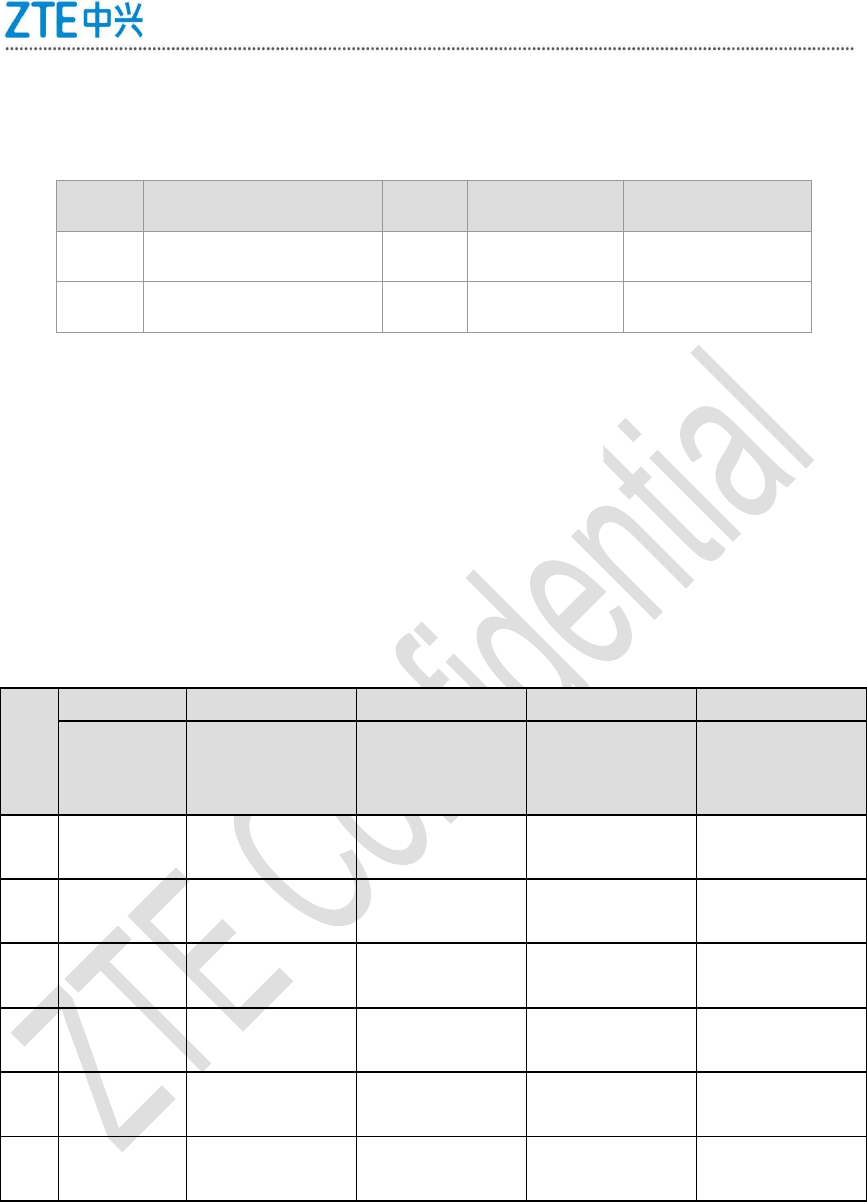
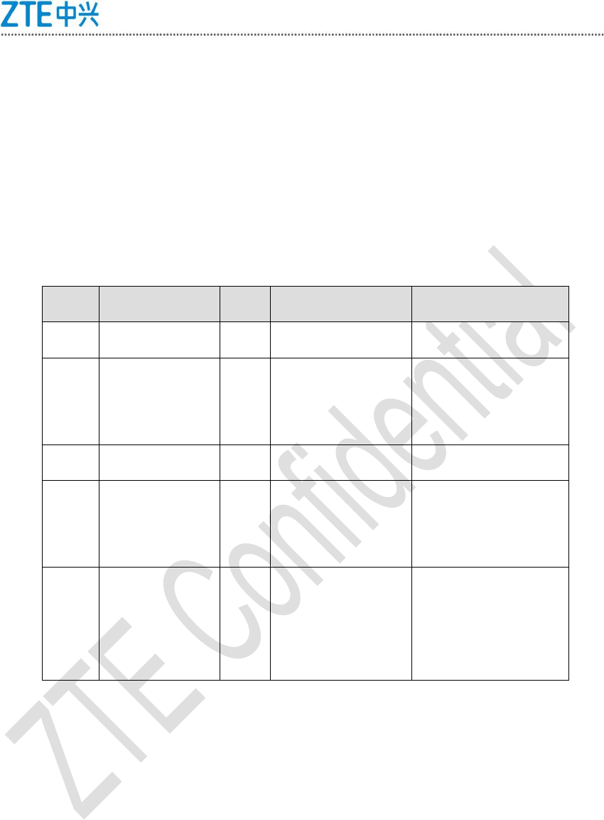
Table 1-1 Acronyms Used in This Document
Acronym
Full Name
ESD
Electro-Static discharge
USB
Universal Serial Bus
UART
Universal Asynchronous Receiver Transmitter
USIM
Universal Subscriber Identity Module
I/O
Input/Output
BLSP
BAM (bus access module) low-speed peripheral
SPI
Serial Peripheral Interface
I2C
Inter-Integrated Circuit
PCM
Pulse-coded Modulation
LED
Light Emitting Diode
GPIO
General-purpose input/output
EMC
Electromagnetic Compatibility
NB-IoT
Narrow Band Internet of Things
AP
Application processor
1.3 Product Description
The ZM8300G module is an IoT module that uses the LGA packaging. The ZM8300G module
supports the CAT NB/eMTC, multiple band combinations such as Band 5/8 and Band 3/39,

ZTE ZM8300G Module Hardware User Manual
<All rights reserved. No distribution without prior permission of ZTE.>
8
and Support for GNSS (GPS, Beidou, GLONASS, and Galileo), and provides a wide variety
of interfaces, such as the USB, UART, SPI, I2C, PCM, and ADC. The ZM8300G module can
be used for the development of various kinds of IoT products. This document describes the
functions, application interfaces, RF characteristics, electrical characteristics, reliability, and
mechanical characteristics of the ZM8300G module and provides precautions for design, with
the goal of providing design guidelines and references for the hardware application and
development of the ZM8300G module.
The ZM8300G module is small and its dimensions are as follows: 23.0 mm x 28.0 mm x 2.4
mm (excluding the label thickness, which is 0.1 mm). The ZM8300G module meets
requirements of M2M applications and can be widely used in IoT-related devices such as data
metering devices, data collection devices, security solution devices, wireless POS devices,
and mobile computing devices.
Being an LGA module, the ZM8300G IoT module provides 67 pads (consisting of 58 LGA
signal pads, seven JTAG test pads, and two PG pads) and can be applied to customers'
design.
ZTE ZM8300G Module Hardware User Manual
<All rights reserved. No distribution without prior permission of ZTE.>
9
2 General Introduction
2.1 About This Chapter
This chapter describes the ZM8300G module in general, covering the following aspects:
Feature introduction
Application diagram
Circuit diagram
Outline dimensions diagram
2.2 Feature Introduction
Table 2-1 provides major technical parameters and features of the ZM8300G module.
Table 2-1 Major Technical Parameters and Features of the ZM8300G Module
Title
Description
Physical features
Dimensions: 23.0 mm x 28.0 mm x 2.4 mm
Weight: 3.3 g
Airlink
technologies
Supports the NB-IoT: Band 5/8,3/39.
Supports the GNSSes: GPS, Beidou, GLONASS, and Galileo.
Operating
temperature
-40 to 85℃
Storage
temperature
-40 to 85℃
Operating voltage
DC 3.0 V to 4.2 V (with the typical value being 3.6 V)
AT command set
Refer to the ZTE ZM8300G IoT Module AT Command Set.
Power
consumption (3.6
V)
leakage current: 4.8 uA
PSM (power saving mode) sleep current: 7 uA
Average sleep current: 0.7 mA
Idle current:1.47mA , 2.56s DRX Online ◆注 1 idle current: note 1
Average operating current:
NB-IoT: 50 mA (UL)/50 mA (DL) ◆Note 2
ZTE ZM8300G Module Hardware User Manual
<All rights reserved. No distribution without prior permission of ZTE.>
10
Title
Description
eMTC: 115 mA (UL)/112 mA (DL) ◆Note 3
Application
interfaces (LGA
interfaces)
USB 2.0 interface
USIM card interface (2.85 V and 1.8 V), supporting hot plugging
UART/JTAG debug interface
UART/SPI/I2C/GPIO (multiple combinations; for details, see Table 3-6
PCM/I2S interface
ADC/MPP interface
Startup/Shutdown interface
Module hardware reset interface
Status indication interface
AP waking up interface for module
Module waking up interface for AP
Antenna interface
Antenna pads (1xeMTC/NB-IoT antenna pad; 1xGPS antenna pad)
◆Note 1: The lab data(sleep and Idle current) provided by Qualcomm ‘s test data from lab.
◆Note 2: The lab data provided by Qualcomm ‘s test data from lab. The operating condition is as
follows: LTE 10 MHz bandwidth embedded data call@0dBm TX, UL/DL only. Used data packets are
as follows: UL 62.5 kbps (15 kHz single tone)/DL 21 kbps (multi tone).
◆Note 3: The lab data provided by Qualcomm ‘s test data from lab. The operating condition is as
follows: LTE 10 MHz bandwidth embedded data call@0dBm TX, UL/DL only. 375 kbps data packets
are used in both the uplink and downlink directions.
ZTE ZM8300G Module Hardware User Manual
<All rights reserved. No distribution without prior permission of ZTE.>
11
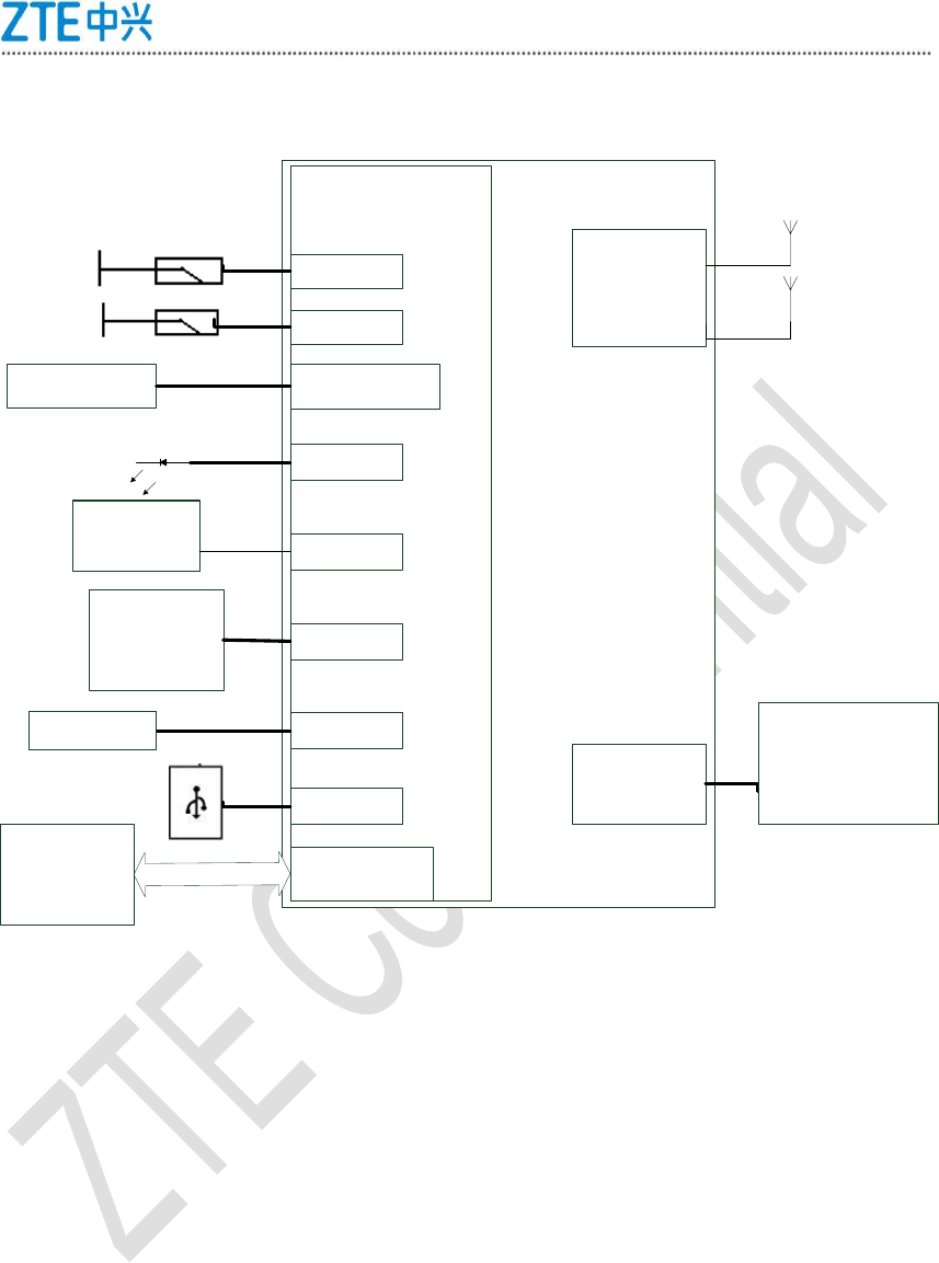
2.3 Application Diagram
ZM8300 IoT
Application
interface
POWER
ANT
WAKEUP-IN/OUT
POWN_ON
RESET_N
WAKEUP-IN/OUT
STATE
PCM
USIM
CODEC
USB
MAIN ANT
GPS ANT
UART/SPI/I2C/
GPIO
IC
LED
ADC/MPPADC/LED 3.0V~4.2V
Typical
3.6V
USIM SLOT
Or
eSIM
Figure 2-1 Application Diagram of the ZM8300G Module
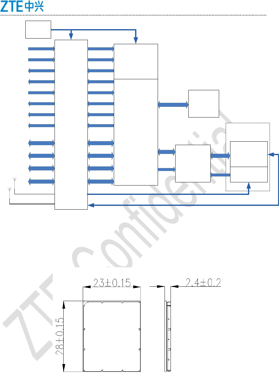
2.4 Circuit Diagram
Figure 2-2 is the circuit diagram of the ZM8300G module. The ZM8300G module consists
of the following main function units:
Baseband controller/power management unit
Memory (1 Gbit NAND + 512 bit LPDDR2)
LGA interface unit
RF transceiver IC
RF front-end circuit
ZTE ZM8300G Module Hardware User Manual
<All rights reserved. No distribution without prior permission of ZTE.>
12
CPU
PMU
LGA
Interface
MCP
FLASH
RF
transceiver
RF TRx
GPS Rx
RF_
RX/TX
GPS_RX
RF Front-end
RX/TX
CONTROL
VSYS
VIO
Power
supply
GPS_ANT
MAIN_ANT
USIM
UATR/SPI
/I2C
WAKEUP_IN
WAKEUP_OUT
WAKEUP_IN
STATUS
USB
PSM_MON
RESET_N
JTAG/UART
ZM8300 IoT
ADC/MPP ADC/MPP
POWN_ON
JTAG/Debug_UART
USIM/eSIM
USB
UATR/SPI
/I2C
STATUS
PSM_MON
WAKEUP_OUT
VIO
RESET_N
POWN_ON
Figure 2-1 Circuit Diagram of the ZM8300G Module
2.5 Outline Dimensions Diagram
Figure 2-3 Dimensions of the ZM8300G Module (in mm)
ZTE ZM8300G Module Hardware User Manual
<All rights reserved. No distribution without prior permission of ZTE.>
13
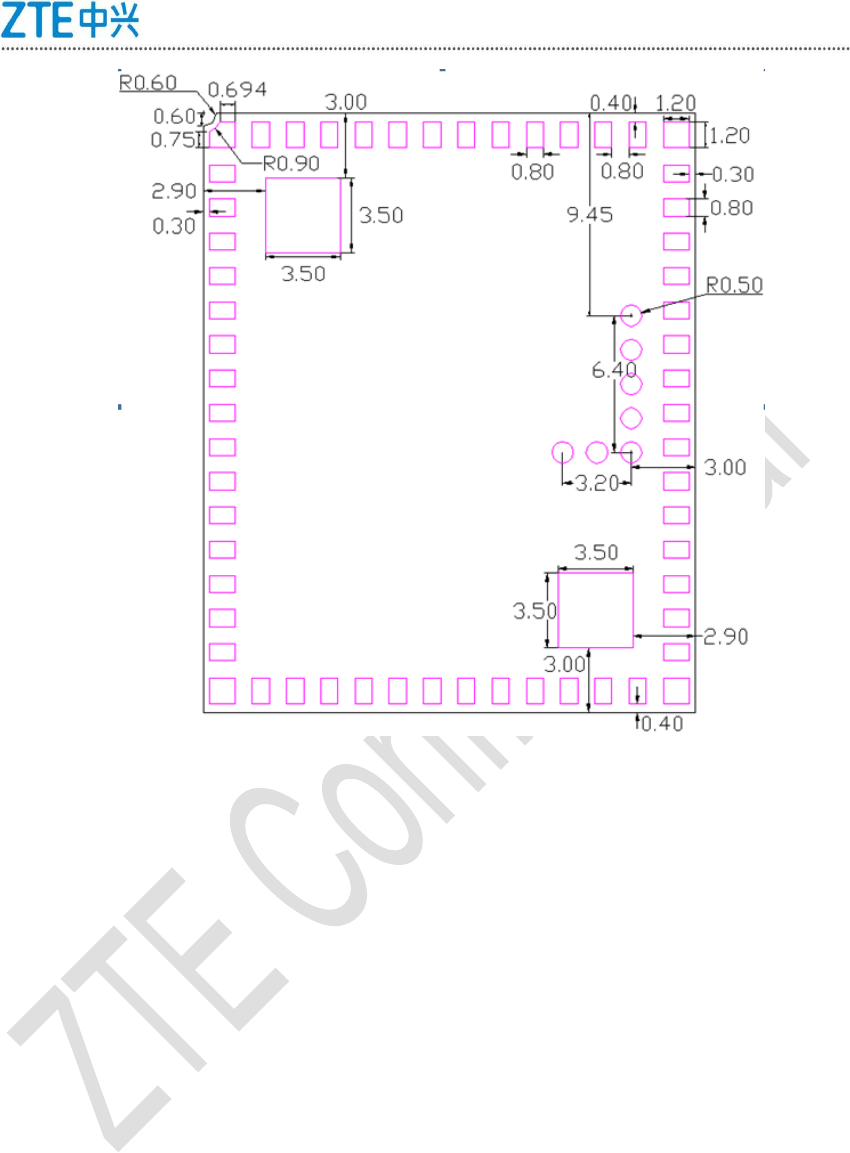
Figure 2-4 Dimensions of the BOT Side of the ZM8300G Module (in mm) ◆Note 4
◆Note 4: Figure 2-4 is the outline pad diagram of the ZM8300G module. If pad design of a
system board is required, ZTE can provide a dedicated outline drawing file.
2.6 transferred board and debug board
ZTE provide transferred board,debug board and peripheral such as antenna,power
supplier,Serial Interface cable in order to better apply the ZM8300G to design the product for
you,detailed referred to <<ZTE debug board use manual for module product>>
ZTE ZM8300G Module Hardware User Manual
<All rights reserved. No distribution without prior permission of ZTE.>
14
3 Application Interfaces
3.1 About This Chapter
This chapter describes the following major interfaces provided by the ZM8300G module:
Power interfaces
Control signal interfaces
DEBUG_UART interface
BLSP interfaces
GPIO interfaces
USIM interface
USB interface
Audio interfaces
ADC/MPP interfaces
JTAG interface
Antenna interfaces
3.2 Definitions of LGA Pins
The ZM8300G IoT module uses the LGA package and has 67 pads, namely, 58 signal pads,
seven JTAG test pads, and two PG pads. Using the pads, the ZM8300G module is connected
to a customer's IoT application platform. The following sections describe interfaces provided
by the ZM8300G module.
3.2.1 Pin Definitions
Table 3-1 provides definitions for input/output parameters of pins of the ZM8300G module.
Table 3-1 Definitions for Input/Output Parameters of Pins of the ZM8300G Module ◆Note 1
Type
Description
DO
Digital output
DI
Digital input
B
Bidirectional digital
PI
Power input
PO
Power output
I
In
ZTE ZM8300G Module Hardware User Manual
<All rights reserved. No distribution without prior permission of ZTE.>
15
O
Out
AI
Analog input
AO
Analog output
◆Note 1: The pin directions in Table 3-1 are based on the body of the ZM8300G module.
Table 3-2 provides definitions for pins of the ZM8300G LGA module.
Table 3-2-1 Definitions for Interfaces Provided by the ZM8300G Module
Pin
Signal
Type
Description
Param
eter
Minim
um
Value
(V)
Typica
l Value
(V)
Maxim
um
Value
(V)
Remarks
1
GND
GND
Grounding
-
-
-
-
2
MAIN_ANT
-
Main antenna interface
-
-
-
-
50 Ω
3
GND
GND
Grounding
-
-
-
-
4
GND
GND
Grounding
-
-
-
-
5
STATE
DO
Module status indication
signal
VOH
1
1.8
1.9
1.8 V Power domain
VOL
0
-
0.45
6
WAKEUP_IN
DI
AP waking up module
signal
VIH
1
-
2.1
VIL
0
-
0.63
7
WAKEUP_OUT
DO
module waking up AP
signal
VOH
1
1.8
1.9
VOL
0
-
0.45
8
PSM_MON
DO
Module deep sleeping
indication signa
VOH
1
1.8
1.9
VOL
0
-
0.45
9
GND
GND
Grounding
-
-
-
-
10
GND
GND
Grounding
-
-
-
-
11
GPS_ANT
-
GPS antenna interface
-
-
-
-
50 ohms
12
GND
GND
Grounding
-
-
-
-
13
GND
GND
Grounding
-
-
-
-
14
GND
GND
Grounding
-
-
-
-
15
DEBUG_UART_RX
DI
Debug serial port RX
signal
VIH
-
-
-
Led out by means of
external design
16
DEBUG_UART_TX
DO
Debug serial port TX
signal
VOH
-
-
-
17
BLSPA_0
B
Two groups of four-wire
BLSP signals being
configured as UART,
SPI, I2C, and GPIO
interfaces
VIH
1
-
2.1
1.8 V power domain
18
BLSPA_1
19
BLSPA_2
VIL
0
-
0.63
20
BLSPA_3
21
BLSPB_0
VOH
1
1.8
1.9
22
BLSPB_1
ZTE ZM8300G Module Hardware User Manual
<All rights reserved. No distribution without prior permission of ZTE.>
16
Pin
Signal
Type
Description
Param
eter
Minim
um
Value
(V)
Typica
l Value
(V)
Maxim
um
Value
(V)
Remarks
23
BLSPB_2
VOL
0
-
0.45
24
BLSPB_3
25
GND
GND
Grounding
-
-
-
-
26
PCM_DIN
DI
PCM voice data input
signal
-
-
-
-
1.8 V power domain
27
PCM_DOUT
DO
PCM voice data output
signal
-
-
-
-
28
PCM_CLK
DO
PCM voice clock signal
-
-
-
-
29
PCM_SYNC
DO
PCM voice
synchronization signal
-
-
-
-
30
GND
GND
Grounding
-
-
-
-
31
RESET_N
DI
Module hardware reset
signal
-
-
-
-
32
POWN_ON
DI
Module startup/shutdown
signal
-
-
-
-
33
GND
GND
Grounding
-
-
-
-
34
RESERVED
-
Pin reserved for
multiplexing
-
-
-
-
For example, to
multiplex the GPIO
function
35
RESERVED
-
Pin reserved for
multiplexing
-
-
-
-
36
GND
GND
Grounding
-
-
-
-
37
VIO
PO
1.8 V output power of the
module
-
-
1.8
-
20 mA
38
GND
GND
Grounding
-
-
-
-
39
USB_ID
DI
USB 2.0 ID signal
-
-
-
-
40
USB_VBUS
AI
USB2.0 PHY detection
signal
-
-
-
-
41
GND
GND
Grounding
-
-
-
-
42
ADC1/MPP1
AI
ADC/current sinks
-
0
1.8
43
GND
GND
Grounding
-
-
-
-
44
ADC0/MPP0
AI
ADC/current sinks
-
0
1.8
45
GND
GND
Grounding
-
-
-
-
46
USIM_PWR
PO
USIM signal power
-
-
1.8/2.85
-
Supporting 1.8
V/2.85 V
SIM card
47
GND
GND
Grounding
-
-
-
-
48
VSYS
PI
Power supply for module
-
3
3.6
4.2
49
VSYS
PI
Power supply for module
-
3
3.6
4.2
ZTE ZM8300G Module Hardware User Manual
<All rights reserved. No distribution without prior permission of ZTE.>
17
Pin
Signal
Type
Description
Param
eter
Minim
um
Value
(V)
Typica
l Value
(V)
Maxim
um
Value
(V)
Remarks
50
GND
GND
Grounding
-
-
-
-
51
GND
GND
Grounding
-
-
-
-
52
USB_DP
AI/O
USB2.0 differential signal
DP
-
-
-
-
90Ω
53
USB_DM
AI/O
USB2.0 differential signal
DM
-
-
-
-
90Ω
54
GND
GND
Grounding
-
-
-
-
55
USIM_DET
DI
Detection of the SIM card
hot plugging function
-
-
-
-
Select the card slot
that supports the hot
plugging function.
56
USIM_RESET
DO
SIM card reset signal
-
-
-
-
Supporting 1.8
V/2.85 V
SIM card
57
USIM_DATA
B
SIM card data signal
-
-
-
-
58
USIM_CLK
DO
SIM card clock signal
-
-
-
-
T1
JTAG_PS_HOLD
-
Power setup holding
signal
-
-
-
-
Led out using a test
point or connector
T2
JTAG_TDI
-
TDI signal of the JTAG
interface
-
-
-
-
T3
JTAG_TMS
-
TMS signal of the JTAG
interface
-
-
-
-
T4
JTAG_TDO
-
TDO signal of the JTAG
interface
-
-
-
-
T5
JTAG_TCK
-
TCK signal of the JTAG
interface
-
-
-
-
T6
JTAG_RESOUT_N
-
JTAG debug rest output
-
-
-
-
T7
JTAG_TRST_N
-
TRST signal of the JTAG
interface
-
-
-
-
G1
PG1
-
POWER PAD
-
-
-
-
Geothermal pads
G2
PG2
-
POWER PAD
-
-
-
-
Table 3-2-2 Electrical characteristics of the IO interfaces
Parameter
Description
Minimum
Value
Typical
Value
Maximum
Value
Unit
VIH
High-level input voltage
0.65*Vio
-
Vio+0.3
V
VIL
Low-level input voltage
0
-
0.35*Vio
V
VSHYS
Schmitt hysteresis voltage
15
-
-
mV
IL
Input leakage current
Vio=max, Vin=0V to Vio
0
-
0.2
uA
VOH
High-level output voltage
Iout=Ioh
Vio-0.45
-
Vio
V
VOL
Low-level output voltage
Iout=Iol
0
-
1.45
V
ZTE ZM8300G Module Hardware User Manual
<All rights reserved. No distribution without prior permission of ZTE.>
18
Parameter
Description
Minimum
Value
Typical
Value
Maximum
Value
Unit
IOH
High-level output current
Vout=Voh
3
-
mA
IOL
Low-level output current
Vout=Vol
-
-
-
mA
IOH_XO
High-level output current
XO digital clock outputs only
6
-
-
mA
IOL_XO
Low-level output current
XO digital clock outputs only
-
-
-
mA
CIN
Input capacitance
-
-
5
pf
3.2.2 Pin Distribution
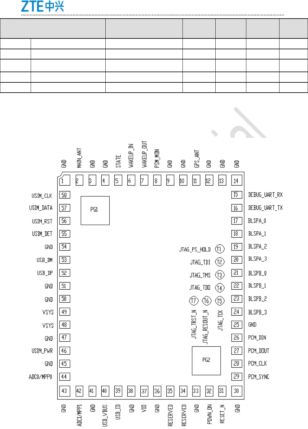
Figure 3-1 illustrates the distribution of LGA pins of the ZM8300G module (top view).
Figure 3-1 Distribution of LGA Pins of the ZM8300G Module (Top View)
ZTE ZM8300G Module Hardware User Manual
<All rights reserved. No distribution without prior permission of ZTE.>
19
3.3 Power Interfaces
3.3.1 Overview of Power Pins
The LGA interface unit of the ZM8300G module provides the following power pins:
VSYS: Power supply for module
VIO: power output pin of the module
3.3.2 VSYS Primary Power
The ZM8300G module uses the VSYS pins (PIN 48 and PIN 49 is the interface for
LGA), which are Power supply for module, to receive power provided by an external power
supply. The input voltage should be within the range of 3.0 V to 4.2 V (with the typical value
being 3.6 V), and the input current should not be less than 1 A.
Considering all external applications of the ZM8300G module, focus on the specifications
of the external power supply. As the network environments differ from each other dramatically,
when the ZM8300G module sends signals at the maximum transmit power, the peak
operating current for module is more than 600mA,which continued for 10ms. In this case,
ensure that the voltage drop of the external power supply is not lower than the operating
voltage of the ZM8300G module (3.0 V). Otherwise, abnormal case such as a ZM8300G
module reset may occur.
For external power supplies, ensure that they provide adequate and steady input
capabilities. Buck or Boost/LDOs/Battery with the output capability not less than 1 A are
required. In addition, ensure that the power circuit on the external system board is as short as
possible and is wide enough and that a good backflow is ormed on the ground plane. Connect
energy storage capacitors of at least one hundred uFin parallel at power interfaces of the
module, with the goal of reducing instantaneous power fluctuations. Moreover, it is
recommended that customers add a ferrite-bead(or a same-package zero-ohm resistor) to
the VSYS power circuit in order to reduce EMI. Ensure that the rated current of the selected
ferrite-bead meets the requirement. In addition, carry out ESD measures for the power
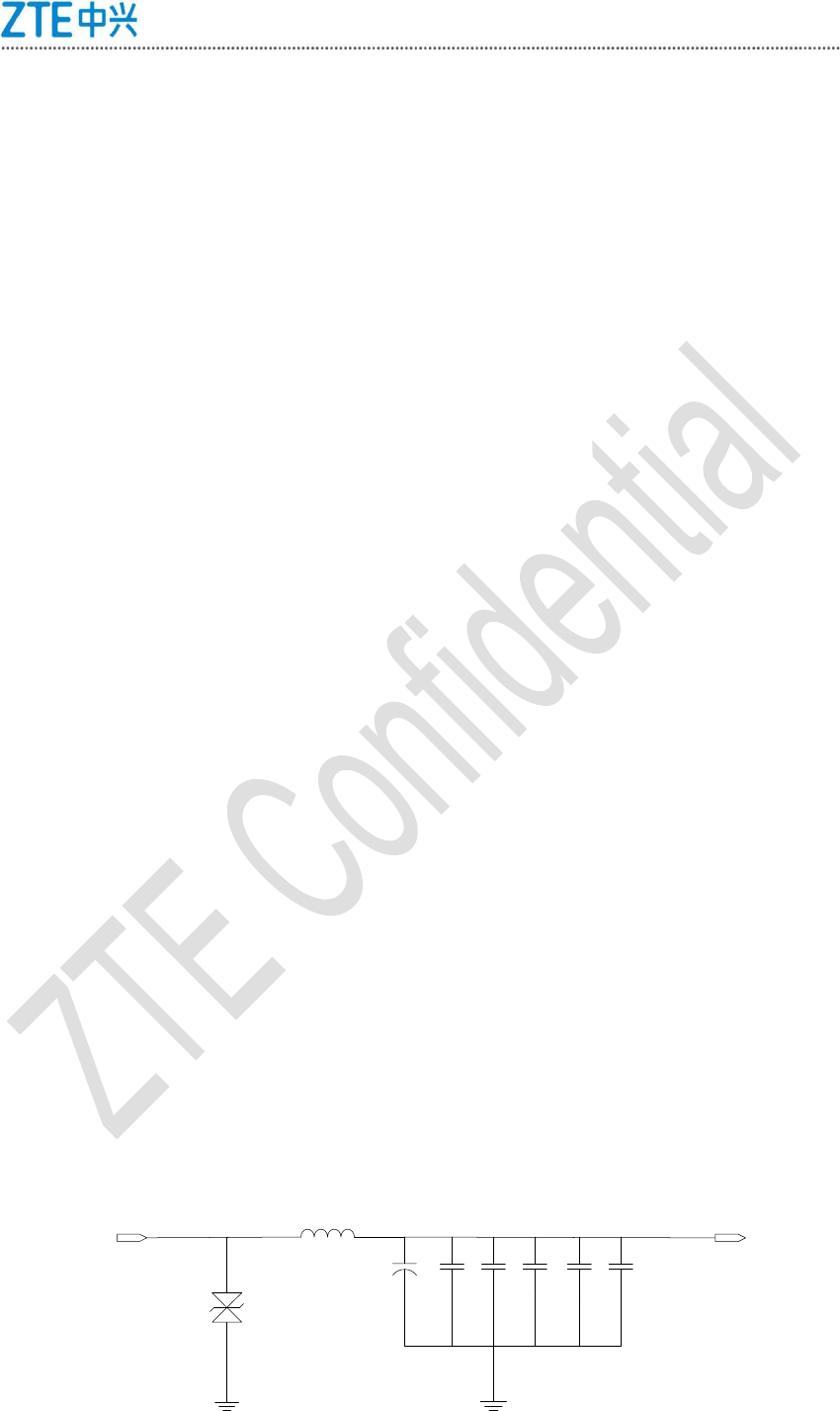
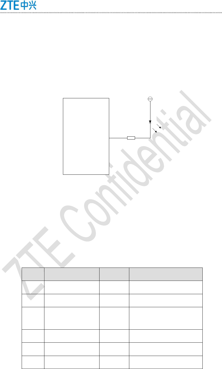
interfaces. Figure 3-2 illustrates the recommended power supply circuit.
VDD_3V6 VSYS
150uF
47uF
22uF
1uF
0.1uF
33pF
TVS
Bead
ZTE ZM8300G Module Hardware User Manual
<All rights reserved. No distribution without prior permission of ZTE.>
20
Figure 3-2 Recommended Power Supply Circuit
3.3.3 VIO Power
The ZM8300G module uses the VIO pin (PIN 37 on the LGA interface unit) to output 1.8
V power,whose output capacity is 20mA. The 1.8 V power can be used for level conversion or
pull-up. It is recommended that the 1.8 V power could not be used as a consumable power
supply. If the VIO pin is not used, leave it unconnected.
3.4 Control Signal Interfaces
3.4.1 Overview of Control Signals
The ZM8300G module provides the following LGA interface control signals:
startup/shutdown signal, hardware reset signal, wake-up signal, and status indication signal.
For details, see Table 3-3.
Table 3-3 Control Signals of the ZM8300G Module
Pin
Signal
I/O
Description
Remarks
32
POWN_ON
I
Startup/shutdown
signal
31
RESET_N
I
Hardware reset signal
6
WAKEUP_IN
I
Signal used by a host
to wake the module
Being
developed
7
WAKEUP_OUT
O
Signal used by the
module to wake a
host
8
PSM_MON
O
Module deep sleep
signal
5
STATE
O
Module status
indication signal
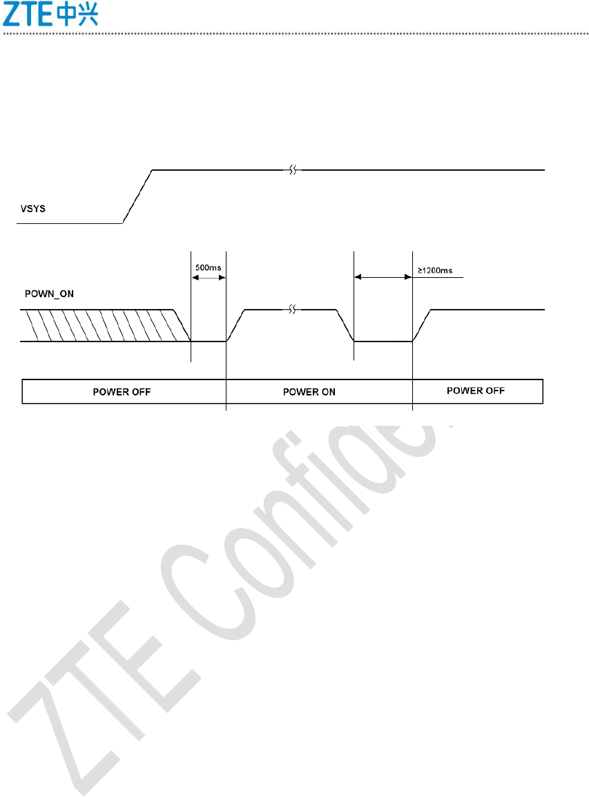
3.4.2 POWN_ON Signal
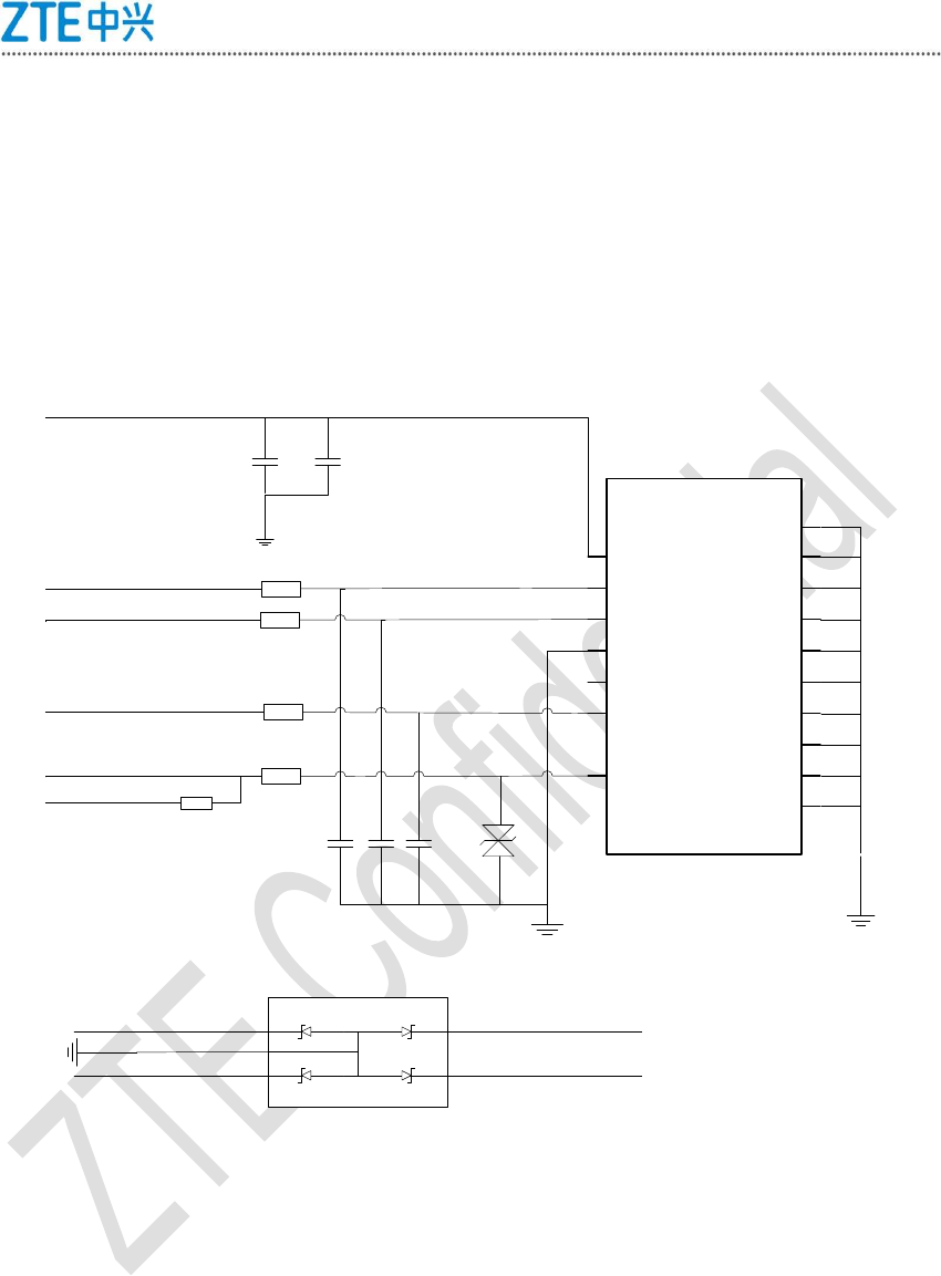
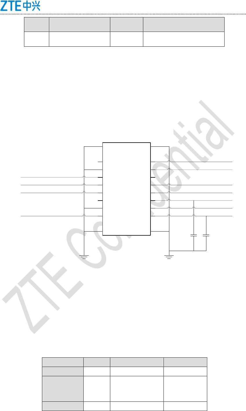
The POWN_ON pin is used for module power on/off function,low level trigger,1.8V pull-up
internal for module.after the power supply is normal for module,the module power on when
POWN_ON is drived low which must stay at least 500ms;after power on, if the POWN_ON
ZTE ZM8300G Module Hardware User Manual
<All rights reserved. No distribution without prior permission of ZTE.>
21
is drived low which stay at least 1200ms. The power off sequence is acomplished.note that
if the user want the module to power off after power supply is off,the POWN_ON should
be drived low for 1200ms and idle state should be at least 200ms. Power on/off sequence
timing diagram showed as FIG.3-3
Figure 3-3 Sequence timing of power on/off
For the design of the POWN_ON pin, the following schemes are available:
Scheme 1: If a customer wants to control the startup/shutdown of the module, connect the
POWN_ON signal pin to an AP and enable the AP to control the POWN_ON signal pin.
Scheme 2: If a customer wants to control the startup/shutdown of the module using a
button, design a button circuit on the system board. When using this scheme, pay attention
to ESD protection.
Scheme 3: If a customer requires that the module starts up immediately after being
powered on, ground the POWN_ON pin.
Figure 3-4 illustrates the three schemes.
ZTE ZM8300G Module Hardware User Manual
<All rights reserved. No distribution without prior permission of ZTE.>
22
AP ZM8300
b
c
e
POWN_ON
Ⅰ
Ⅲ
Ⅱ
S1
S2
0 Ω
2.2KΩ
1KΩ
Figure 3-4 Schemes for Controlling the Startup/Shutdown of the ZM8300G Module
Note that if scheme 3 is used, the module cannot enter the PSM sleep state. If a customer's
products prefer low power consumption, scheme 1 is recommended.
PIN 35 of the ZM8300G module can also provide the startup function. Specifically, after an
external logic high level is connected to the ZM8300G module, pull up PIN 35 to the
high-level state for 16 ms or more (1.25 V to 2.10 V, with the typical value being 1.5 V).
Then, the module starts up. Note that PIN 35 cannot provide the module shutdown function.
PIN 35 is a multiplexing pin. Therefore, to use PIN 35, communicate with ZTE FAE team in
advance.
3.4.3 RESET_N Signal
RESET_N is used for module hard reset function,low level trigger,1.8V pull-up internal for
module.after the module power on, RESET_N is drived low which must stay at least
500ms,note that the peroid for low level is no more than 8s or the module will power
off.Hard reset sequence timing diagram showed as FIG.3-5
ZTE ZM8300G Module Hardware User Manual
<All rights reserved. No distribution without prior permission of ZTE.>
23
Figure 3-5 Sequence timing of Hard reset
For the design of the RESET_N pin, two schemes are available, namely, being controlled
by an AP on the system board or being enabled by a button. Figure 3-6 illustrates the two
schemes.
AP ZM8300
b
c
e
RESET_N
Ⅰ
Ⅱ
S1
S2
2.2KΩ
1KΩ
Figure 3-6 Schemes for Controlling the Hardware Reset of the ZM8300G Module
3.4.4 WAKEUP_IN Signal
WAKEUP_IN is used to wake up module,default state is low level.when the pin is drived
from low to high,which wake up the module.note that when AP control module to wake
up,the high level should be at least 100ms.the anti-dithering for signal should be
considered, parallel capacitor is suggested to add near the pin.
ZTE ZM8300G Module Hardware User Manual
<All rights reserved. No distribution without prior permission of ZTE.>
24
Figure 3-7 illustrates the external drive circuit recommended for the WAKEUP_IN pin.
Alternatively, the 1.8 V IO of an external AP can be used to directly communicate with the
WAKEUP_IN pin.
ZM8300
WAKEUP_IN
2.2KΩ
b
c
e
VIO
AP
10 KΩ
Figure 3-7 Drive Circuit Recommended for the WAKEUP_IN Pin
Note that the WAKEUP_IN signal cannot wake theZM8300G module that is in the PSM
deep sleep state.
3.4.5 WAKEUP_OUT Signal
WAKEUP_OUT for ZM8300G module is used to wake up AP,default state is low level.when
the signal should be 100ms high level,which wake up AP.
3.4.6 PSM_MON Signal
PSM mode is UE Power Saving Mode. The fake power off state is applied in 3GPP REL12.
The module is on the register state but signalling can not be achieved. The attach or PDN
connection is not needed. The purpose is to save the power. Terminal calling is not needed
to answer immediately.when the terminal could get teminal calling service or date
transmission for actived state. The function should be supported for network.
For the waking up from PSM,ZM8300G could positively be waked up,besides the module
could be automatically waked up according to TAU TIME protocol. The module in PSM
state could be waked up for triggering the POWN_ON or PIN35 RESERVED no matter that
the timer of TAU is full or not.
The spcific trigger mode is same as power on sequence. The user could wake up the
module from external AP but should note that the RESERVED is multiplex pin. If the user
would like to use the function,please contact the ZTE FAE team in advance.
The PSM_MON is the indication signal for PSM mode.when the module is on the PSM
mode.the output of PSM_MON is low;when the module is on activeted mode,the output of
ZTE ZM8300G Module Hardware User Manual
<All rights reserved. No distribution without prior permission of ZTE.>
25
PSM_MON is high.
Note: Please connect PSM_MON to the MCU I/O that supports wakeup function.
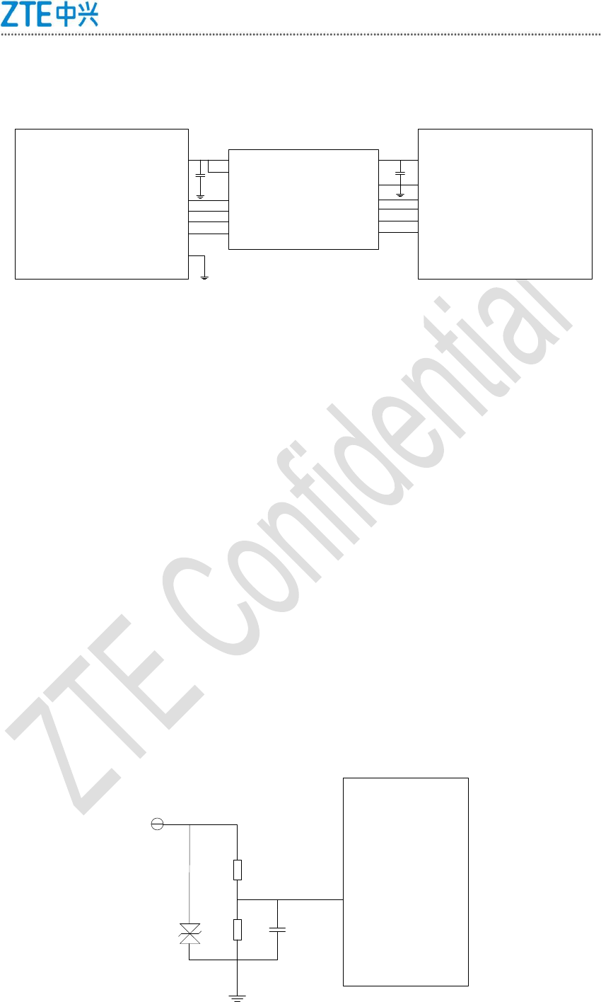
3.4.7 STATE Signal
The STATE is the indication for module operating state. The state could be designed to be
state indicator interface. The output pulse signalof the interface is used to control the single
color LED indicator. Defined LED state for ZM8300G showed in TABLE3-4
Table 3-4 Status Explanation for the LED Indicator
Indicator
Status
Meaning
solid light
conected to the network
flash
data transmission
solid off
sleep/PSM/not connected/power off
In actual applications, the STATE pin cannot directly drive the LED indicator and needs to
work with a transistor. Select a current limiting resistor for the LED indicator based on the
actual voltage drop and rated current of the LED indicator. When designing an LED
indicator, take ESD measures. Figure 3-8 illustrated the reference circuit.
STATE
ZM8300
STATE 2.2KΩ
b
c
e
VSYS
Figure 3-8 STATE Status Indicator Circuit
3.5 DEBUG_UART Interface
The ZM8300G module provides a two-wire DEBUG_UART serial port for module
debugging. Tests points or JTAG&UART debugging connectors (see section 3.12.2) should
be designed for the two signals. Table 3-5 provides information about pins of the debug
ZTE ZM8300G Module Hardware User Manual
<All rights reserved. No distribution without prior permission of ZTE.>
26
interface. Note that the serial port is used only for module debugging and must not be used
for AT command interaction.
Table 3-5 Description of the DEBUG_UART Interface
Pin
Signal
I/O
Description
Remarks
15
DEBUG_UART_RX
I
To receive data
1.8 V power domain
16
DEBUG_UART_TX
O
To transmit data
1.8 V power domain
3.6 BLSP Interfaces
3.6.1 Pin Description
The design of ZM8300G interface include two groups 4-line BLSP(BAM(Bus access
manager)Low-speed Peripheral)interface.the interface is configured through UART、SPI、
I2C and GPIO by software.the default configuration of 2-line AT UART serial interface is
BLSPB_0/1. Desciption of interface configuration for BLSP showed table3-6.
Table 3-6 Configuration of BLSP Resources
Con
figu
rati
on
BLSPA
BLSPA_0 (PIN17)
BLSPA_1 (PIN18)
BLSPA_2 (PIN19)
BLSPA_3 (PIN20)
BLSPB
BLSPB_0 (PIN21)
BLSPB_1 (PIN22)
BLSPB_2 (PIN23)
BLSPB_3 (PIN24)
1
4-pin UART
UART_TX
DO
UART_RX
DI
UART_CTS
DI
UART_RTS
DO
2
2-pin UART
+ 2-pin I2C
UART_TX
DO
UART_RX
DI
I2C _SDA
B
I2C _SCL
B
3
4-pin SPI
SPI_MOSI
B
SPI_MISO
B
SPI_CS_N
B
SPI_CLK
B
4
2-pin GPIO
+ 2-pin I2C
GPIO_XX
B
GPIO_XX
B
I2C_SDA
B
I2C _SCL
B
5
4 GPIOS
GPIO_XX
B
GPIO_XX
B
GPIO_XX
B
GPIO_XX
B
6
2-pin UART
+2-pin GPIO
UART_TX
DO
UART_RX
DI
GPIO_XX
B
GPIO_XX
B
3.6.2 UART Interfaces
The BLSP pins of the ZM8300G module can be configured as two-pin and four-pin serial bus
UART interfaces. The ZM8300G module can perform serial data transmission and AT
communication with external devices using the UART interfaces. In addition to traditional
UART characteristics, the UART interfaces provided by the ZM8300G module have the
ZTE ZM8300G Module Hardware User Manual
<All rights reserved. No distribution without prior permission of ZTE.>
27
following characteristics:
1) The UART_DM interface supports high-speed UART running, with the maximum rate
reaching 4 Mbit/s.
2) Strengths of the UART_DM block: The RX and TX rate control data movers have
separate CRCI channels. An SRAM can achieve a large RX and TX FIFOX and obtain a fast
system bus (AHB interface). When the data movers are unavailable, the traditional interrupt is
directly saved to the microprocessor.
3) The TX and RX channels of a UART_DM interface primarily differ from those of a basic
UART interface in the following aspects:
a) FIFO is implemented in the SRAM.
b) FIFO control and IRQ generation are implemented in the DM control block.
4) The UART interfaces can be used as diagnostic interfaces.
Note that the UART level of ZM8300G is 1.8V. If external AP interface is 3.3V, the level
shifting circuit is applied(level shifting IC:TXB0104RUTR) when ZM8300G carry out AT
communication. The reference design circuit for UART is showed as FIG3-9
ZM8300 Level
Shift AP
VIO VCCA
OE VCCB
GND
VCC_3V3
UART
(1.8v)
A1~A4
GND GND
B1~B4
UART
(3.3v)
Figure 3-9 UART Reference Circuit
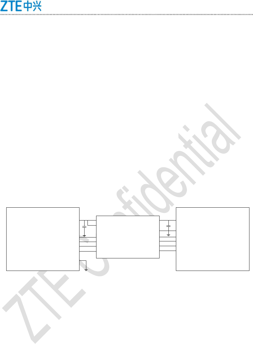
3.6.3 SPI Bus Interface
The SPI is a four-wire (MISO, MOSI, CS, and CLK) synchronous serial data link. The SPI bus
interface has the following characteristics:
1) When the SPI bus interface works as the master device, the clock frequency of BLSPA
can reach 50 MHz and that of BLSPB can reach 38 MHz.
2) When the SPI bus interface initiates data transmission as the master device, multiple
slave devices can be supported by means of the chip select (CS) signal.
3) Explicit communication framing, error checking, and defined data word lengths are
absent. Therefore, data transmission must strictly observe the raw bit level.
4) When working as the SPI master device, the SPI bus interface supports the following
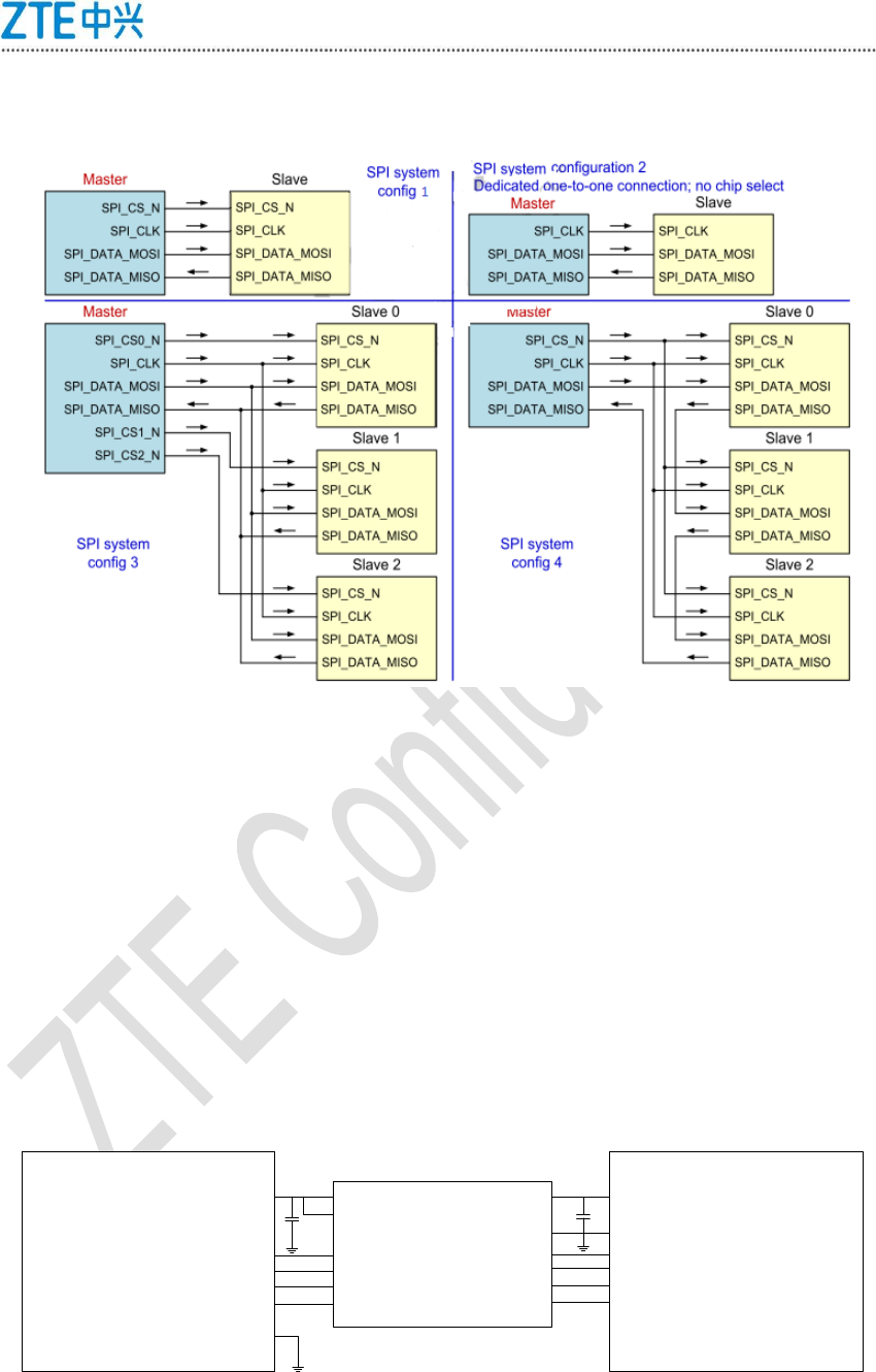
ZTE ZM8300G Module Hardware User Manual
<All rights reserved. No distribution without prior permission of ZTE.>
28
system configurations (restricted by the SPI protocol). Figure 3-10 illustrates the system
configurations.
Figure 3-10 SPI System Configurations
Pay attention to the following points during design:
1) If the SPI bus reaches the highest frequency during running, its priority must be higher
than the priorities of other BLSP bus interfaces.
2) If one group of SPI buses is shared by multiple devices, ensure that these devices are
close to each other, with the goal of avoiding signal integrity problems caused by long bus
branches.
3) The SPI interface provided by the ZM8300G module is a 1.8 V IO interface. If the
ZM8300G module needs to work with a peripheral that uses a different level, add a level
conversion circuit. Figure 3-11 illustrates the recommended level conversion circuit. The level
conversion chip (TI: TXB0104RUTR) is recommended.
ZM8300 Level
Shift Peripheral
Chip
VIO VCCA
OE VCCB
GND
VCC_3V3
SPI
(1.8v)
A1~A4
GND GND
B1~B4
SPI
(3.3v)
Figure 3-11 SPI Level Conversion Circuit

ZTE ZM8300G Module Hardware User Manual
<All rights reserved. No distribution without prior permission of ZTE.>
29
3.6.4 I2C Bus
I2C is a two-wire bus used for communication between ICs and supports all IC processes
(NMOS, CMOS, and bipolar). The two signal lines, namely, the serial data (SDA) line and the
serial clock (SCL) line, transfer information between connected devices. Each device (a
microcontroller, memory, LCD driver, audio DAC, or keyboard interface) is identified by a
unique address and used as a transmitter or a receiver, depending on the provided functions.
The I2C interface has the following characteristics:
1) The two-wire bus is used for communication between chips.
2) Supports all ICs on the I2C bus. Each device has a unique address and can be used as a
transmitter or a receiver.
3) Supports external functions, including cameras, microcontrollers, FM radio chips, LCD
drivers, audio DACs, and keyboard interfaces.
4) An I2C controller provides an interface between advanced high-performance buses
(AHBs) and an industry-standard I2C serial bus to handle the I2C protocol and release chip
processors and interfaces, so that the chip processors and interfaces can handle other
services.
5) The I2C interface works in standard mode (100 kbit/s) or high-speed mode (400 kbit/s).
The operating frequency of the ZM8300G I2C interface reaches 400 kHz. When the ZM8300G
I2C interface works only in master mode, the operating frequency may reach 1 MHz.
6) When using the I2C bus, configure the corresponding BLSP pin as an open drain output
GPIO. In this case, an external device needs to use VIO to provide pull-up. The group of I2C
buses provided by the ZM8300G module (BLSPA_2 and BLSPA_3) already has pull-up. To
configure other I2C buses, a customer needs to add an external pull-up. Figure 3-12 illustrates
an I2C reference circuit.
ZTE ZM8300G Module Hardware User Manual
<All rights reserved. No distribution without prior permission of ZTE.>
30
ZM8300
I2C_SCL
I2C_SDA
IC 1
IC n
…
…
CLK
DATA
VIO
CLK
DATA
Figure 3-12 I2C Reference Circuit
3.7 GPIO Interfaces
In addition to BLSP pins, which can be configured as general-purpose input/output (GPIO)
interfaces, reserved pins and some dedicated pins of the ZM8300G module can also be
multiplexed as GPIO interfaces. For details, see Table 3-7. Customers can use these IO
interfaces for control functions. By default, all IO interfaces of the ZM8300G module are PD.
The multiplexing functions of the reserved pins are being developed.
Table 3-7 ZM8300G GPIO Resources
Multiplexed as GPIO Interfaces
Pin
Signal
I/O
Description
Remarks
34
RESERVED
B
GPIO
VIO (1.8 V) power
domain
35
RESERVED
26 to 29
PCM audio interface
5 to 8
Control signal
interface
ZTE ZM8300G Module Hardware User Manual
<All rights reserved. No distribution without prior permission of ZTE.>
31
3.8 USIM Interface
3.8.1 Pin Description
The baseband processor of the ZM8300G module integrates 2.85 V and 1.8 V USIM
interfaces that support automatic detection and meet requirements specified by the ETSI
and requirements specified for IMT-200 SIM cards. Figure 3-8 describes the USIM interface
signals.
Table 3-8 Description of USIM Signals
Pin
Signal
I/O
Description
Remarks
58
USIM_CLK
O
USIM clock signal
57
USIM_DATA
B
USIM data signal
The 10K resistor inside
the module is pulled up
to the USIM_PWR.
56
USIM_RESET
O
USIM reset signal
46
USIM_PWR
PO
USIM power
The module adapts to
1.8 V/2.85 V USIM
cards.
55
USIM_DET
I
Detection of the USIM
card hot plugging
function
If the hot plugging
function is unavailable,
leave this pin not
connected.
3.8.2 Electrical Characteristics and Design Points
Instead of reserving a slot for a USIM card, the ZM8300G module connect USIM
signals using an LGA pad. During design, note that ESD circuit protection is added for all
USIM signals (do not add ESD protection circuit if eSIM is designed), and ensure that the
protection device is close to the card slot. To meet requirements of the 3GPP TS 51.010-1
protocol and EMC certification, locate the USIM card slot near the USIM signal interface of
the ZM8300G module, to prevent signal integrity from being affected due to severely
distorted waveforms that result from a long distance between the USIM card slot and the
USIM signal interface. In addition, ground the USIM_CLK and USIM_DATA signal lines.
Connect a 0.1 uF capacitor and a 33 pF capacitor in parallel between USIM_PWR and
GND, and connect capacitors in parallel between USIM_CLK/USIM_RESET/USIM_DATA
ZTE ZM8300G Module Hardware User Manual
<All rights reserved. No distribution without prior permission of ZTE.>
32
and GND, with the goal of filtering out interference from RF signals. Then, connect a
zero-ohm resistor in series to the USIM_DATA, USIM_CLK, and USIM_RESET signal lines
as a measure reserved for ESD protection and EMI design.If the hot plug for SIM is applied,
contact ZTE FAE team.
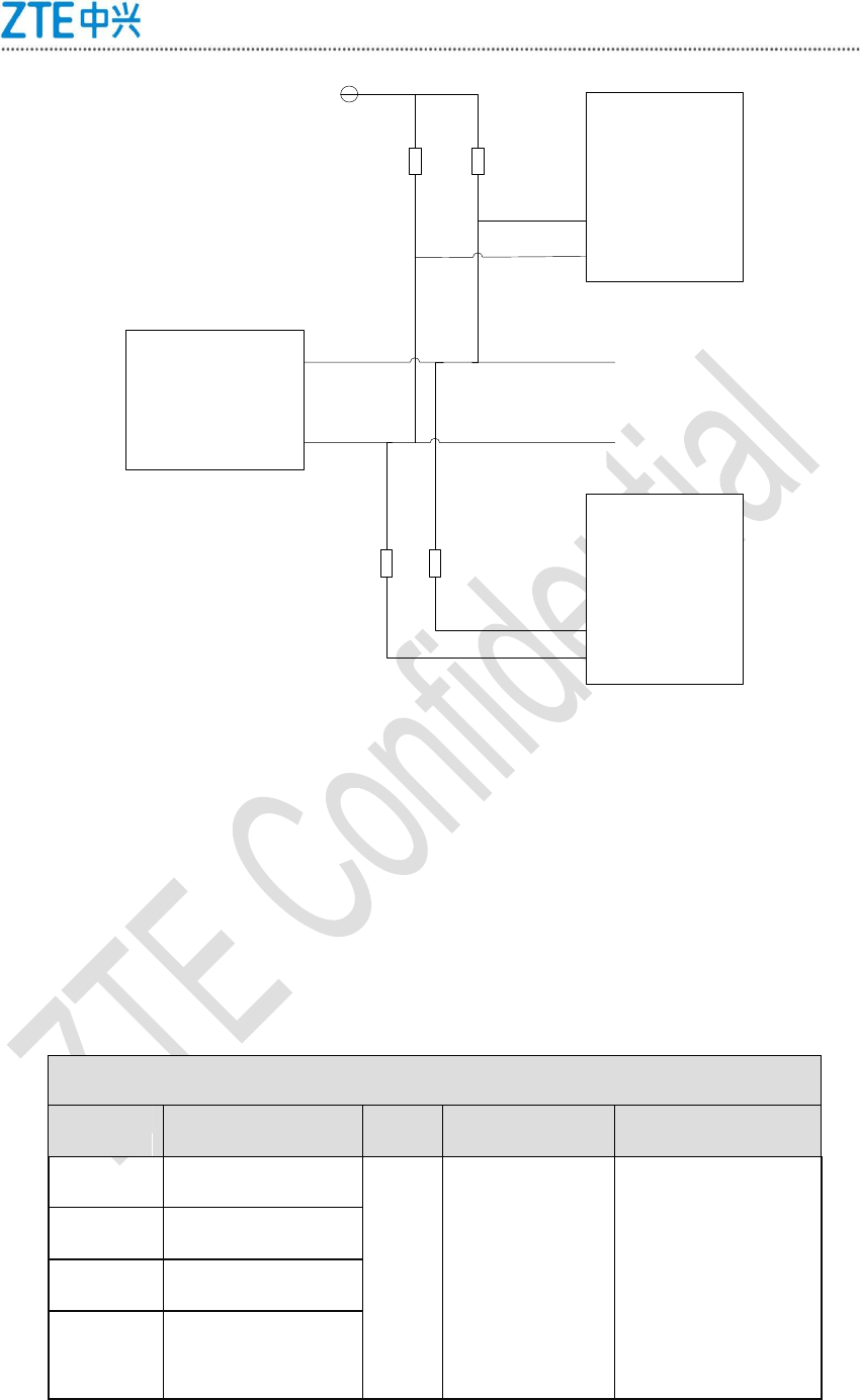
3.8.3 Circuit Recommended for the USIM Card Interface
Figure 3-13 illustrates the peripheral circuit recommended for the USIM card interface.
USIM
Slot
sw c7 c6 c5 c3 c2 c1
GND[0~9]
USIM_PWR
USIM_RESET
USIM_CLK
USIM_DATA
USIM_DET
VIO
33pF
0.1uF
0Ω
0Ω
0Ω
1KΩ
NA
NA
NA
NA
1
2
34
5
USIM1_DATA
USIM_PWR
USIM1_RESET
USIM1_CLK
Overvoltage
Protectors
USIM1_RESET
USIM1_CLK
USIM1_DATA
Figure 3-13Peripheral Circuit Recommended for the USIM Card Interface
In addition to the method of designing a USIM card slot on the system board, customers can
design an eSIM chip. The ST or Gemalto scheme is recommended.
3.9 USB Interface
3.9.1 Pin Description
The ZM8300G module provides an integrated USB transceiver, which complies with
USB2.0 and supports the high speed mode (480 Mbit/s), full speed mode (12 Mbit/s), and
low speed mode (1.5 Mbit/s). The USB interface primarily applies to AT commands, data
ZTE ZM8300G Module Hardware User Manual
<All rights reserved. No distribution without prior permission of ZTE.>
33
transmission, software commissioning, and software upgrade. Table 3-9 describes USB
signals.
Table 3-9 Description of USB Signals
Pin
Signal
I/O
Description
Remarks
40
USB_VBUS
I
USB PHY power detection
Only used for USB PHY
detection and not used
as a power supply
52
USB_DP
AI/O
USB differential data bus
(positive)
90 ohm differential
impedance
53
USB_DM
AI/O
USB differential data bus
(negative)
90 ohm differential
impedance
39
USB_ID
I
USB_ID detection signal
OTG function; No
connection when
working as a device.
51
GND
GND
3.9.2 Design Points and Recommended Circuit
For detailed information about USB 2.0 specifications, access http://www.usb.org/home.
Figure 3-12 illustrates a circuit recommended for the USB interface. To ensure that
subsequent commissioning and upgrading operations can be smoothly performed, customers
need to design a USB 2.0 connector on an external system board. ZTE recommends the
following model: MOLEX: 1051330001 and LS: GU073-5P-SE-E2000. The bead in Figure
3-14 can be replaced with a resistor. If no high-speed data services are involved and the USB
differential signals are properly protected, the common mode inductor can be removed.
ZM8300
USB
Connector
1 2 3 4 5
S1 S2 S3 S4
VBUS
DM
DP
ID
GND
USB_VBUS
USB_DM
USB_DP
USB_ID
Bead
1000pF
47K
NA
Common Mode
Noise Filter

ZTE ZM8300G Module Hardware User Manual
<All rights reserved. No distribution without prior permission of ZTE.>
34
Figure 3-14 Circuit Recommended for the USB Interface
To ensure that the designed USB interface complies with USB 2.0 specifications, observe
the following guidelines:
1) Ensure that USB differential signal lines have a complete reference ground and the
impedance of PCB differential signal lines is 90 ohms.
2) Note the impact of the junction capacitor of the ESD protection device on the
high-speed USB data line. Generally, select a junction capacitor with the capacitance less
than 2 pf, and locate the ESD protection device near the USB interface.
3) Ensure that USB differential signal lines are far away from crystal lines, oscillator lines,
and RF signal lines and have a complete reference ground plane both above and below. In
addition, ensure that USB differential signal lines in the same layer are protected by ground
cables.
3.10 Audio Interfaces
3.10.1 Pin Description
The ZM8300G module provides PCM and I2S digital audio interfaces, which share the same
physical interface. That is, the ZM8300G module supports only the PCM interface or the I2S
interface at a time. The audio interface can be connected to a voice CODEC chip, for example,
WCD9330 from Qualcomm. Table 3-10 describe the two types of audio interfaces.
Table 3-10 Description of Digital Audio Interfaces
Pin
PCM
Description
I2S
Description
26
PCM_DIN
PCM audio data RX signal
I2S_D0
I2S audio data D0 signal
27
PCM_DOUT
PCM audio data TX signal
I2S_D1
I2S audio data D1 signal
28
PCM_CLK
PCM audio clock signal
I2S_SCLK
I2S audio clock signal
29
PCM_SYNC
PCM audio synchronization
signal
I2S_WS
I2S audio chip select
signal
3.10.2 Design Points
Both the PCM and I2S interfaces use digital, square wave signals. After adding a level
conversion circuit, pay attention to signal integrity. To ensure signal integrity, connect a
resistor in series and a capacitor in parallel to signal lines as impedance matching and
filtering means. When designing a PCB, note the continuity of the signal line impedance.
Figure 3-15 illustrates the recommended voice circuit. If the CODEC voice signal interface
ZTE ZM8300G Module Hardware User Manual
<All rights reserved. No distribution without prior permission of ZTE.>
35
uses the 3.3 V level, level conversion is required (TI: TXB0104RUTR). If a customer requires
I2S voice, PIN 34 of the ZM8300G module can provide the I2S_MCLK signal. Note that PIN 34
is a multiplexing pin. Therefore, to use PIN 34, communicate with ZTE FAE team in advance.
ZM8300 Level
Shift Codec
IC
VIO VCCA
OE VCCB
GND
VCC_3V3
PCM/I2S
(1.8v)
A1~A4
GND GND
B1~B4
PCM/I2S
(3.3v)
Figure 3-15 Recommended Audio Circuit
3.11 ADC/MPP Interfaces
3.11.1 Pin Description
The ZM8300G module provides two ADC/MPP interfaces (PIN 42 and PIN 44), which can be
multiplexed as analog multiplexer inputs and current sinks.
1) When working as an ADC analog input interface, the analog multiplexer inputs interface
samples external voltages and temperatures. The input voltage should be within the range of
0 V to 1.8 V.
2) When working as an input current source, the current sinks interface drives an LED
indicator and controls its brightness at 5 mA intervals, with the input current within the range
of 5 mA to 40 mA. When the MPP pin is used to light an indicator, the power consumption of
the ZM8300G module increases.
3.11.2 Design Points
The following figures illustrate the two functions multiplexed on the MPP interface.
ZM8300
MPP
(ADC)
1000pF
Battery
ZTE ZM8300G Module Hardware User Manual
<All rights reserved. No distribution without prior permission of ZTE.>
36
Figure 3-16 ADC Interface Circuit
When the two pins are used to sample ADC analogs (for example, to sample the battery
voltage), ensure that the input voltage is within the allowed range. It is recommended that a
bleeder circuit be designed and a bleeder resistor of hundreds of kilo-ohms be used, with the
goal of reducing the leakage current. In addition, provide the designed circuit with ESD
protection. To improve the sampling accuracy, ensure a good reference ground for the ADC
PCB circuit.
ZM8300
VSYS
MPP
( crrent sink )
Figure 3-17 MPP Indicator Lighting
Provide ESD protection when using the interface to drive an LED indicator.
3.12 JTAG Interface
3.12.1 Pin Description
The joint test action group (JTAG) interface of the ZM8300G module complies with
ANSI/IEEE Std.1149.1-1990. Table 3-11 describes JTAG signals.
Table 3-11 Description of the JTAG Signals
Pin
Signal
I/O
Description
T1
JTAG_PS_HOLD
-
Power setup holding signal
T2
JTAG_TDI
DI-PU
JTAG debug data input signal
T3
JTAG_TMS
DI-PU
JTAG debug mode selection
signal
T4
JTAG_TDO
Z
JTAG debug data output signal
T5
JTAG_TCK
DI-PU
JTAG debug clock signal
T6
JTAG_RESOUT_N
DO
JTAG reset output signal
ZTE ZM8300G Module Hardware User Manual
<All rights reserved. No distribution without prior permission of ZTE.>
37
Pin
Signal
I/O
Description
T7
JTAG_TRST_N
DI-PD
JTAG debug reset signal
3.12.2 Design Points
The ZM8300G module provides a test point pad for the JTAG interface. it is recommended
that customers design a connector (recommended material: PANASONIC: AXE216044D),
with the goal of resolving difficult problems. Figure 3-18 illustrates the recommended
connector circuit, which includes JTAG and DEBUG_URAT debug interfaces. If failing to
design a connector due to limited dimensions, design JTAG and DEBUG_URAT test points on
the system board.
S1 S4
S2 S3
1 3 5 7 9 11 13 15
2 4 6 8 10 12 14 16
JTAG_TRST_N
JTAG_TMS
JTAG_TDI
DEBUG_UART_TX
JTAG_PS_HOLD
JTAG_RESOUT_N
JTAG_TCK
JTAG_TDO
VIO
DEBUG_UART_RX
VSYS
0.1uF
0.1uF
Figure 3-18 Circuit for a JTAG/UART Debug Connector
3.13 Antenna Interfaces
3.13.1 Pin Description
The ZM8300G module provides two antenna pads. Table 3-12 describes the two antenna
pads (including the ground points next to the pads).
Table 3-12 Antenna Interfaces
Signal
Pin
Description
Remarks
GND
1
Grounding
MAIN_ANT
2
RF main antenna
interface
50 Ω
GND
3
Grounding
ZTE ZM8300G Module Hardware User Manual
<All rights reserved. No distribution without prior permission of ZTE.>
38
Signal
Pin
Description
Remarks
GND
10
Grounding
GPS_ANT
11
GPS antenna
interface
50 Ω
GND
12
Grounding
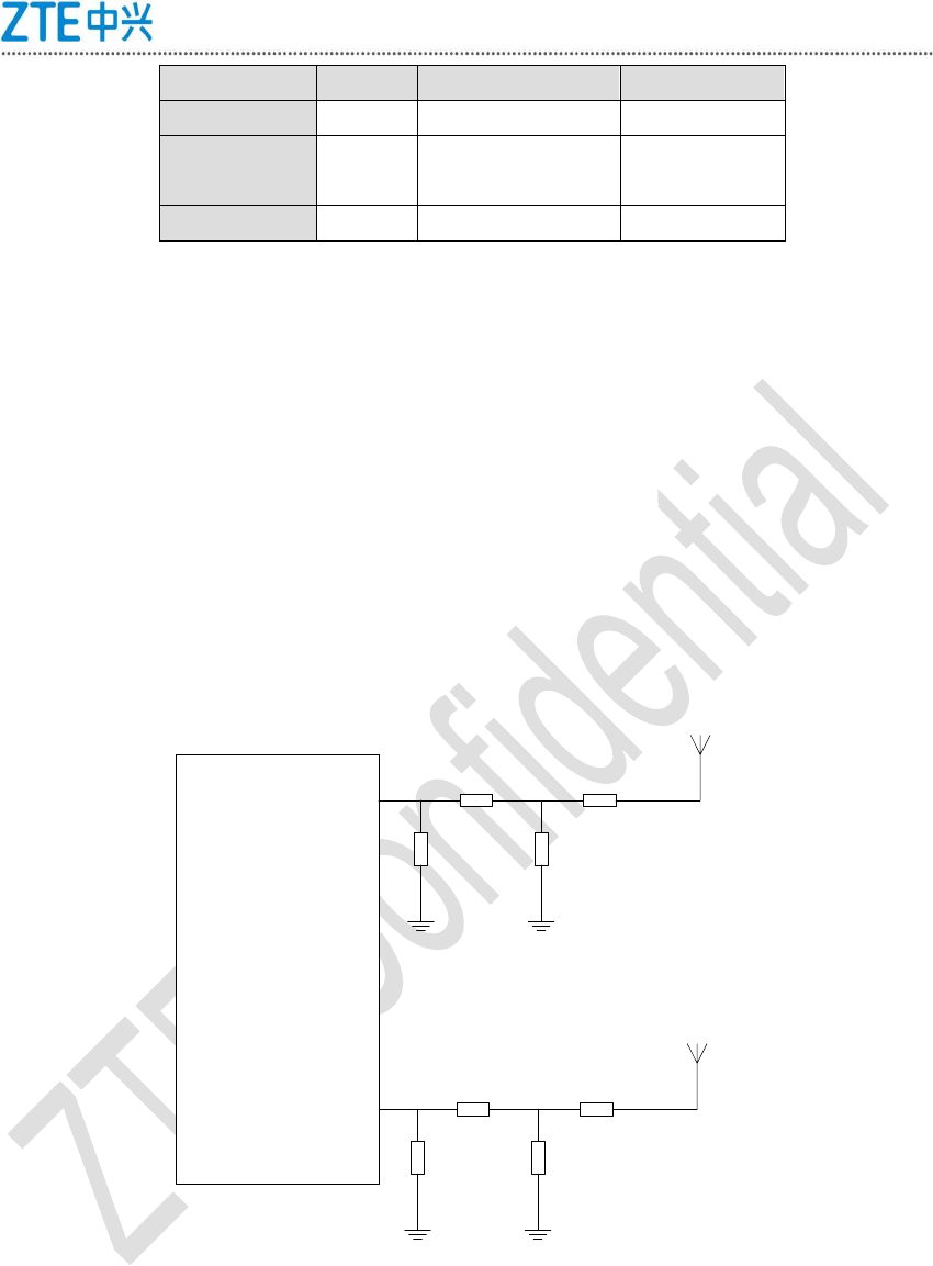
3.13.2 Antenna Design Points
Antennas are easily affected by external environments, for example, antenna locations,
antenna occupied room, and surrounding devices. The ZM8300G module provides two
antenna pads for antenna design, with a ground point available to each side of each pad, to
ensure good grounding. Figure 3-17 illustrates a reference circuit for antenna design. The
dual-L matching network helps improve the RF performance. During the design, place the
component near the module, and place the antennas near the matching network, so as to
reduce path loss. Figure 3-19 illustrates the recommended antenna circuit, which includes
resistors, capacitors, and inductors.
ZM8300
ANT
ANT
MAIN_ANT
GPS_ANT
Figure 3-19 Reference Circuit for the Antenna Interfaces
For detailed requirements for antenna design, see section 4.6.
ZTE ZM8300G Module Hardware User Manual
<All rights reserved. No distribution without prior permission of ZTE.>
39
4 RF Characteristics
4.1 About This Chapter
4.1.1 Power Supply
The voltage input to the ZM8300G module should be within the range of DC 3.0 V to 4.2 V,
with the typical value being 3.6 V. For details, see Table 4-1.
Table 4-1 Required Input Voltage Range
Parameter
Minimum
Value (V)
Typical
Value (V)
Maximum
Value (V)
Input voltage
3.0
3.6
4.2
4.1.2 Operating Current
Table 4-2 provides part of operating current data of the ZM8300G module.
Table 4-2 Operating Current
Mode
Status
Average
Current
Remarks
CAT M
Sleep current
0.7 mA
IDLE
1.07mA
2.56Sdrx Online
Average operating
current (UL)
115 mA
LTE 10MHz bandwidth embedded data call@0dBm
TX,UL only,375 kbps;
Average operating
current (DL)
112 mA
LTE 10MHz bandwidth embedded data call@0dBm
TX,DL only,375 kbps;
CAT NB
Sleep current
0.7 mA
IDLE
1.47mA
2.56Sdrx Online
Average operating
current (UL)
50 mA
LTE 10MHz bandwidth embedded data call@0dBm
TX,UL only,62.5 kbps(15KHz single tone);
Average operating
current (DL)
50 mA
LTE 10MHz bandwidth embedded data call@0dBm
TX,UL only,21kbps(multi tone);
◆Note: The lab data provided by Qualcomm is used.
4.2 Reference Design for RF Layout
For the RF part of a PCB, ensure that the characteristic impedance of the RF line is 50 ohms.
The impedance of an RF line is generally determined by the line width (W), dielectric constant
of the material, distance away from the reference signal layer (H), and gap between the RF
ZTE ZM8300G Module Hardware User Manual
<All rights reserved. No distribution without prior permission of ZTE.>
40
line and the ground (S). The microstrip and stripline are generally used to control the
characteristic impedance of an RF line.
Microstrip Line Design on a 2-Layer PCB
To ensure RF performance and reliability, refer to the following rules specified for PCB layout:
Use an impedance simulation tool to ensure that the characteristic impedance of an RF
line is 50 ohms.
Connect the entire ground pin that is adjacent to an RF pin to the main ground. Do not
connect it to a thermal pad.
Minimize the distance between an RF pin and an RF connector.
Ensure an adequate forbidden area for the pad or solder joint of an antenna connector.
Ensure a complete reference ground plane for an RF line. In addition, add a row of
ground holes between the RF line and the surrounding area to effectively improve RF
performance. Ensure that the distance between the ground and the RF line is equal to or
greater than twice the line width (2 x W).
4.3 Test Standard for Conducted RF
The ZM8300G module meets RF requirements specified in 3GPP TS 36.521-1.
4.4 Requirements for Antenna Design
4.4.1 Key Points for Antenna Design
Antennas are very important for wireless communication products, because antenna
performance directly affects the communication quality of the products. Before designing
antennas, select antenna types based on available space and application scenarios. Table
4-6 provides detailed information about how to select NB-IOT antennas.
Table 4-6 Detailed Information About How to Select NB-IOT Antennas
Product Type
Characteristics of Application
Scenarios
Antenna Type Selection
ZTE ZM8300G Module Hardware User Manual
<All rights reserved. No distribution without prior permission of ZTE.>
41
Smart meter reading products such
as water meters, electricity meters,
and gas meters
Meters are installed at remote
locations, surrounding
environments are complex, the
signal attenuation is large, and
the signal quality is poor.
1. Internal antenna
2. High-gain antenna
3. Omni-directional
antenna
4. Low cost
Car detector
Car detectors are buried in the
ground, and the signal quality is
poor.
Smart city products such as smart
streetlights and smart garbage
cans
Smart city products are installed
outdoors, so they must be easy to
install and require good
waterproofing measures.
1. External antenna
2. Waterproof and
corrosion resistant
3. Low cost
Mobile products
Mobile products provide the
positioning function. When
mobile products move, signals
change and are unstable.
1. GPS antenna with
excellent performance
2. Omni-directional
antenna pattern, if
possible
3. Low cost
Tracker products
Tracker products are carried by
people or animals, feature small
sizes, and have high
requirements for the positioning
function.
1. GPS antenna with
excellent performance
2. Considering the
impact of people or
animals on the antenna
efficiency
3. Small sizes
4. Low cost
Passive parameters used to measure the performance of an antenna include the antenna
efficiency, VSWR, return loss (S11), polarization, and radiation pattern, which are described
as follows.
4.4.2 Antenna Efficiency
The efficiency of an antenna refers to the ratio of the power radiated by the antenna to the
effective input power. The power radiated by an antenna is generally less than the input
power due to antenna loss and cable loss. The antenna loss is primarily reflected by the
antenna efficiency. Specifically, high antenna efficiency indicates low antenna loss. The
antenna efficiency is affected by the VSWR/S11 and antenna clearance area. An antenna

ZTE ZM8300G Module Hardware User Manual
<All rights reserved. No distribution without prior permission of ZTE.>
42
clearance area is an area without metal. A large clearance area indicates high antenna
efficiency. If an RF output port is connected to the input port of an antenna using a cable, the
loss caused by the cable needs to be considered. Generally, the loss caused by a cable is
proportional to the cable length and frequency. Therefore, use short cables if possible. To
enable a ZM8300G module to obtain better RF radiation performance, it is recommended that
the antenna efficiency be greater than 45% (within all frequency bands).
4.4.3 VSWR
When a feeder does not match an antenna, an incident wave and a reflected wave co-exist in
the feeder. For the in-phase position of the two waves, the amplitude has maximum value,
and an antinode is formed. For the reverse-phase position of the two waves, the amplitude
has minimum value, and a wave node is formed. The amplitudes at other points are between
the antinode and the wave node. Such a combined wave is called a standing wave. The ratio
of the voltage at an antinode of a standing wave to the voltage at a node of the standing wave
is called the voltage standing wave ratio (VSWR). A small VSWR indicates better antenna
performance. The VSWR of an antenna can be measured using a vector network analyzer.
For the ZM8300G module, it is recommended that the VSWR be less than 3.0.
4.4.4 S11
The S11 indicates the transmit efficiency of an antenna. A large S11 indicates more returned
power and poor antenna efficiency. The S11 can be measured using a vector network
analyzer. For the ZM8300G module, it is recommended that the S11 be less than -8 dB.
4.4.5 Polarization
The antenna polarization is a parameter used to describe the spatial orientation of the
antenna-radiated electromagnetic field vector. As the electric field has a constant relationship
with the magnetic field, the spatial orientation of the electric field vector is generally used as
the polarization direction of antenna-radiated electromagnetic waves. Generally, linear
polarization, circular polarization, and elliptical polarization are available. For the ZM8300G
module, linear polarization is recommended for its antennas.
4.4.6 Radiation Pattern
The radiation pattern describes the distribution of antenna radiation in space, especially the
distribution in the far field region, and indicates the characteristics of a field, for example, the
product of the size/field strength and the distance, radiant intensity, directivity, absolute gain,
and relative gain of a specified component of the electromagnetic field.
Since the incident wave of a base station is horizontal, a wireless terminal has optimal
reception performance when the radiation pattern of its receive antenna is omni-directional in
the horizontal plane. For the ZM8300G module, omni-directional radiation pattern is
recommended for its antennas.
ZTE ZM8300G Module Hardware User Manual
<All rights reserved. No distribution without prior permission of ZTE.>
43
4.4.7 Requirements for IoT Antenna Design
Table 4-7 lists requirements for basic parameters for designing an IoT antenna.
Table 4-7 Requirements for Antenna Design
Parameter
Requirement
VSWR
<2
Gain (dBi)
>1
Maximum input power
(dBm)
25.7
Input impedance (ohm)
50
Polarization
Linear polarization
4.4.8 Precautions for Early Antenna Design
When determining a location for an antenna, observe the following guidelines: Ensure that the
location and the base station served by the antenna are in the horizontal direction, with the
goal of enabling the antenna to produce the highest efficiency; ensure that the location is far
away from components or chips that may generate electromagnetic interference such as a
switch-mode power supply, data line, and chip; ensure that the location is unreachable by
hand, with the goal of preventing hands from causing antenna attenuation. In addition,
consider radiation reduction and structure feasibility. Therefore, at the beginning of antenna
design, invite structure engineers, ID engineers, circuit engineers, and antenna engineers to
assess the layout. If a system board needs to process signals from multiple antennas,
consider co-channel interference.
ZTE has certified multiple antenna vendors. If required, ZTE can recommend several antenna
vendors for antenna design.

ZTE ZM8300G Module Hardware User Manual
<All rights reserved. No distribution without prior permission of ZTE.>
44
5 Mechanical Characteristics
5.1 About This Chapter
This chapter describes the mechanical structure of the ZM8300G module, covering the
following aspects:
Assembly procedure
Repair procedure
EMC and ESD protection
5.2 Assembly Procedure
5.2.1 Overview
The ZM8300G module is mounted on a five-layer antistatic tray with anti-shock foam,
vacuumized, and placed in a carton, with the goal of preventing the module from collision or
oxidization.
5.2.2 Steel Mesh
It is recommended that a 0.1 mm thick steel mesh be designed for the ZM8300G module.
For the design of a steel mesh, refer to Figure 5-1 and Figure 5-2 (in mm).
ZTE ZM8300G Module Hardware User Manual
<All rights reserved. No distribution without prior permission of ZTE.>
45
Figure 5-1 Reference Design for a Steel Mesh
ZTE ZM8300G Module Hardware User Manual
<All rights reserved. No distribution without prior permission of ZTE.>
46
5.2.3 Reflow Curve
Figure 5-2 Reference Reflow Curve
Table 5-1 Reflow Parameter Window
Parameter
Value
Temperature ramp
1℃ to 3℃ per second
Cooling slope
-3℃ to -1℃ per second
Duration within which
the temperature is
between 170℃ and
220℃
45 seconds to 90
seconds
Duration within which
the temperature is
higher than 230℃
20 seconds to 50
seconds
Highest temperature
235℃ to 245℃
Duration within which
40 seconds to 90
ZTE ZM8300G Module Hardware User Manual
<All rights reserved. No distribution without prior permission of ZTE.>
47
Parameter
Value
the temperature is
higher than 217℃
seconds
5.3 Repair Procedure
5.3.1 Repair Procedure
Module dismantling – treatment in weld area – module installation – visual inspection –
feature validation
5.3.2 Module Dismantling
Apply the flux around the module to be dismantled evenly, fully melt the flux and the solder
paste in the weld area using a heating device, and dismantle the module using a dedicated
pick-up jig.
5.3.3 treatment in weld area
Remove existing solder using a soldering iron and a suction line to keep the weld area
flat.
Clean the pads and remove residues.
Fill the pads with a certain amount of solder paste using a rework steel mesh.
5.3.4 Module Installation
Mount the module accurately on the pads using a dedicated jig, and heat the main board
according to the preset temperature curve. After the main board is cooled, use X-RAY to
ensure that the module is reliably welded.
5.3.5 Visual Inspection
Ensure that the module is flat without deformation, no residues exist on the surfaces and
surrounding areas, and surrounding devices are not damaged.
5.3.6 Feature Validation
Test the repaired module and ensure that the module is operating properly.

ZTE ZM8300G Module Hardware User Manual
<All rights reserved. No distribution without prior permission of ZTE.>
48
5.4 EMC and ESD Protection
Suggestions for EMC and ESD protection are as follows:
Provide TVS protection for external interfaces of the ZM8300G module, for example,
the USB interface, USIM card slot, and key switch. Adopt the V-shape line, instead of the
T-shape line, for PCB wiring of protection components.
Observe the 3W principle when routing power lines and signal lines for peripheral
circuits of the ZM8300G module, with the goal of effectively reducing the coupling between
signals and providing signals with clean return paths.
To ensure signal integrity when designing peripheral power circuits, locate decoupling
capacitors near the power pins of the ZM8300G module, place high-frequency and
high-speed circuits and sensitive circuits far away from PCB edges, isolate the layouts from
each other to minimize mutual interference, protect sensitive signals, and perform shielding
design for circuits or components that may be near an interference module on the system
board side.
Ensure a complete ground plane around the ZM8300G module, and do not split the
ground plane.
Ensure that surrounding environments and operators involved in the production,
assembly, and testing of the ZM8300G module meet ESD requirements.
Requirements for ESD protection are as follows:
The ground must be laid with an antistatic floor, with the system resistance in the range
of 1x10⁴ ohms to 1x10⁹ ohms.
Both electrical protection grounds and independently-laid antistatic grounds can be
used as antistatic grounds, with the ground resistance less than 1 ohm. When both an
electrical protection ground and an independently-laid antistatic ground are used as an
antistatic ground, the resistance between the two ground cables should be less than 25
ohms.
Antistatic workbenches and chairs should be properly grounded. The system resistance
of an antistatic workbench should be within the range of 1x10⁵ ohms to 1x10⁹ ohms. The
ground resistance of a ground cable shared by an antistatic workbench and a pipeline
should be less than 1 ohm. The system resistance of an antistatic chair should be within the
range of 1x10⁵ ohms to 1x10⁹ ohms.
All instruments and power tools should be properly grounded, with the ground
resistance less than 1 ohm (the resistance between a device ground point and the common
ground point should be less than 1 ohm, and the ground resistance can be less than 10

ZTE ZM8300G Module Hardware User Manual
<All rights reserved. No distribution without prior permission of ZTE.>
49
ohms if being measured from the metal shell of the device). The ground resistance of a
soldering iron tip should be less than 20 ohms.
A factory building should be equipped with antistatic ground cables, and antistatic
common ground points should be set up on each floor. The ground resistance of a factory
building should be less than 1 ohm. The resistance between a ground cable shared by
devices and an antistatic common ground point should be less than 1 ohm.
In an electrostatic discharge protected area (EPA), antistatic dual-circuit wrist straps
should be available, all wrist straps should be inserted into dedicated wrist strap jacks, and
tools, devices, and ground cables that are fixed, except antistatic wrist straps and mobile
device tools, must not be grounded using alligator clips.
Ensure that tools' and devices' antistatic ground points are connected to antistatic
ground cables in parallel. Antistatic common ground bars are preferred, and series
connections are prohibited.
Ensure that SMT devices, board-assembled devices, devices used to assemble and
commission modules and systems, and devices/tools with antistatic ground points (for
example, a soldering iron) are grounded using separate antistatic ground cables. That is,
separate ground cables are connected from metal ground parts of the devices/tools to
antistatic ground cables, to ensure that the devices/tools are reliably grounded.
Set up EPAs according to ANSI/ESD S20.20 and IEC 61340-5-1 (international standard
systems for ESD protection), and ensure that the electrostatic sensitivity (HBM) is less than
100 V. That is, devices with the electrostatic sensitivity equal to or greater than 100 V can be
effectively protected in EPAs.
Take antistatic measures for static-electricity-generating articles that are required in an
EPA (for example, plastic parts, devices, and monitors used in the assembly procedure), for
example, using an ionizing air blower, applying antistatic liquid, and using a static shielding
bag/net. Ensure that electrostatic sensitive devices, boards, and components are 30 cm or
more away from non-eliminable static-electricity-generating sources. Within the range 30 cm
away from electrostatic sensitive devices, boards, and components, ensure that the friction
voltage is less than 100 V.
Use tools made of antistatic materials to turn over electrostatic sensitive devices,
boards, and components, for example, antistatic foam, antistatic boxes, antistatic
vacuum-formed plastic boxes, antistatic tote carts, and antistatic shielding bags. Do not
place electrostatic sensitive devices, boards, and components directly in containers without
ESD protection, for example, ordinary EPE trays, ordinary vacuum-formed plastic boxes,
ordinary plastic bags, ordinary plastic boxes, ordinary hollow boxes, and tote carts without
ESD protection.
Before transporting electrostatic sensitive devices, boards, and components in non-EPA
areas, for example, trans-plant transportation, perform antistatic closed packaging for the

ZTE ZM8300G Module Hardware User Manual
<All rights reserved. No distribution without prior permission of ZTE.>
50
devices, boards, and components.
The ZM8300G module is designed to comply with the FCC statements. FCC ID:
SRQ-ZM8300G.
The Host system using ZM8300G should have label “contains FCC ID: SRQ-ZM8300G
FCC Statement
According to the definition of mobile and fixed device is described in Part 2.1091(b), this
device is a mobile device.
And the following conditions must be met:
1. This Modular Approval is limited to OEM installation for mobile and fixed applications
only.
The antenna installation and operating configurations of this transmitter, including any
applicable source-based time- averaging duty factor, antenna gain and cable loss must
satisfy MPE categorical Exclusion Requirements of 2.1091.
2. The EUT is a mobile device; maintain at least a 20 cm separation between the EUT and
the user’s body and must not transmit simultaneously with any other antenna or
transmitter.
3. A label with the following statements must be attached to the host end product: This
device contains FCC ID: SRQ-ZM8300G.
4. This module must not transmit simultaneously with any other antenna or transmitter.
5. The host end product must include a user manual that clearly defines operating
requirements and conditions that must be observed to ensure compliance with current
FCC RF exposure guidelines.
For portable devices, in addition to the conditions 3 through 6 described above, a
separate approval is required to satisfy the SAR requirements of FCC Part 2.1093.
If the device is used for other equipment that separate approval is required for all other
operating configurations, including portable configurations with respect to 2.1093 and
different antenna configurations.
For this device, OEM integrators must be provided with labeling instructions of finished
products. Please refer to KDB784748 D01 v07, section 8.
A certified modular has the option to use a permanently affixed label, or an electronic label.
For a permanently affixed label, the module must be label led with an FCC ID - Section
2.926. The OEM manual must provide clear instructions explaining to the OEM the
labeling requirements, options and OEM user manual instructions that are required.
For a host using a certified modular with a standard fixed label, if (1) the module’s FCC ID
is not visible when installed in the host, or (2) if the host is marketed so that end users do
not have straight forward commonly used methods for access to remove the module so
that the FCC ID of the module is visible; then an additional permanent label referring to
the enclosed module: “Contains Transmitter Module FCC ID:SRQ-ZM8300G” or
“Contains FCC ID: SRQ-ZM8300G” must be used. The host OEM user manual must also
contain clear instructions on how end users can find and/or access the module and the
FCC ID.
The final host / module combination may also need to be evaluated against the FCC Part
15B criteria for unintentional radiators in order to be properly authorized for operation as a
Part 15 digital device.
The user’s manual or instruction manual for an intentional or unintentional radiator shall
caution the user that changes or modifications not expressly approved by the party
responsible for compliance could void the user's authority to operate the equipment. In
cases where the manual is provided only in a form other than paper, such as on a
computer disk or over the Internet, the information required by this section may be
included in the manual in that alternative form, provided the user can reasonably be
expected to have the capability to access information in that form.
This device complies with part 15 of the FCC Rules. Operation is subject to the following
two conditions:
(1) This device may not cause harmful interference, and (2) this device must accept any
interference received, including interference that may cause undesired operation.
Changes or modifications not expressly approved by the manufacturer could void the
user’s authority to operate the equipment.
To ensure compliance with all non-transmitter functions the host manufacturer is
responsible for ensuring compliance with the module(s) installed and fully operational. For
example, if a host was previously authorized as an unintentional radiator under the
Declaration of Conformity procedure without a transmitter certified module and a module
is added, the host manufacturer is responsible for ensuring that the after the module is
installed and operational the host continues to be compliant with the Part 15B
unintentional radiator requirements.