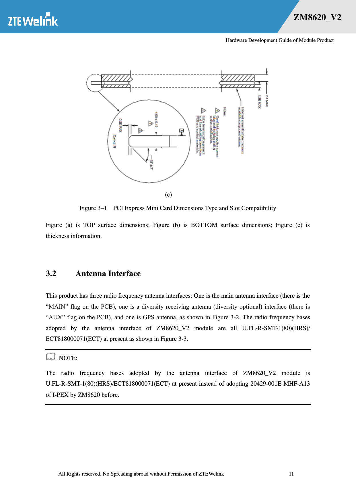
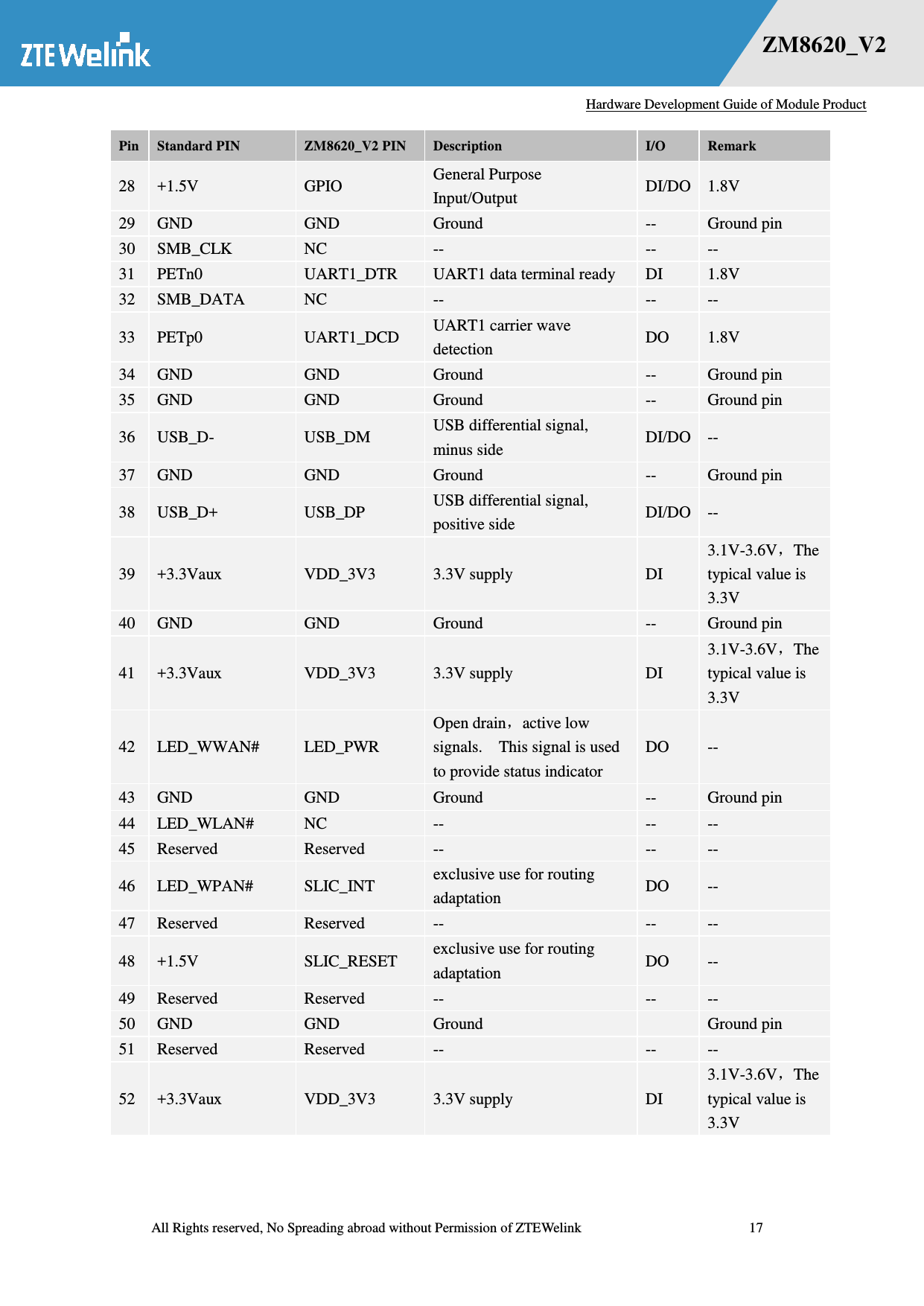
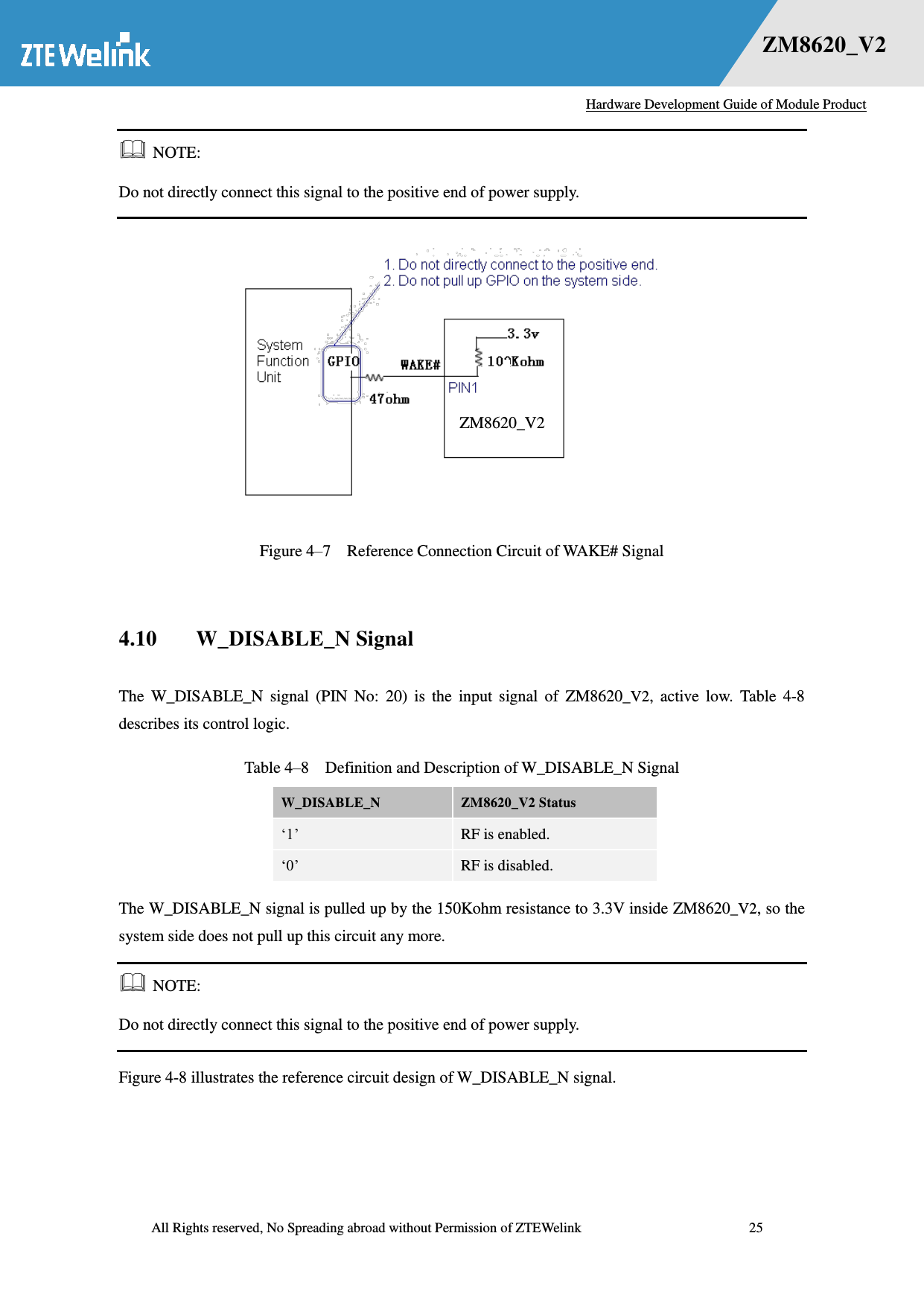
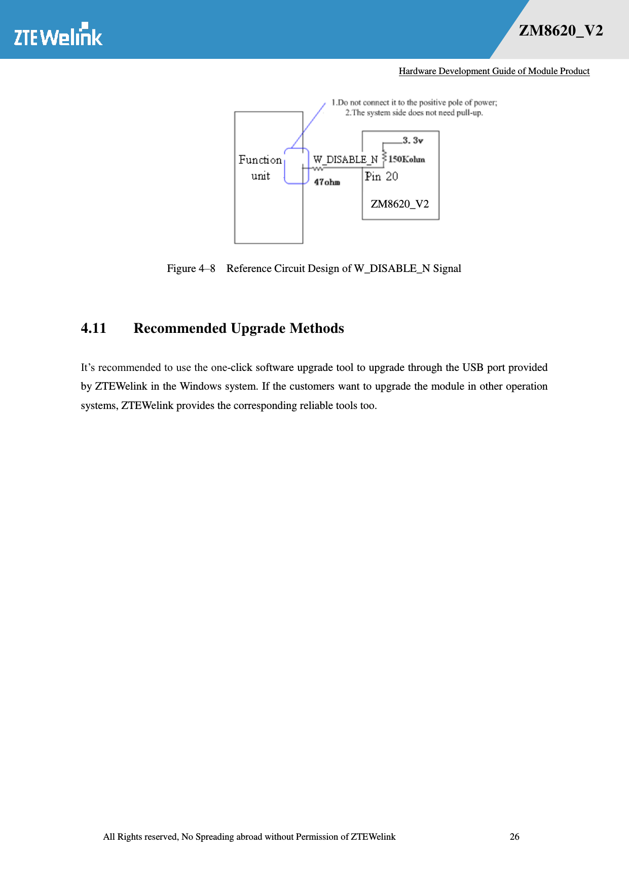
ZTE ZM8620 LTE Wireless Data Terminal User Manual
ZTE Corporation LTE Wireless Data Terminal Users Manual
UserManual.wiki
>
ZTE
>
ZM8620 User Manual
User Manual
Navigation menu
Upload a User Manual
Namespaces
Wiki Guide
HTML
PDF
Info
Views
User Manual
Discussion / Help
Navigation
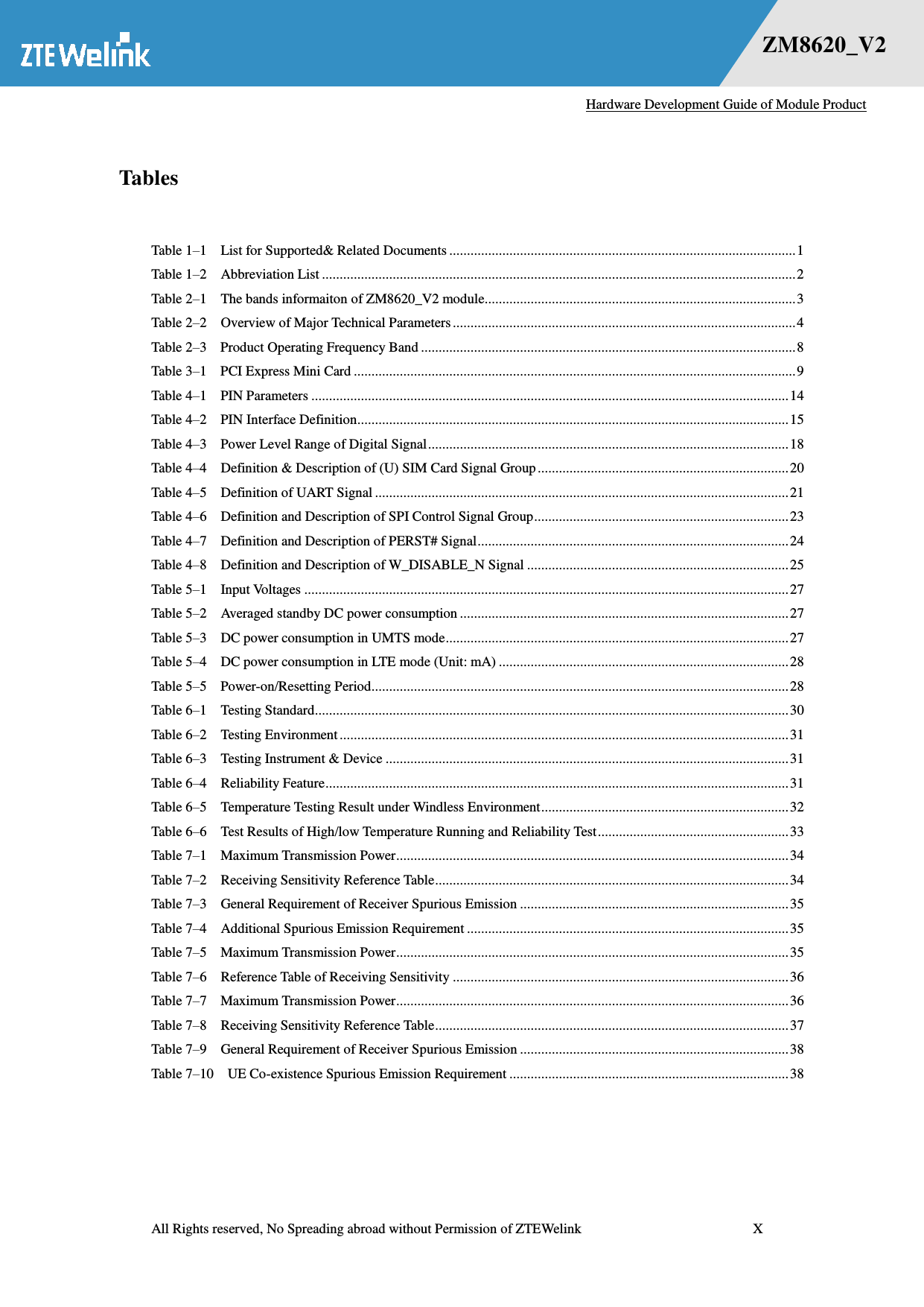
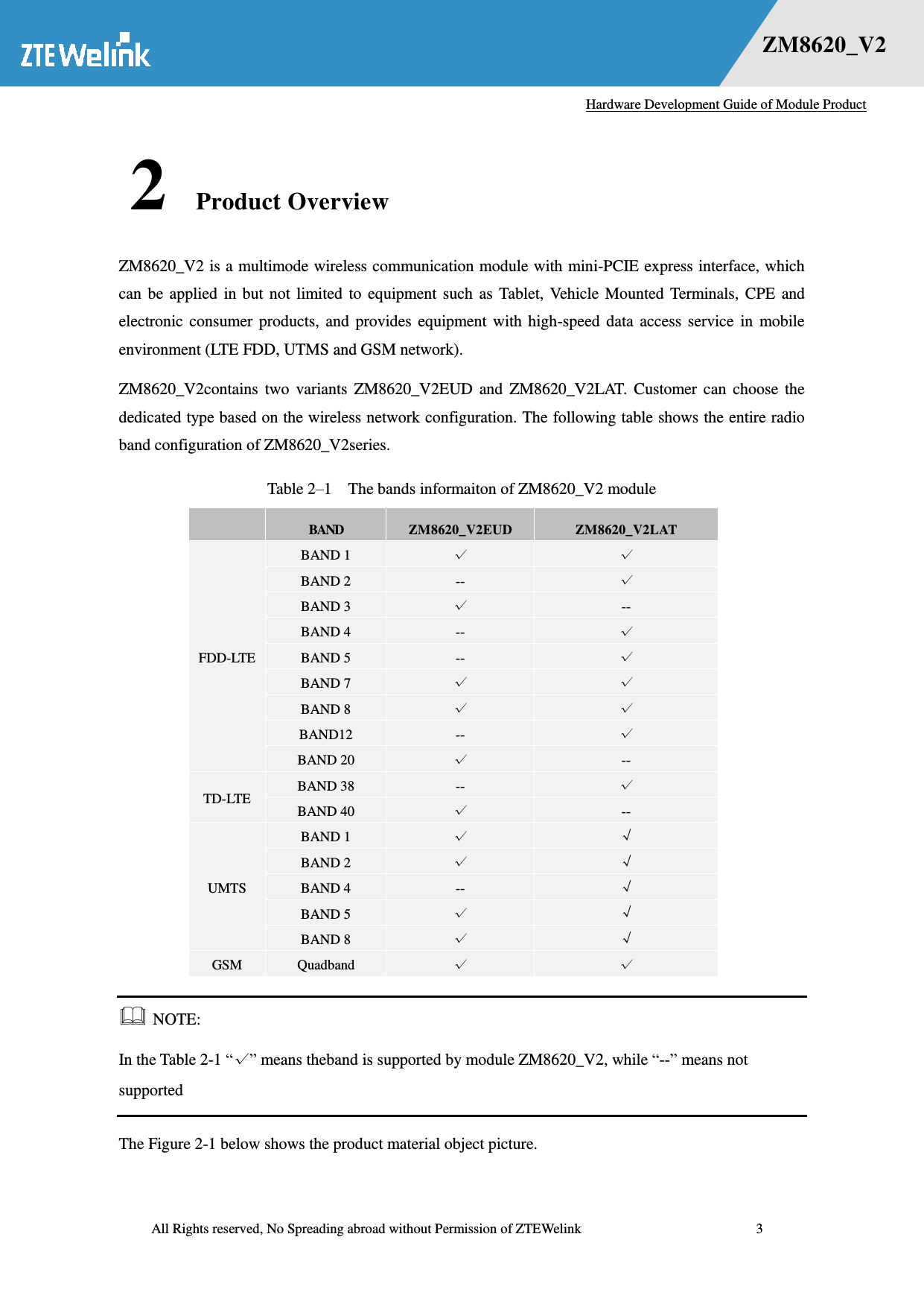
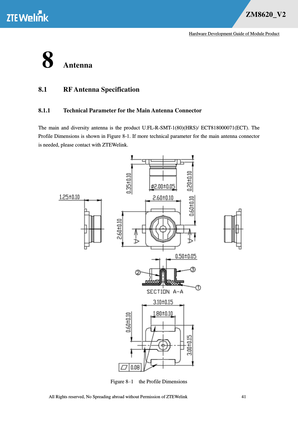
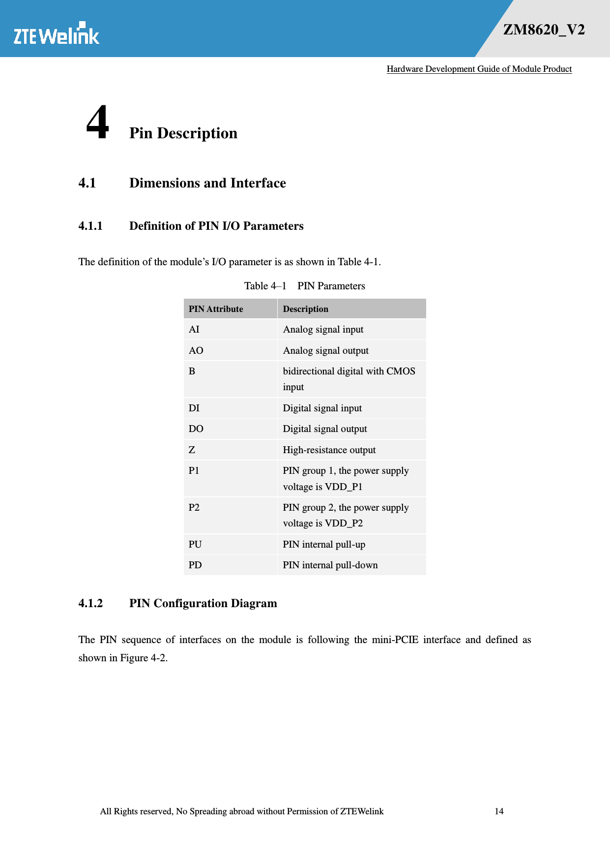
![Hardware Development Guide of Module Product All Rights reserved, No Spreading abroad without Permission of ZTEWelink 12 错误!未找到用源。 ZM8620_V2 Figure 3–2 Antenna Interface Flag Diagram (with Diversity) Figure 3–3 Radio Frequency Interface Test Base This product antenna is placed on the side of the system board. If this product is embedded in a notebook, place it on the top of the LCD screen. 3.3 Thermal Design The thermal design of this product strictly complies with the specification [PCI Express Mini Card Electromechanical Specification Revision 1.2, October 26, 2007], and distributes the heat source evenly, and has excellent heat dissipating design. As the maximum power consumption of the overall system is very high when transmitting, if it is impossible to ensure the temperature of ZM8620_V2 less than 60°C, the rise of the overall system temperature will lead to the performance degradation of ZM8620_V2, or even not operate normally. In order to ensure product performance, safety and stability, the following proposals are provided for the main board design: (a) the module far away from the switch power and high-speed signal cable as much as](https://usermanual.wiki/ZTE/ZM8620/User-Guide-2430423-Page-23.png)
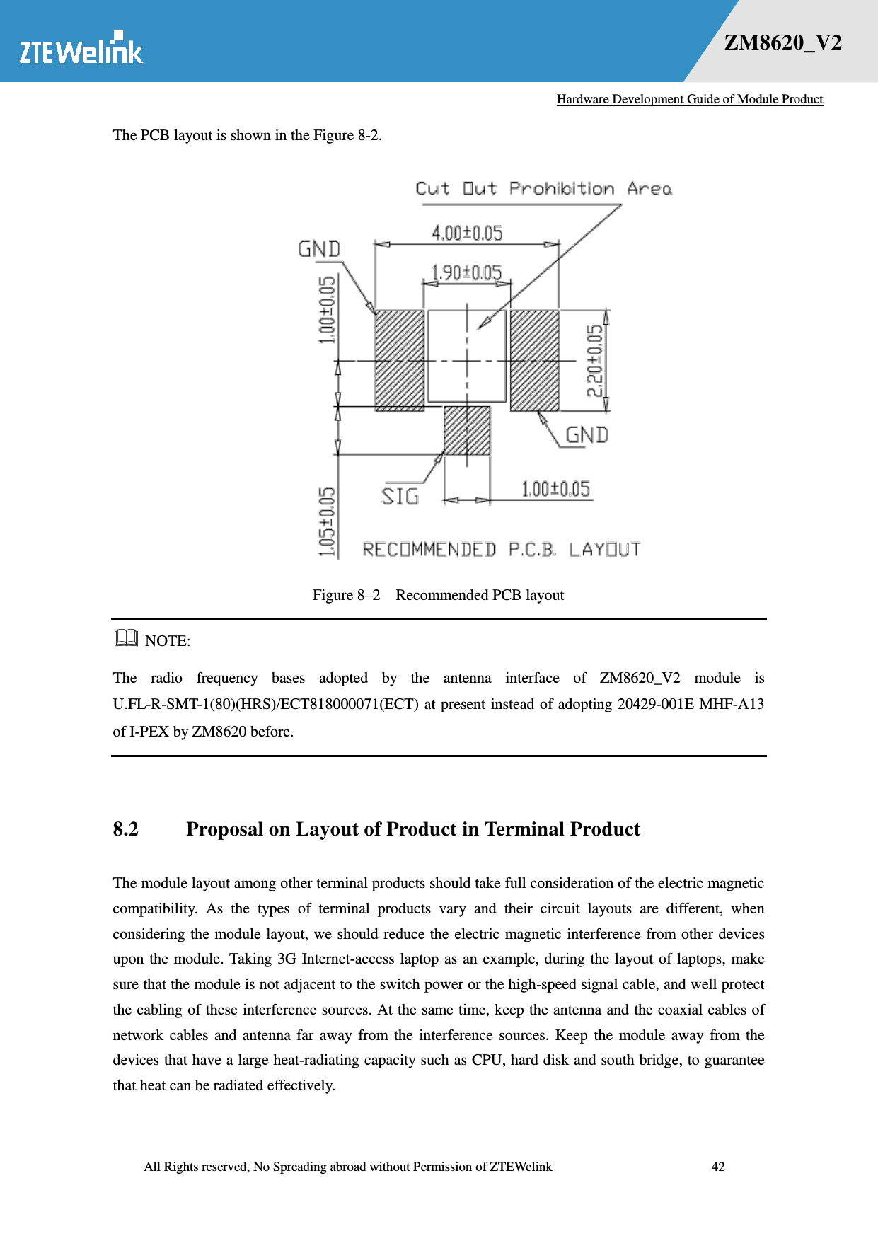
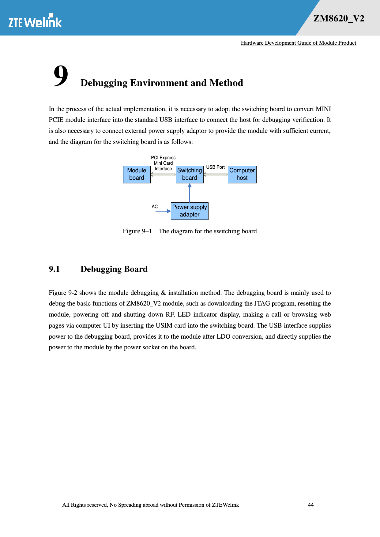
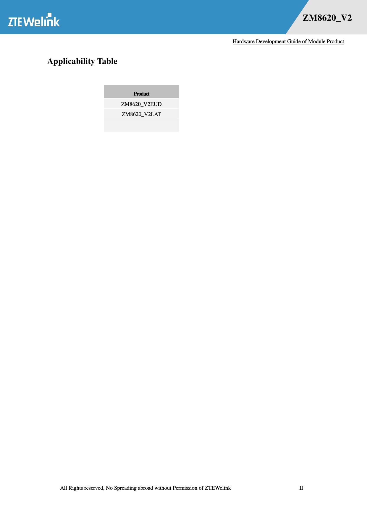
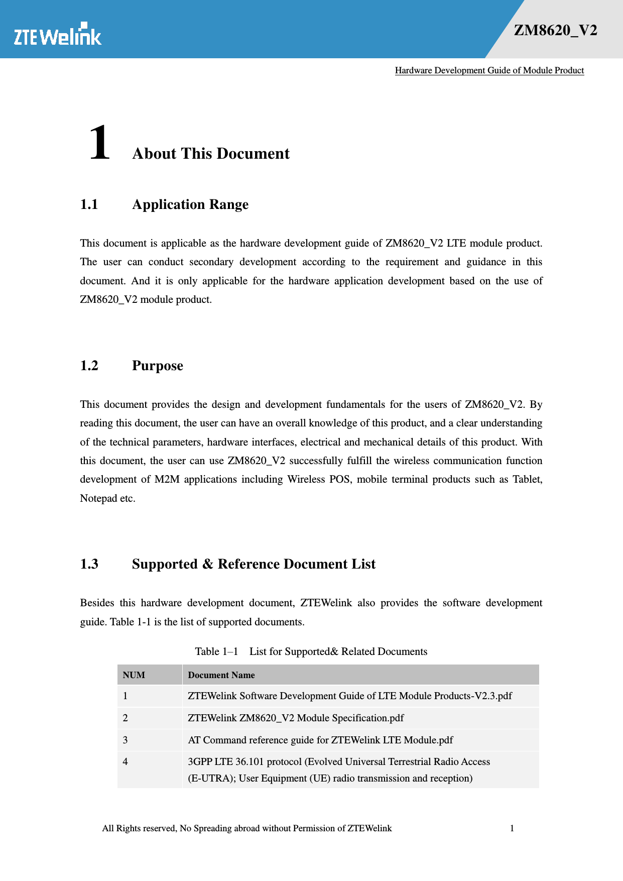
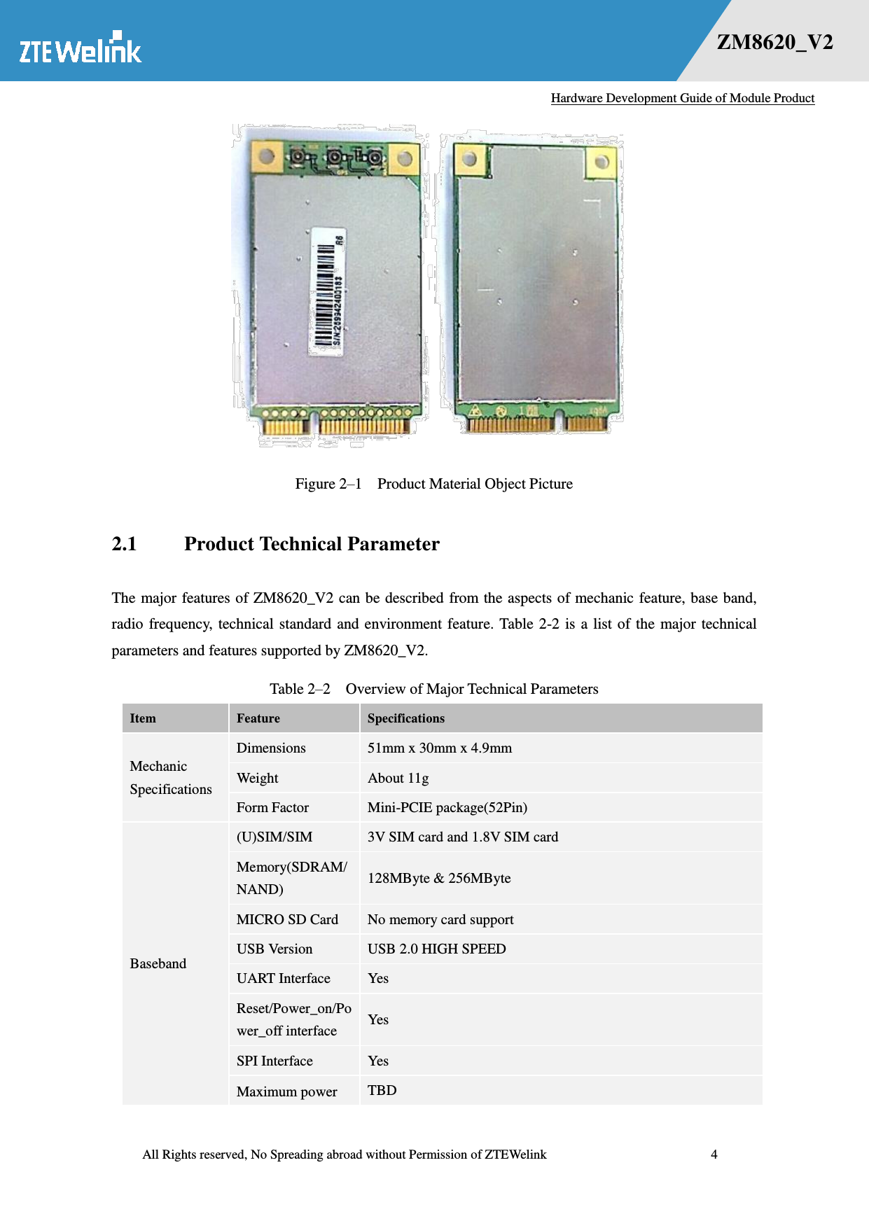
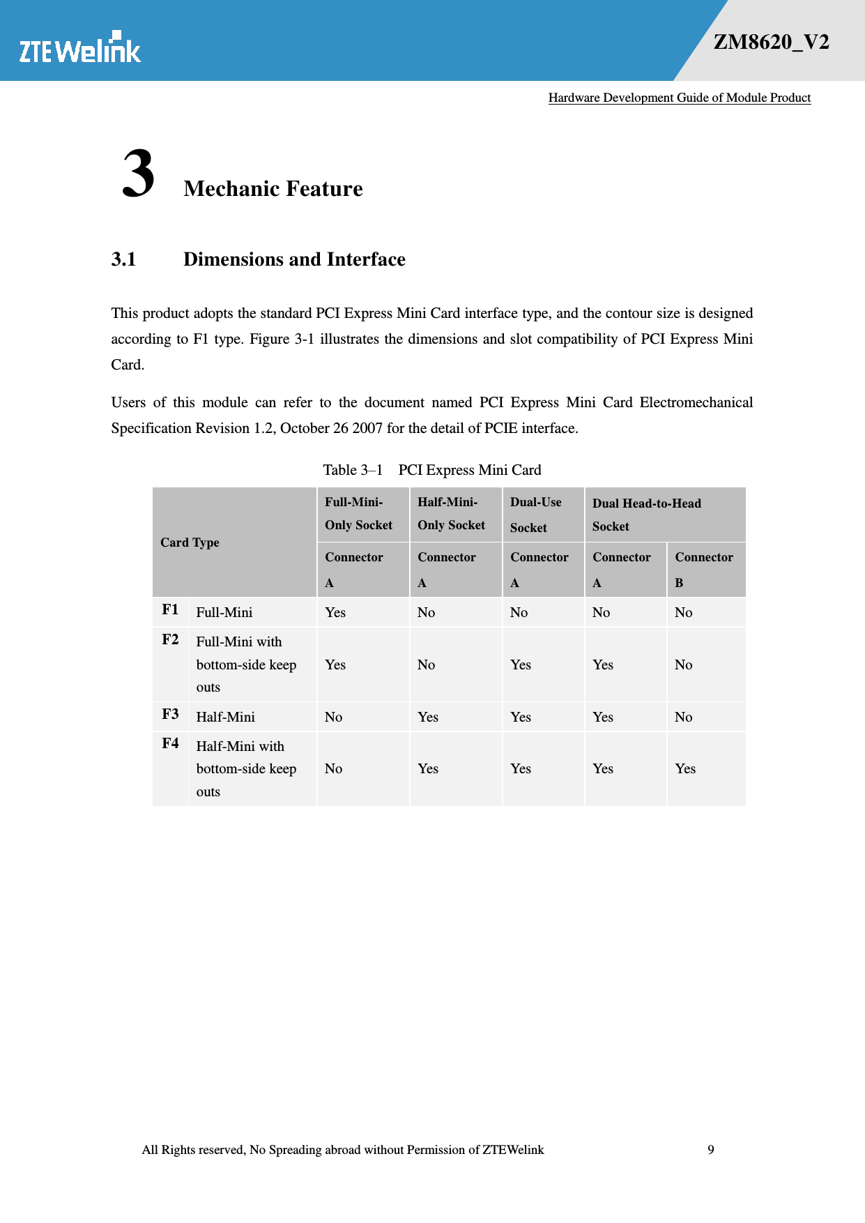
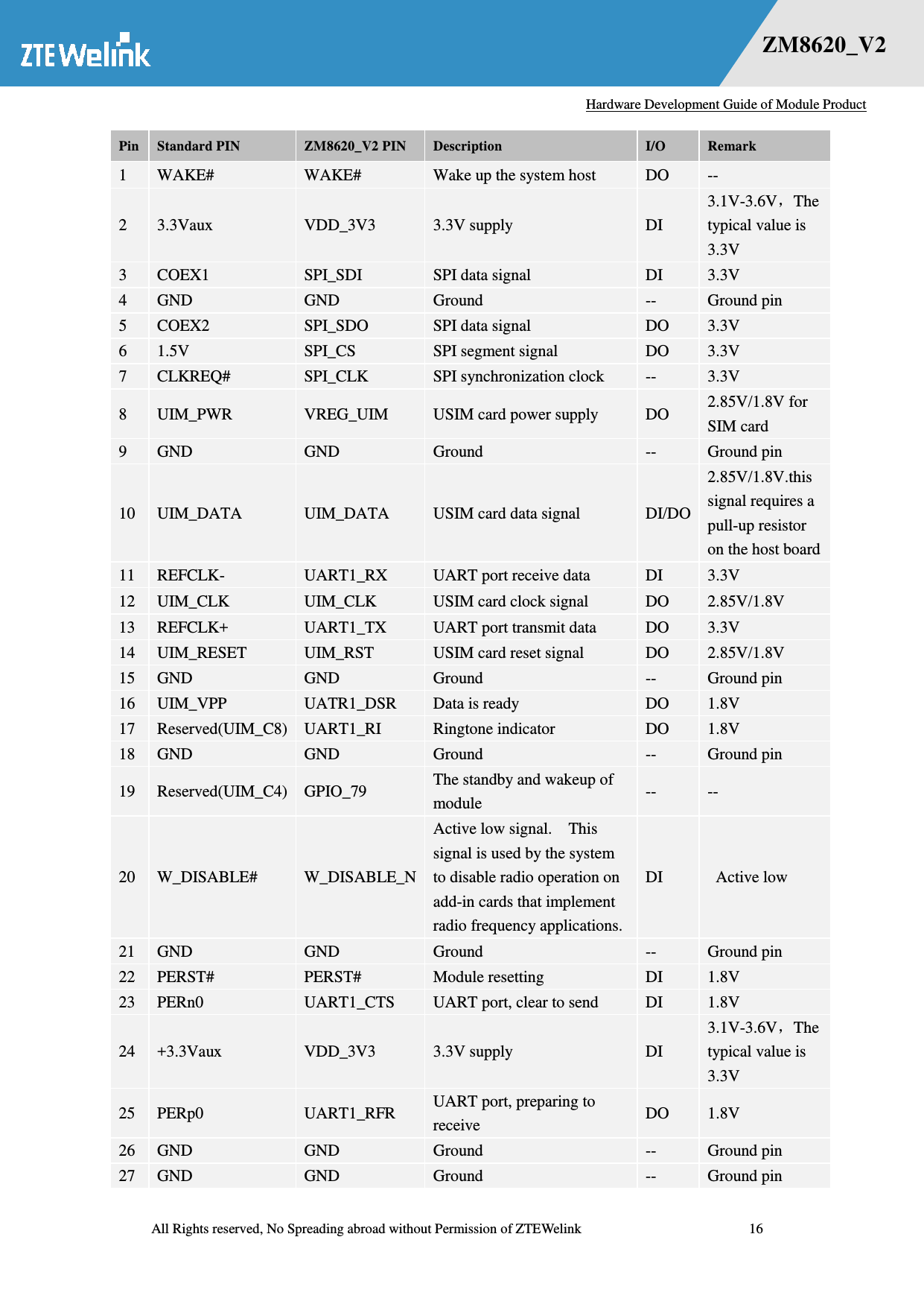
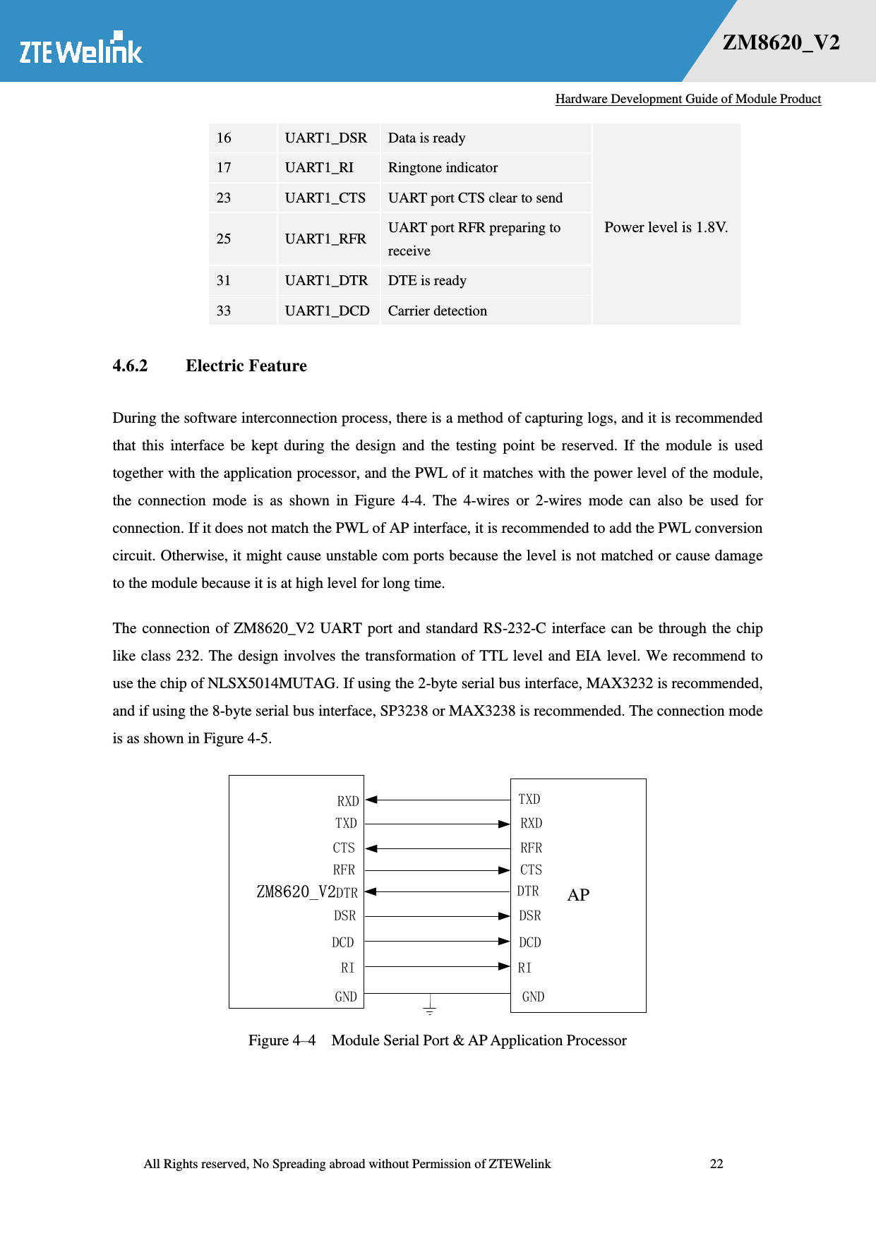
![Hardware Development Guide of Module Product All Rights reserved, No Spreading abroad without Permission of ZTEWelink 15 错误!未找到用源。 ZM8620_V2 Figure 4–1 PIN Distribution Diagram 123579111315171921232527293133353739414345495146810121416182022242628303234363840424446485052VDD_3V3VREG_UIMUIM_ DATAUIM_ CLKUIM_ RSTUART1_DSRW_DISABLE_NPERST#VDD_3V3USB_ DMUSB_ DPVDD_3V3VDD_3V3 LED_ PWRVDD_3V347GNDSPI_CSGNDGNDGPIONCGNDGNDNCSLIC_INTSLIC_RESETGNDWAKE #SPI_SDISPI_SDOSPI_CLKGNDGNDGNDGNDGNDGNDGNDUART1_RXUART1_RIGPIO_79UART1_CTSUART1_RFRUART1_DTRGNDRESERVEDRESERVEDRESERVEDRESERVEDCOEX1COEX2CLKREQ*GND[1]REFCLK-REFCLK+GND[2]RESERVED5_UIM_C8RESERVED4_UIM_C4GND[4]PERN0PERP0GND[6]GND[7]PETN0PETP0GND[9]GND[10]3V3VAUX[2]3V3VAUX[3]GND[12]RESERVED3RESERVED2RESERVED0RESERVED13V3VAUX[0]GND[0]1V5[0]UIM_PWRUIM_DATAUIM_CLKUIM_RESETUIM_VPPW_DISABLE*PERST*3V3VAUX[1]GND[5]1V5[1]SMB_CLKSMB_DATAGND[8]USB_D+LED_WWAN*LED_WLAN*LED_WPAN*1V5[2]GND[13]3V3VAUX[4]ZM8620_V2USB_D-GND[11]GND[3]UART1_DCDUART1_TXNC Figure 4–2 PIN Configuration Diagram 4.1.3 PIN Description Table 4–2 PIN Interface Definition](https://usermanual.wiki/ZTE/ZM8620/User-Guide-2430423-Page-26.png)
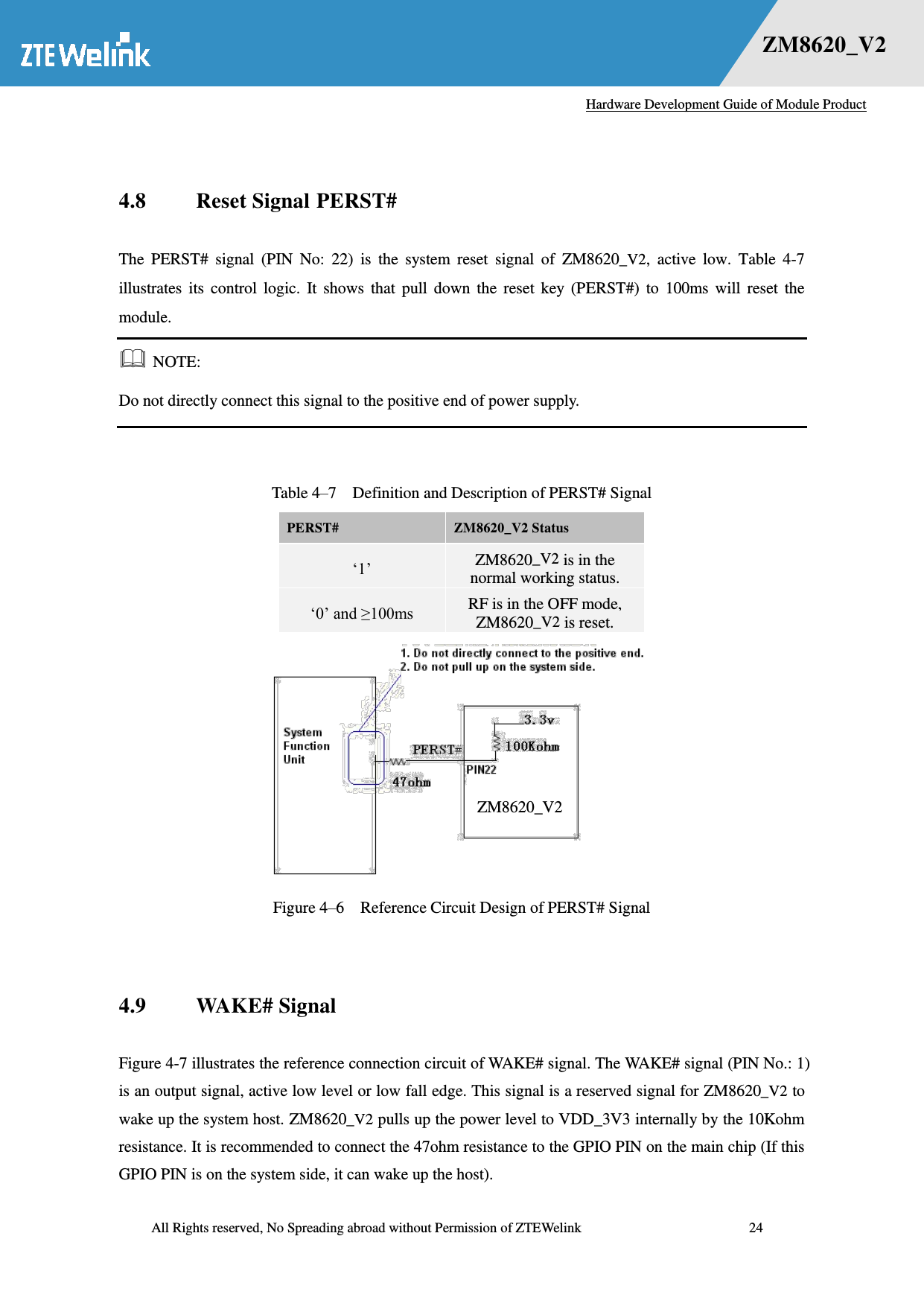
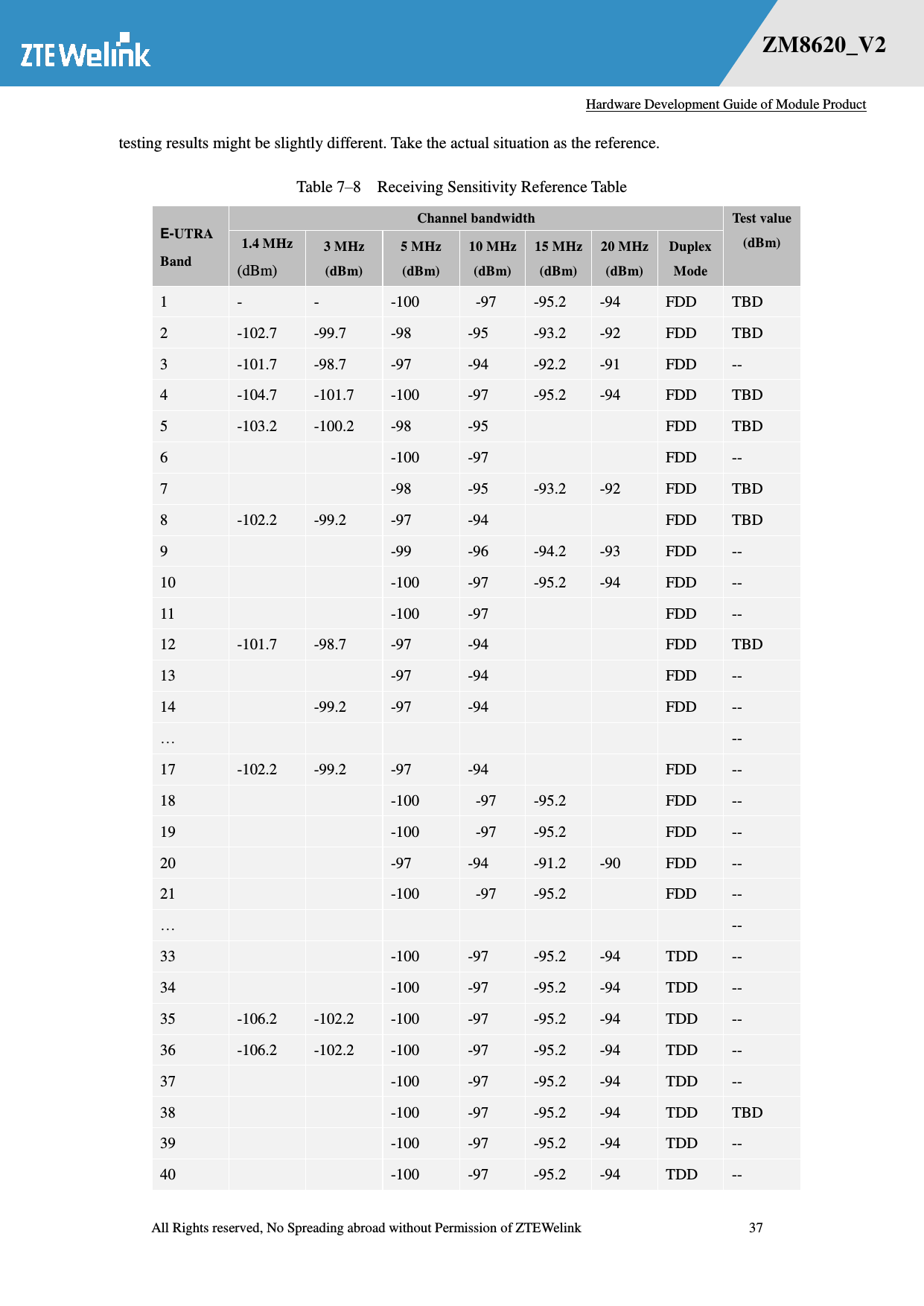
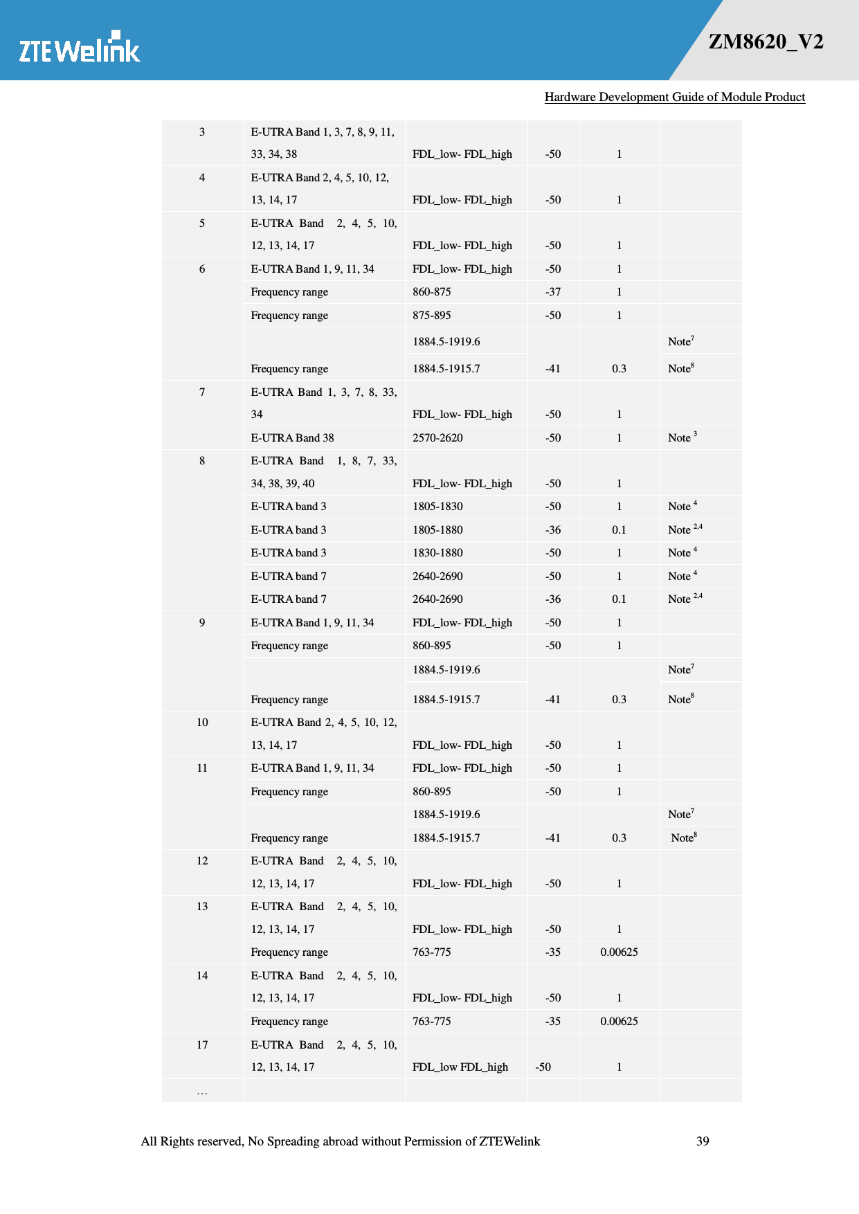
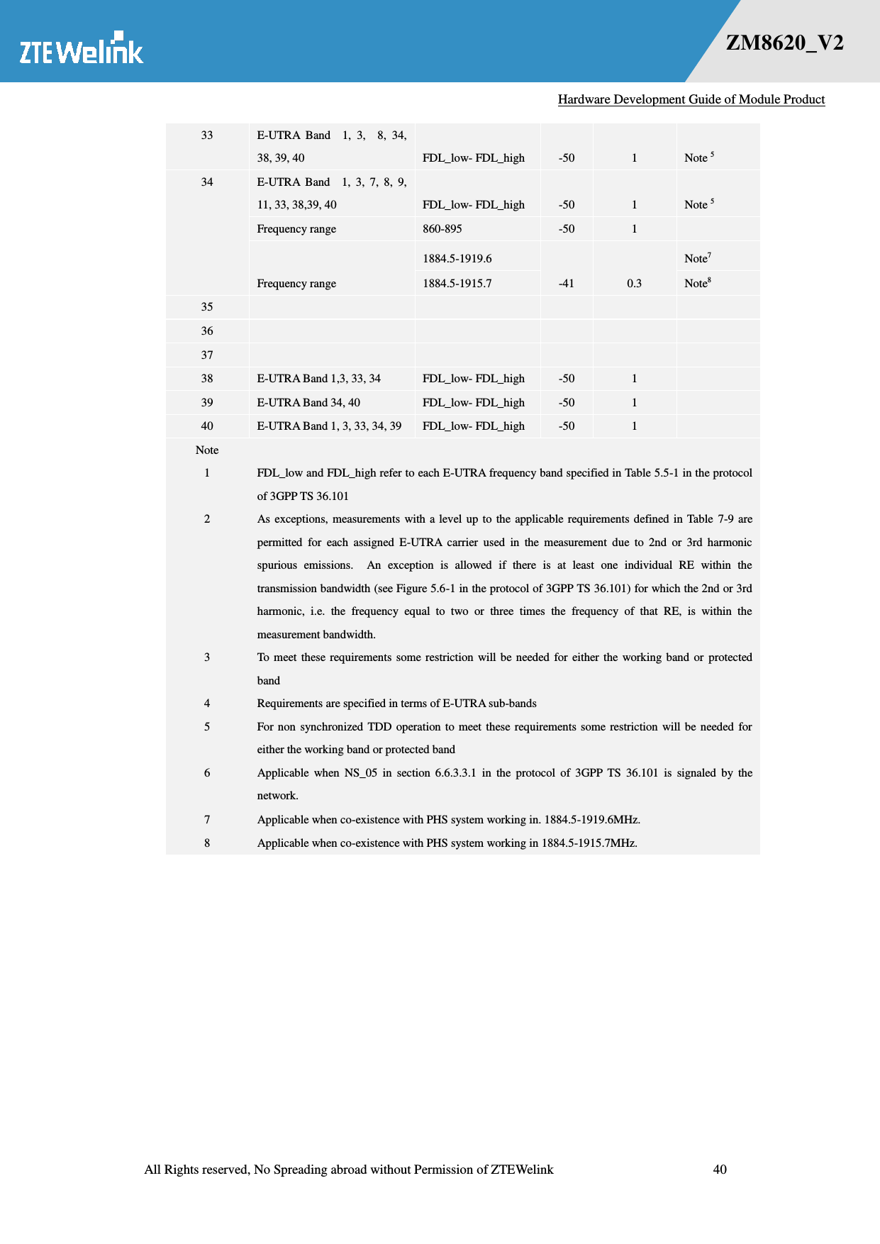
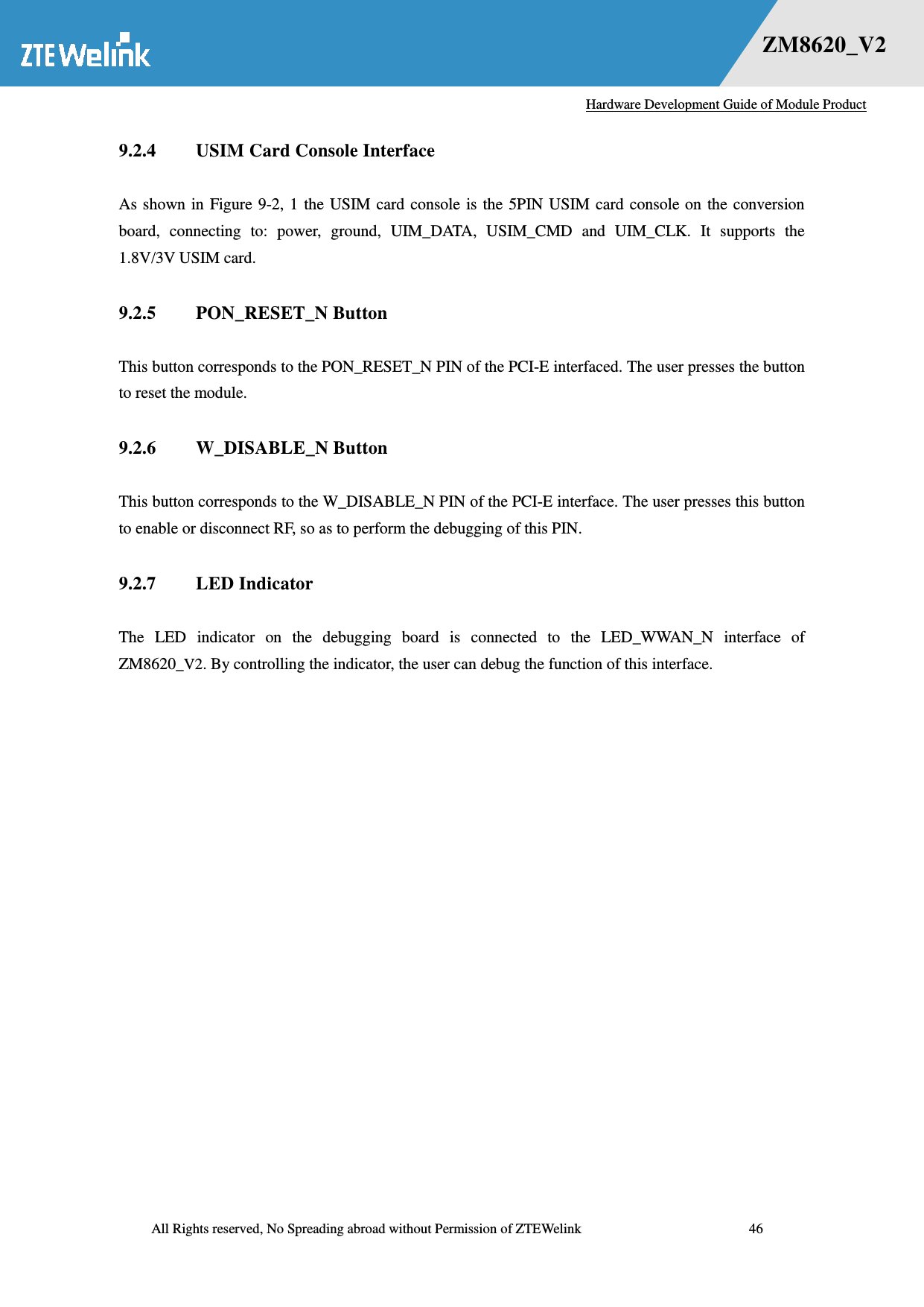
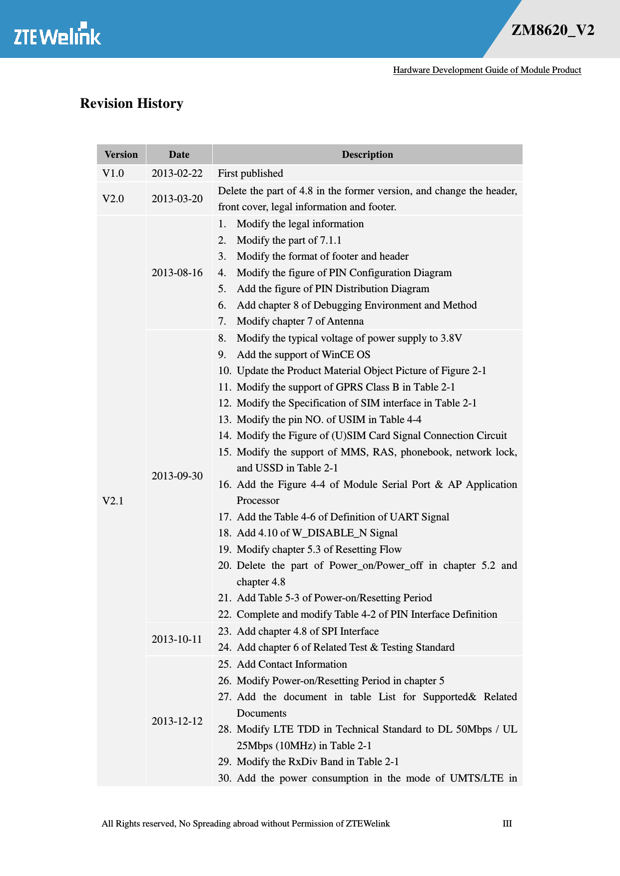
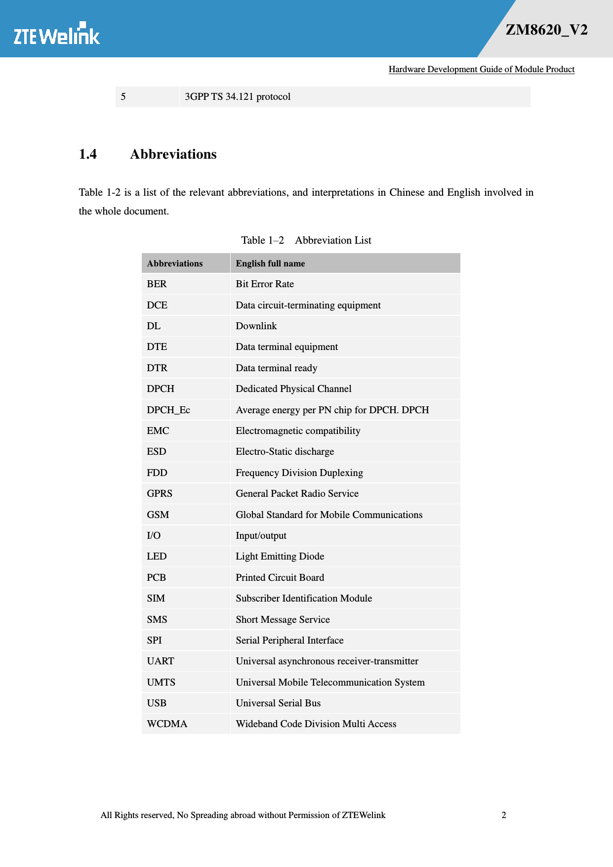
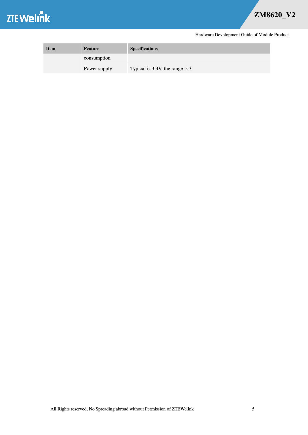
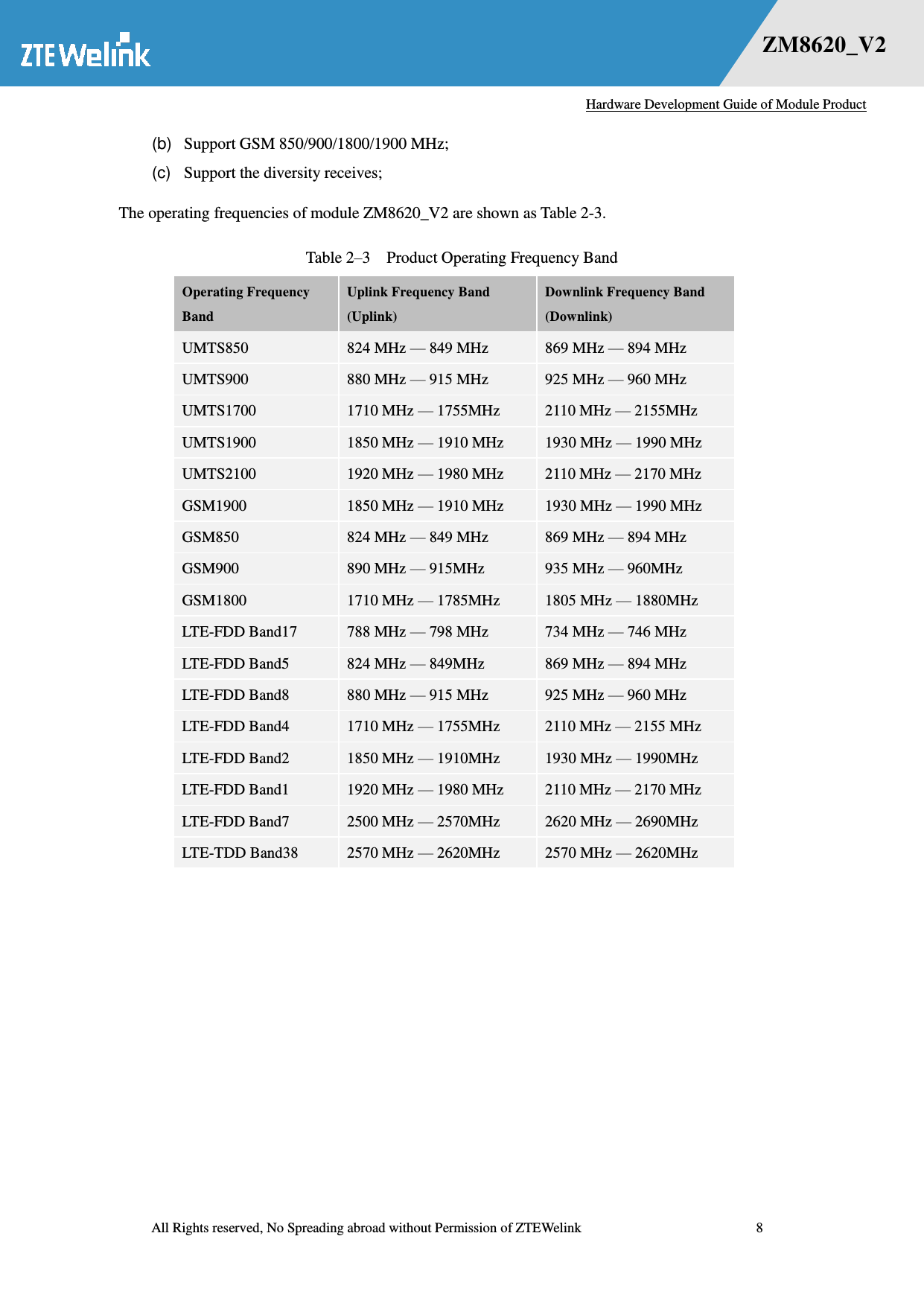
![Hardware Development Guide of Module Product All Rights reserved, No Spreading abroad without Permission of ZTEWelink 38 错误!未找到用源。 ZM8620_V2 41 [-100] [-97] [-95.2] [-94] TDD -- Note 1: The transmitter shall be set to maximum output power level as defined in clause 6.2.5 in the protocol of 3GPP TS 36.101 Note 2: Reference measurement channel is specified A.3.2 with one sided dynamic OCNG Pattern OP.1 FDD/TDD as described in Annex A.5.1.1/A.5.2.1 in the protocol of 3GPP TS 36.101 Note 3: The signal power is specified per port Note 4: For the UE which supports both Band 3 and Band 9 the reference sensitivity level of Band 3 + 0.5 dB is applicable for band 9 Note 5: For the UE which supports both Band 11 and Band 21 the reference sensitivity level is FFS. 7.3.3 Spurious Specification Spurious emission meets 3GPP TS 36.101 protocol requirement. The receiver spurious emission power refers to the spurious power generated or amplified by the module, which is tested from the antenna connector. The spurious emission shall meet the requirement of Table 7-9 and Table 7-10: Table 7–9 General Requirement of Receiver Spurious Emission Frequency range Maximum level Measurement bandwidth 9 kHz f < 150 kHz -36 dBm 1 kHz 150 kHz f < 30 MHz -36 dBm 10 kHz 30 MHz f < 1000 MHz -36 dBm 100 kHz 1 GHz f < 12.75 GHz -30 dBm 1 MHz Table 7–10 UE Co-existence Spurious Emission Requirement E-UTRA Band Spurious emission Protected band Frequency range (MHz) Level (dBm) Bandwidth (MHz) Comment 1 E-UTRA Band 1, 3, 7, 8, 9, 11, 34, 38, 40 FDL_low - FDL_high -50 1 Frequency range 860-895 -50 1 Frequency range 1884.5-1919.6 -41 0.3 Note6,Note7 1884.5-1915.7 Note 6, Note8 E-UTRA band 33 1900-1920 -50 1 Note 3 E-UTRA band 39 1880-1920 -50 1 Note 3 2 E-UTRA Band 2, 4, 5, 10, 12, 13, 14, 17 FDL_low- FDL_high -50 1](https://usermanual.wiki/ZTE/ZM8620/User-Guide-2430423-Page-49.png)