ZTE ZM8620 LTE Wireless Data Terminal User Manual
ZTE Corporation LTE Wireless Data Terminal Users Manual
ZTE >
User Manual

Hardware Development Guide of
Module Product
Welink Your Smart
Version 2.3, 2014-04-15
ZM8620_V2

Hardware Development Guide of Module Product
All Rights reserved, No Spreading abroad without Permission of ZTEWelink I
错误!未找到
用源。
ZM8620_V2
Legal Information
By receiving the document from Shenzhen ZTEWelink Technology Co., Ltd (shortly referred to as
ZTEWelink), you are deemed to have agreed to the following terms. If you don‘t agree to the following
terms, please stop using the document.
Copyright © 2013 Shenzhen ZTEWelink Technology Co., Ltd. All rights reserved. The document
contains ZTEWelink‘s proprietary information. Without the prior written permission of ZTEWelink, no
entity or individual is allowed to reproduce, transfer, distribute, use and disclose this document or any
image, table, data or other information contained in this document.
As the wholly-owned subsidiaries of ZTE, ZTEWelink is the professional company engaging in R&D,
manufacture and sales of wireless module product. is the registered trademark of
ZTEWelink. The name and logo of ZTEWelink are ZTEWelink‘s trademark or registered trademark.
Meanwhile, ZTEWelink is a wholly-owned subsidiary of ZTE Corporation, and is granted to use ZTE
Corporation‘s registered trademark. The other products or company names mentioned in this document
are the trademark or registered trademark of their respective owner. Without the prior written permission
of ZTEWelink or the third-party oblige, no one is allowed to read this document.
The product meets the design requirements of environmental protection and personal security. The
storage, use or disposal of products should abide by the product manual, relevant contract or the laws
and regulations of relevant country.
ZTEWelink reserves the right to make modifications on the product described in this document without
prior notice, and keeps the right to revise or retrieve the document any time.
If you have any question about the manual, please consult the company or its distributors promptly.

Hardware Development Guide of Module Product
All Rights reserved, No Spreading abroad without Permission of ZTEWelink II
错误!未找到
用源。
ZM8620_V2
Applicability Table
Product
ZM8620_V2EUD
ZM8620_V2LAT

Hardware Development Guide of Module Product
All Rights reserved, No Spreading abroad without Permission of ZTEWelink III
错误!未找到
用源。
ZM8620_V2
Revision History
Version
Date
Description
V1.0
2013-02-22
First published
V2.0
2013-03-20
Delete the part of 4.8 in the former version, and change the header,
front cover, legal information and footer.
V2.1
2013-08-16
1. Modify the legal information
2. Modify the part of 7.1.1
3. Modify the format of footer and header
4. Modify the figure of PIN Configuration Diagram
5. Add the figure of PIN Distribution Diagram
6. Add chapter 8 of Debugging Environment and Method
7. Modify chapter 7 of Antenna
2013-09-30
8. Modify the typical voltage of power supply to 3.8V
9. Add the support of WinCE OS
10. Update the Product Material Object Picture of Figure 2-1
11. Modify the support of GPRS Class B in Table 2-1
12. Modify the Specification of SIM interface in Table 2-1
13. Modify the pin NO. of USIM in Table 4-4
14. Modify the Figure of (U)SIM Card Signal Connection Circuit
15. Modify the support of MMS, RAS, phonebook, network lock,
and USSD in Table 2-1
16. Add the Figure 4-4 of Module Serial Port & AP Application
Processor
17. Add the Table 4-6 of Definition of UART Signal
18. Add 4.10 of W_DISABLE_N Signal
19. Modify chapter 5.3 of Resetting Flow
20. Delete the part of Power_on/Power_off in chapter 5.2 and
chapter 4.8
21. Add Table 5-3 of Power-on/Resetting Period
22. Complete and modify Table 4-2 of PIN Interface Definition
2013-10-11
23. Add chapter 4.8 of SPI Interface
24. Add chapter 6 of Related Test & Testing Standard
2013-12-12
25. Add Contact Information
26. Modify Power-on/Resetting Period in chapter 5
27. Add the document in table List for Supported& Related
Documents
28. Modify LTE TDD in Technical Standard to DL 50Mbps / UL
25Mbps (10MHz) in Table 2-1
29. Modify the RxDiv Band in Table 2-1
30. Add the power consumption in the mode of UMTS/LTE in

Hardware Development Guide of Module Product
All Rights reserved, No Spreading abroad without Permission of ZTEWelink IV
错误!未找到
用源。
ZM8620_V2
Version
Date
Description
chapter 5.1
31. Modify the antenna interface to MHF-A13 of I-PEX
V2.2
2014-03-06
1. Modify the typical voltage of power supply to 3.3V,and the
range to 3.1-3.6V
2. Modify the the Profile Dimensions in Figure 8-1 and The PCB
layout is shown in the Figure 8-2.
3. Modify the antenna interface to U.FL-R-SMT-1(80)(HRS)/
ECT818000071(ECT)
4. Modify the pins in chapter 4.1
5. Modify the chapter 4.6 of UART interface
6. Update the format and template of the document
7. Update the legal information of this document
8. Update the Product Material Object Picture in Figure 2-1
V2.3
2014-04-15
1. Update the document as the hardware development guide of
module ZM8620_V2
2. Add the difference between the module ZM8620_V2 and
ZM8620.
3. Update the bands information of two variants
ZM8620_V2EUD and ZM8620_V2LAT
4. Modify the Figure in chapter of UART electric feature
5. Add the chapter of 10 and 11
6. Update the Overview of Major Technical Parameters in Table
2–2
Note: Because of ZTEWelink ZM8620_V2 module is still under revision to improve its performances,
the present document could be subject to revisions without notice.

Hardware Development Guide of Module Product
All Rights reserved, No Spreading abroad without Permission of ZTEWelink V
错误!未找到
用源。
ZM8620_V2
Contact Information
Post
9/F, Tower A, Hans Innovation Mansion,
North Ring Rd., No.9018, Hi-Tech Industrial Park,
Nanshan District, Shenzhen, P.R.China.
Web
www.ztewelink.com
Phone
+86-755-86360200-8679
E-Mail
ztewelink@zte.com.cn
Note: Consult our website for up-to-date product descriptions, documentation, application notes,
firmware upgrades, troubleshooting tips, and press releases
Besides, ZTEWelink provides various technical support ways to the customers, such as support by phone,
website, instant messaging, E-mail and on-site.

Hardware Development Guide of Module Product
All Rights reserved, No Spreading abroad without Permission of ZTEWelink VI
错误!未找到
用源。
ZM8620_V2
Contents
LEGAL INFORMATION ....................................................................................................................................... I
1 ABOUT THIS DOCUMENT ..................................................................................................................... 1
1.1 Application Range ................................................................................................................................. 1
1.2 Purpose ................................................................................................................................................ 1
1.3 Supported & Reference Document List .................................................................................................... 1
1.4 Abbreviations ....................................................................................................................................... 2
2 PRODUCT OVERVIEW ........................................................................................................................... 3
2.1 Product Technical Parameter .................................................................................................................. 4
2.2 Function Overview ................................................................................................................................ 7
2.2.1 Baseband Function .................................................................................................................... 7
2.2.2 Radio Frequency Function ......................................................................................................... 7
3 MECHANIC FEATURE ............................................................................................................................ 9
3.1 Dimensions and Interface ....................................................................................................................... 9
3.2 Antenna Interface ................................................................................................................................ 11
3.3 Thermal Design .................................................................................................................................. 12
4 PIN DESCRIPTION ................................................................................................................................ 14
4.1 Dimensions and Interface ..................................................................................................................... 14
4.1.1 Definition of PIN I/O Parameters .............................................................................................. 14
4.1.2 PIN Configuration Diagram ...................................................................................................... 14
4.1.3 PIN Description ........................................................................................................................ 15
4.2 Feature of Interface Power Level .......................................................................................................... 18
4.2.1 Power Level of IO Interface ...................................................................................................... 18
4.3 Power Interface ................................................................................................................................... 19
4.3.1 Description of Power PINs ....................................................................................................... 19
4.3.2 Requirement of Power Supply .................................................................................................. 19
4.4 (U)SIM Card Interface ......................................................................................................................... 19
4.4.1 Description of PINs ................................................................................................................... 19

Hardware Development Guide of Module Product
All Rights reserved, No Spreading abroad without Permission of ZTEWelink VII
错误!未找到
用源。
ZM8620_V2
4.4.2 Electric Feature ........................................................................................................................ 20
4.5 USB2.0 Interface ................................................................................................................................ 20
4.5.1 Description of PINs ................................................................................................................... 20
4.5.2 Electric Feature ........................................................................................................................ 21
4.6 UART Interface .................................................................................................................................. 21
4.6.1 Description of PINs ................................................................................................................... 21
4.6.2 Electric Feature ........................................................................................................................ 22
4.7 SPI Interface ....................................................................................................................................... 23
4.8 Reset Signal PERST# .......................................................................................................................... 24
4.9 WAKE# Signal ................................................................................................................................... 24
4.10 W_DISABLE_N Signal ....................................................................................................................... 25
4.11 Recommended Upgrade Methods ......................................................................................................... 26
5 ELECTRIC FEATURE ........................................................................................................................... 27
5.1 Power Feature ..................................................................................................................................... 27
5.1.1 Power Supply ........................................................................................................................... 27
5.1.2 Working Current ....................................................................................................................... 27
5.2 Power-on/Resetting Flow ..................................................................................................................... 28
5.3 Resetting Flow .................................................................................................................................... 29
6 RELATED TEST & TESTING STANDARD ........................................................................................... 30
6.1 Testing Reference ................................................................................................................................ 30
6.2 Description of Testing Environment ...................................................................................................... 30
6.3 Reliability Testing Environment ............................................................................................................ 31
6.4 Reliability Test Result .......................................................................................................................... 32
7 RF SPECIFICATIONS ........................................................................................................................... 34
7.1 Technical Specification for UMTS Mode Radio Frequency ..................................................................... 34
7.1.1 Maximum Transmission Power................................................................................................. 34
7.1.2 Receiving Sensitivity ................................................................................................................ 34
7.1.3 Spurious Specification .............................................................................................................. 35
7.2 Technical Specification of GSM Mode Radio Frequency ......................................................................... 35

Hardware Development Guide of Module Product
All Rights reserved, No Spreading abroad without Permission of ZTEWelink VIII
错误!未找到
用源。
ZM8620_V2
7.2.1 Maximum Transmission Power................................................................................................. 35
7.2.2 Receiving Sensitivity ................................................................................................................ 36
7.3 Technical Specification of LTE Mode Radio Frequency .......................................................................... 36
7.3.1 Maximum Transmission Power................................................................................................. 36
7.3.2 Receiving Sensitivity ................................................................................................................ 36
7.3.3 Spurious Specification .............................................................................................................. 38
8 ANTENNA ............................................................................................................................................. 41
8.1 RF Antenna Specification ..................................................................................................................... 41
8.1.1 Technical Parameter for the Main Antenna Connector ............................................................. 41
8.2 Proposal on Layout of Product in Terminal Product ................................................................................ 42
8.3 Antenna Dimensions and Location ........................................................................................................ 43
8.4 Diversity Antenna Design .................................................................................................................... 43
9 DEBUGGING ENVIRONMENT AND METHOD .................................................................................... 44
9.1 Debugging Board ................................................................................................................................ 44
9.2 Interfaces on Debugging Board............................................................................................................. 45
9.2.1 JTAG Interface ......................................................................................................................... 45
9.2.2 USB Interface ........................................................................................................................... 45
9.2.3 Power-supply Interface ............................................................................................................. 45
9.2.4 USIM Card Console Interface .................................................................................................. 46
9.2.5 PON_RESET_N Button ............................................................................................................ 46
9.2.6 W_DISABLE_N Button ............................................................................................................. 46
9.2.7 LED Indicator............................................................................................................................ 46
10 PACKAGE SYSTEM .............................................................................................................................. 47
11 SAFETY INFORMATION ....................................................................................................................... 48

Hardware Development Guide of Module Product
All Rights reserved, No Spreading abroad without Permission of ZTEWelink IX
错误!未找到
用源。
ZM8620_V2
Figures
Figure 2–1 Product Material Object Picture .............................................................................................................. 4
Figure 2–2 System Connection Diagram ................................................................................................................... 7
Figure 3–1 PCI Express Mini Card Dimensions Type and Slot Compatibility ........................................................ 11
Figure 3–2 Antenna Interface Flag Diagram (with Diversity) ................................................................................. 12
Figure 3–3 Radio Frequency Interface Test Base .................................................................................................... 12
Figure 4–1 PIN Distribution Diagram ..................................................................................................................... 15
Figure 4–2 PIN Configuration Diagram .................................................................................................................. 15
Figure 4–3 (U)SIM Card Signal Connection Circuit ............................................................................................... 19
Figure 4–4 Module Serial Port & AP Application Processor ................................................................................... 22
Figure 4–5 The connection of ZM8620_V2 UART and Standard RS-232-C interface ........................................... 23
Figure 4–6 Reference Circuit Design of PERST# Signal ........................................................................................ 24
Figure 4–7 Reference Connection Circuit of WAKE# Signal .................................................................................. 25
Figure 4–8 Reference Circuit Design of W_DISABLE_N Signal ........................................................................... 26
Figure 5–1 Module Reset Flow ............................................................................................................................... 29
Figure 8–1 the Profile Dimensions .......................................................................................................................... 41
Figure 8–2 Recommended PCB layout .................................................................................................................... 42
Figure 9–1 The diagram for the switching board ..................................................................................................... 44
Figure 9–2 Debugging Board .................................................................................................................................. 45
Figure 10–1 Package process of ZM8620_V2 modules .......................................................................................... 47

Hardware Development Guide of Module Product
All Rights reserved, No Spreading abroad without Permission of ZTEWelink X
错误!未找到
用源。
ZM8620_V2
Tables
Table 1–1 List for Supported& Related Documents .................................................................................................. 1
Table 1–2 Abbreviation List ...................................................................................................................................... 2
Table 2–1 The bands informaiton of ZM8620_V2 module........................................................................................ 3
Table 2–2 Overview of Major Technical Parameters ................................................................................................. 4
Table 2–3 Product Operating Frequency Band .......................................................................................................... 8
Table 3–1 PCI Express Mini Card ............................................................................................................................. 9
Table 4–1 PIN Parameters ....................................................................................................................................... 14
Table 4–2 PIN Interface Definition .......................................................................................................................... 15
Table 4–3 Power Level Range of Digital Signal ...................................................................................................... 18
Table 4–4 Definition & Description of (U) SIM Card Signal Group ....................................................................... 20
Table 4–5 Definition of UART Signal ..................................................................................................................... 21
Table 4–6 Definition and Description of SPI Control Signal Group ........................................................................ 23
Table 4–7 Definition and Description of PERST# Signal ........................................................................................ 24
Table 4–8 Definition and Description of W_DISABLE_N Signal .......................................................................... 25
Table 5–1 Input Voltages ......................................................................................................................................... 27
Table 5–2 Averaged standby DC power consumption ............................................................................................. 27
Table 5–3 DC power consumption in UMTS mode ................................................................................................. 27
Table 5–4 DC power consumption in LTE mode (Unit: mA) .................................................................................. 28
Table 5–5 Power-on/Resetting Period ...................................................................................................................... 28
Table 6–1 Testing Standard ...................................................................................................................................... 30
Table 6–2 Testing Environment ............................................................................................................................... 31
Table 6–3 Testing Instrument & Device .................................................................................................................. 31
Table 6–4 Reliability Feature ................................................................................................................................... 31
Table 6–5 Temperature Testing Result under Windless Environment ...................................................................... 32
Table 6–6 Test Results of High/low Temperature Running and Reliability Test ...................................................... 33
Table 7–1 Maximum Transmission Power ............................................................................................................... 34
Table 7–2 Receiving Sensitivity Reference Table .................................................................................................... 34
Table 7–3 General Requirement of Receiver Spurious Emission ............................................................................ 35
Table 7–4 Additional Spurious Emission Requirement ........................................................................................... 35
Table 7–5 Maximum Transmission Power ............................................................................................................... 35
Table 7–6 Reference Table of Receiving Sensitivity ............................................................................................... 36
Table 7–7 Maximum Transmission Power ............................................................................................................... 36
Table 7–8 Receiving Sensitivity Reference Table .................................................................................................... 37
Table 7–9 General Requirement of Receiver Spurious Emission ............................................................................ 38
Table 7–10 UE Co-existence Spurious Emission Requirement ............................................................................... 38

Hardware Development Guide of Module Product
All Rights reserved, No Spreading abroad without Permission of ZTEWelink 1
错误!未找到
用源。
ZM8620_V2
1 About This Document
1.1 Application Range
This document is applicable as the hardware development guide of ZM8620_V2 LTE module product.
The user can conduct secondary development according to the requirement and guidance in this
document. And it is only applicable for the hardware application development based on the use of
ZM8620_V2 module product.
1.2 Purpose
This document provides the design and development fundamentals for the users of ZM8620_V2. By
reading this document, the user can have an overall knowledge of this product, and a clear understanding
of the technical parameters, hardware interfaces, electrical and mechanical details of this product. With
this document, the user can use ZM8620_V2 successfully fulfill the wireless communication function
development of M2M applications including Wireless POS, mobile terminal products such as Tablet,
Notepad etc.
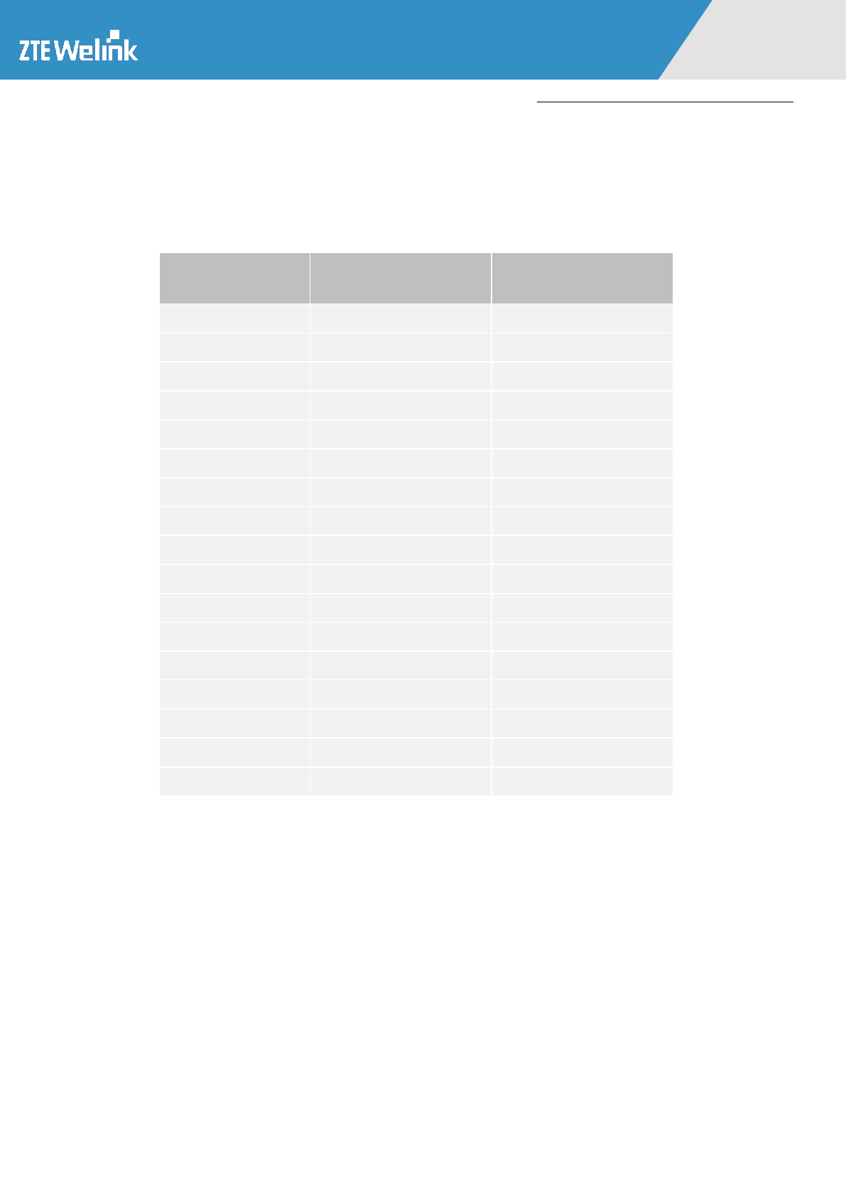
1.3 Supported & Reference Document List
Besides this hardware development document, ZTEWelink also provides the software development
guide. Table 1-1 is the list of supported documents.
Table 1–1 List for Supported& Related Documents
NUM
Document Name
1
ZTEWelink Software Development Guide of LTE Module Products-V2.3.pdf
2
ZTEWelink ZM8620_V2 Module Specification.pdf
3
AT Command reference guide for ZTEWelink LTE Module.pdf
4
3GPP LTE 36.101 protocol (Evolved Universal Terrestrial Radio Access
(E-UTRA); User Equipment (UE) radio transmission and reception)
Hardware Development Guide of Module Product
All Rights reserved, No Spreading abroad without Permission of ZTEWelink 2
错误!未找到
用源。
ZM8620_V2
5
3GPP TS 34.121 protocol
1.4 Abbreviations
Table 1-2 is a list of the relevant abbreviations, and interpretations in Chinese and English involved in
the whole document.
Table 1–2 Abbreviation List
Abbreviations
English full name
BER
Bit Error Rate
DCE
Data circuit-terminating equipment
DL
Downlink
DTE
Data terminal equipment
DTR
Data terminal ready
DPCH
Dedicated Physical Channel
DPCH_Ec
Average energy per PN chip for DPCH. DPCH
EMC
Electromagnetic compatibility
ESD
Electro-Static discharge
FDD
Frequency Division Duplexing
GPRS
General Packet Radio Service
GSM
Global Standard for Mobile Communications
I/O
Input/output
LED
Light Emitting Diode
PCB
Printed Circuit Board
SIM
Subscriber Identification Module
SMS
Short Message Service
SPI
Serial Peripheral Interface
UART
Universal asynchronous receiver-transmitter
UMTS
Universal Mobile Telecommunication System
USB
Universal Serial Bus
WCDMA
Wideband Code Division Multi Access
Hardware Development Guide of Module Product
All Rights reserved, No Spreading abroad without Permission of ZTEWelink 3
错误!未找到
用源。
ZM8620_V2
2 Product Overview
ZM8620_V2 is a multimode wireless communication module with mini-PCIE express interface, which
can be applied in but not limited to equipment such as Tablet, Vehicle Mounted Terminals, CPE and
electronic consumer products, and provides equipment with high-speed data access service in mobile
environment (LTE FDD, UTMS and GSM network).
ZM8620_V2contains two variants ZM8620_V2EUD and ZM8620_V2LAT. Customer can choose the
dedicated type based on the wireless network configuration. The following table shows the entire radio
band configuration of ZM8620_V2series.
Table 2–1 The bands informaiton of ZM8620_V2 module
BAND
ZM8620_V2EUD
ZM8620_V2LAT
FDD-LTE
BAND 1
√
√
BAND 2
--
√
BAND 3
√
--
BAND 4
--
√
BAND 5
--
√
BAND 7
√
√
BAND 8
√
√
BAND12
--
√
BAND 20
√
--
TD-LTE
BAND 38
--
√
BAND 40
√
--
UMTS
BAND 1
√
√
BAND 2
√
√
BAND 4
--
√
BAND 5
√
√
BAND 8
√
√
GSM
Quadband
√
√
NOTE:
In the Table 2-1 ―√‖ means theband is supported by module ZM8620_V2, while ―--‖ means not
supported
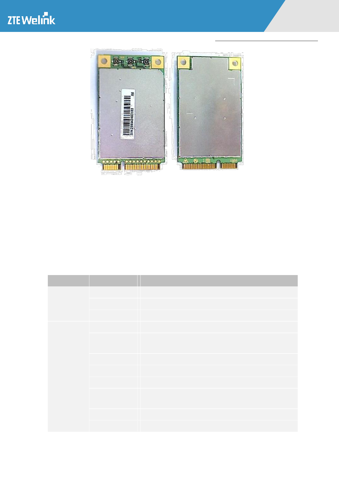
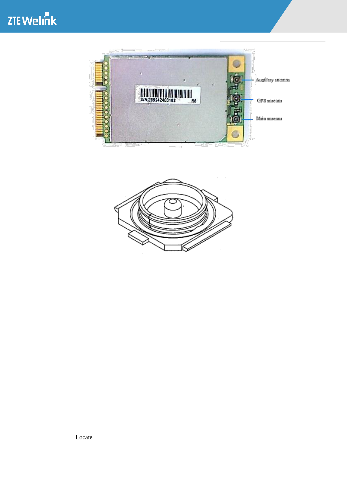
The Figure 2-1 below shows the product material object picture.
Hardware Development Guide of Module Product
All Rights reserved, No Spreading abroad without Permission of ZTEWelink 4
错误!未找到
用源。
ZM8620_V2
Figure 2–1 Product Material Object Picture
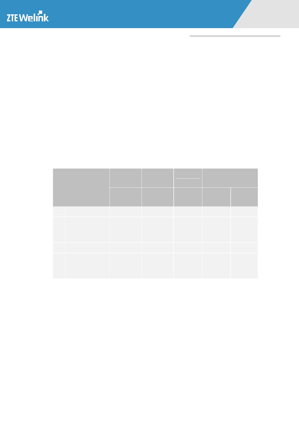
2.1 Product Technical Parameter
The major features of ZM8620_V2 can be described from the aspects of mechanic feature, base band,
radio frequency, technical standard and environment feature. Table 2-2 is a list of the major technical
parameters and features supported by ZM8620_V2.
Table 2–2 Overview of Major Technical Parameters
Item
Feature
Specifications
Mechanic
Specifications
Dimensions
51mm x 30mm x 4.9mm
Weight
About 11g
Form Factor
Mini-PCIE package(52Pin)
Baseband
(U)SIM/SIM
3V SIM card and 1.8V SIM card
Memory(SDRAM/
NAND)
128MByte & 256MByte
MICRO SD Card
No memory card support
USB Version
USB 2.0 HIGH SPEED
UART Interface
Yes
Reset/Power_on/Po
wer_off interface
Yes
SPI Interface
Yes
Maximum power
TBD

Hardware Development Guide of Module Product
All Rights reserved, No Spreading abroad without Permission of ZTEWelink 5
错误!未找到
用源。
ZM8620_V2
Item
Feature
Specifications
consumption
Power supply
Typical is 3.3V, the range is 3.

Hardware Development Guide of Module Product
All Rights reserved, No Spreading abroad without Permission of ZTEWelink 6
错误!未找到
用源。
ZM8620_V2
Item
Feature
Specifications
Equalization
Yes
Main Antenna
Provide external main Antenna Interface of RF connector mode
GPS Antenna
Provide external GPS Antenna Interface of RF connector mode
Receive Diversity
Antenna
Provide external Diversity Antenna Interface of RF connector
mode
Technical
Standard
LTE TDD
DL 50Mbps / UL 25Mbps (10MHz)
GSM/EDGE/WCD
MA
GSM CS: UL 9.6kbps/DL 9.6kbps
GPRS: Multi-slot Class 10
EDGE: Multi-slot Class 12
WCDMA CS: UL 64kbps/DL 64kbps
WCDMA PS: UL 384kbps/DL 384kbps
HSDPA/HSUPA/
HSPA+/
DC-HSPA+
HSDPA Rel 6: DL 14.4Mb/s
HSUPA Rel 6: UL 5.76Mb/s
HSPA+ Rel 7: DL 28/UL 5.76Mb/s
DC-HSPA+ Rel 8: DL 42/UL 5.76 Mb/s
CDMA 1xEV-DO
N/A
LTE-FDD
DL 100Mbps / UL 50Mbps (Category 3)
3GPP Release
R99, R5, R6, R7, R8(HSPA+),R9(FDD)
OS
Windows XP/Vista/7/8, Android, Linux, WinCE
GPRS Class
Class A
Environment
Operating
Temperature
-10 to 60 °C
Storage
Temperature
-40 to 85 °C
Humidity
5%~ 95%
Application
DATA
RAS
Yes
ECM
Yes
NDIS
Yes
SMS
Yes
MMS
Yes, not support embedded MMS stack
STK
No
TCP/IP
No
USSD
Yes (Phase I &Phase II)
Phonebook
Yes
Hardware Development Guide of Module Product
All Rights reserved, No Spreading abroad without Permission of ZTEWelink 7
错误!未找到
用源。
ZM8620_V2
Item
Feature
Specifications
NETWORK
LOCK
No
BAND LOCK
Yes
SIM Reader
Yes
Firmware Update
Yes
GPS/AGPS
Yes
2.2 Function Overview
2.2.1 Baseband Function
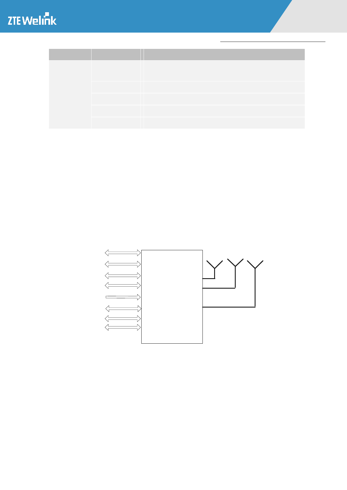
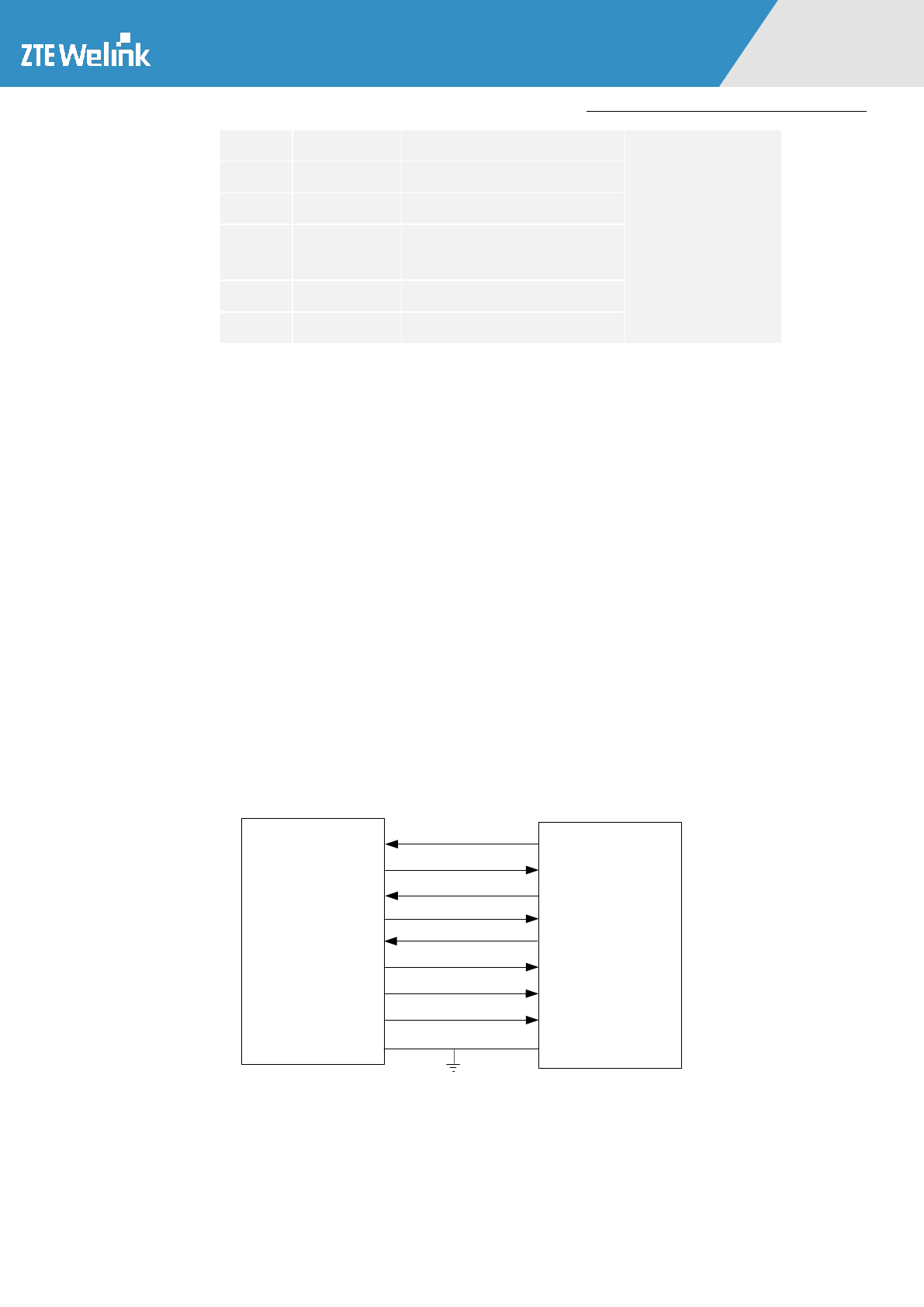
When connect the module product ZM8620_V2 to the system board, there are several main signal
groups as follows: USB signal, SIM card signal, UART signal, GPIO signal, SPI signal, power on and
resetting signal, wakeup signal, power supply and ground. At the same time, ZM8620_V2 has the main
antenna interface, diversity antenna interface, and GPS antenna interface.
Main
Antenna
USB
SIM card
POWER
GND
GPIO
UART
WAKE#&PERST#&W
_DISABLE Signals
GPS
Antenna
ZM8620_V2
PCIE LTE wireless
Internet access
module
Diversity
Antenna
SPI
Figure 2–2 System Connection Diagram
2.2.2 Radio Frequency Function
The radio frequency function of ZM8620_V2 can be viewed from the aspect of over-the-air wireless
bearer network, frequency band, whether receive diversity feature is supported.
(a) Support LTE FDD, LTE TDD, UMTS;
Hardware Development Guide of Module Product
All Rights reserved, No Spreading abroad without Permission of ZTEWelink 8
错误!未找到
用源。
ZM8620_V2
(b) Support GSM 850/900/1800/1900 MHz;
(c) Support the diversity receives;
The operating frequencies of module ZM8620_V2 are shown as Table 2-3.
Table 2–3 Product Operating Frequency Band
Operating Frequency
Band
Uplink Frequency Band
(Uplink)
Downlink Frequency Band
(Downlink)
UMTS850
824 MHz — 849 MHz
869 MHz — 894 MHz
UMTS900
880 MHz — 915 MHz
925 MHz — 960 MHz
UMTS1700
1710 MHz — 1755MHz
2110 MHz — 2155MHz
UMTS1900
1850 MHz — 1910 MHz
1930 MHz — 1990 MHz
UMTS2100
1920 MHz — 1980 MHz
2110 MHz — 2170 MHz
GSM1900
1850 MHz — 1910 MHz
1930 MHz — 1990 MHz
GSM850
824 MHz — 849 MHz
869 MHz — 894 MHz
GSM900
890 MHz — 915MHz
935 MHz — 960MHz
GSM1800
1710 MHz — 1785MHz
1805 MHz — 1880MHz
LTE-FDD Band17
788 MHz — 798 MHz
734 MHz — 746 MHz
LTE-FDD Band5
824 MHz — 849MHz
869 MHz — 894 MHz
LTE-FDD Band8
880 MHz — 915 MHz
925 MHz — 960 MHz
LTE-FDD Band4
1710 MHz — 1755MHz
2110 MHz — 2155 MHz
LTE-FDD Band2
1850 MHz — 1910MHz
1930 MHz — 1990MHz
LTE-FDD Band1
1920 MHz — 1980 MHz
2110 MHz — 2170 MHz
LTE-FDD Band7
2500 MHz — 2570MHz
2620 MHz — 2690MHz
LTE-TDD Band38
2570 MHz — 2620MHz
2570 MHz — 2620MHz
Hardware Development Guide of Module Product
All Rights reserved, No Spreading abroad without Permission of ZTEWelink 9
错误!未找到
用源。
ZM8620_V2
3 Mechanic Feature
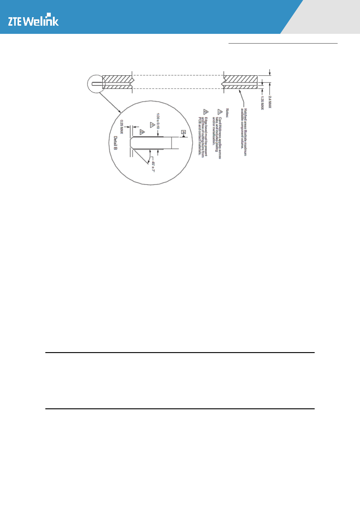
3.1 Dimensions and Interface
This product adopts the standard PCI Express Mini Card interface type, and the contour size is designed
according to F1 type. Figure 3-1 illustrates the dimensions and slot compatibility of PCI Express Mini
Card.
Users of this module can refer to the document named PCI Express Mini Card Electromechanical
Specification Revision 1.2, October 26 2007 for the detail of PCIE interface.
Table 3–1 PCI Express Mini Card
Card Type
Full-Mini-
Only Socket
Half-Mini-
Only Socket
Dual-Use
Socket
Dual Head-to-Head
Socket
Connector
A
Connector
A
Connector
A
Connector
A
Connector
B
F1
Full-Mini
Yes
No
No
No
No
F2
Full-Mini with
bottom-side keep
outs
Yes
No
Yes
Yes
No
F3
Half-Mini
No
Yes
Yes
Yes
No
F4
Half-Mini with
bottom-side keep
outs
No
Yes
Yes
Yes
Yes
Hardware Development Guide of Module Product
All Rights reserved, No Spreading abroad without Permission of ZTEWelink 10
错误!未找到
用源。
ZM8620_V2
(a)
(b)
Hardware Development Guide of Module Product
All Rights reserved, No Spreading abroad without Permission of ZTEWelink 11
错误!未找到
用源。
ZM8620_V2
(c)
Figure 3–1 PCI Express Mini Card Dimensions Type and Slot Compatibility
Figure (a) is TOP surface dimensions; Figure (b) is BOTTOM surface dimensions; Figure (c) is
thickness information.
3.2 Antenna Interface
This product has three radio frequency antenna interfaces: One is the main antenna interface (there is the
―MAIN‖ flag on the PCB), one is a diversity receiving antenna (diversity optional) interface (there is
―AUX‖ flag on the PCB), and one is GPS antenna, as shown in Figure 3-2. The radio frequency bases
adopted by the antenna interface of ZM8620_V2 module are all U.FL-R-SMT-1(80)(HRS)/
ECT818000071(ECT) at present as shown in Figure 3-3.
NOTE:
The radio frequency bases adopted by the antenna interface of ZM8620_V2 module is
U.FL-R-SMT-1(80)(HRS)/ECT818000071(ECT) at present instead of adopting 20429-001E MHF-A13
of I-PEX by ZM8620 before.
Hardware Development Guide of Module Product
All Rights reserved, No Spreading abroad without Permission of ZTEWelink 12
错误!未找到
用源。
ZM8620_V2
Figure 3–2 Antenna Interface Flag Diagram (with Diversity)
Figure 3–3 Radio Frequency Interface Test Base
This product antenna is placed on the side of the system board. If this product is embedded in a notebook,
place it on the top of the LCD screen.
3.3 Thermal Design
The thermal design of this product strictly complies with the specification [PCI Express Mini Card
Electromechanical Specification Revision 1.2, October 26, 2007], and distributes the heat source evenly,
and has excellent heat dissipating design. As the maximum power consumption of the overall system is
very high when transmitting, if it is impossible to ensure the temperature of ZM8620_V2 less than 60°C,
the rise of the overall system temperature will lead to the performance degradation of ZM8620_V2, or
even not operate normally. In order to ensure product performance, safety and stability, the following
proposals are provided for the main board design:
(a) the module far away from the switch power and high-speed signal cable as much as

Hardware Development Guide of Module Product
All Rights reserved, No Spreading abroad without Permission of ZTEWelink 13
错误!未找到
用源。
ZM8620_V2
possible. Well protect the wiring of the interference sources.
(b)
located close the interference sources.
(c) the module close to devices with large heat dissipation, such as CPU, south
bridge, etc. The high temperature will affect the RF performance.

Hardware Development Guide of Module Product
All Rights reserved, No Spreading abroad without Permission of ZTEWelink 14
错误!未找到
用源。
ZM8620_V2
4 Pin Description
4.1 Dimensions and Interface
4.1.1 Definition of PIN I/O Parameters
The definition of the module‘s I/O parameter is as shown in Table 4-1.
Table 4–1 PIN Parameters
PIN Attribute
Description
AI
Analog signal input
AO
Analog signal output
B
bidirectional digital with CMOS
input
DI
Digital signal input
DO
Digital signal output
Z
High-resistance output
P1
PIN group 1, the power supply
voltage is VDD_P1
P2
PIN group 2, the power supply
voltage is VDD_P2
PU
PIN internal pull-up
PD
PIN internal pull-down
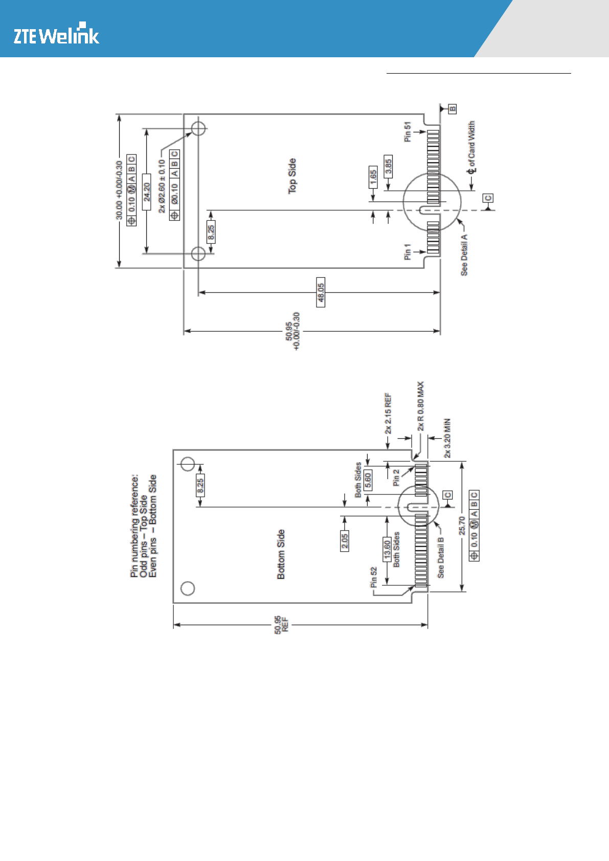
4.1.2 PIN Configuration Diagram
The PIN sequence of interfaces on the module is following the mini-PCIE interface and defined as
shown in Figure 4-2.
Hardware Development Guide of Module Product
All Rights reserved, No Spreading abroad without Permission of ZTEWelink 15
错误!未找到
用源。
ZM8620_V2
Figure 4–1 PIN Distribution Diagram
12
3
5
7
9
11
13
15
17
19
21
23
25
27
29
31
33
35
37
39
41
43
45
49
51
4
6
8
10
12
14
16
18
20
22
24
26
28
30
32
34
36
38
40
42
44
46
48
50
52
VDD_3V3
VREG_UIM
UIM_ DATA
UIM_ CLK
UIM_ RST
UART1_DSR
W
_DISABLE_N
PERST#
VDD_3V3
USB_ DM
USB_ DP
VDD_3V3
VDD_3V3 LED_ PWR
VDD_3V3
47
GND
SPI_CS
GND
GND
GPIO
NC
GND
GND
NC
SLIC_INT
SLIC_RESET
GND
WAKE #
SPI_SDI
SPI_SDO
SPI_CLK
GND
GND
GND
GND
GND
GND
GND
UART1_RX
UART1_RI
GPIO_79
UART1_CTS
UART1_RFR
UART1_DTR
GND
RESERVED
RESERVED
RESERVED
RESERVED
COEX1
COEX2
CLKREQ*
GND[1]
REFCLK-
REFCLK+
GND[2]
RESERVED5_UIM_C8
RESERVED4_UIM_C4
GND[4]
PERN0
PERP0
GND[6]
GND[7]
PETN0
PETP0
GND[9]
GND[10]
3V3VAUX[2]
3V3VAUX[3]
GND[12]
RESERVED3
RESERVED2
RESERVED0
RESERVED1
3V3VAUX[0]
GND[0]
1V5[0]
UIM_PWR
UIM_DATA
UIM_CLK
UIM_RESET
UIM_VPP
W_DISABLE*
PERST*
3V3VAUX[1]
GND[5]
1V5[1]
SMB_CLK
SMB_DATA
GND[8]
USB_D+
LED_WWAN*
LED_WLAN*
LED_WPAN*
1V5[2]
GND[13]
3V3VAUX[4]
ZM8620_V2
USB_D-
GND[11]
GND[3]
UART1_DCD
UART1_TX
NC
Figure 4–2 PIN Configuration Diagram
4.1.3 PIN Description
Table 4–2 PIN Interface Definition

Hardware Development Guide of Module Product
All Rights reserved, No Spreading abroad without Permission of ZTEWelink 16
错误!未找到
用源。
ZM8620_V2
Pin
Standard PIN
ZM8620_V2 PIN
Description
I/O
Remark
1
WAKE#
WAKE#
Wake up the system host
DO
--
2
3.3Vaux
VDD_3V3
3.3V supply
DI
3.1V-3.6V,The
typical value is
3.3V
3
COEX1
SPI_SDI
SPI data signal
DI
3.3V
4
GND
GND
Ground
--
Ground pin
5
COEX2
SPI_SDO
SPI data signal
DO
3.3V
6
1.5V
SPI_CS
SPI segment signal
DO
3.3V
7
CLKREQ#
SPI_CLK
SPI synchronization clock
--
3.3V
8
UIM_PWR
VREG_UIM
USIM card power supply
DO
2.85V/1.8V for
SIM card
9
GND
GND
Ground
--
Ground pin
10
UIM_DATA
UIM_DATA
USIM card data signal
DI/DO
2.85V/1.8V.this
signal requires a
pull-up resistor
on the host board
11
REFCLK-
UART1_RX
UART port receive data
DI
3.3V
12
UIM_CLK
UIM_CLK
USIM card clock signal
DO
2.85V/1.8V
13
REFCLK+
UART1_TX
UART port transmit data
DO
3.3V
14
UIM_RESET
UIM_RST
USIM card reset signal
DO
2.85V/1.8V
15
GND
GND
Ground
--
Ground pin
16
UIM_VPP
UATR1_DSR
Data is ready
DO
1.8V
17
Reserved(UIM_C8)
UART1_RI
Ringtone indicator
DO
1.8V
18
GND
GND
Ground
--
Ground pin
19
Reserved(UIM_C4)
GPIO_79
The standby and wakeup of
module
--
--
20
W_DISABLE#
W_DISABLE_N
Active low signal. This
signal is used by the system
to disable radio operation on
add-in cards that implement
radio frequency applications.
DI
Active low
21
GND
GND
Ground
--
Ground pin
22
PERST#
PERST#
Module resetting
DI
1.8V
23
PERn0
UART1_CTS
UART port, clear to send
DI
1.8V
24
+3.3Vaux
VDD_3V3
3.3V supply
DI
3.1V-3.6V,The
typical value is
3.3V
25
PERp0
UART1_RFR
UART port, preparing to
receive
DO
1.8V
26
GND
GND
Ground
--
Ground pin
27
GND
GND
Ground
--
Ground pin

Hardware Development Guide of Module Product
All Rights reserved, No Spreading abroad without Permission of ZTEWelink 17
错误!未找到
用源。
ZM8620_V2
Pin
Standard PIN
ZM8620_V2 PIN
Description
I/O
Remark
28
+1.5V
GPIO
General Purpose
Input/Output
DI/DO
1.8V
29
GND
GND
Ground
--
Ground pin
30
SMB_CLK
NC
--
--
--
31
PETn0
UART1_DTR
UART1 data terminal ready
DI
1.8V
32
SMB_DATA
NC
--
--
--
33
PETp0
UART1_DCD
UART1 carrier wave
detection
DO
1.8V
34
GND
GND
Ground
--
Ground pin
35
GND
GND
Ground
--
Ground pin
36
USB_D-
USB_DM
USB differential signal,
minus side
DI/DO
--
37
GND
GND
Ground
--
Ground pin
38
USB_D+
USB_DP
USB differential signal,
positive side
DI/DO
--
39
+3.3Vaux
VDD_3V3
3.3V supply
DI
3.1V-3.6V,The
typical value is
3.3V
40
GND
GND
Ground
--
Ground pin
41
+3.3Vaux
VDD_3V3
3.3V supply
DI
3.1V-3.6V,The
typical value is
3.3V
42
LED_WWAN#
LED_PWR
Open drain,active low
signals. This signal is used
to provide status indicator
DO
--
43
GND
GND
Ground
--
Ground pin
44
LED_WLAN#
NC
--
--
--
45
Reserved
Reserved
--
--
--
46
LED_WPAN#
SLIC_INT
exclusive use for routing
adaptation
DO
--
47
Reserved
Reserved
--
--
--
48
+1.5V
SLIC_RESET
exclusive use for routing
adaptation
DO
--
49
Reserved
Reserved
--
--
--
50
GND
GND
Ground
Ground pin
51
Reserved
Reserved
--
--
--
52
+3.3Vaux
VDD_3V3
3.3V supply
DI
3.1V-3.6V,The
typical value is
3.3V

Hardware Development Guide of Module Product
All Rights reserved, No Spreading abroad without Permission of ZTEWelink 18
错误!未找到
用源。
ZM8620_V2
NOTE:
The voltage design of external circuit interfaces should match that of the ZM8620_V2 PINs.
In the Table 4-2, the Power supply of ZM8620_V2 has been updated between 3.1V-3.6V, and the typical
value is 3.3V at present. While in ZM8620 module, the Power supply is 3.4-4.2V, and typical is 3.8V
before.
In ZM8620_V2, the signal of pin 6,11,13,16,17,23,25,28,30~33,44,46.48 is different from that of
module ZM8620.
4.2 Feature of Interface Power Level
4.2.1 Power Level of IO Interface
Table 4–3 Power Level Range of Digital Signal
Signal
Description
Min
Max
Units
VIH
High level of input voltage
0.65*VDD_PX
VDD_PX+0.3
V
VIL
Low level of input voltage
-0.3
0.35*
VDD_PX
V
VOH
High level of output
voltage
VDD_PX-0.45
VDD_PX
V
VOL
Low level of output
voltage
0
0.45
V
NOTE:
1. The high/low PWL of input voltage should comply with the range in the table.
2. The high/low PWL of external interface signal should match the interface PWL of ZM8620_V2.
3. VDD_PX indicates the typical voltage of each Pin specified in Table 4-2.
Hardware Development Guide of Module Product
All Rights reserved, No Spreading abroad without Permission of ZTEWelink 19
错误!未找到
用源。
ZM8620_V2
4.3 Power Interface
4.3.1 Description of Power PINs
Power VCC (PIN No: 2, 24, 39, 41, 52). This is the positive signal of 3.3V power supply.
GND signal (PIN No: 4, 9, 15, 18, 21, 26, 27, 29, 34, 35, 37, 40, 43, 50). This is the power ground and
signal ground of the module, which needs to be connected to the ground on the system board. If the
GND signal is not connected completely, the performance of the module will be affected.
4.3.2 Requirement of Power Supply
The power supply is recommended to be within the range of 3.1~3.6V. If the network is in poor situation,
the antenna will transmit at the maximum power, and the transient maximum peak current less than 2G
mode can reach as high as 1.8A. So the power supply capacity for peak current needs to be above 2.5A,
and the average peak current needs to be above 0.9A.
4.4 (U)SIM Card Interface
4.4.1 Description of PINs
ZM8620_V2 module baseband processor integrates the (U)SIM card interface. The signals on SIM card
interface is as shown in Figure 4-3.
Figure 4–3 (U)SIM Card Signal Connection Circuit
VREG_UIM
VREG_UIM

Hardware Development Guide of Module Product
All Rights reserved, No Spreading abroad without Permission of ZTEWelink 20
错误!未找到
用源。
ZM8620_V2
NOTE:
The PCB wiring of UIM card should be laid closely around the module as possible as you can, and the
ESD component should be put near the UIM card socket by the customer.
Table 4–4 Definition & Description of (U) SIM Card Signal Group
PIN
Signal Name
Signal Description
8
VREG_UIM
USIM card power, output from the module
10
UIM_DATA
USIM card DATA signal, two-way signal
12
UIM_CLK
USIM card clock signal, output from the module
14
UIM_RST
USIM card reset signal, output from the module
4.4.2 Electric Feature
The signals of (U)SIM card signal group are described in Table 4-4. As the USIM card console is placed
on the system board side, be sure to add the ESD protection during the design.
To comply with the requirements of 3GPP TS 51.010-1 and EMC authentication, it is recommended to
place (U)SIM card console close to the (U)SIM card interface, to prevent the wiring from being too long,
which might seriously distort the waveform and thus affect the signal integrity. It is recommended to
make the grounding protection for UIM_CLK and UIM_DATA signal wiring.
Cascade one 0.1uF and 33pF capacitor between VREG_UIM and GND, and cascade a 33pF bypass
capacitor between UIM_CLK, UIM_RST and GND, to filter out the interference by RF signals. It is
recommended to cascade a 20ohm resistance on UIM_DATA signal. And UIM_DATA must be pulled up
via a 20K ohm resistance to VREG_UIM.
4.5 USB2.0 Interface
4.5.1 Description of PINs
ZM8620_V2 has the high-speed USB2.0 interface,. USB is connected to the system board side via the
PCI-E interface, to communicate with the processor on the system board side. Its PINs are PIN36
(USB_DM), PIN38 (USB_DP). The USB interface can be mapped to difference ports, such as
Diagnostics port to capture the log, AT port is used to complete AT command interaction with the AP
side.
Hardware Development Guide of Module Product
All Rights reserved, No Spreading abroad without Permission of ZTEWelink 21
错误!未找到
用源。
ZM8620_V2
4.5.2 Electric Feature
The USB interface of Module complies with the USB2.0 specifications and the electrical characteristics.
During the PCB wiring, the wires must be parallel, the distance should be as short as possible and as far
away as possible from the antenna, and it‘s enveloped by the ground wires to avoid strong interference
sources. USB_DP and USB_DM should be wired strictly in the differential mode, and the length
difference of the two signals is within 1mm.
NOTE:
The differential resistance needs to be controlled within 90Ω, and the difference cannot exceed 5%.
It is recommended to cascade the high-speed common-mode rejection filter on the USB differential
traces. If some of the trace is exposed, it is recommended to add the ESD protection device, and the
junction capacitor of the ESD protection device should better be kept within 1.5pF. Large junction
capacitor will distort the waveform, and affect the bus communication.
4.6 UART Interface
The UART interface is used as MODEM port by default which is occupied by data service.
4.6.1 Description of PINs
The wireless module ZM8620_V2 supports the full UART interface with flow control function, which
complies with the RS-232 interface protocol, and supports the 8-wires serial bus interface or 2-wires
serial interface. The module can perform the serial communication and AT instruction interaction with
external.
This UART port supports the programmable data width, programmable data stop bit and programmable
parity check, and has an independent TX and RX FIFOs (512 bytes for each). For the normal UART
application (non-Bluetooth), the maximum baud rate is 230400bps, and the default baud rate is
115200bps. The PINs are defined as shown in Table 4-5.
Table 4–5 Definition of UART Signal
PIN
Signal Name
Description
Level
11
UART1_RX
UART port RX receive data
Power level is 3.3V.
13
UART1_TX
UART port TX transmit data
Power level is 3.3V.
Hardware Development Guide of Module Product
All Rights reserved, No Spreading abroad without Permission of ZTEWelink 22
错误!未找到
用源。
ZM8620_V2
16
UART1_DSR
Data is ready
Power level is 1.8V.
17
UART1_RI
Ringtone indicator
23
UART1_CTS
UART port CTS clear to send
25
UART1_RFR
UART port RFR preparing to
receive
31
UART1_DTR
DTE is ready
33
UART1_DCD
Carrier detection
4.6.2 Electric Feature
During the software interconnection process, there is a method of capturing logs, and it is recommended
that this interface be kept during the design and the testing point be reserved. If the module is used
together with the application processor, and the PWL of it matches with the power level of the module,
the connection mode is as shown in Figure 4-4. The 4-wires or 2-wires mode can also be used for
connection. If it does not match the PWL of AP interface, it is recommended to add the PWL conversion
circuit. Otherwise, it might cause unstable com ports because the level is not matched or cause damage
to the module because it is at high level for long time.
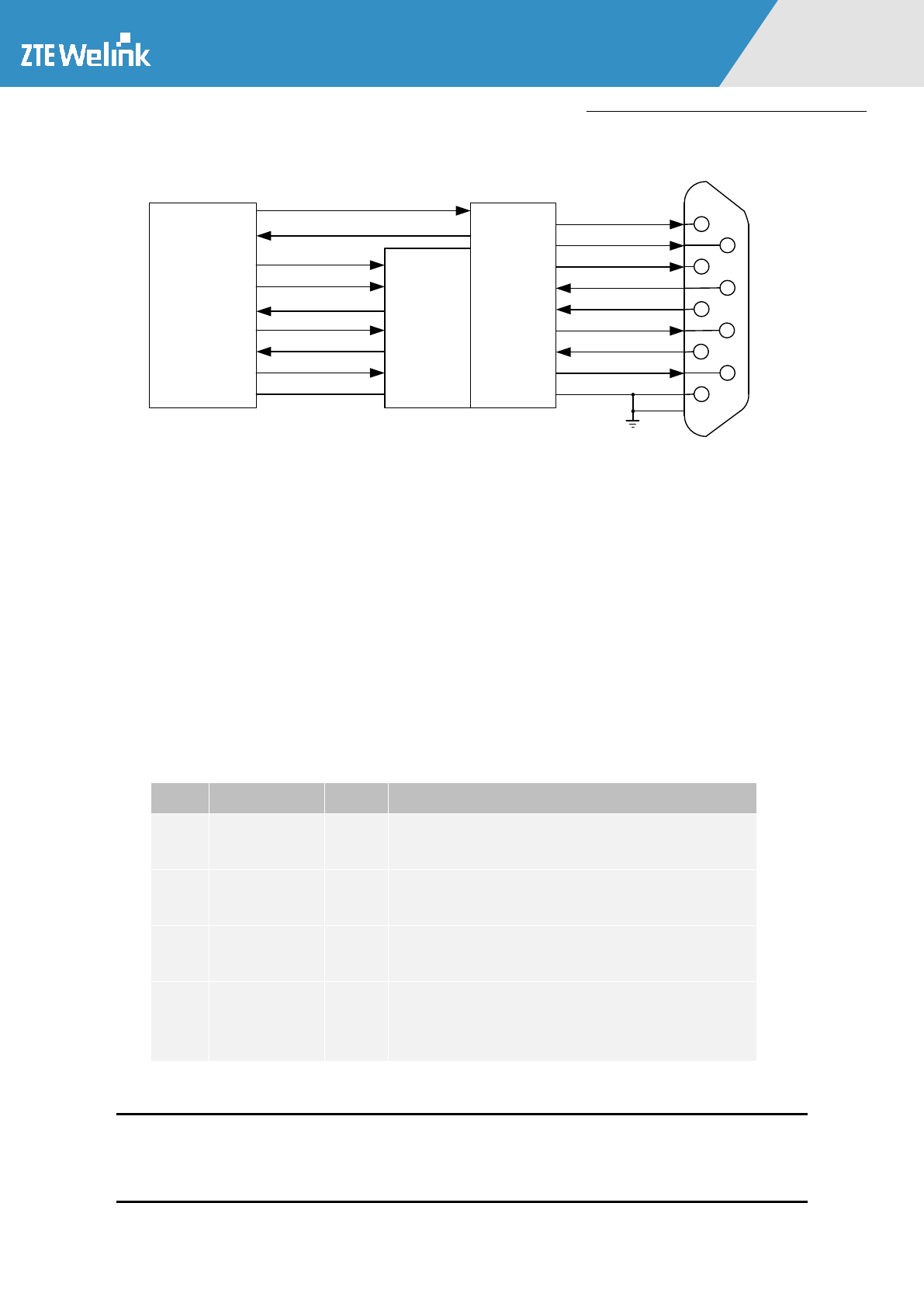
The connection of ZM8620_V2 UART port and standard RS-232-C interface can be through the chip
like class 232. The design involves the transformation of TTL level and EIA level. We recommend to
use the chip of NLSX5014MUTAG. If using the 2-byte serial bus interface, MAX3232 is recommended,
and if using the 8-byte serial bus interface, SP3238 or MAX3238 is recommended. The connection mode
is as shown in Figure 4-5.
ZM8620_V2 AP
RXD
RXDTXD
TXD
CTS
RFR CTS
RFR
DTR
DSRDSR
DTR
DCD
RI RI
DCD
GND GND
Figure 4–4 Module Serial Port & AP Application Processor
Hardware Development Guide of Module Product
All Rights reserved, No Spreading abroad without Permission of ZTEWelink 23
错误!未找到
用源。
ZM8620_V2
TTL-
RS232
level
translator
SP3238
MAX3238
ZM8620_
V2
module
1.8V
-TTL
level
translator
NLSX5014MUTAG
UART_DCD
UART_DSR
UART_CTS
UART_RFR
UART_DTR
UART_RI
GND
RS232_DCD
RS232_DSR
RS232_TXD
RS232_CTS
RS232_RXD
RS232_RTS
RS232_DTR
RS232_RI
GND
1
2
3
4
5
6
7
8
9
User Board Female DB9
Note:UART_RFR is equal To UART_RTS.
The level of UART1_Rx and UART1_TX is 3.3V, the other pins of UART is
1.8V and needs the TTL level translator
UART_TXD
UART_RXD
Figure 4–5 The connection of ZM8620_V2 UART and Standard RS-232-C interface
4.7 SPI Interface
The SPI signal interface is used to control PCI voices. The SPI_CLK clock is 127.2kHz. Pin No: 3/5/6/7
are SPI control signals. Table 4-6 describes detailed definition for each signal. The system board side
needs to convert the power level of SPI_SDI (SPI control output signal cable on the system board side)
into 3.3V, to comply with the high power level VIH input requirements.
Table 4–6 Definition and Description of SPI Control Signal Group
PIN
Signal Name
I/O
Signal Description
3
SPI_SDI
I
SPI data signal, ZM8620_V2 input, input high power
level is VIH, and low power level is VIL.
5
SPI_SDO
O
SPI data signal, ZM8620_V2 output, input high power
level is VOH, and low power level is VOL.
6
SPI_CS
O
SPI chip select pin, ZM8620_V2 output, input high
power level is VOH, and low power level is VOL.
7
SPI_CLK
--
SPI synchronization clock, 100kHz, output by
ZM8620_V2, high power level is VOH, and low power
level is VOL.
NOTE:
VIH, VIL, VOH, and VOL comply with the power I/O interface power level requirements in 4.2.1.
Hardware Development Guide of Module Product
All Rights reserved, No Spreading abroad without Permission of ZTEWelink 24
错误!未找到
用源。
ZM8620_V2
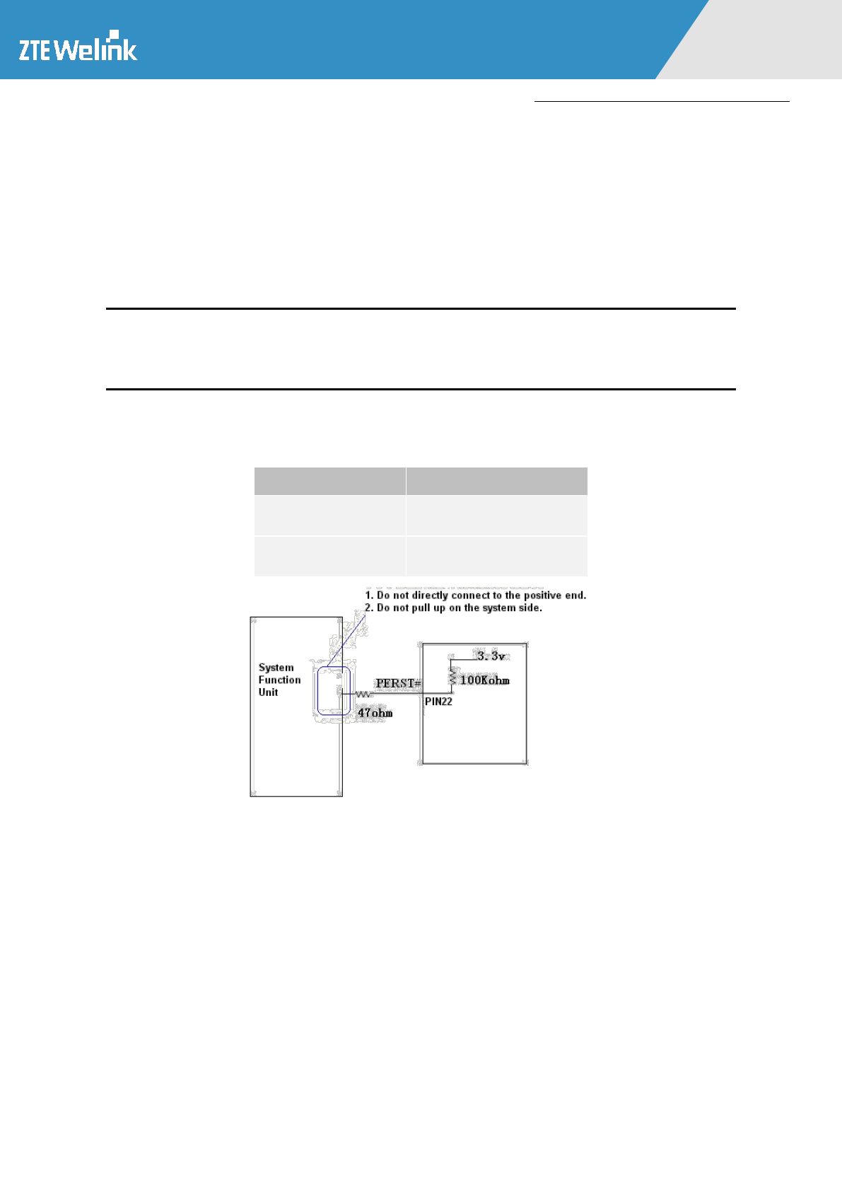
4.8 Reset Signal PERST#
The PERST# signal (PIN No: 22) is the system reset signal of ZM8620_V2, active low. Table 4-7
illustrates its control logic. It shows that pull down the reset key (PERST#) to 100ms will reset the
module.
NOTE:
Do not directly connect this signal to the positive end of power supply.
Table 4–7 Definition and Description of PERST# Signal
PERST#
ZM8620_V2 Status
‗1‘
ZM8620_V2 is in the
normal working status.
‗0‘ and ≥100ms
RF is in the OFF mode,
ZM8620_V2 is reset.
Figure 4–6 Reference Circuit Design of PERST# Signal
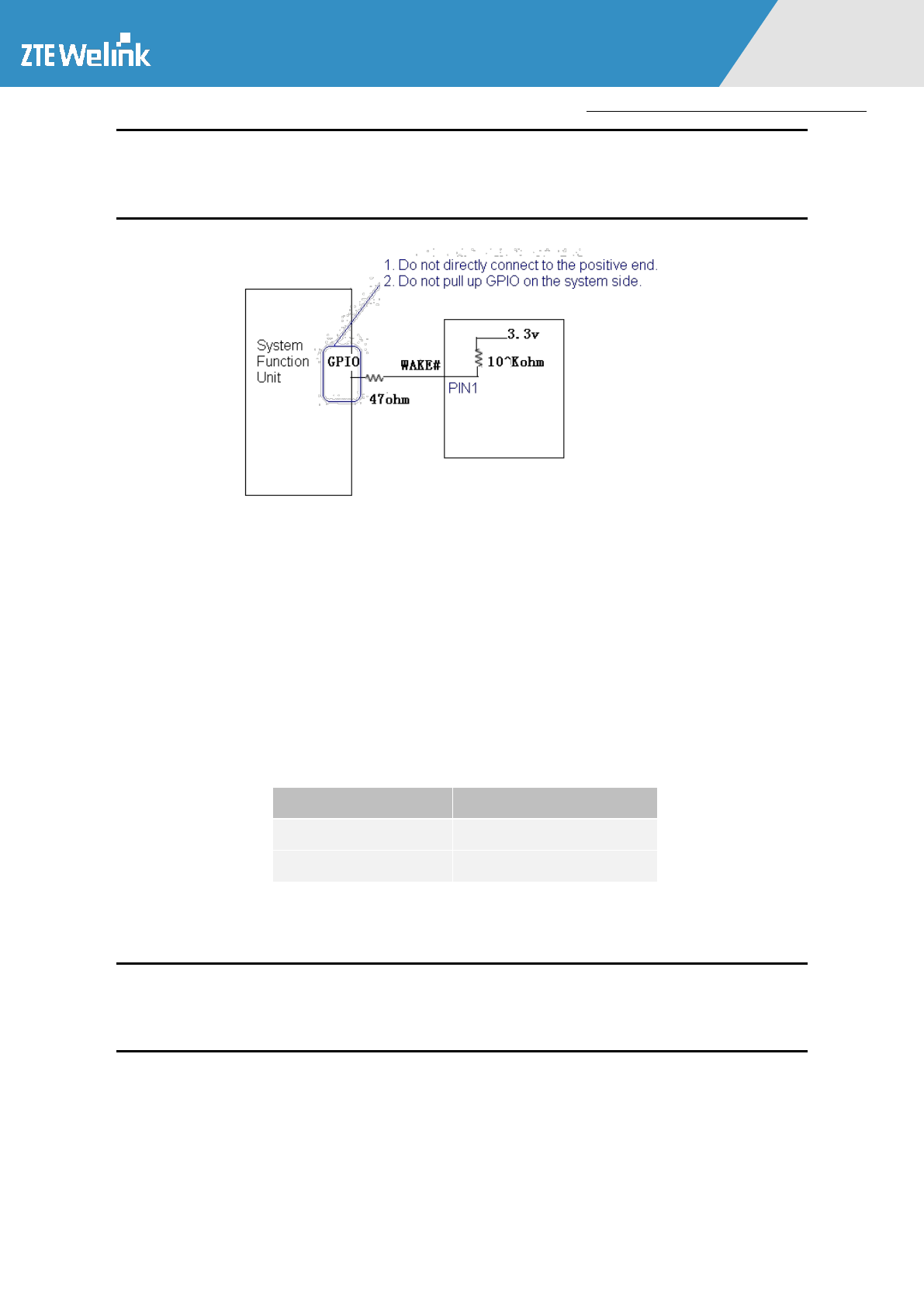
4.9 WAKE# Signal
Figure 4-7 illustrates the reference connection circuit of WAKE# signal. The WAKE# signal (PIN No.: 1)
is an output signal, active low level or low fall edge. This signal is a reserved signal for ZM8620_V2 to
wake up the system host. ZM8620_V2 pulls up the power level to VDD_3V3 internally by the 10Kohm
resistance. It is recommended to connect the 47ohm resistance to the GPIO PIN on the main chip (If this
GPIO PIN is on the system side, it can wake up the host).
ZM8620_V2
Hardware Development Guide of Module Product
All Rights reserved, No Spreading abroad without Permission of ZTEWelink 25
错误!未找到
用源。
ZM8620_V2
NOTE:
Do not directly connect this signal to the positive end of power supply.
Figure 4–7 Reference Connection Circuit of WAKE# Signal
4.10 W_DISABLE_N Signal
The W_DISABLE_N signal (PIN No: 20) is the input signal of ZM8620_V2, active low. Table 4-8
describes its control logic.
Table 4–8 Definition and Description of W_DISABLE_N Signal
W_DISABLE_N
ZM8620_V2 Status
‗1‘
RF is enabled.
‗0‘
RF is disabled.
The W_DISABLE_N signal is pulled up by the 150Kohm resistance to 3.3V inside ZM8620_V2, so the
system side does not pull up this circuit any more.
NOTE:
Do not directly connect this signal to the positive end of power supply.
Figure 4-8 illustrates the reference circuit design of W_DISABLE_N signal.
ZM8620_V2

Hardware Development Guide of Module Product
All Rights reserved, No Spreading abroad without Permission of ZTEWelink 26
错误!未找到
用源。
ZM8620_V2
Figure 4–8 Reference Circuit Design of W_DISABLE_N Signal
4.11 Recommended Upgrade Methods
It‘s recommended to use the one-click software upgrade tool to upgrade through the USB port provided
by ZTEWelink in the Windows system. If the customers want to upgrade the module in other operation
systems, ZTEWelink provides the corresponding reliable tools too.
ZM8620_V2
Hardware Development Guide of Module Product
All Rights reserved, No Spreading abroad without Permission of ZTEWelink 27
错误!未找到
用源。
ZM8620_V2
5 Electric Feature
5.1 Power Feature
5.1.1 Power Supply
The input voltage range of the module is DC 3.1V~3.6V, and the typical value is 3.3V, as shown in Table
5-1.
Table 5–1 Input Voltages
Parameter
Min
Typical
Max
Input voltage
3.1V
3.3V
3.6V
5.1.2 Working Current
The working current range of the module is as shown in Table 5-2 to Table 5-4. The tables provide the
working power consumption under LTE and WCMA mode. As the power consumptions are affected by
many factors, it‘s normal that there are some differences when tested by users, and these tables can only
be viewed as one example.
Table 5–2 Averaged standby DC power consumption
Mode
Bands
Test value (mA)
Remark
HSDPA/WCDMA
UMTS bands
TBD
Sleep mode
GSM/GPRS/EDGE
GSM bands
TBD
Sleep mode
LTE
LTE bands
TBD
Sleep mode
Note: assumes USB bus is fully suspended during measurements. Under different
environments, the testing results might be slightly different. Take the actual situation as
the reference.
Table 5–3 DC power consumption in UMTS mode
Power Consumption of R99
BAND
BAND1
BAND2
BAND5
BAND8
Power Consumption
(Unit: mA)
Maximum Transmit power
(23.32dBm)
TBD
TBD
TBD
TBD
Hardware Development Guide of Module Product
All Rights reserved, No Spreading abroad without Permission of ZTEWelink 28
错误!未找到
用源。
ZM8620_V2
Power Consumption of HSDPA
Power Consumption with
HS-DPCCH (HSDPA)
Maximum Transmit power
(dBm)
22.62
22.56
22.04
22.51
Power Consumption (mA)
TBD
TBD
TBD
TBD
Power Consumption of HSUPA
Power Consumption with
HS-DPCCH (HSUPA)
Maximum Transmit power
(dBm)
22.2
21.9
21.7
21.7
Power Consumption (mA)
TBD
TBD
TBD
TBD
Power Consumption of HSPA+
Power Consumption
(Unit: mA)
Maximum Transmit power
(22.89dBm)
TBD
TBD
TBD
TBD
Table 5–4 DC power consumption in LTE mode (Unit: mA)
Test band
BAND
1
BAND
2
BAND
4
BAND
5
BAND
7
BAND
8
BAND
12
TDD
BAND38
BW 10M
band channel
300
650
2175
2450
3400
3500
5130
38200
Power
Consumpti
on
QPSK 1RB
MAX PWR
TBD
TBD
TBD
TBD
TBD
TBD
TBD
TBD
QPSK 12RB
MAX PWR
TBD
TBD
TBD
TBD
TBD
TBD
TBD
TBD
QPSK 50RB
MAX PWR
TBD
TBD
TBD
TBD
TBD
TBD
TBD
TBD
16QAM 12RG
MAX PWR
TBD
TBD
TBD
TBD
TBD
TBD
TBD
TBD
16QAM 50RG
MAX PWR
TBD
TBD
TBD
TBD
TBD
TBD
TBD
TBD
NOTE:
Under different environments and conditions (for example: under different band channel, transmit power,
power level etc.), the testing values of Table 5-3 and Table 5-4 might be slightly different. Take the
actual situation as the reference.
5.2 Power-on/Resetting Flow
Table 5–5 Power-on/Resetting Period
Hardware Development Guide of Module Product
All Rights reserved, No Spreading abroad without Permission of ZTEWelink 29
错误!未找到
用源。
ZM8620_V2
No.
Status
Average
Remark
1
Response time of
power-on and power-off
About 12s
From the time of module
power-on to port initialization
2
Searching network upon
power-on
About 15s
Depending on the actual
network situation
Note:
1. The specific power-on/power-off response time depends on the actual software versions.
The time of searching network upon power-on differs according to the network quality. The
above values are only an example.
2. By default, the module is started up upon power-on.
5.3 Resetting Flow
The failing edge of PERST# reset signal initiates a reset process. The module is reset by driving this pin
with a low pulse.
1
0
PERST# signal 100ms Resetting at
the edge of
rising
Figure 5–1 Module Reset Flow

Hardware Development Guide of Module Product
All Rights reserved, No Spreading abroad without Permission of ZTEWelink 30
错误!未找到
用源。
ZM8620_V2
6 Related Test & Testing Standard
6.1 Testing Reference
The related tests of ZM8620_V2 comply with the IEC standard, including the equipment running under
high/low temperature, storage under high/low temperature, temperature shock and EMC. Table 6-1 is the
list of testing standard, which includes the related testing standards for ZM8620_V2.
Table 6–1 Testing Standard
Testing Standard
Document Reference
IEC6006826
Environmental testing-Part2.6:Test FC: Sinusoidal Vibration
IEC60068234
Basic environment testing procedures part2.
IEC60068264
Environmental testing-part2-64: Test FH: vibration, broadband
random and guidance.
IEC60068214
Environmental testing-part 2-14: Test N:change of temperature.
IEC60068229
Basic environmental testing procedures-part2: Test EB and guidance.
IEC6006822
Environmental testing-part2-2:Test B:dry heat
IEC6006821
Environment testing-part2-1: Test A: cold.
GB/T 15844.2
MS telecommunication RF wireless phone-set environment
requirement & experimental method – part 4: Strict level of
experimental condition
GB/T 2423.17
Basic environment experiment of electronic products-Experiment Ka:
Salt mist experiment method
GB/T 2423.5
Basic environment experiment of electronic
products-Part2:Experiment method Try Ea & Introduction: Shock
GB/T 2423.11
Basic environment experiment of electronic
products-Part2:Experiment method Try Fd: Broad frequency band
random vibration (General requirement)
TIA/EIA 603 3.3.5
TIA Standard-part3-5:Shock Stability
Note: 1. IECL International Electro technical Commission; 2. GB/T: Recommended national standard
6.2 Description of Testing Environment
The working temperature range of ZM8620_V2 is divided into the normal working temperature range

Hardware Development Guide of Module Product
All Rights reserved, No Spreading abroad without Permission of ZTEWelink 31
错误!未找到
用源。
ZM8620_V2
and the extreme working temperature range. Under the normal working temperature range, the testing
result of RF complies with the requirements of 3GPP specifications, and its function is normal. Under
the extreme temperature range, the RF index basically complies with the 3GPP specifications, and the
quality of data communication is affected to a certain extent, but its normal function is not affected.
ZM8620_V2 has passed the EMC test. Table 6–2 is the requirement for the testing environment, and
Table 6–3 lists out the instruments and devices that might be used during the test.
Table 6–2 Testing Environment
Working Condition
Min
Temperature
Max
Temperature
Remark
Normal working
condition
-10° C
60° C
All the indexes are
good.
Extreme working
condition
-20°C
70°C
Some indexes
become poorer.
Storage
-40° C
85° C
Storage environment
of ZM8620_V2
Table 6–3 Testing Instrument & Device
Testing Item
Instrument & Device
RF test
Comprehensive testing
device
RF cable
Tower antenna
Microwave darkroom
High/Low-temperature
running & storage test
High/Low-temperature
experimental box
Temperature shock test
Temperature shock
experimental box
Vibration test
Vibration console
6.3 Reliability Testing Environment
The reliability test includes the vibration test, high/low-temperature running, high/low-temperature
storage and temperature shock experiment test. Refer to Table 6-4 for the specific parameters.
Table 6–4 Reliability Feature

Hardware Development Guide of Module Product
All Rights reserved, No Spreading abroad without Permission of ZTEWelink 32
错误!未找到
用源。
ZM8620_V2
Test Standard
Test Item
Test Condition
Test Reference
Random Oscillation
Frequency range: 5-20Hz,
PSD:1.0m2/s3;
Frequency range: 20-200Hz, -3dB/oct;
On the 3 axis, 1 hour for each axis
IEC 68-2-6
Shock Testing
Half sine wave shock
Acceleration: 20g
Short time: 11ms
On 6 axis, one shock on each axis (±x,
y and z)
TIA/EIA 603 3.3.5
GB/T 15844.2.4.1
Temperature Shock
Low temperature: -40°C ±2°C
High temperature: +80°C ±2°C
Temperature changing time: less than
30 seconds
Testing duration: 2 hours
Cycles: 10
IEC 68-2-14 Na
High-temperature
Working
Temperature: +60°C
Testing duration: 24h
ZTE standard
Low-temperature
Working
Temperature: -10°C
Testing duration: 24h
ZTE standard
High-temperature
and high humidity
Temperature: +55°C
Humidity: 95%
Duration: 48 hours
ZTE standard
High-temperature
Storage
Temperature: 85°C
Testing duration: 24h
IEC 68-2-1 Ab
Low-temperature
Storage
Temperature: -40°C
Testing duration: 24h
IEC 68-2-2 Bb
6.4 Reliability Test Result
Table 6–5 Temperature Testing Result under Windless Environment
Mode
Ambient
Temperature
Voltage
Transmission
power
Duration
Results
GPRS Class 10
+25°C
3.3V
Max
≥1 hour
Pass
EDGE Class 12
+25°C
3.3V
Max
≥1 hour
Pass

Hardware Development Guide of Module Product
All Rights reserved, No Spreading abroad without Permission of ZTEWelink 33
错误!未找到
用源。
ZM8620_V2
WCDMA
+25°C
3.3V
Max
≥1 hour
Pass
LTE
+25°C
3.3V
Max
≥1 hour
Pass
Table 6–6 Test Results of High/low Temperature Running and Reliability Test
Test Item
Test Conditions and
Criteria
Test Items
Results
Random vibration
Refer to Table 6-4
RF test and function test
Pass
Impact test
Refer to Table 6-4
RF test and function test
Pass
Temperature impact
Refer to Table 6-4
RF test and function test
Pass
Running at low
temperature
Refer to Table 6-4
RF test and function test
Pass
Running at high
temperature
Refer to Table 6-4
RF test and function test
Pass
Running at the limit
of low temperature
Refer to Table 6-4
RF test and function test
Pass
Running at the limit
of high temperature
Refer to Table 6-4
RF test and function test
Pass
Storage at low
temperature
Refer to Table 6-4
RF test and function test
Pass
Storage at high
temperature
Refer to Table 6-4
RF test and function test
Pass
Hardware Development Guide of Module Product
All Rights reserved, No Spreading abroad without Permission of ZTEWelink 34
错误!未找到
用源。
ZM8620_V2
7 RF Specifications
The following content is the description of module radio frequency performance.
7.1 Technical Specification for UMTS Mode Radio Frequency
7.1.1 Maximum Transmission Power
In the normal test environment, UMTS 2100/1900/850/900/(1700)MHz maximum output power meets
the requirement in Table 7-1. The test values are the average of some test samples. Under different
environments, the testing results might be slightly different. Take the actual situation as the reference.
Table 7–1 Maximum Transmission Power
Power grade
Maximum output power
Tolerance value
Test value
Class 3
24dBm
+1/-3dBm
TBD
7.1.2 Receiving Sensitivity
UMTS 2100/1900/850/900/(1700)MHz receiving sensitivity meets 3GPP TS 34.121 protocol
requirement. Under the specification that BER does not exceed 0.001, it meets the requirement in Table
7-2. The test values are the average of some test samples. Under different environments, the testing
results might be slightly different. Take the actual situation as the reference.
Table 7–2 Receiving Sensitivity Reference Table
Operating
band
Unit
DPCH_Ec
<REFSENS>
<REFIOR>
Test value
dBm/3.84 MHz
-117
-106.7
TBD
dBm/3.84 MHz
-115
-104.7
TBD
dBm/3.84 MHz
-117
-106.7
TBD
dBm/3.84 MHz
-115
-104.7
TBD
dBm/3.84 MHz
-114
-104.7
TBD
NOTE 1: For Power class 3 this shall be at the maximum output power
NOTE 2: For Power class 4 this shall be at the maximum output power
NOTE 3: For the UE which supports both Band and Band operating frequencies, the
reference sensitivity level of -114.5 dBm DPCH_Ec<REFSENS> shall apply for Band .

Hardware Development Guide of Module Product
All Rights reserved, No Spreading abroad without Permission of ZTEWelink 35
错误!未找到
用源。
ZM8620_V2
The corresponding <REFIOR> is -104.2 dBm
7.1.3 Spurious Specification
Spurious emission meets 3GPP TS 34.121 protocol requirement.
The receiver spurious emission power refers to the spurious power generated or amplified by the receiver,
which is tested from the antenna connector.
The spurious emission shall meet the requirements in Table 7-3 and Table 7-4:
Table 7–3 General Requirement of Receiver Spurious Emission
Frequency band
Resolution rate
bandwidth
Minimum requirement
9 kHz f < 1 GHz
100 kHz
-57 dBm
1 GHz f < 12.75 GHz
1 MHz
-47 dBm
Table 7–4 Additional Spurious Emission Requirement
Frequency band
Measurement
bandwidth
Minimum requirement
1920 MHz f 1980 MHz
3.84 MHz
-60 dBm
2110 MHz f 2170 MHz
3.84 MHz
-60 dBm
7.2 Technical Specification of GSM Mode Radio Frequency
7.2.1 Maximum Transmission Power
In the normal test environment, GSM: 1900/1800/900/850MHz maximum output power meets the
requirement in Table 7-5. The test values are the average of some test samples. Under different
environments, the testing results might be slightly different. Take the actual situation as the reference.
Table 7–5 Maximum Transmission Power
Operating
band
Power
control level
Power
class
Maximum
output power
Tolerance
value
Test
Value
2
Class 2
30dBm
±2dBm
TBD
2
Class 2
30dBm
±2dBm
TBD

Hardware Development Guide of Module Product
All Rights reserved, No Spreading abroad without Permission of ZTEWelink 36
错误!未找到
用源。
ZM8620_V2
2
Class 4
33dBm
±2dBm
TBD
2
Class 4
33dBm
±2dBm
TBD
7.2.2 Receiving Sensitivity
GSM 1900/1800/900/850MHz receiving sensitivity meets 3GPP TS 34.121 protocol requirement. Under
the specification that BER does not exceed 2.24, it meets the requirement smaller than -102dBm. It
meets the requirement in Table 7-6. The test values are the average of some test samples. Under different
environments, the testing results might be slightly different. Take the actual situation as the reference.
Table 7–6 Reference Table of Receiving Sensitivity
Operating Band
Unit
3GPP Protocol Claim
Test value
GSM850
dBm/3.84 MHz
≤-102dBm
TBD
GSM900
dBm/3.84 MHz
≤-102dBm
TBD
GSM1800
dBm/3.84 MHz
≤-102dBm
TBD
GSM1900
dBm/3.84 MHz
≤-102dBm
TBD
7.3 Technical Specification of LTE Mode Radio Frequency
7.3.1 Maximum Transmission Power
The maximum output power of LTE FDD, LTE TDD in the normal test environment meets Table 7-7
requirement. The test values are the average of some test samples. Under different environments, the
testing results might be slightly different. Take the actual situation as the reference.
Table 7–7 Maximum Transmission Power
Power grade
Maximum output power
Tolerance value
Test value
Class 3
23 dBm
+2.7/-2.7dBm
21.4 dBm
7.3.2 Receiving Sensitivity
LTE FDD/TDD receiving sensitivity meets 3GPP TS 36.101 protocol requirement. Under the
specification that the throughput is not smaller than 95% of the maximum throughput, it meets Table 7-8
requirement. The test values are the average of some test samples. Under different environments, the
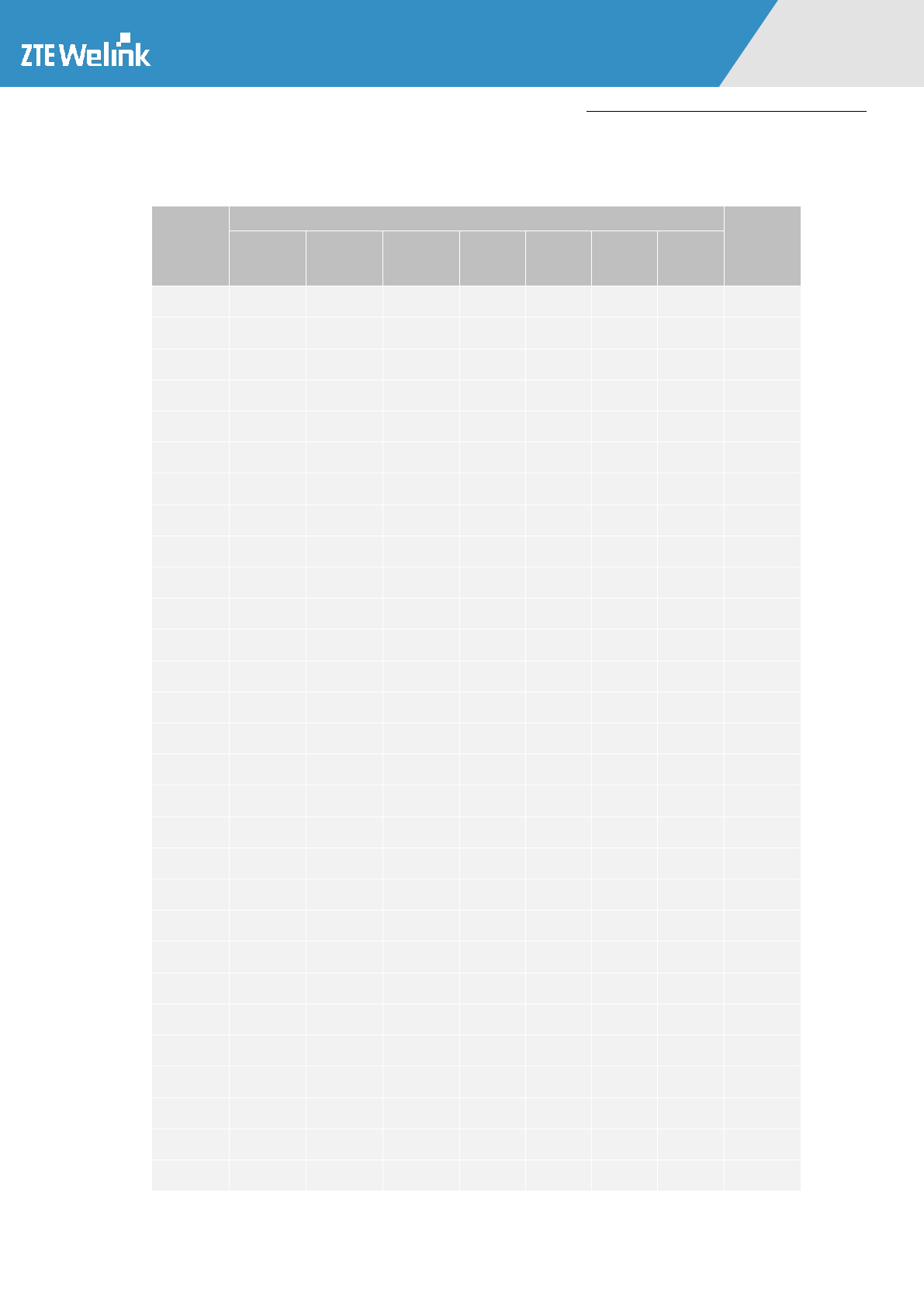
Hardware Development Guide of Module Product
All Rights reserved, No Spreading abroad without Permission of ZTEWelink 37
错误!未找到
用源。
ZM8620_V2
testing results might be slightly different. Take the actual situation as the reference.
Table 7–8 Receiving Sensitivity Reference Table
E-UTRA
Band
Channel bandwidth
Test value
(dBm)
1.4 MHz
(dBm)
3 MHz
(dBm)
5 MHz
(dBm)
10 MHz
(dBm)
15 MHz
(dBm)
20 MHz
(dBm)
Duplex
Mode
1
-
-
-100
-97
-95.2
-94
FDD
TBD
2
-102.7
-99.7
-98
-95
-93.2
-92
FDD
TBD
3
-101.7
-98.7
-97
-94
-92.2
-91
FDD
--
4
-104.7
-101.7
-100
-97
-95.2
-94
FDD
TBD
5
-103.2
-100.2
-98
-95
FDD
TBD
6
-100
-97
FDD
--
7
-98
-95
-93.2
-92
FDD
TBD
8
-102.2
-99.2
-97
-94
FDD
TBD
9
-99
-96
-94.2
-93
FDD
--
10
-100
-97
-95.2
-94
FDD
--
11
-100
-97
FDD
--
12
-101.7
-98.7
-97
-94
FDD
TBD
13
-97
-94
FDD
--
14
-99.2
-97
-94
FDD
--
…
--
17
-102.2
-99.2
-97
-94
FDD
--
18
-100
-97
-95.2
FDD
--
19
-100
-97
-95.2
FDD
--
20
-97
-94
-91.2
-90
FDD
--
21
-100
-97
-95.2
FDD
--
…
--
33
-100
-97
-95.2
-94
TDD
--
34
-100
-97
-95.2
-94
TDD
--
35
-106.2
-102.2
-100
-97
-95.2
-94
TDD
--
36
-106.2
-102.2
-100
-97
-95.2
-94
TDD
--
37
-100
-97
-95.2
-94
TDD
--
38
-100
-97
-95.2
-94
TDD
TBD
39
-100
-97
-95.2
-94
TDD
--
40
-100
-97
-95.2
-94
TDD
--

Hardware Development Guide of Module Product
All Rights reserved, No Spreading abroad without Permission of ZTEWelink 38
错误!未找到
用源。
ZM8620_V2
41
[-100]
[-97]
[-95.2]
[-94]
TDD
--
Note 1: The transmitter shall be set to maximum output power level as defined in clause 6.2.5 in the protocol
of 3GPP TS 36.101
Note 2: Reference measurement channel is specified A.3.2 with one sided dynamic OCNG Pattern OP.1
FDD/TDD as described in Annex A.5.1.1/A.5.2.1 in the protocol of 3GPP TS 36.101
Note 3: The signal power is specified per port
Note 4: For the UE which supports both Band 3 and Band 9 the reference sensitivity level of Band 3 + 0.5
dB is applicable for band 9
Note 5: For the UE which supports both Band 11 and Band 21 the reference sensitivity level is FFS.
7.3.3 Spurious Specification
Spurious emission meets 3GPP TS 36.101 protocol requirement.
The receiver spurious emission power refers to the spurious power generated or amplified by the module,
which is tested from the antenna connector.
The spurious emission shall meet the requirement of Table 7-9 and Table 7-10:
Table 7–9 General Requirement of Receiver Spurious Emission
Frequency range
Maximum level
Measurement bandwidth
9 kHz f < 150 kHz
-36 dBm
1 kHz
150 kHz f < 30 MHz
-36 dBm
10 kHz
30 MHz f < 1000
MHz
-36 dBm
100 kHz
1 GHz f < 12.75 GHz
-30 dBm
1 MHz
Table 7–10 UE Co-existence Spurious Emission Requirement
E-UTRA
Band
Spurious emission
Protected band
Frequency range
(MHz)
Level
(dBm)
Bandwidth
(MHz)
Comment
1
E-UTRA Band 1, 3, 7, 8, 9, 11,
34, 38, 40
FDL_low - FDL_high
-50
1
Frequency range
860-895
-50
1
Frequency range
1884.5-1919.6
-41
0.3
Note6,Note7
1884.5-1915.7
Note 6, Note8
E-UTRA band 33
1900-1920
-50
1
Note 3
E-UTRA band 39
1880-1920
-50
1
Note 3
2
E-UTRA Band 2, 4, 5, 10, 12,
13, 14, 17
FDL_low- FDL_high
-50
1

Hardware Development Guide of Module Product
All Rights reserved, No Spreading abroad without Permission of ZTEWelink 39
错误!未找到
用源。
ZM8620_V2
3
E-UTRA Band 1, 3, 7, 8, 9, 11,
33, 34, 38
FDL_low- FDL_high
-50
1
4
E-UTRA Band 2, 4, 5, 10, 12,
13, 14, 17
FDL_low- FDL_high
-50
1
5
E-UTRA Band 2, 4, 5, 10,
12, 13, 14, 17
FDL_low- FDL_high
-50
1
6
E-UTRA Band 1, 9, 11, 34
FDL_low- FDL_high
-50
1
Frequency range
860-875
-37
1
Frequency range
875-895
-50
1
Frequency range
1884.5-1919.6
-41
0.3
Note7
1884.5-1915.7
Note8
7
E-UTRA Band 1, 3, 7, 8, 33,
34
FDL_low- FDL_high
-50
1
E-UTRA Band 38
2570-2620
-50
1
Note 3
8
E-UTRA Band 1, 8, 7, 33,
34, 38, 39, 40
FDL_low- FDL_high
-50
1
E-UTRA band 3
1805-1830
-50
1
Note 4
E-UTRA band 3
1805-1880
-36
0.1
Note 2,4
E-UTRA band 3
1830-1880
-50
1
Note 4
E-UTRA band 7
2640-2690
-50
1
Note 4
E-UTRA band 7
2640-2690
-36
0.1
Note 2,4
9
E-UTRA Band 1, 9, 11, 34
FDL_low- FDL_high
-50
1
Frequency range
860-895
-50
1
Frequency range
1884.5-1919.6
-41
0.3
Note7
1884.5-1915.7
Note8
10
E-UTRA Band 2, 4, 5, 10, 12,
13, 14, 17
FDL_low- FDL_high
-50
1
11
E-UTRA Band 1, 9, 11, 34
FDL_low- FDL_high
-50
1
Frequency range
860-895
-50
1
Frequency range
1884.5-1919.6
-41
0.3
Note7
1884.5-1915.7
Note8
12
E-UTRA Band 2, 4, 5, 10,
12, 13, 14, 17
FDL_low- FDL_high
-50
1
13
E-UTRA Band 2, 4, 5, 10,
12, 13, 14, 17
FDL_low- FDL_high
-50
1
Frequency range
763-775
-35
0.00625
14
E-UTRA Band 2, 4, 5, 10,
12, 13, 14, 17
FDL_low- FDL_high
-50
1
Frequency range
763-775
-35
0.00625
17
E-UTRA Band 2, 4, 5, 10,
12, 13, 14, 17
FDL_low FDL_high
-50
1
…

Hardware Development Guide of Module Product
All Rights reserved, No Spreading abroad without Permission of ZTEWelink 40
错误!未找到
用源。
ZM8620_V2
33
E-UTRA Band 1, 3, 8, 34,
38, 39, 40
FDL_low- FDL_high
-50
1
Note 5
34
E-UTRA Band 1, 3, 7, 8, 9,
11, 33, 38,39, 40
FDL_low- FDL_high
-50
1
Note 5
Frequency range
860-895
-50
1
Frequency range
1884.5-1919.6
-41
0.3
Note7
1884.5-1915.7
Note8
35
36
37
38
E-UTRA Band 1,3, 33, 34
FDL_low- FDL_high
-50
1
39
E-UTRA Band 34, 40
FDL_low- FDL_high
-50
1
40
E-UTRA Band 1, 3, 33, 34, 39
FDL_low- FDL_high
-50
1
Note
1
FDL_low and FDL_high refer to each E-UTRA frequency band specified in Table 5.5-1 in the protocol
of 3GPP TS 36.101
2
As exceptions, measurements with a level up to the applicable requirements defined in Table 7-9 are
permitted for each assigned E-UTRA carrier used in the measurement due to 2nd or 3rd harmonic
spurious emissions. An exception is allowed if there is at least one individual RE within the
transmission bandwidth (see Figure 5.6-1 in the protocol of 3GPP TS 36.101) for which the 2nd or 3rd
harmonic, i.e. the frequency equal to two or three times the frequency of that RE, is within the
measurement bandwidth.
3
To meet these requirements some restriction will be needed for either the working band or protected
band
4
Requirements are specified in terms of E-UTRA sub-bands
5
For non synchronized TDD operation to meet these requirements some restriction will be needed for
either the working band or protected band
6
Applicable when NS_05 in section 6.6.3.3.1 in the protocol of 3GPP TS 36.101 is signaled by the
network.
7
Applicable when co-existence with PHS system working in. 1884.5-1919.6MHz.
8
Applicable when co-existence with PHS system working in 1884.5-1915.7MHz.
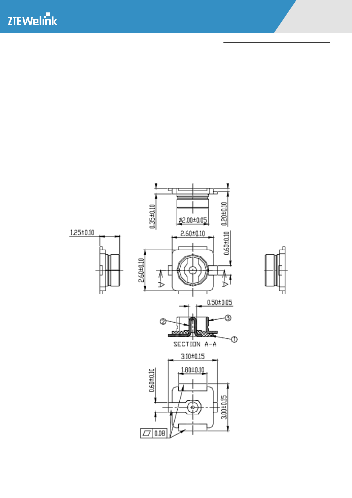
Hardware Development Guide of Module Product
All Rights reserved, No Spreading abroad without Permission of ZTEWelink 41
错误!未找到
用源。
ZM8620_V2
8 Antenna
8.1 RF Antenna Specification
8.1.1 Technical Parameter for the Main Antenna Connector
The main and diversity antenna is the product U.FL-R-SMT-1(80)(HRS)/ ECT818000071(ECT). The
Profile Dimensions is shown in Figure 8-1. If more technical parameter for the main antenna connector
is needed, please contact with ZTEWelink.
Figure 8–1 the Profile Dimensions
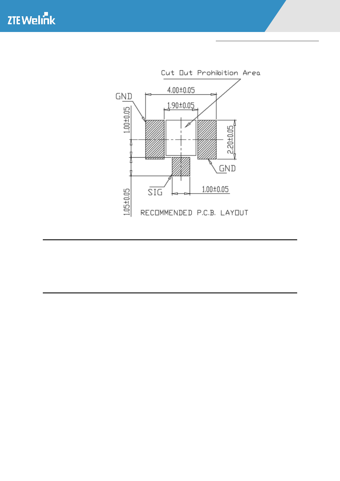
Hardware Development Guide of Module Product
All Rights reserved, No Spreading abroad without Permission of ZTEWelink 42
错误!未找到
用源。
ZM8620_V2
The PCB layout is shown in the Figure 8-2.
Figure 8–2 Recommended PCB layout
NOTE:
The radio frequency bases adopted by the antenna interface of ZM8620_V2 module is
U.FL-R-SMT-1(80)(HRS)/ECT818000071(ECT) at present instead of adopting 20429-001E MHF-A13
of I-PEX by ZM8620 before.
8.2 Proposal on Layout of Product in Terminal Product
The module layout among other terminal products should take full consideration of the electric magnetic
compatibility. As the types of terminal products vary and their circuit layouts are different, when
considering the module layout, we should reduce the electric magnetic interference from other devices
upon the module. Taking 3G Internet-access laptop as an example, during the layout of laptops, make
sure that the module is not adjacent to the switch power or the high-speed signal cable, and well protect
the cabling of these interference sources. At the same time, keep the antenna and the coaxial cables of
network cables and antenna far away from the interference sources. Keep the module away from the
devices that have a large heat-radiating capacity such as CPU, hard disk and south bridge, to guarantee
that heat can be radiated effectively.

Hardware Development Guide of Module Product
All Rights reserved, No Spreading abroad without Permission of ZTEWelink 43
错误!未找到
用源。
ZM8620_V2
8.3 Antenna Dimensions and Location
The dimensions of different terminal products are different, so they impose different requirements upon
the performance of antenna. The dimensions and location of antennas are also different. Taking 3G
Internet-access laptop as an example, it is recommended that the antenna be placed on the top of LCD.
8.4 Diversity Antenna Design
ZM8620_V2 supports diversity receiving function, and if it is necessary to support diversity, the
notebook needs to add diversity antenna. The design method of the diversity antenna is consistent with
the main antenna, and its efficiency index is allowed to reduce by 3dB. The isolation of the main antenna
and the diversity antenna is required to be bigger than 12dB.
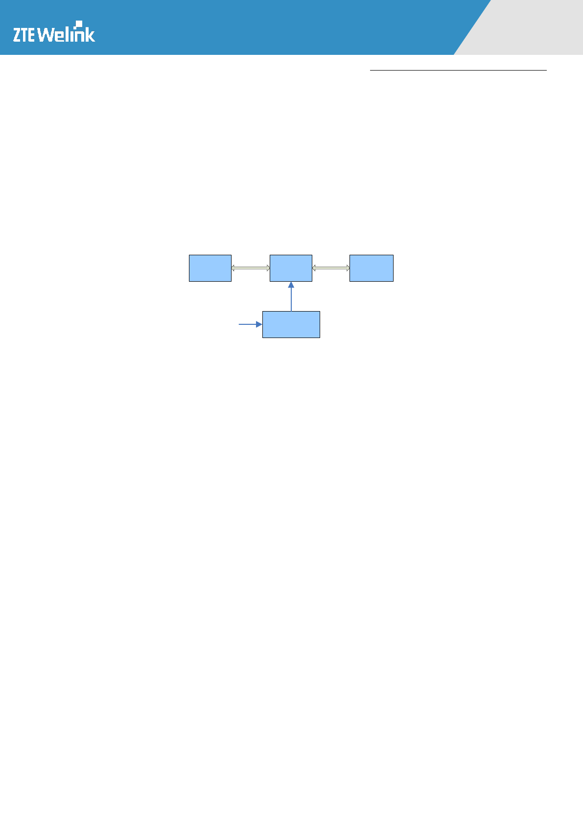
Hardware Development Guide of Module Product
All Rights reserved, No Spreading abroad without Permission of ZTEWelink 44
错误!未找到
用源。
ZM8620_V2
9 Debugging Environment and Method
In the process of the actual implementation, it is necessary to adopt the switching board to convert MINI
PCIE module interface into the standard USB interface to connect the host for debugging verification. It
is also necessary to connect external power supply adaptor to provide the module with sufficient current,
and the diagram for the switching board is as follows:
Module
board
Computer
host
Switching
board
Power supply
adapter
PCI Express
Mini Card
Interface USB Port
AC
Figure 9–1 The diagram for the switching board
9.1 Debugging Board
Figure 9-2 shows the module debugging & installation method. The debugging board is mainly used to
debug the basic functions of ZM8620_V2 module, such as downloading the JTAG program, resetting the
module, powering off and shutting down RF, LED indicator display, making a call or browsing web
pages via computer UI by inserting the USIM card into the switching board. The USB interface supplies
power to the debugging board, provides it to the module after LDO conversion, and directly supplies the
power to the module by the power socket on the board.
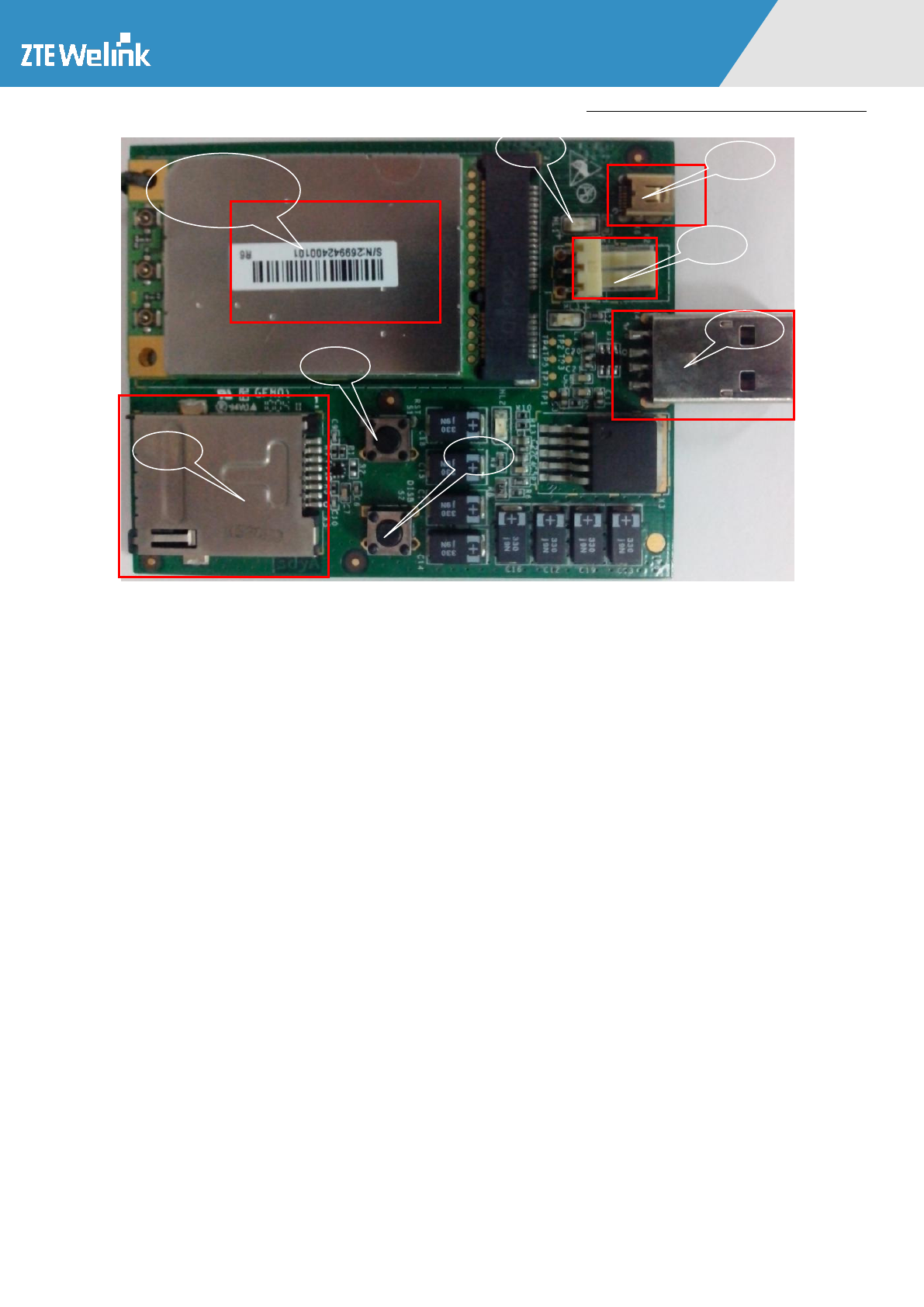
Hardware Development Guide of Module Product
All Rights reserved, No Spreading abroad without Permission of ZTEWelink 45
错误!未找到
用源。
ZM8620_V2
Figure 9–2 Debugging Board
Note: 1 – UIM card console; 2 –JTAG downloading interface; 3- DC power interface; 4 – USB interface; 5 – LED indicator; 6
- PON_RESET_N button (module resetting); 7 –W_DISABLE_N button (RF switch)
9.2 Interfaces on Debugging Board
9.2.1 JTAG Interface
The JTAG interface can be used to download and debug the firmware program. This interface is reserved
in the module of ZM8620_V2.
9.2.2 USB Interface
The USB2.0 interface on the debugging board is connected to the PCI-E interface on ZM8620_V2.
9.2.3 Power-supply Interface
The USB interface as illustrated in Figure 9-2 supplies power, provides the 3.3V power to the module
after LDO conversion, and directly supplies the 3.3V power to the module by the power socket on the
board.
Module
ZM8620_V2
1
2
3
4
5
6
7

Hardware Development Guide of Module Product
All Rights reserved, No Spreading abroad without Permission of ZTEWelink 46
错误!未找到
用源。
ZM8620_V2
9.2.4 USIM Card Console Interface
As shown in Figure 9-2, 1 the USIM card console is the 5PIN USIM card console on the conversion
board, connecting to: power, ground, UIM_DATA, USIM_CMD and UIM_CLK. It supports the
1.8V/3V USIM card.
9.2.5 PON_RESET_N Button
This button corresponds to the PON_RESET_N PIN of the PCI-E interfaced. The user presses the button
to reset the module.
9.2.6 W_DISABLE_N Button
This button corresponds to the W_DISABLE_N PIN of the PCI-E interface. The user presses this button
to enable or disconnect RF, so as to perform the debugging of this PIN.
9.2.7 LED Indicator
The LED indicator on the debugging board is connected to the LED_WWAN_N interface of
ZM8620_V2. By controlling the indicator, the user can debug the function of this interface.
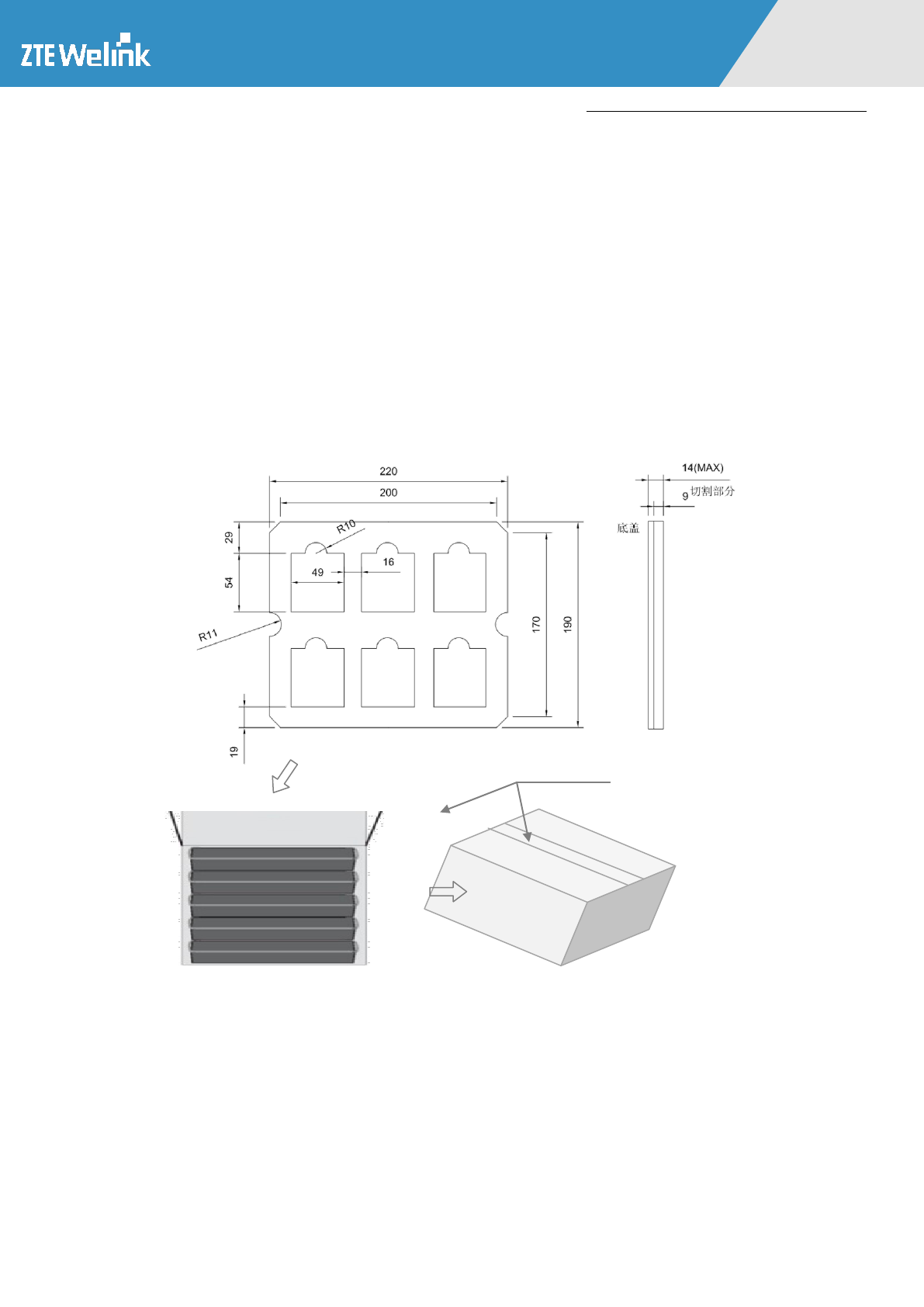
Hardware Development Guide of Module Product
All Rights reserved, No Spreading abroad without Permission of ZTEWelink 47
错误!未找到
用源。
ZM8620_V2
10 Package System
The ZM8620_V2 modules are wrapped with anti-static shielding bags, which is packaged on EPE trays of 6
pieces each. And these modules are put into cardboard box in a set of 10 trays. Each cardboard box is with 60
modules typically.
The package process of ZM8620_V2 modules is shown as the Figure below. The unit of dimensions is mm.
Figure 10–1 Package process of ZM8620_V2 modules
×10 trays
Cardboard box

Hardware Development Guide of Module Product
All Rights reserved, No Spreading abroad without Permission of ZTEWelink 48
错误!未找到
用源。
ZM8620_V2
11 Safety Information
The following safety precautions must be observed during all phases of the operation, such as usage, service
or repair of any cellular terminal incorporating ZM8620_V2 module. Manufacturers of the cellular terminal
should send the following safety information to users, operating personnel and to incorporate these guidelines
into all manuals supplied with the product.
The use of this product may be dangerous and has to be avoided in the following areas:
Where it can interfere with other electronic devices in environments such as hospitals, aircrafts, airports,
etc, switch off before boarding an aircraft. Make sure the cellular terminal is switched off in these areas.
The operation of wireless appliances in the hospitals, aircrafts and airports are forbidden to prevent
interference with communication systems.
Areas with potentially explosive atmospheres including fuelling areas, below decks on boats, fuel or
chemical transfer or storage facilities, areas where the air contains chemicals or particles such as
gasoline stations, oil refineries, etc make sure that wireless devices are turned off.
It‘s the responsibility of users to enforce other country regulations and the specific environment regulations.
And ZTEWelink does not take on any liability for customer failure to comply with these precautions.
12.NOTICE
Note1
:
This device complies with Part 15 of the FCC Rules
,
Operation is subject to the
following two conditions:
(1) this device may not cause harmful interference, and
(2) this device must accept any interference received, including interference
that may cause undesired operation.
Note2: This equipment has been tested and found to comply with the limits for a Class
B digital device, pursuant to Part 15 of the FCC Rules. These limits are designed to
provide reasonable protection against harmful interference in a residential installation.
This equipment generates, uses and can radiate radio frequency energy and, if not
installed and used in accordance with the instructions, may cause harmful interference
to radio communications. However, there is no guarantee that interference will not
occur in a particular installation. If this equipment does cause harmful interference to
radio or television reception, which can be determined by turning the equipment off and
on, the user is encouraged to try to correct the interference by one or more of the
following measures:
Reorient or relocate the receiving antenna.
Increase the separation between the equipment and receiver.
Connect the equipment into an outlet on a circuit different from that to which the
receiver is connected.
Consult the dealer or an experienced radio/TV technician for help.
Note3: For EUT which intended use is at least 20 cm between human body and antenna.
Note4: Label of The End Product
The final end product must be labeled in a visible are with the following
Contains TX
FCC ID:SRQ-ZM8620
.The FCC part 15.19 statement below has to also be available on
the label:This device complies with Part 15 of FCC rules.Operation is subject to the foll
owing two conditions: (1) This device may not cause harmful interference, and (2) this
device must accept any interference received, including interference that may cause u
ndesired operation. To comply with FCC regulations limiting both maximum RF output
power and human exposure to RF radiation.
A user manual with the end product must clearly indicate the operating requirements a
nd conditions that must be observed to ensure compliance with current FCC RF expos
ure guidelines. The end product with an Module may also need to pass the FCC Part 1
5 unintentional emission testing requirements and be properly authorized per FCC Part
15. Note:If this module is intended for use in a portable device,you are responsible for
separate approval to satify the SAR requirements of FCC Part 2.1093.