ZTE ZTEMF206A HSPA LGA Module User Manual
ZTE Corporation HSPA LGA Module Users Manual
UserManual.wiki
>
ZTE
>
ZTEMF206A User Manual
>
Users Manual
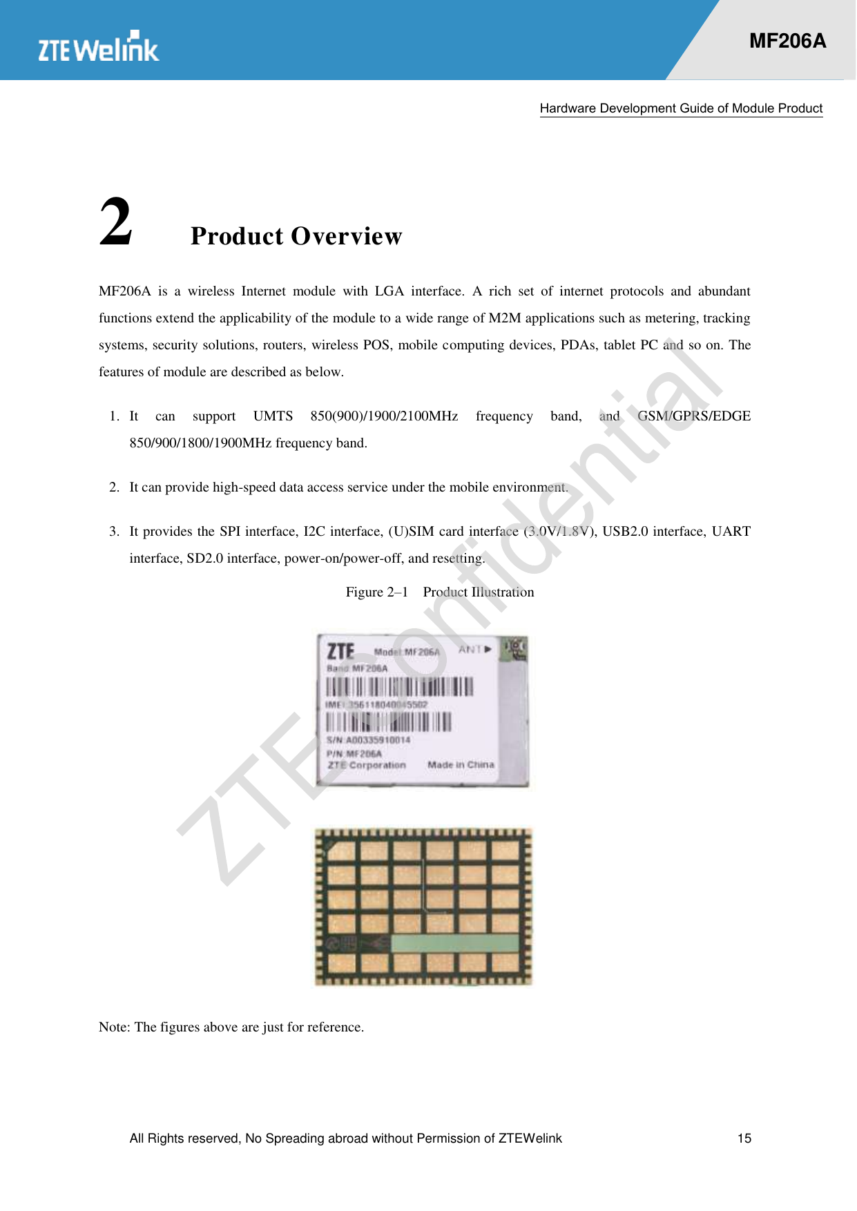
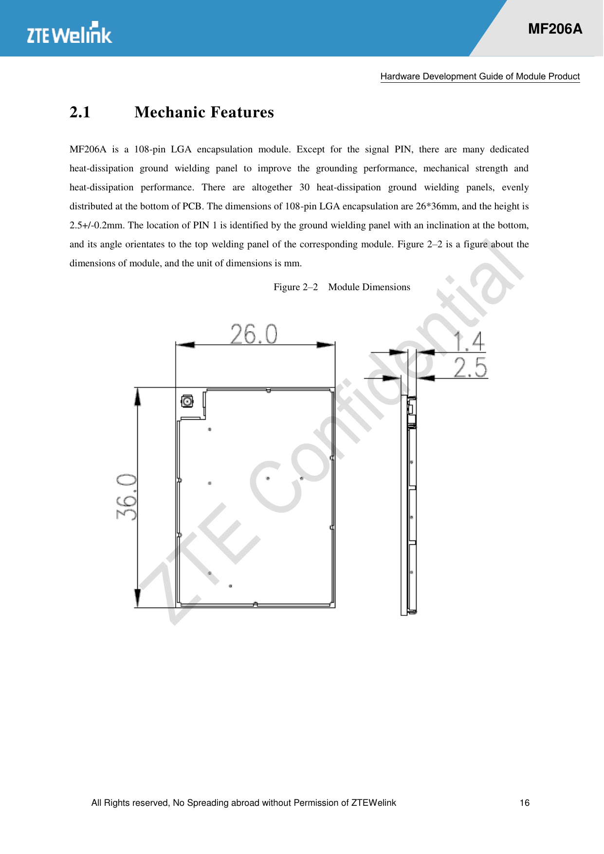
Contents
1.
HSPA LGA Module User Manual-110301
2.
Users Manual
Users Manual
Navigation menu
Upload a User Manual
Namespaces
Wiki Guide
HTML
PDF
Info
Views
User Manual
Discussion / Help
Navigation
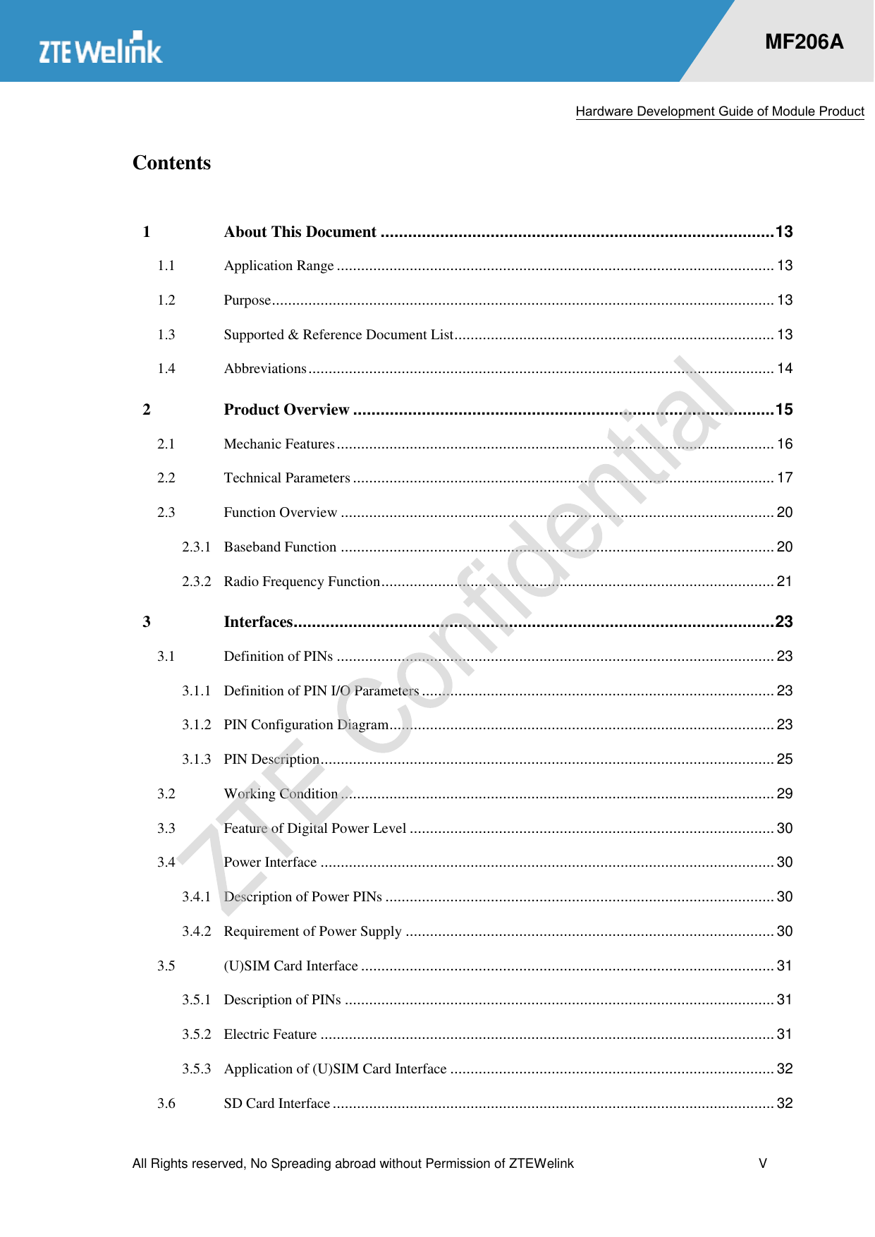
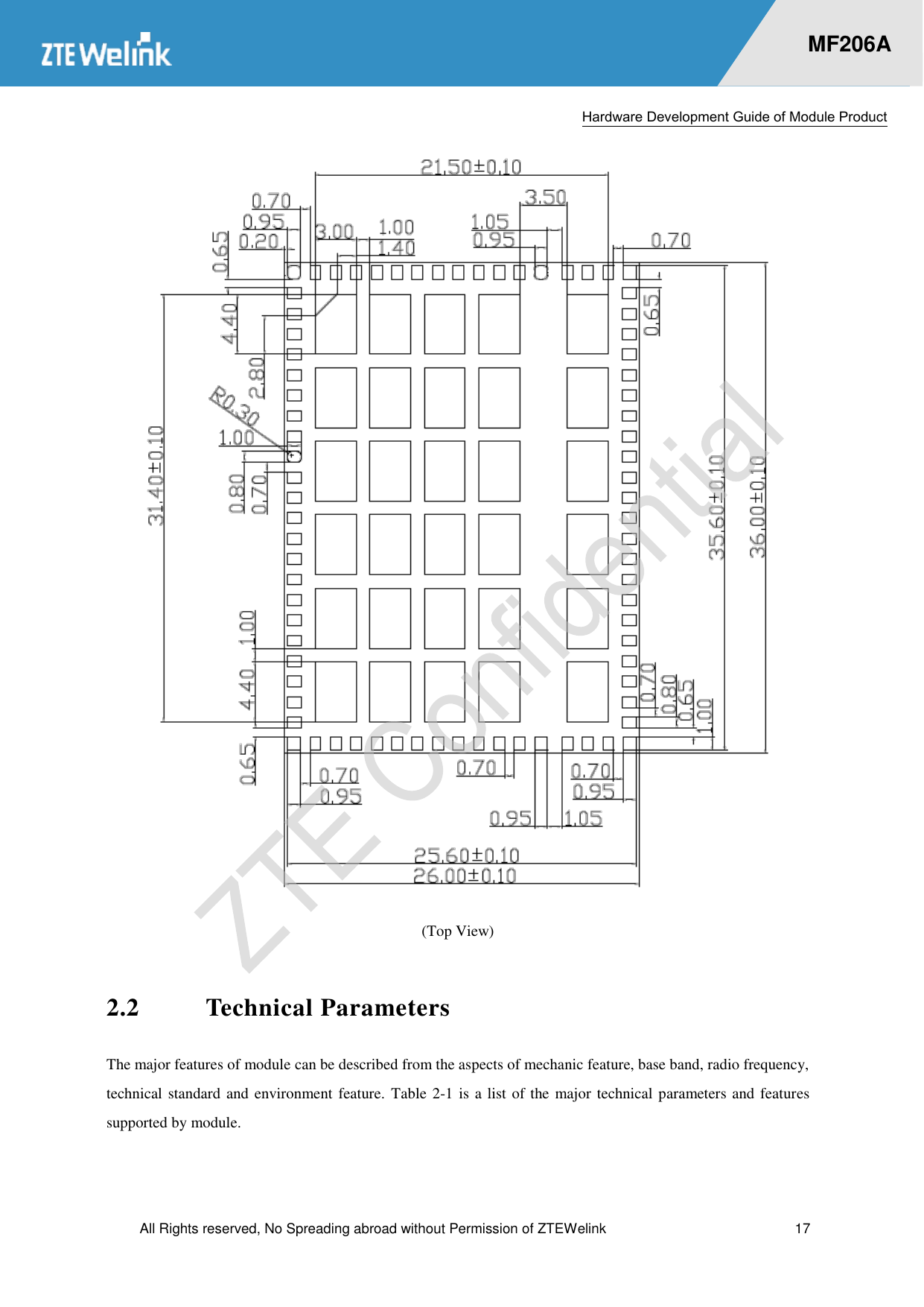
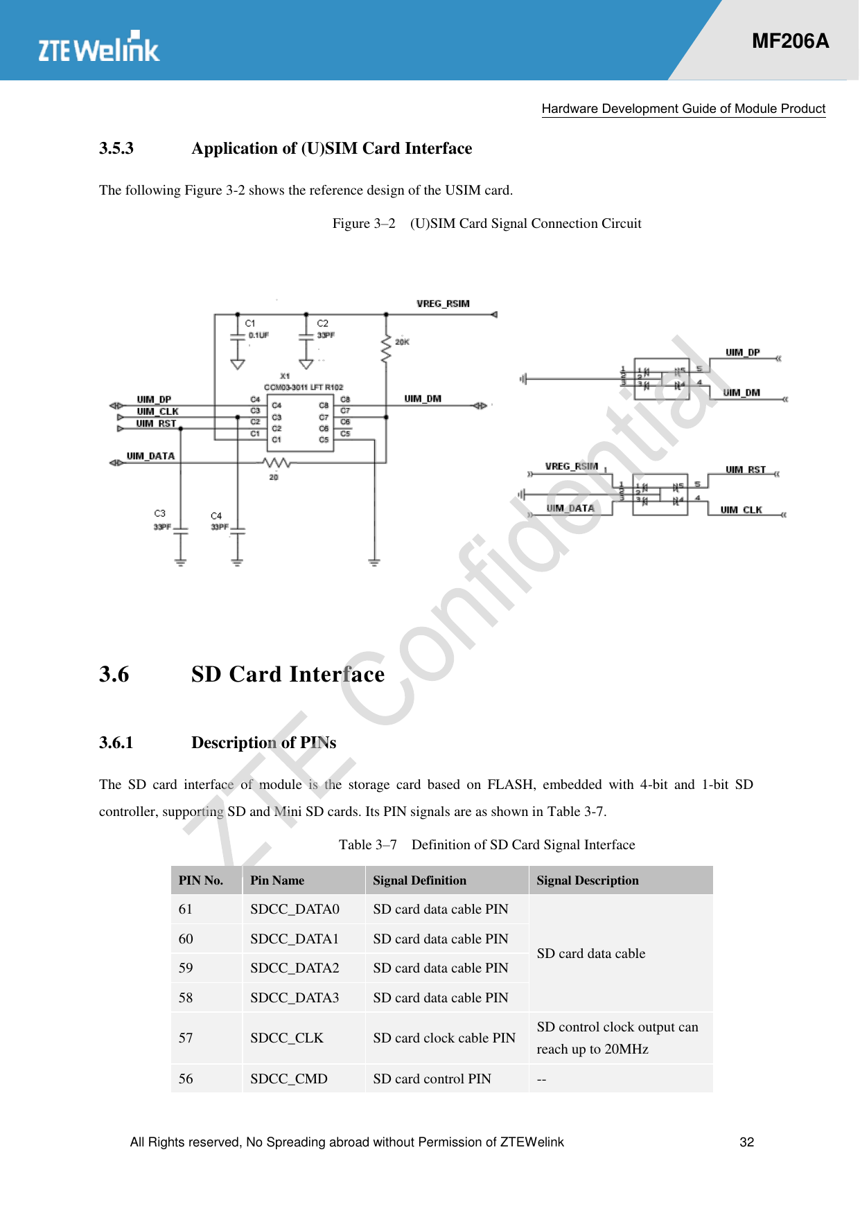
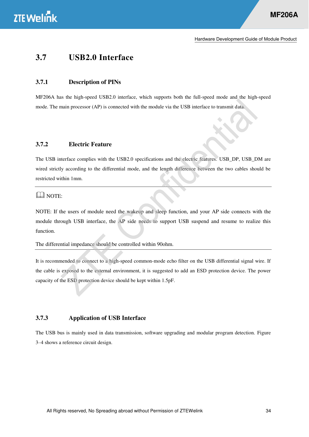
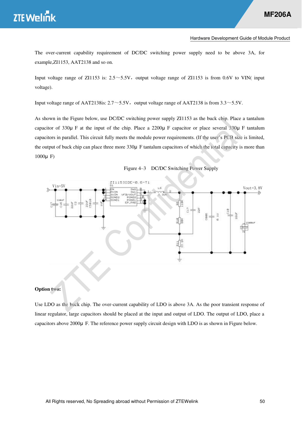
![Hardware Development Guide of Module Product All Rights reserved, No Spreading abroad without Permission of ZTEWelink 33 MF206A 55 VREG_MMC SD card power 3V 3.6.2 Electric Feature SDCC_CLK: Clock signal, host2device, default is 0~25MHz. SDCC_CMD: Command/response, two-way: the command can be sent from the host to a single card/all cards, the response is sent from a single card/all cards to the host. SDCC_DATA[3..0]: Data cable, two-way, default is 0~12.5MB/sec. 3.6.3 Application of SD Card Interface Figure 3–3 is the reference design diagram for the SD interface. The detection of SD card adopts the polling mode of DATA3 signal cable to judge whether T card is inserted or not. Figure 3–3 SD Typical Application Circuit](https://usermanual.wiki/ZTE/ZTEMF206A.Users-Manual/User-Guide-3115887-Page-34.png)