Contents
- 1. HSPA LGA Module User Manual-110301
- 2. Users Manual
Users Manual

Hardware Development Guide of
Module Product
Version 2.5, 2015-06-18
MF206A
Hardware Development Guide of Module Product
All Rights reserved, No Spreading abroad without Permission of ZTEWelink I
MF206A
Legal Information
By receiving the document from Shenzhen ZTEWelink Technology Co., Ltd (shortly referred to as
ZTEWelink), you are deemed to have agreed to the following terms. If you don’t agree to the
following terms, please stop using the document.
Copyright © 2013 Shenzhen ZTEWelink Technology Co., Ltd. All rights reserved. The document
contains ZTEWelink’s proprietary information. Without the prior written permission of ZTEWelink,
no entity or individual is allowed to reproduce, transfer, distribute, use and disclose this document or
any image, table, data or other information contained in this document.
is the registered trademark of ZTEWelink. The name and logo of ZTEWelink are
ZTEWelink’s trademark or registered trademark. Meanwhile, ZTEWelink is granted to use ZTE
Corporation’s registered trademark. The other products or company names mentioned in this
document are the trademark or registered trademark of their respective owner. Without the prior
written permission of ZTEWelink or the third-party oblige, no one is allowed to read this document.
The product meets the design requirements of environmental protection and personal security. The
storage, use or disposal of products should abide by the product manual, relevant contract or the laws
and regulations of relevant country.
ZTEWelink reserves the right to make modifications on the product described in this document
without prior notice, and keeps the right to revise or retrieve the document any time.
If you have any question about the manual, please consult the company or its distributors promptly.

Hardware Development Guide of Module Product
All Rights reserved, No Spreading abroad without Permission of ZTEWelink II
MF206A
Revision History
Version
Date
Description
1.0
2010-11-18
Initial version
2.0
2011-3-15
Chapter 1:
1. Add the application range and compilation purpose
Chapter 2:
1. Update Table2-1
2. Add the introduction of baseband function and radio frequency;
add the frame structure
Chapter 3:
1. Add the definition of PIN I/O parameter, and provide the
description of PINs
2. Add the feature of interface PWL
Chapter 4:
1. Add the chapter
Chapter 5:
1. Update the RF sourced index and source less index
Chapter 6:
1. Update the testing standard and testing environment
Chapter 7:
1. Add the chapter
Chapter 8:
1. Add the chapter
2.1
2013-03-26
1. Modify the logo of cover and page footer
2. Modify Legal Information
3. Modify some errors in the Table 2-2 of Working Frequency Band
4. Update the Table 1-1 of Supported Document List
5. Modify the chapter of 7.7 of Recommended Upgrade Methods
6. Modify the Figure 7-1 of Main Antenna RF Connector Interface
to erase the IMEI in picture
7. Modify the test result in Table 6-6
8. Modify the name of Table 5-1 to sourceless
2013-05-31
9. Release as Version 2.1
2.2
2013-12-09
1. Modify the Figure 2-2.
2. Add the contact information
Hardware Development Guide of Module Product
All Rights reserved, No Spreading abroad without Permission of ZTEWelink III
MF206A
Version
Date
Description
3. Update Document Format
2.3
2013-12-30
1. Add the profile dimensions of RF antenna console
2. Modify part 7.3 of RF Circuit Design
2.4
2014-06-30
1. Update the legal information
2. Add the NOTE in chapter 1.2
3. Update Table 1-1 of Reference Document List
4. Update Table 2-1 of Major Technical Parameters
5. Update Table 3-1 of PIN Parameters
6. Add Table 3–3 of The Mandatory Pins of Module
7. Update Figure 3-3 of SD Typical Application Circuit
8. Modify chapter 3.10 of Power-on/Power-off & Reset Signal
9. Update Figure 3-16 of Reference Circuit of Status Indicator
10. Modify chapter 4.2 of Working Current
11. Move the chapter 4.2 and 4.3 of Power-on/Power-off Flow in the
former document to chapter 3.10
12. Modify Index of RF under UMTS & GPRS/GSM/EDGE Mode
in chapter 5.1 and 5.2
13. Add the NOTE in chapter 6.3
14. Add Figure 9-1 of Recommended PCB Wielding Panel Design
15. Modify Figure 5–1 of Main Antenna RF Connector Interface
16. Modify chapter 10.2 of Furnace Temperature Curve
17. Add chapter 11 of Safety Information
18. Add the chapter 10.3 of Package System
2.5
2015-06-15
1. Add the description of Suspend and Resume of module in
chapter 3.10 &3.7
2. Update the figures of module
Hardware Development Guide of Module Product
All Rights reserved, No Spreading abroad without Permission of ZTEWelink IV
MF206A
Contact Information
Post
9/F, Tower A, Hans Innovation Mansion,
North Ring Rd., No.9018, Hi-Tech Industrial Park,
Nanshan District, Shenzhen. P.R.China
Web
www.ztewelink.com
Phone
+86-755-26902600
E-Mail
ztewelink@zte.com.cn
Note: Consult our website for up-to-date product descriptions, documentation, application notes, firmware
upgrades, troubleshooting tips, and press releases
Besides, ZTEWelink provides various technical support ways to the customers, such as support by phone,
website, instant messaging, E-mail and on-site.

Hardware Development Guide of Module Product
All Rights reserved, No Spreading abroad without Permission of ZTEWelink V
MF206A
Contents
1 About This Document ...................................................................................... 13
1.1 Application Range ............................................................................................................ 13
1.2 Purpose ............................................................................................................................ 13
1.3 Supported & Reference Document List ............................................................................... 13
1.4 Abbreviations ................................................................................................................... 14
2 Product Overview ............................................................................................ 15
2.1 Mechanic Features ............................................................................................................ 16
2.2 Technical Parameters ........................................................................................................ 17
2.3 Function Overview ........................................................................................................... 20
2.3.1 Baseband Function ........................................................................................................... 20
2.3.2 Radio Frequency Function ................................................................................................. 21
3 Interfaces ......................................................................................................... 23
3.1 Definition of PINs ............................................................................................................ 23
3.1.1 Definition of PIN I/O Parameters ....................................................................................... 23
3.1.2 PIN Configuration Diagram ............................................................................................... 23
3.1.3 PIN Description ................................................................................................................ 25
3.2 Working Condition ........................................................................................................... 29
3.3 Feature of Digital Power Level .......................................................................................... 30
3.4 Power Interface ................................................................................................................ 30
3.4.1 Description of Power PINs ................................................................................................ 30
3.4.2 Requirement of Power Supply ........................................................................................... 30
3.5 (U)SIM Card Interface ...................................................................................................... 31
3.5.1 Description of PINs .......................................................................................................... 31
3.5.2 Electric Feature ................................................................................................................ 31
3.5.3 Application of (U)SIM Card Interface ................................................................................ 32
3.6 SD Card Interface ............................................................................................................. 32

Hardware Development Guide of Module Product
All Rights reserved, No Spreading abroad without Permission of ZTEWelink VI
MF206A
3.6.1 Description of PINs .......................................................................................................... 32
3.6.2 Electric Feature ................................................................................................................ 33
3.6.3 Application of SD Card Interface ....................................................................................... 33
3.7 USB2.0 Interface .............................................................................................................. 34
3.7.1 Description of PINs .......................................................................................................... 34
3.7.2 Electric Feature ................................................................................................................ 34
3.7.3 Application of USB Interface............................................................................................. 34
3.8 SPI (Serial Peripheral Interface) Bus Interface .................................................................... 35
3.8.1 Description of PINs .......................................................................................................... 35
3.8.2 Electric Feature ................................................................................................................ 35
3.9 I2C Bus ........................................................................................................................... 36
3.9.1 Description of PINs .......................................................................................................... 36
3.9.2 Electric Feature ................................................................................................................ 37
3.10 UART Interface ................................................................................................................ 38
3.10.1 Description of PINs .......................................................................................................... 38
3.10.2 Electric Feature ................................................................................................................ 38
3.11 JTAG (Joint Test Action Group) Interface .......................................................................... 39
3.11.1 Description of PINs .......................................................................................................... 39
3.11.2 Application of JTAG Interface ........................................................................................... 40
3.12 Power-on/Power-off & Reset Signal ................................................................................... 40
3.12.1 Description of PINs .......................................................................................................... 40
3.12.2 Power-on/Power-off Flow ................................................................................................. 42
3.12.3 Resetting Flow ................................................................................................................. 43
3.13 Interactive Application Interface ........................................................................................ 44
3.13.1 Description of PINs .......................................................................................................... 44
3.13.2 Interface Application ........................................................................................................ 45
3.14 LED Indicator Interface .................................................................................................... 45
3.14.1 Description of PINs .......................................................................................................... 45
3.14.2 Interface Application ........................................................................................................ 46

Hardware Development Guide of Module Product
All Rights reserved, No Spreading abroad without Permission of ZTEWelink VII
MF206A
4 Power Interface Design Guideline ..................................................................... 47
4.1 General Design Rules........................................................................................................ 47
4.2 Power Supply Requirement ............................................................................................... 47
4.3 Circuit Requirements of Power Supply Output .................................................................... 48
4.4 Recommended Power Reference Circuit ............................................................................. 49
4.5 PCB Layout Guideline of Power Supply ............................................................................. 51
5 RF Antenna Design Guide ................................................................................ 53
5.1 Antenna Types ................................................................................................................. 53
5.2 Antenna RF Cable and RF Connector ................................................................................. 53
5.2.1 RF Connector ................................................................................................................... 53
5.2.2 RF Cable.......................................................................................................................... 56
5.3 Design of Antenna ............................................................................................................ 57
5.3.1 Preliminary Antenna Evaluation ........................................................................................ 57
5.3.2 Suggested Antenna Location ............................................................................................. 58
5.3.3 Suggested Antenna Occupancy Space ................................................................................ 58
5.3.4 Matching Circuit of Antenna ............................................................................................. 58
5.3.5 Type of Antenna RF Cable & RF Connector ....................................................................... 59
5.4 Recommended Antenna Manufacturers .............................................................................. 60
5.5 PCB line guidelines .......................................................................................................... 60
5.6 Suggestions for EMC & ESD Design ................................................................................. 61
5.6.1 EMC Design Requirements ............................................................................................... 61
5.6.2 ESD Design Requirements ................................................................................................ 62
5.7 Antenna Indexes ............................................................................................................... 62
5.7.1 Passive Indexes ................................................................................................................ 63
5.7.2 Active Indexes ................................................................................................................. 63
5.7.3 Test Methods for Whole-Set Antenna OTA ........................................................................ 64
6 Electric Feature ............................................................................................... 65
6.1 Power Supply ................................................................................................................... 65

Hardware Development Guide of Module Product
All Rights reserved, No Spreading abroad without Permission of ZTEWelink VIII
MF206A
6.2 Working Current .............................................................................................................. 65
7 Technical Index of Radio Frequency ................................................................. 68
7.1 Index of RF under UMTS Mode ........................................................................................ 68
7.1.1 UMTS (WCDMA) ............................................................................................................ 68
7.1.2 Acquiring Radio Frequency Index ...................................................................................... 69
7.1.3 Maximum Transmission Power .......................................................................................... 69
7.1.4 Receiving Sensibility ........................................................................................................ 69
7.1.5 Spurious Emission Index ................................................................................................... 70
7.2 Index of RF under GPRS/GSM/EDGE Mode ...................................................................... 70
7.2.1 Output Transmission Power ............................................................................................... 70
7.2.2 Receiving Sensibility ........................................................................................................ 71
7.2.3 Spurious Emission Index ................................................................................................... 71
8 Related Test & Test Standard ........................................................................... 72
8.1 Testing Reference ............................................................................................................. 72
8.2 Description of Testing Environment ................................................................................... 73
8.3 Reliability Testing Environment ........................................................................................ 74
8.4 Reliability Testing Result .................................................................................................. 75
9 Design Guide ................................................................................................... 77
9.1 General Design Rule & Requirement .................................................................................. 77
9.2 Suggestions for PCB Wielding Panel Design ...................................................................... 77
9.3 Suggestions for Heat-dissipation Design ............................................................................. 78
9.4 Recommended Product Upgrading Plan .............................................................................. 79
10 Manufacturing Guide ....................................................................................... 80
10.1 Design of Steel Mesh ........................................................................................................ 80
10.2 Furnace Temperature Curve .............................................................................................. 81
10.3 Package System ................................................................................................................ 83
11 Safety Information ........................................................................................... 85

Hardware Development Guide of Module Product
All Rights reserved, No Spreading abroad without Permission of ZTEWelink IX
MF206A
Figures
Figure 2–1 Product Illustration ............................................................................................ 15
Figure 2–2 Module Dimensions ........................................................................................... 16
Figure 2–3 System Connection Structure .............................................................................. 21
Figure 3–1 PIN Configuration Diagram ................................................................................ 24
Figure 3–2 (U)SIM Card Signal Connection Circuit ............................................................... 32
Figure 3–3 SD Typical Application Circuit ........................................................................... 33
Figure 3–4 USB Typical Circuit Application ......................................................................... 35
Figure 3–5 SPI Bus Sequence Chart ..................................................................................... 36
Figure 3–6 I2C Reference Circuit Diagram ........................................................................... 37
Figure 3–7 Module Serial Port & AP Application Processor .................................................... 39
Figure 3–9 Turn on the Module Using Driving Circuit ............................................................ 41
Figure 3–10 Resetting the Module Using Driving Circuit ........................................................ 41
Figure 3–11 Power-on Sequence Chart of Module.................................................................. 42
Figure 3–12 Power-off Sequence Chart of Module ................................................................. 43
Figure 3–13 Module Resetting Flow ..................................................................................... 44
Figure 3–14 Timing of Resetting Module .............................................................................. 44
Figure 3–16 Reference Circuit of Status Indicator .................................................................. 46
Figure 4–1 Power Supply Current and Voltage Change under EDGE/GPRS .............................. 48
Figure 4–2 Add storage capacitor to Module power supply terminal ......................................... 49
Figure 4–3 DC/DC Switching Power Supply ......................................................................... 50
Figure 4–4 LDO Power Supply ............................................................................................ 51
Figure 5–1 Main Antenna RF Connector Interface ................................................................. 54
Figure 5–2 Interface of Main Antenna and GPS Antenna Welding Pad ..................................... 54
Figure 5–3 RF Interface Testing Console .............................................................................. 55
Figure 5–4 Profile Dimensions of RF antenna console ............................................................ 55
Figure 5–5 Recommended Receptacles Mode for MF206A ..................................................... 57
Figure 5–6 Transition Circuit ............................................................................................... 59
Figure 5–7 The OTA test system of CTIA ............................................................................. 64
Figure 9–1 Recommended PCB Wielding Panel Design.......................................................... 78

Hardware Development Guide of Module Product
All Rights reserved, No Spreading abroad without Permission of ZTEWelink X
MF206A
Figure 10–1 Recommended Pattern of Steel Mesh on Wielding panel ....................................... 80
Figure 10–2 Furnace Temperature Curve Reference Diagram .................................................. 82
Figure 10–3 The dimensions of Package tray ......................................................................... 83
Figure 10–4 Package process of modules .............................................................................. 84

Hardware Development Guide of Module Product
All Rights reserved, No Spreading abroad without Permission of ZTEWelink XI
MF206A
Tables
Table 1–1 Reference Document List ..................................................................................... 14
Table 1–2 Abbreviation List ................................................................................................ 14
Table 2–1 Major Technical Parameters ................................................................................. 18
Table 2–2 Working Frequency Band .................................................................................... 21
Table 3–1 PIN Parameters ................................................................................................... 23
Table 3–2 PIN Interface Definition ...................................................................................... 25
Table 3–3 Mandatory Pins of Module ................................................................................... 28
Table 3–4 Working Condition ............................................................................................. 29
Table 3–5 Power Level Range of Digital Signal ..................................................................... 30
Table 3–6 Definition & Description of (U)SIM Card Signal Group .......................................... 31
Table 3–7 Definition of SD Card Signal Interface .................................................................. 32
Table 3–8 Definition of SPI Signal ....................................................................................... 35
Table 3–9 Definition of UART Signal .................................................................................. 38
Table 3–10 Definition of JTAG Signal ................................................................................. 39
Table 3–11 Power-on/Power-off Time .................................................................................. 43
Table 3–12 Interactive Application Interface ......................................................................... 44
Table 3–13 Definition of LED PIN Signal ............................................................................. 45
Table 3–14 Definition of Indicator Status .............................................................................. 46
Table 5–1 The Cable Consumption ...................................................................................... 56
Table 5–2 Passive Indexes of Main Antennas on PAD Products ............................................... 63
Table 5–3 ZTEWelink Indexes for Mobile Terminal Devices .................................................. 63
Table 6–1 Input Voltage ..................................................................................................... 65
Table 6–2 Averaged standby DC power consumption ............................................................. 65
Table 6–3 Averaged idle mode DC power consumption .......................................................... 66
Table 6–4 Averaged DC power consumption in working state ................................................. 66
Table 7–1 Maximum Transmission Power ............................................................................ 69
Table 7–2 Reference Table of Receiving Sensitivity ............................................................... 69
Table 7–3 Spurious Emission Index...................................................................................... 70
Table 7–4 Output Transmission Power of GSM850/900/1800/1900 (GMSK) ............................ 70

Hardware Development Guide of Module Product
All Rights reserved, No Spreading abroad without Permission of ZTEWelink XII
MF206A
Table 7–5 Reference Table of Receiving Sensitivity ............................................................... 71
Table 8–1 Testing Standard ................................................................................................. 72
Table 8–2 Testing Environment ........................................................................................... 73
Table 8–3 Testing Instrument & Device ................................................................................ 74
Table 8–4 Reliability Features ............................................................................................. 74
Table 8–5 Temperature Testing Result Under Windless Environment ....................................... 75
Table 8–6 High/Low-temperature Running & Storage Testing Result ....................................... 75
Table 10–1 Curve Temperature Curve Parameter Setting ........................................................ 81

Hardware Development Guide of Module Product
All Rights reserved, No Spreading abroad without Permission of ZTEWelink 13
MF206A
1 About This Document
1.1 Application Range
This document is applicable as the hardware development guide of MF206A WCDMA module products. The
user can design the product according to the requirement and guidance in this document. It is only applicable for
the hardware application and development of MF206A WCDMA module products.
1.2 Purpose
This document provides the hardware solutions and development fundamentals for a product with the
ZTEWelink module. By reading this document, the user can have an overall knowledge of MF206A and a clear
understanding of the technical parameters. With this document, the user can successfully fulfill the application
and development of wireless 3G Internet product or equipment.
Besides the product features and technical parameters, this document also provides the product reliability tests
and related testing standards, service function implementation flow, RF performance indexes and a guide on the
design of user circuits, to provide the user with a complete design reference.
NOTE:
To ensure the module manufacturing and welding quality, do as the chapter 10 of Manufacturing Guide in
this document. The force on the squeegee should be adjusted so as to produce a clean stencil surface on a
single pass and ensure the module soldering quality
1.3 Supported & Reference Document List
Besides the hardware development document, ZTEWelink also provides the board operation guide, software
development guide and upgrading plan guide of MF206A. Table 1–1 is the list of supported documents.

Hardware Development Guide of Module Product
All Rights reserved, No Spreading abroad without Permission of ZTEWelink 14
MF206A
Table 1–1 Reference Document List
NO.
Document Name
1
ZTEWelink LGA Type Ⅱ Module Dev Board User Guide.pdf
2
ZTEWelink Software Development Guide of Module
Products.pdf
3
AT Commands reference guide for ZTEWelink WCDMA
Modules.pdf
4
ZTEWelink SMT & Baking User Guide of Module Products.pdf
1.4 Abbreviations
Table 1–2 is a list of abbreviations involved in this document, as well as the English full names.
Table 1–2 Abbreviation List
Abbreviations
Full Name
AP
Another name of DTE
BER
Bit Error Rate
DL
Downlink
DPCH
Dedicated Physical Channel
ESD
Electro-Static discharge
ECT
Electric Connector Technology CO.,LTD
GPRS
General Packet Radio Service
GSM
Global Standard for Mobile Communications
I/O
Input/output
LED
Light Emitting Diode
PWL
Power Level
SIM
Subscriber Identification Module
SMT
Surface Mount Technology
SPI
Serial Peripheral Interface
UMTS
Universal Mobile Telecommunication System
WCDMA
Wideband Code Division Multi Access
Hardware Development Guide of Module Product
All Rights reserved, No Spreading abroad without Permission of ZTEWelink 15
MF206A
2 Product Overview
MF206A is a wireless Internet module with LGA interface. A rich set of internet protocols and abundant
functions extend the applicability of the module to a wide range of M2M applications such as metering, tracking
systems, security solutions, routers, wireless POS, mobile computing devices, PDAs, tablet PC and so on. The
features of module are described as below.
1. It can support UMTS 850(900)/1900/2100MHz frequency band, and GSM/GPRS/EDGE
850/900/1800/1900MHz frequency band.
2. It can provide high-speed data access service under the mobile environment.
3. It provides the SPI interface, I2C interface, (U)SIM card interface (3.0V/1.8V), USB2.0 interface, UART
interface, SD2.0 interface, power-on/power-off, and resetting.
Figure 2–1 Product Illustration
Note: The figures above are just for reference.
Hardware Development Guide of Module Product
All Rights reserved, No Spreading abroad without Permission of ZTEWelink 16
MF206A
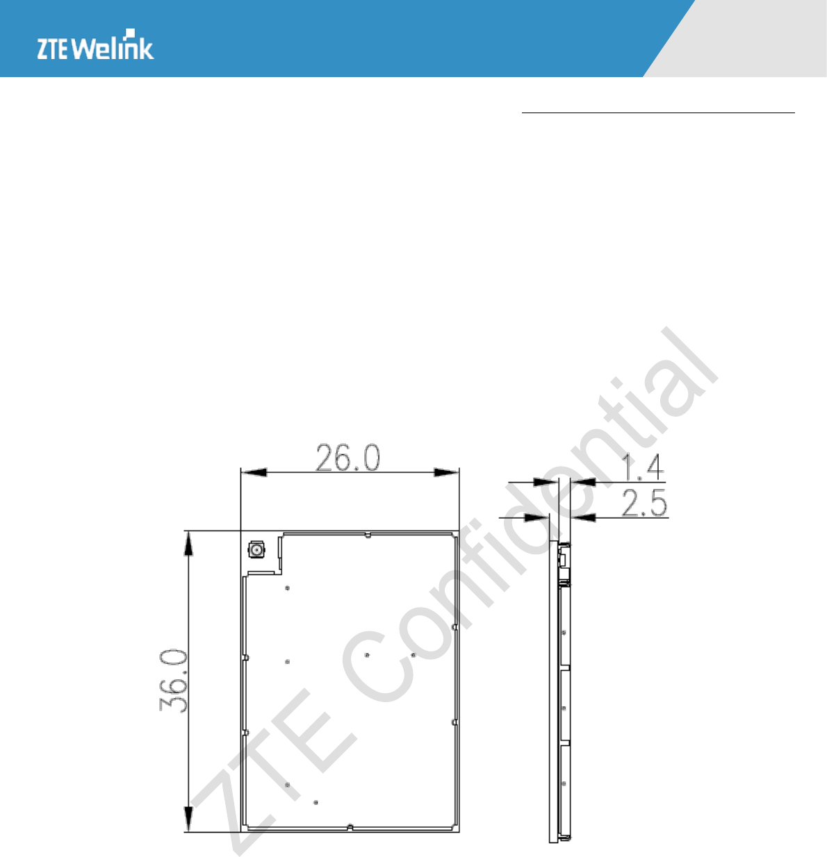
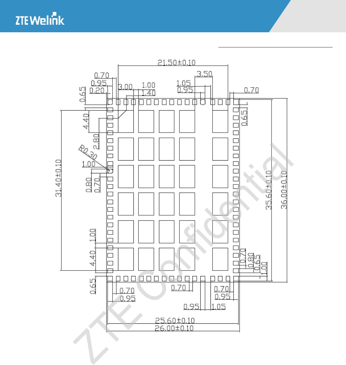
2.1 Mechanic Features
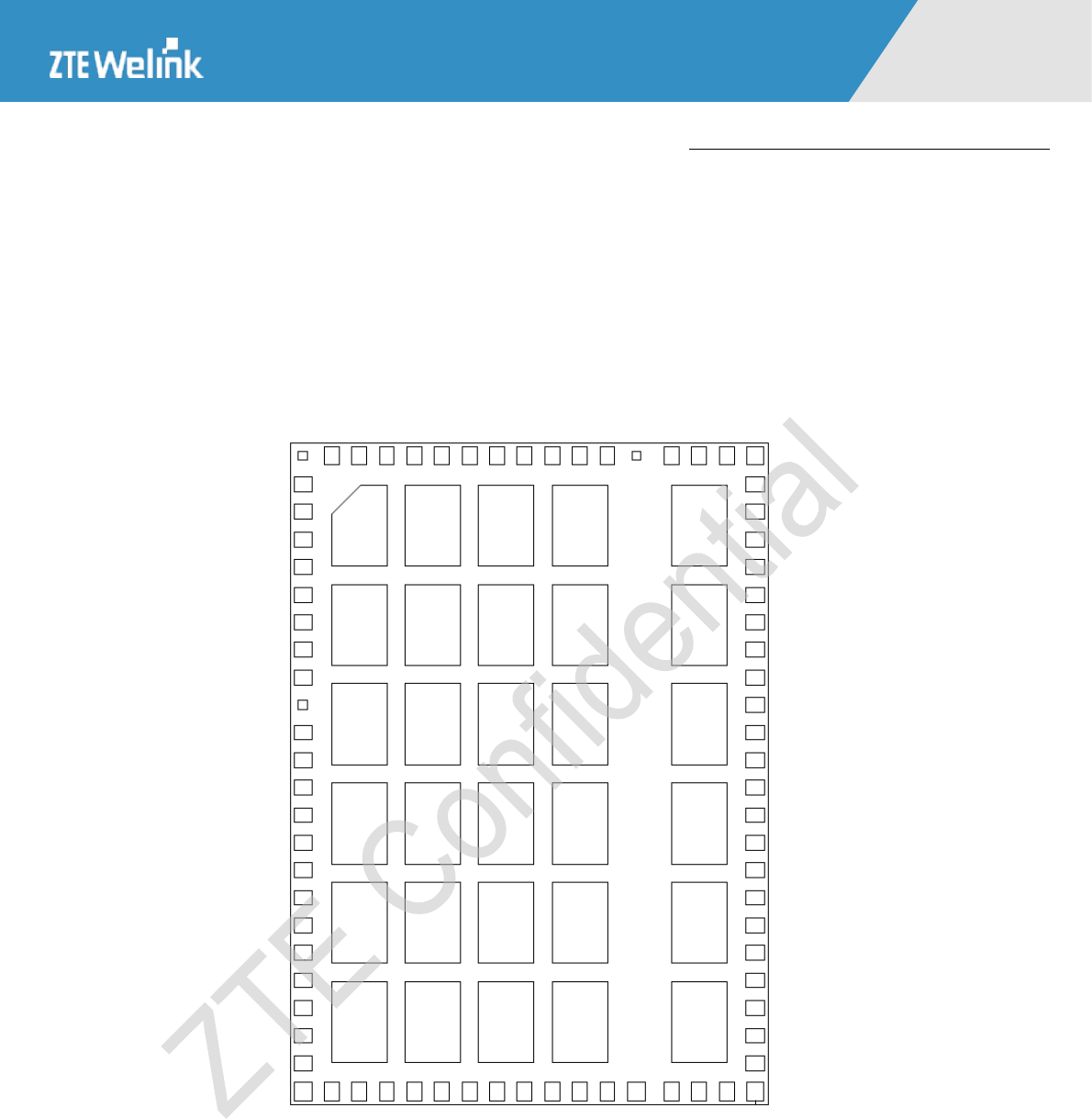
MF206A is a 108-pin LGA encapsulation module. Except for the signal PIN, there are many dedicated
heat-dissipation ground wielding panel to improve the grounding performance, mechanical strength and
heat-dissipation performance. There are altogether 30 heat-dissipation ground wielding panels, evenly
distributed at the bottom of PCB. The dimensions of 108-pin LGA encapsulation are 26*36mm, and the height is
2.5+/-0.2mm. The location of PIN 1 is identified by the ground wielding panel with an inclination at the bottom,
and its angle orientates to the top welding panel of the corresponding module. Figure 2–2 is a figure about the
dimensions of module, and the unit of dimensions is mm.
Figure 2–2 Module Dimensions
Hardware Development Guide of Module Product
All Rights reserved, No Spreading abroad without Permission of ZTEWelink 17
MF206A
(Top View)
2.2 Technical Parameters
The major features of module can be described from the aspects of mechanic feature, base band, radio frequency,
technical standard and environment feature. Table 2-1 is a list of the major technical parameters and features
supported by module.

Hardware Development Guide of Module Product
All Rights reserved, No Spreading abroad without Permission of ZTEWelink 18
MF206A
Table 2–1 Major Technical Parameters
Name
Item
Specifications
Mechanical
Feature
Dimensions
36mm * 26mm * (2.5+/-0.2)mm
Weight
About 5.5g
Encapsulation type
LGA package(108 Pin)
Baseband
Processor architecture
ARM 9 architecture
(U)SIM/SIM
Standard 6 PIN SIM card interface
Support 3V SIM card and 1.8V SIM card
Memory
32MByte NAND Flash/128MByte DDR
USB interface
USB 2.0 HIGH SPEED, the data transfer rate can reach up to 480
Mbps.
Can be used for AT command communication, data transmission,
GNSS NMEA output, software debug and firmware upgrade
UART interface
Used for AT command, data transmission or Diag service
And can be switch by the command of +UART
Maximum power
consumption
2.2W note1
Power Supply
The range of voltage supply is 3. 4V-4.2V, and the typical value
is3.8V
Working current note2
Peak current
≤2A (3.8V)
Average normal working current
≤500mA (3.8V)
Average normal working current
(without services)
≤75mA
Standby current
≤5mA (3.8V)
RF
GSM band
EDGE/GPRS/GSM Quad-band: GSM850, EGSM900, DCS1800,
PCS1900.
UMTS band
UMTS: 2100/1900/850(900)MHz
RxDiv band
NAnote3
Max. Transmitter Power
UMTS2100/1900/850(900): Power Class 3 (+24 +1/-3dBm)
GSM/GPRS 850MHz/900MHz: Power Class 4 (+33±2dBm)
GSM/GPRS 1800MHz/1900MHz: Power Class 1 (+30±2dBm)
EDGE 850MHz/900MHz: Power Class E2 (+27±3dBm)
EDGE 1800MHz/1900MHz: Power Class E2 (+26 -4/+3dBm)
Receiving sensitivity
WCDMA2100: ≤-106.7dBm
WCDMA1900/850: ≤-104.7dBm

Hardware Development Guide of Module Product
All Rights reserved, No Spreading abroad without Permission of ZTEWelink 19
MF206A
Name
Item
Specifications
WCDMA900: ≤-103.7dBm
GSM850/900/1800/1900: ≤-102dBm
Main antenna interface
Support
Receive diversity (GPS)
antenna interface
Support the GPS wielding panel interface, don’t support the diversity
antenna interface .We don’t provide the antenna, and the antenna is
provided by the third party.
Technical
Standard
Data rate
GSM CS: UL 9.6kbps/DL 9.6kbps
GPRS: Multi-slot Class 10
EDGE: Multi-slot Class 12
WCDMA CS: UL 64kbps/DL 64kbps
WCDMA PS: UL 384kbps/DL 384kbps
HSDPA: DL 3.6Mbps
GPRS type
Class B
3GPP protocol
R99,R5
Other protocols
Support embedded TCP /UDP protocols
Support PPP protocol
Support the protocols PAP (Password Authentication Protocol) and
CHAP (Challenge Handshake Authentication Protocol) usually used
for PPP connections.
Operating system
Windows XP (SP2 and later)
Windows Vista
Windows 7
WinCE5.0/6.0 (X86 and ARM)
Linux
Android 2.x / 4.x
Environment
Feature note4
Normal Working
Temperature
-30 to 75° C
Storage Temperature
-45 to 90° C
Humidity
5%~ 95%
Application
RAS dialup
Support
GPS/AGPS
Support
SMS
Support Text and PDU mode.
Point to point MO and MT.
SMS Status Report & SMS centre address setting

Hardware Development Guide of Module Product
All Rights reserved, No Spreading abroad without Permission of ZTEWelink 20
MF206A
Name
Item
Specifications
Management of SMS: read, write, send, receive, delete, storage
status, SMS list, new SMS alert
Network locking
Support
SIM READER
Support
AT Commands
Compliant with 3GPP TS 27.007, 27.005 and ZTEWelink AT
commands.
Upgrading
Support, the time of upgrading is less than 12min.
NOTE:
1: Test condition: The maximum power consumption of the module refers to the average value measured
under the maximum transmission power;
2: In the working current, the peak current, average normal working current, average normal working
current (without services) are all the maximum value measured under the maximum power consumption.
The standby current refers to the current under the SLEEP mode
3: NA means unrelated.
4: Using the module beyond these conditions may result in permanent damage to the module.
2.3 Function Overview
2.3.1 Baseband Function
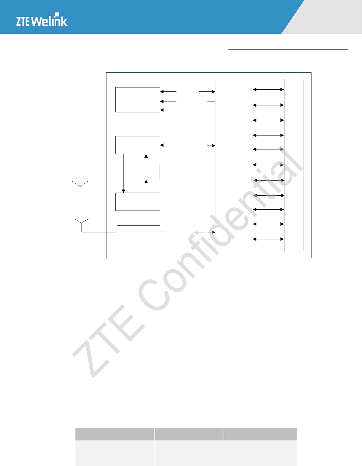
The baseband part of module mainly includes the following signal groups: USB signal, (U)SIM card signal,
wakeup signal, working status indicator signal, UART signal, SD interface signal, I2C interface signal, module
power-on/resetting signal, SPI, main antenna interface, GPS antenna interface and power-supply interface.
Figure 2–3 is a diagram of the system connection structure.
Hardware Development Guide of Module Product
All Rights reserved, No Spreading abroad without Permission of ZTEWelink 21
MF206A
Figure 2–3 System Connection Structure
PA and
Switch
RF
Baseband
Memory
108 Pin LGA Connector Interface
USB
USIM
UART
I2C
SD
SPI
LED
POWER
JTAG
RESET
Data Bus
Address Bus
Control
Communication
Tx SAW
Filter
Main Antenna
Filter
RX
GPS Antenna
Rx
ADC
2.3.2 Radio Frequency Function
The radio frequency function of module can be viewed from the aspect of over-the-air wireless bearer network,
frequency band, whether the receive diversity feature is supported, and the GPS function.
1. Support UMTS 850(900)/1900/2100MHz;
2. Support GSM/EDGE/GPRS 850/900/1800/1900 MHz;
3. Support GPS/AGPS;
The working frequency band of module is as shown in Table 2–2.
Table 2–2 Working Frequency Band
Working Frequency Band
Uplink Frequency Band
Downlink Frequency Band
UMTS850
824 MHz — 849 MHz
869 MHz — 894 MHz
UMTS900
880 MHz — 915 MHz
925 MHz — 960 MHz

Hardware Development Guide of Module Product
All Rights reserved, No Spreading abroad without Permission of ZTEWelink 22
MF206A
UMTS1900
1850 MHz — 1910 MHz
1930 MHz — 1990 MHz
UMTS2100
1920 MHz — 1980 MHz
2110 MHz — 2170 MHz
GSM850
824 MHz — 849MHz
869 MHz — 894 MHz
GSM900
890 MHz — 915MHz
935 MHz — 960MHz
GSM1800
1710 MHz — 1785MHz
1805 MHz — 1880MHz
GSM1900
1850 MHz — 1910MHz
1930 MHz — 1990MHz
Hardware Development Guide of Module Product
All Rights reserved, No Spreading abroad without Permission of ZTEWelink 23
MF206A
3 Interfaces
3.1 Definition of PINs
3.1.1 Definition of PIN I/O Parameters
The definition of module I/O parameter is as shown in Table 3–1.
Table 3–1 PIN Parameters
PIN Attribute
Description
DI
Digital Input Pin
DO
Digital Output Pin
AI
Analog Input Pin
AO
Analog Output Pin
B
Two-way digital port, CMOS
input
Z
High-resistance output
P1
PIN group 1, the power supply
voltage is VDD_P1
P2
PIN group 2, the power supply
voltage is VDD_P2
PU
PIN internal pull-up
PD
PIN internal pull-down
3.1.2 PIN Configuration Diagram
The PIN sequence of interfaces on module is defined as shown in Figure 3–1.
Hardware Development Guide of Module Product
All Rights reserved, No Spreading abroad without Permission of ZTEWelink 24
MF206A
Figure 3–1 PIN Configuration Diagram
2 3 45 6 7 8 9 10 11 12 14 15 16 17
18
19
20
21
22
23
24
25
26
27
28
29
30
31
32
33
34
35
36
37
38
39
40
41424344454647484950
51
5253545556
57
58
59
60
61
62
63
64
65
66
67
68
69
70
71
72
73
74
75
76
77
78
79 80 81 82 83
84 85 86 87 88
89 90 91 92 93
94 95 96 97 98
99 100 101 102 103
104 105 106 107 108
13
1
ANT_MAIN
GND
JTAG_RESOUT_N
PON_RST_N
POWER_ON
AP_READY
I2C_SCL
I2C_SDA
MODULE_READY
AP_WAKEUP_MODULE
MODULE _WAKEUP_AP
GND
NC
GND
NC
NC
NCSPI_CLK
NC
MODULE_POWERON
LED_GREEN
LED_RED
LED_BLUE
VPH_PWR
VPH_PWR
VPH_PWR
VPH_PWR
UART_CTS
UART_RFR
UART_TXD
UART_RXD
GND
NC
NC
NC
NC
GND
ADC
GND
SPI_CS_N
SPI_DATA_MI_SO
SPI_DATA_MO_SI
USB_VBUS
GND
USB_DP
USB_DM
GND
VREG_RUIM
UIM_DATA
UIM_CLK
UIM_RST
UIM_DP
UIM_DM
GND
VREG_SDCC
SDCC_CMD
SDCC_CLK
SDCC_DATA3
SDCC_DATA2
SDCC_DATA1
SDCC_DATA0
SD_DET_N
GND
NC
NC
GND
NC
NC
GND
GPS_ANT
GND
JTAG_TRST_N
JTAG_RTCK
JTAG_TCK
JTAG_TDO
JTAG_TDI
JTAG_TMS
GND
(Top View)

Hardware Development Guide of Module Product
All Rights reserved, No Spreading abroad without Permission of ZTEWelink 25
MF206A
3.1.3 PIN Description
Table 3–2 PIN Interface Definition
PIN
Signal Definition
Voltage
I/O
PIN Attribute
PU/PD
Remark
1
ANT_MAIN
--
AI/
AO
Main antenna feedback
point(50 ohm)
--
2
GND
--
--
Ground
--
3
JTAG_RESOUT_N
P1
DI
JTAG reset LGA
module
--
4
PON_RST_N
P1
DI
Reset the module
--
Pull-up to 1.8V internally.
Active low.
5
POWER_ON
P1
DI
Turn on/off the
module.
PU
Pull-up to 1.8V internally.
6
AP_READY
P1
DI
Module queries AP
sleep status
--
7
I2C_SCL
P1
B
I2C serial clock
--
8
I2C_SDA
P1
B
I2C serial data
--
9
MODULE_READY
P1
DO
AP queries Module
sleep status
--
10
AP_WAKEUP_MOD
ULE
P1
DI
AP wakes up Module
--
Low-power level wakeup.
To make the module
standby, the AP needs to
raise up this low signal.
11
MODULE
_WAKEUP_AP
P1
DO
Module wakes up AP
--
12
GND
--
--
--
--
13
NC
--
--
--
--
--
14
GND
--
--
--
--
15
NC
--
--
--
--
--
16
NC
--
--
--
--
--
17
NC
--
--
--
--
--
18
NC
--
--
--
--
--
19
MODULE_POWER
ON
P1
DO
MODULE power-on
status indicator
--
20
LED_GREEN
P1
AO
Signal indicator
interface
--
high-current driver.

Hardware Development Guide of Module Product
All Rights reserved, No Spreading abroad without Permission of ZTEWelink 26
MF206A
PIN
Signal Definition
Voltage
I/O
PIN Attribute
PU/PD
Remark
21
LED_RED
P1
AO
Signal indicator
interface
--
high-current driver.
22
LED_BLUE
P1
AO
Signal indicator
interface
--
high-current driver.
23
VPH_PWR
Vmax =
4.2V
Vmin =
3.4V
Vnorm =
3.8V
AI
Power supply
--
It must be able to provide
sufficient current in a
transmitting burst which
typically rises to 2.0A.
24
VPH_PWR
--
25
VPH_PWR
--
26
VPH_PWR
--
27
UART_CTS
P1
DI(
HV
)
UART clear to send
signal
--
--
28
UART_RFR
P1
DO
UART ready for
receive signal
--
--
29
UART_TXD
P1
DO
UART transmit data
output
--
--
30
UART_RXD
P1
DI
UART receive data
input
--
--
31
GND
--
--
Ground
--
--
32
NC
--
--
--
--
--
33
NC
--
--
--
--
--
34
NC
--
--
--
--
--
35
NC
--
--
--
--
--
36
GND
--
--
Ground
--
--
37
ADC
--
AI
Analog / Digital
converter input
--
--
38
GND
--
--
Ground
--
--
39
SPI_CS_N
P1
DO
SPI interface channel
signal
--
--
40
SPI_CLK
P1
DO
SPI clock signal
--
--
41
SPI_DATA_MI_SO
P1
B
SPI data IO signal
--
--
42
SPI_DATA_MO_SI
P1
B
SPI data IO signal
--
--
43
USB_VBUS
--
AI
Power sense for the
internal USB
--
Pay attention to the
power-on sequence of

Hardware Development Guide of Module Product
All Rights reserved, No Spreading abroad without Permission of ZTEWelink 27
MF206A
PIN
Signal Definition
Voltage
I/O
PIN Attribute
PU/PD
Remark
transceiver
VPH_PWR
44
GND
--
--
Ground
--
--
45
USB_DP
--
AI/
AO
USB differential data
(+)
--
Require differential
impedance of 90Ω.
46
USB_DM
--
AI/
AO
USB differential data
(-)
--
Require differential
impedance of 90Ω.
47
GND
--
--
Ground
--
--
48
VREG_RUIM
P1/ P2
AO
Power supply for
USIM card.
--
--
49
UIM_DATA
P1/ P2
B
Data signal of USIM
card.
--
--
50
UIM_CLK
P1/ P2
DO
Clock signal of USIM
card.
--
--
51
UIM_RST
P1/ P2
DO
Reset signal of
USIM card.
--
--
52
UIM_DP
P1/ P2
AI/
AO
Data plus line
--
--
53
UIM_DM
P1/ P2
AI/
AO
Data minus line
--
--
54
GND
--
--
Ground
--
--
55
VREG_SDCC
P2
AO
Power supply for SD
card.
--
--
56
SDCC_CMD
P2
B
SD card control signal
HV
--
57
SDCC_CLK
P2
DO
SD card clock signal
--
--
58
SDCC_DATA3
P2
B
SD card data signal
--
--
59
SDCC_DATA2
P2
B
SD card data signal
--
--
60
SDCC_DATA1
P2
B
SD card data signal
--
--
61
SDCC_DATA0
P2
B
SD card data signal
--
--
62
SD_DET_N
--
--
NC
--
Reserved
63
GND
--
--
Ground
--
--
64
NC
--
--
--
--
--
65
NC
--
--
--
--
--
66
GND
--
--
Ground
--
--
67
NC
--
--
--
--
--
Hardware Development Guide of Module Product
All Rights reserved, No Spreading abroad without Permission of ZTEWelink 28
MF206A
PIN
Signal Definition
Voltage
I/O
PIN Attribute
PU/PD
Remark
68
NC
--
--
--
--
--
69
GND
--
--
Ground
--
--
70
GPS_ANT
--
--
GPS antenna
--
--
71
GND
--
--
Ground
--
--
72
JTAG_TRST_N
P1
DI
JTAG reset
PD
--
73
JTAG_RTCK
P1
DO
JTAG return clock
--
--
74
JTAG_TCK
P1
DI
JTAG clock input
-PU
--
75
JTAG_TDO
P1
Z
JTAG test data output
--
--
76
JTAG_TDI
P1
DI
JTAG test data input
PU
--
77
JTAG_TMS
P1
DI
JTAG test mode select
PU
--
78
GND
--
--
Ground
--
--
79.-
108.
GND
--
--
Heat-dissipation welder
--
--
NOTE:
―NC‖ indicates Not Connected internal. That is, there is no connection inside the module. P1 and P2
refer to the power-supply signal level group 1 and 2.
If not used, almost all pins should be left disconnected. The only exceptions are the following pins as
shown in the Table 3-3 below:
Table 3–3 Mandatory Pins of Module
PIN
Signal Definition
Remark
1
ANT_MAIN
5
POWER_ON
Pull-up to 1.8V internally.
23
VPH_PWR
It must be able to provide sufficient current in a
transmitting burst which typically rises to 2.0A.
43
USB_VBUS
45
USB_DP
Require differential impedance of 90Ω.
46
USB_DM
Require differential impedance of 90Ω.
48
VREG_RUIM
49
UIM_DATA

Hardware Development Guide of Module Product
All Rights reserved, No Spreading abroad without Permission of ZTEWelink 29
MF206A
50
UIM_CLK
51
UIM_RST
2/12/14/31/36/
38/44/47/54/63
/66/69/71/78
GND
79.-108.
GND
3.2 Working Condition
Table 3–4 Working Condition
Signal
Description
Min
Typical
Max
Unit
VPH_PWR
Main power supply of the module
3.4
3.8
4.2
V
USB_VBUS
Power supply PIN of USB PHY
3.3
5
5.25
V
ADC
Analog input
0
--
2.2
V
VDD_P1
Voltage of PIN group P1
1.65
1.8
1.95
V
VDD_P2
Voltage of PIN group P2
2.7
2.85
3
V
NOTE:
1. The typical voltage refers to the default I/O voltage of P1 and P2 PIN group. It is required that the
external input PIN provides this voltage.
2. The voltage design of external circuit interfaces should match that of the module PINs.
3. When VPH_PWR works within the voltage range, it can reach good whole-set performance. If it is
lower than the minimum value, the whole-set performance will be affected, or the module cannot work
normally. If it is higher than the maximum value, the module might be damaged

Hardware Development Guide of Module Product
All Rights reserved, No Spreading abroad without Permission of ZTEWelink 30
MF206A
3.3 Feature of Digital Power Level
Table 3–5 Power Level Range of Digital Signal
Parameter
Description
Min
Max
Unit
VIH
High level of input voltage
0.65*VDD_PX
VDD_PX+0.3
V
VIL
Low level of input voltage
-0.3
0.35* VDD_PX
V
VOH
High level of output voltage
VDD_PX-0.45
VDD_PX
V
VOL
Low level of output voltage
0
0.45
V
3.4 Power Interface
3.4.1 Description of Power PINs
Power VPH_PWR signal (PIN No: 23-26). This is the positive signal of 3.8V power supply.
GND signal (PIN No: 2/12/14/31/36/38/44/47/54/63/66/69/71/78). This is the power ground and signal ground
of module, which needs to be connected to the ground on the system board. If the GND signal is not connected
completely, the performance of module will be affected. Besides, there are altogether 30 heat-dissipation
wielding panel with PIN No. 79-108.
3.4.2 Requirement of Power Supply
The power supply is recommended to be within the range of 3.4~4.2V. If the network is in poor situation, the
antenna will transmit at the maximum power, and the transient maximum peak current under 2G mode can reach
as high as 2A. So the power supply capacity for peak current needs to be above 2.5A, and the average current
needs to be above 2A.
NOTE:
More details about the designing of power supply please refer to Chapter 4 of Power Interface Design
Guideline of this document.

Hardware Development Guide of Module Product
All Rights reserved, No Spreading abroad without Permission of ZTEWelink 31
MF206A
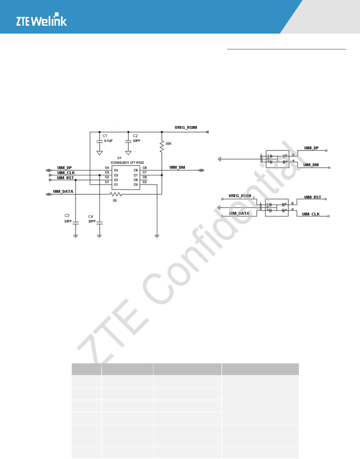
3.5 (U)SIM Card Interface
3.5.1 Description of PINs
Module baseband processor integrates the (U)SIM card interface in compliance with ISO 7816-3 standards, and
supports to automatically detect 3.0V/1.8V (U)SIM cards. The signals on SIM card interface is as shown in
Table 3-6.;
Table 3–6 Definition & Description of (U)SIM Card Signal Group
PIN No.
Pin Name
Signal Definition
Signal Description
48
VREG_RSIM
Power supply for USIM card.
Output range: 1.5-3.0V
49
UIM_RST
Reset signal of USIM card.
UIM card reset signal, output
from the module
50
UIM_DATA
Data signal of USIM card.
--
51
UIM_CLK
Clock signal of USIM card.
--
52
UIM_DP
Data cable
USIM card data signal, applied
on a large-capacity SIM card
53
UIM_DM
Data cable
USIM card data signal, applied
on a large-capacity SIM card
3.5.2 Electric Feature
On the line close to the (U)SIM card console, be sure to add the ESD circuit protection during the design.
To comply with the requirements of 3GPP TS 51.010-1 and EMC authentication, it is recommended to place
(U)SIM card console close to the (U)SIM card interface, to prevent the wiring from being too long, which might
seriously distort the waveform and thus affect the signal integrity. It is recommended to make the grounding
protection for UIM_CLK and UIM_DATA signal wiring. Cascade one 0.1μF and 33pF capacitor between
VREG_RSIM and GND, and cascade a 33pF capacitor between UIM_CLK, UIM_RST and GND, to filter out
the interference by RF signals. It is recommended to cascade a 20ohm resistance on UIM_DATA cable.
Hardware Development Guide of Module Product
All Rights reserved, No Spreading abroad without Permission of ZTEWelink 32
MF206A
3.5.3 Application of (U)SIM Card Interface
The following Figure 3-2 shows the reference design of the USIM card.
Figure 3–2 (U)SIM Card Signal Connection Circuit
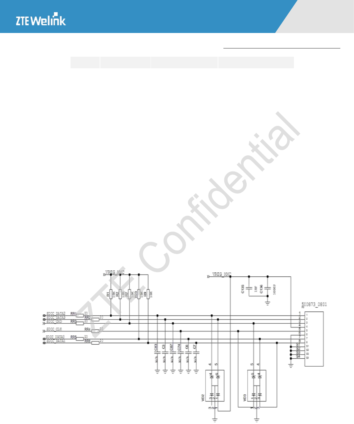
3.6 SD Card Interface
3.6.1 Description of PINs
The SD card interface of module is the storage card based on FLASH, embedded with 4-bit and 1-bit SD
controller, supporting SD and Mini SD cards. Its PIN signals are as shown in Table 3-7.
Table 3–7 Definition of SD Card Signal Interface
PIN No.
Pin Name
Signal Definition
Signal Description
61
SDCC_DATA0
SD card data cable PIN
SD card data cable
60
SDCC_DATA1
SD card data cable PIN
59
SDCC_DATA2
SD card data cable PIN
58
SDCC_DATA3
SD card data cable PIN
57
SDCC_CLK
SD card clock cable PIN
SD control clock output can
reach up to 20MHz
56
SDCC_CMD
SD card control PIN
--
Hardware Development Guide of Module Product
All Rights reserved, No Spreading abroad without Permission of ZTEWelink 33
MF206A
55
VREG_MMC
SD card power
3V
3.6.2 Electric Feature
SDCC_CLK: Clock signal, host2device, default is 0~25MHz.
SDCC_CMD: Command/response, two-way: the command can be sent from the host to a single card/all cards,
the response is sent from a single card/all cards to the host.
SDCC_DATA[3..0]: Data cable, two-way, default is 0~12.5MB/sec.
3.6.3 Application of SD Card Interface
Figure 3–3 is the reference design diagram for the SD interface. The detection of SD card adopts the polling
mode of DATA3 signal cable to judge whether T card is inserted or not.
Figure 3–3 SD Typical Application Circuit

Hardware Development Guide of Module Product
All Rights reserved, No Spreading abroad without Permission of ZTEWelink 34
MF206A
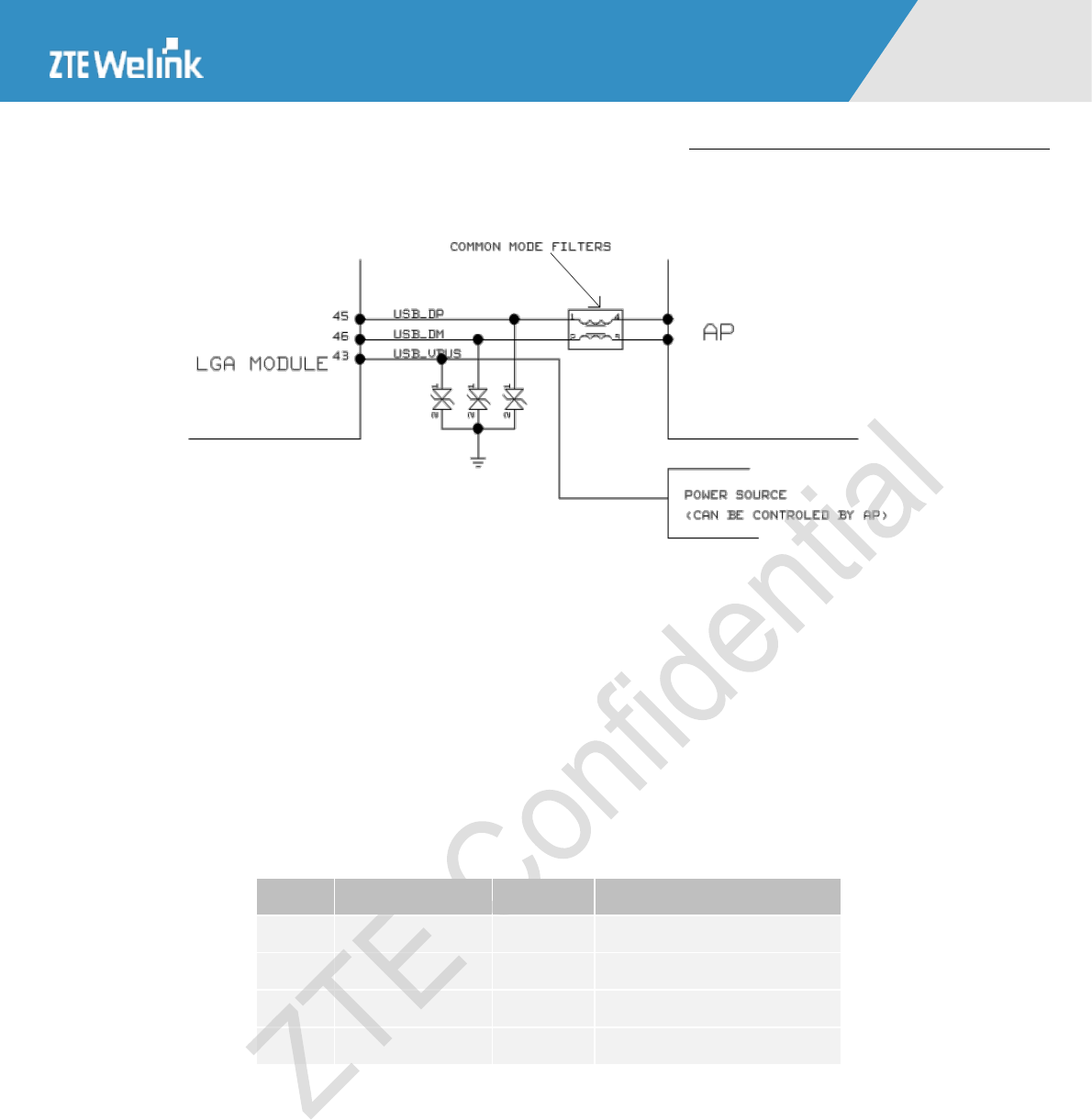
3.7 USB2.0 Interface
3.7.1 Description of PINs
MF206A has the high-speed USB2.0 interface, which supports both the full-speed mode and the high-speed
mode. The main processor (AP) is connected with the module via the USB interface to transmit data.
3.7.2 Electric Feature
The USB interface complies with the USB2.0 specifications and the electric features. USB_DP, USB_DM are
wired strictly according to the differential mode, and the length difference between the two cables should be
restricted within 1mm.
NOTE:
NOTE: If the users of module need the wakeup and sleep function, and your AP side connects with the
module through USB interface, the AP side needs to support USB suspend and resume to realize this
function.
The differential impedance should be controlled within 90ohm.
It is recommended to connect to a high-speed common-mode echo filter on the USB differential signal wire. If
the cable is exposed to the external environment, it is suggested to add an ESD protection device. The power
capacity of the ESD protection device should be kept within 1.5pF.
3.7.3 Application of USB Interface
The USB bus is mainly used in data transmission, software upgrading and modular program detection. Figure
3–4 shows a reference circuit design.
Hardware Development Guide of Module Product
All Rights reserved, No Spreading abroad without Permission of ZTEWelink 35
MF206A
Figure 3–4 USB Typical Circuit Application
3.8 SPI (Serial Peripheral Interface) Bus Interface
3.8.1 Description of PINs
The definition of SPI interface signaling is defined as shown in Table 3-8.
Table 3–8 Definition of SPI Signal
PIN No.
Pin Name
I/O Type
Signal Description
39
SPI_ CS_N
O
SPI segment
40
SPI_ CLK
O
SPI clock
41
SPI_MISO_DATA
B
Main input, slave output
42
SPI_MOSI_DATA
B
Main input, slave output
3.8.2 Electric Feature
The SPI bus is configured as the master equipment, and there are three modes for SPI:
Running mode: Basic running mode.
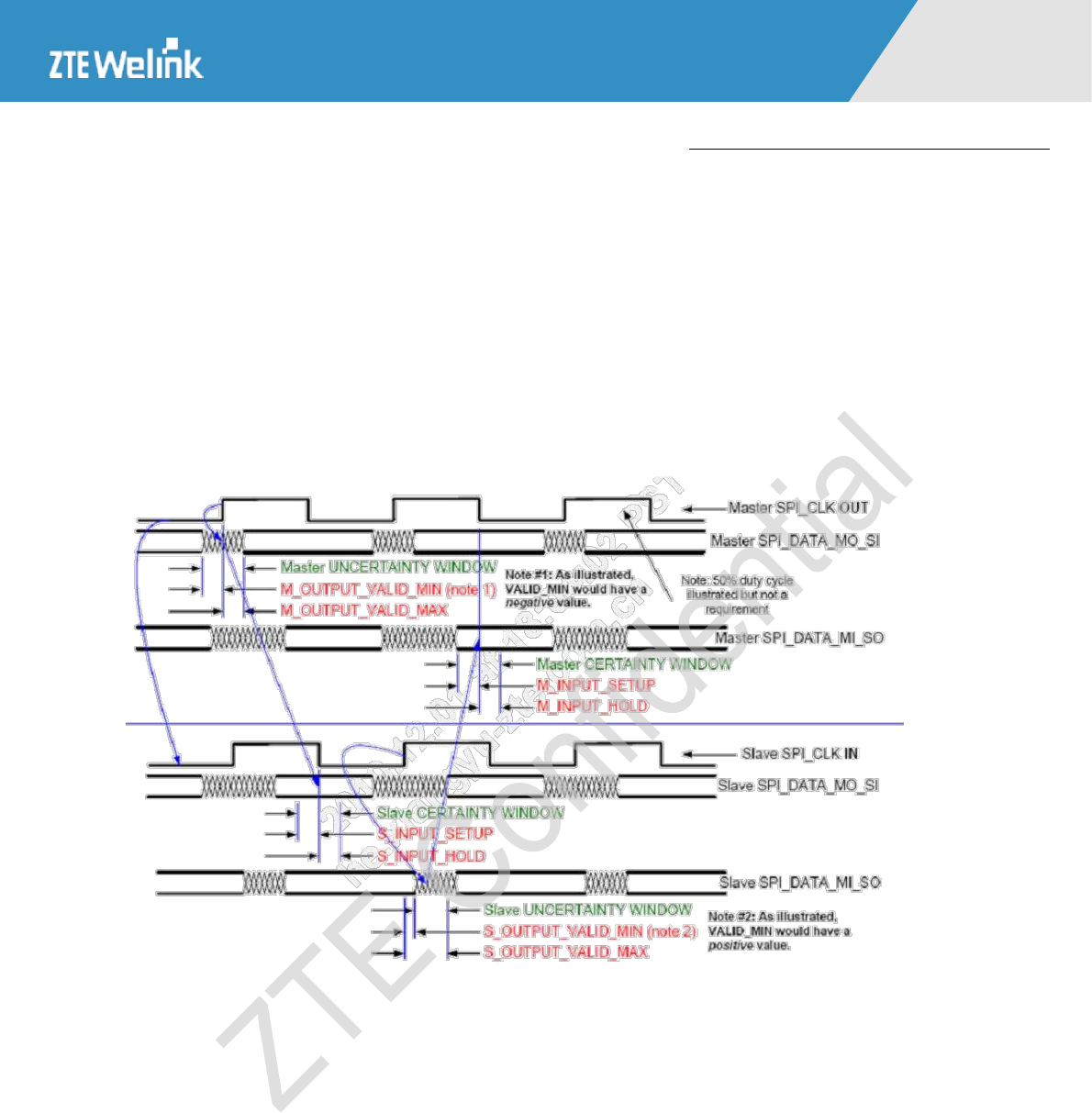
Hardware Development Guide of Module Product
All Rights reserved, No Spreading abroad without Permission of ZTEWelink 36
MF206A
Waiting mode: The waiting mode of SPI is a configurable low-power mode, enabled by the byte of the control
registered. In the waiting mode, if the waiting byte is cleared, SPI works under the similar running mode.
However, if SPI waits for the position byte, SPI clock stops and enters the low-power status.
Stop mode: Under the stop mode, SPI is not available, so the power consumption is reduced. If SPI is configured
as the master equipment, any transmission process will be stopped, but it can enter the running mode when the
waiting mode stops. Figure 3–5 is the SPI bus sequence chart.
Figure 3–5 SPI Bus Sequence Chart
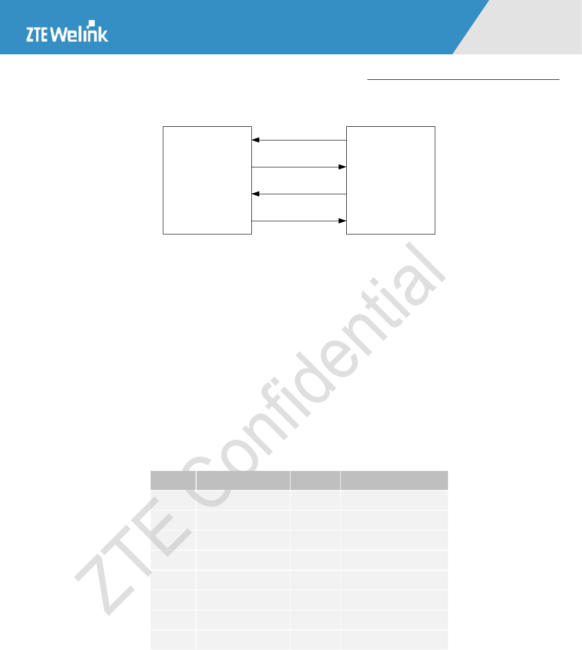
3.9 I2C Bus
3.9.1 Description of PINs
I2C is the two-wire bus for the communication between ICs, which supports any IC process (NMOS, CMOS,
dual-polarity). The two signal wires, serial data (SDA) and serial clock (SCL), can transmit information between
the connected equipment. Each equipment is identified by the unique address (such as the micro controller,
storage, LCD driver, audio DAC or keyboard interface). Due to the different functions of the equipment, it can
be used as both the sender and the receiver.
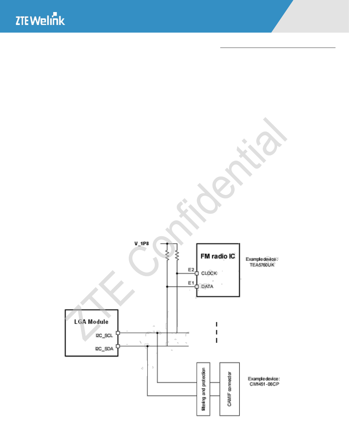
Hardware Development Guide of Module Product
All Rights reserved, No Spreading abroad without Permission of ZTEWelink 37
MF206A
3.9.2 Electric Feature
The I2C interface has the following features:
1. The two-wire bus is used for the communication between ICs.
2. It supports any external equipment of any manufacturing technology (1.8V).
3. It supports the external functions, such as the image sensor, micro controller, FM radio chip, LCD
chip, audio DAC and keyboard interface.
The I2C interface has two working modes with different transmission ratios: standard mode with a speed as high
as 100kbps; high-speed mode with a speed as high as 400kbps. Figure 3–6 is the I2C reference circuit design
diagram.
Figure 3–6 I2C Reference Circuit Diagram

Hardware Development Guide of Module Product
All Rights reserved, No Spreading abroad without Permission of ZTEWelink 38
MF206A
3.10 UART Interface
3.10.1 Description of PINs
Module provides a circuit of serial communication interface UART, which complies with the RS-232 interface
protocol, and supports the 4-wires serial bus interface or 2-wires serial interface. Via the UART interface, the
module can perform the serial communication and AT instruction interaction with the external.
This UART port supports the programmable data width, programmable data stop digit and programmable
odd/even checksum, and has an independent TX and RX FIFOs (512 bytes for each). For the normal UART
application (non-Bluetooth), the maximum baud rate is 230400bps, the 4Mbps high baud rate is only used on
Bluetooth 2.0 application, and the default baud rate is 115200bps. The PINs are defined as shown in Table 3-9.
Table 3–9 Definition of UART Signal
PIN No.
Pin Name
Signal Definition
Signal Description
27
UART1_CTS
UART clear to send signal
UART power level
is 1.8V.
28
UART1_RFR
UART ready for receive signal
29
UART1_TXD
UART transmit data output
30
UART1_RXD
UART receive data input
NOTE:
If the users of module need the wakeup and sleep function, and you AP side connects with the module
through UART interface, you need to connect the PIN10&PIN11 (AP_WAKEUP_MODULE,
MODULE_WAKEUP_AP) to the AP side to realize this function. The details of this two pin you can refer
to chapter 3.13.
3.10.2 Electric Feature
During the software interconnection process, there is a method of capturing logs, and it is recommended that this
interface be kept during the design and the testing point be reserved. If the module is used together with the
application processor, and the PWL matches with 1.8V, the 4-wires connection mode is as shown in Figure 3–7.
The 4-wires or 2-wires mode can be used for connection. The module interface PWL is 1.8V. If it does not
match the PWL of AP interface, it is recommended to add the PWL conversion circuit.
Hardware Development Guide of Module Product
All Rights reserved, No Spreading abroad without Permission of ZTEWelink 39
MF206A
Figure 3–7 Module Serial Port & AP Application Processor
MF206A AP
RXD
RXDTXD
TXD
CTS
RFR CTS
RFR
3.11 JTAG (Joint Test Action Group) Interface
3.11.1 Description of PINs
The JTAG interface complies with the ANSI/ICEEE Std. 1149.1-1990 standard, and the interface is defined as
shown in Table 3-10.
Table 3–10 Definition of JTAG Signal
PIN No.
Pin Name
I/O Type
Signal Description
3
JTAG_RESOUT_N
DI
LGA reset
72
JTAG_TRST_N
DI-PD
JTAG reset
73
JTAG_RTCK
DO
JTAG return clock
74
JTAG_TCK
DI-PU
JTAG clock input
75
JTAG_TDO
Z
JTAG test data output
76
JTAG_TDI
DI-PU
JTAG test data input
77
JTAG_TMS
DI-PU
JTAG test mode select
78
GND
--
Grounding

Hardware Development Guide of Module Product
All Rights reserved, No Spreading abroad without Permission of ZTEWelink 40
MF206A
3.11.2 Application of JTAG Interface
On the system board, you need to reserve the testing point or interface of the related JTAG signal, so as to solve
the un-repairable fault of LGA module due to emergencies such as downloading interruption.
3.12 Power-on/Power-off & Reset Signal
3.12.1 Description of PINs
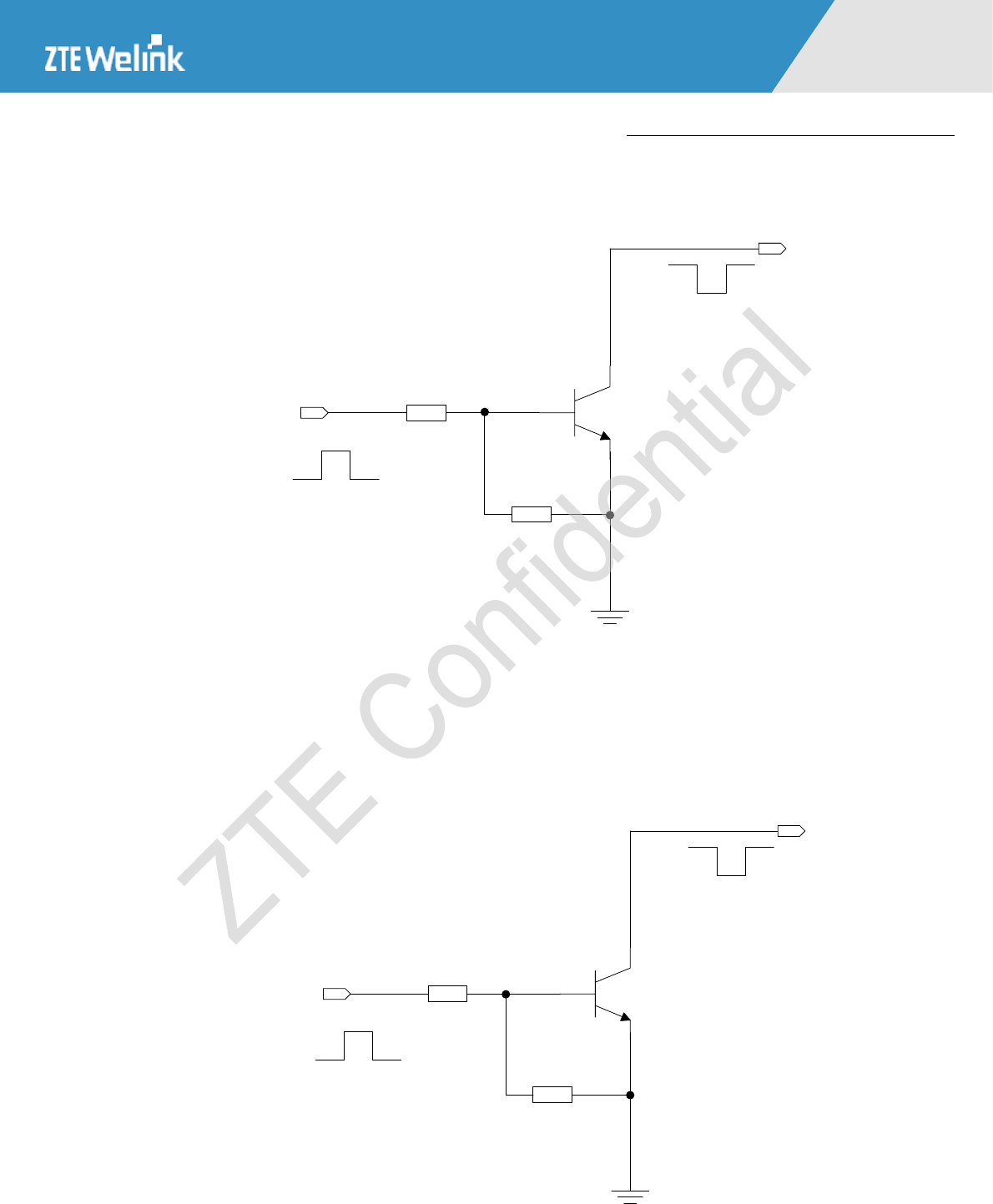
To turn on the module the pad POWER_ON must be tied low for at least 0.05 seconds and then released.
To turn off the module the pad POWER_ON must be tied low for at least 5 seconds and then released.
A simple circuit to do it is as shown in the following Figure 3-9.
NOTE:
The resistors R1 and R2 in Figure 3-9 and Figure 3-1 are only the recommended value and they may
different according to the users transistor selection.
Hardware Development Guide of Module Product
All Rights reserved, No Spreading abroad without Permission of ZTEWelink 41
MF206A
Figure 3–8 Turn on the Module Using Driving Circuit
≥50ms
Turn on pulse R2
R1
POWER_ON
You can reset the module by driving the PON_RST_N to a low level voltage for more than 100ms and then
releasing. A simple circuit to do it is as shown in the following Figure 3-10.
Figure 3–9 Resetting the Module Using Driving Circuit
≥100ms
Reset pulse R2
R1
PON_RST_N
Hardware Development Guide of Module Product
All Rights reserved, No Spreading abroad without Permission of ZTEWelink 42
MF206A
3.12.2 Power-on/Power-off Flow
To guarantee the user can power on and power off stably, you can refer to the power-on sequence chart as shown
in Figure 3-11 and the power-off sequence chart as shown in Figure 3-12. Table 3-11 shows the power-on and
resetting time, which needs to be paid attention to during the module power-on process.
1. Once VPH_PWR is powered on, the POWER_ON signal will be synchronized and be established
as the high PWL.
2. After VPH_PWR is established normally, the interval between it to the POWER_ON signal
cannot be too short. Refer to T2 parameter. ZTEWelink recommends that VPH_PWR adopt the
power-off plan that does not disconnect the power supply.
3. The power-on startup time takes the lower level of POWER_ON as the starting point, and
POWER_ON needs to be released after being kept on the low PWL for a period.
4. SUB_VBUS is the USB PHY power supply. It is not recommended to be established before
VPH_PWR.
During the process of establishing the module PINs, pay attention to the following items:
1. To power off by the POWER_ON signal, the T4 period needs to be designed as required.
2. After VPH_PWR and USB_VBUS are powered off, it is recommended not to disconnect the
power supply.
Figure 3–10 Power-on Sequence Chart of Module
VPH_PWR
USB_VBUS
POWER_ON
T1
T2
T3

Hardware Development Guide of Module Product
All Rights reserved, No Spreading abroad without Permission of ZTEWelink 43
MF206A
Figure 3–11 Power-off Sequence Chart of Module
POWER_ON
T5
T4
VPH_PWR
USB_VBUS
Table 3–11 Power-on/Power-off Time
Parameter
Description
Min
Typical
Max
Unit
T1
From powering on VPH_PWR to
establishing USB_VBUS
0
0.5
1
second
T2
From powering on VPH_PWR to Power-on
taking effect
1
1.5
--
second
T3
The period that the Power-on signal for
power on operation is kept on the low PWL
0.05
0.1
--
second
T4
The period that the Power-on signal for
power off operation is kept on the low PWL
4
5
--
second
T5
From the releasing the Power-on button for
power off operation to the power off of
VPH_PWR and USB_VBUS
1
2
--
second
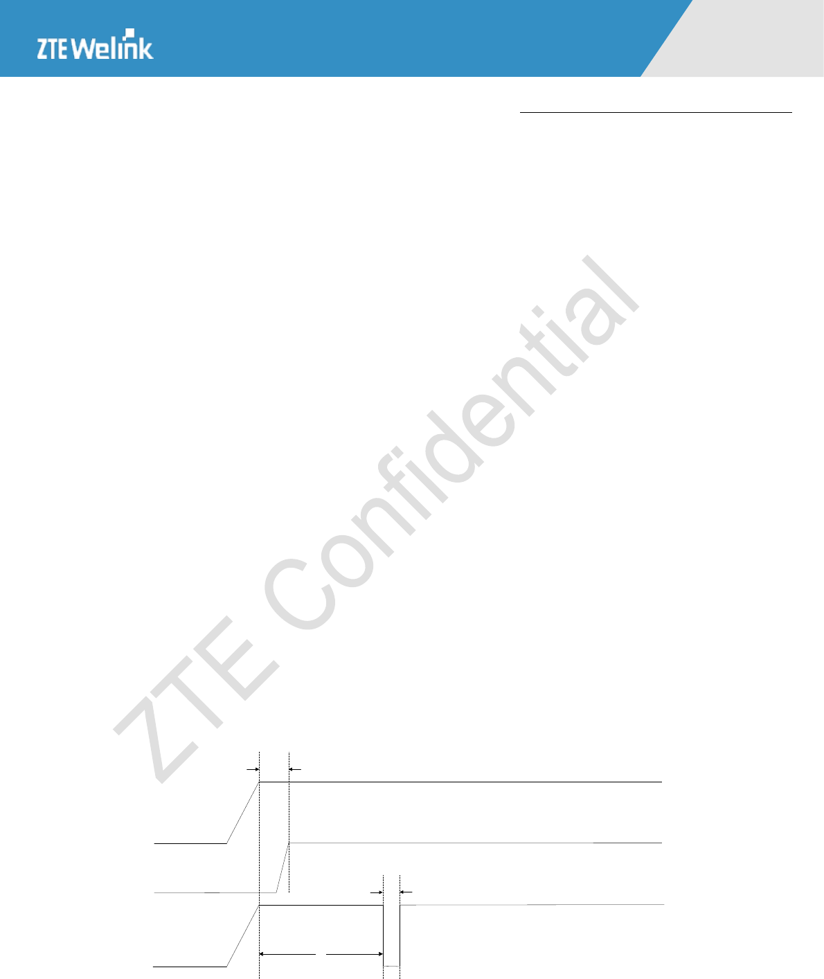
3.12.3 Resetting Flow
The PON_RST_N reset signal of module is the increasing resetting, so it is reset after decreasing this PIN by
100ms. Figure 3-13 is the module resetting flow. Figure 3-14 is the timing of resetting module.
Hardware Development Guide of Module Product
All Rights reserved, No Spreading abroad without Permission of ZTEWelink 44
MF206A
Figure 3–12 Module Resetting Flow
100ms
1
0
PON_RST_N
Figure 3–13 Timing of Resetting Module
VPH_PWR
PON_RST_N
Module
Status ResettingRunning Running
100ms
3.13 Interactive Application Interface
3.13.1 Description of PINs
Table 3-12 mainly describes the interfaces interacting with the application processor, including the following
three types of interfaces: querying, wakeup and status indication.
Table 3–12 Interactive Application Interface
PIN No.
Pin Name
I/O Type
Signal Description
6
AP_READY
DI
Module querying AP sleep status
9
MODULE_READY
DO
AP querying Module sleep status
10
AP_WAKEUP_MODULE
DI
AP wakeup Module
11
MODULE_WAKEUP_AP
DO
Module wakeup AP
19
MODULE_POWERON
DO
MODULE power-on status indication

Hardware Development Guide of Module Product
All Rights reserved, No Spreading abroad without Permission of ZTEWelink 45
MF206A
3.13.2 Interface Application
The module provides 5 handshake signals for the communication with the application processor (AP). By
MODULE_POWERON, AP can query whether LGA is powered on and is working normally. By
MODULE_READY, AP queries whether the LGA module has entered the sleep status, wakes up the module
under the sleep status by AP_WAKEUP _MODULE. In the same way, when AP is in the sleep status, the LGA
module can query the AP status by AP_READY, and wakes up AP by MODULE _WAKEUP_AP.
AP_READY: Indicates that the AP server is sleep: the high PWL indicates the sleep status, and the low PWL
indicates the wakeup status.
MODULE_READY: Indicates that the module is sleep: the high PWL indicates the sleep status, and the low
PWL indicates the wakeup status.
AP_WAKEUP_MODULE: After the module has entered the sleep status, the AP server can wake up the module
by the low PWL control; if it’s always on the low PWL, the module cannot enter the sleep status. After the AP
server enters the high PWL, the module enters the sleep status.
MODULE_WAKEUP_AP: After the AP server has entered the sleep status, the module can lower down this
signal to wake up the AP server. After the module has queried that the server sleep indicator AP_READY is low,
it resets this signal to high.
MODULE_POWERON: After the module is powered on, this signal is set to high, and kept until the system is
restarted or powered down. Low signal indicates that the server is not powered on, during the power-on process
or is being restarted.
3.14 LED Indicator Interface
3.14.1 Description of PINs
Table 3–13 Definition of LED PIN Signal
PIN
Signal Name
I/O Type
Function
20.
LED_GREEN
AO
Module signal indicator interface
21.
LED_RED
AO
Module signal indicator interface
22.
LED_BLUE
AO
Module signal indicator interface

Hardware Development Guide of Module Product
All Rights reserved, No Spreading abroad without Permission of ZTEWelink 46
MF206A
3.14.2 Interface Application
The LGA module has three PINs to control the LED indicator, which is used to indicate the network connection
status. The different modes of status indicator flashing indicate different network statuses. All the three PINs use
the current sink type of current source for control, which connects to the negative end of LED and connects to
VPH_PWR externally, to directly drive LED. Figure 3-16 is the reference circuit design diagram.
The flashing of indicator is controlled by the switch of RF, and the LED PIN indicates the control signal to the
external. The indicator status of network is as defined in Table 3-14. If the RF control is not needed, the AP
server can design the status of control indicator by itself.
Figure 3–14 Reference Circuit of Status Indicator
Table 3–14 Definition of Indicator Status
Indicator Status
Module Working Status
RED indicator always on
Not registered to the network
GREEN indicator always on
Have been registered to 2G network
GREEN indicator flashing
Have been registered to 2G network,
and there is data service as well.
BLUE indicator always on
Have been registered to 3G network
BLUE indicator flashing
Have been registered to 3G network,
and there is data service as well.

Hardware Development Guide of Module Product
All Rights reserved, No Spreading abroad without Permission of ZTEWelink 47
MF206A
4 Power Interface Design Guideline
This chapter provides the power supply requirements, general design rules and Power-on/Power-off/Reset flow
of modules. Users can design the power supply of module to achieve stable and well working performance
according to this document.
4.1 General Design Rules
When the ZTEWelink module is used for different external applications, pay special attention to the design for
the power supply.
In the process of peripheral circuit designing, users of this Module product should ensure that the external power
supply circuit is capable of providing sufficient power supply capacity firstly, and control the supply range
between 3.4V~4.2V strictly. If the value above module voltage range, it will lead the main chip burned, while
below module voltage range, it will affect the RF circuit’s work or cause shutdown and restart occurred. For the
design of high-speed USB signal lines, it requires to control the differential impedance at 90ohm. The voltage
design of external circuit interfaces should match that of the module PINs, and the detailed value can be got in
Table 3-2. The module product has a good RF indicator; customers can refer to the Chapter 5 of Antenna Design
Guide of Module Product in the process of antenna circuit designing. Otherwise it will affect the whole RF
performance.
4.2 Power Supply Requirement
The power supply of ZTEWelink LGA Type module is usually recommended to be within the range of 3.4~4.2V.
According to the requirement of mobile terminal device, the power supply voltage of module is 3.8V under
normal working condition.
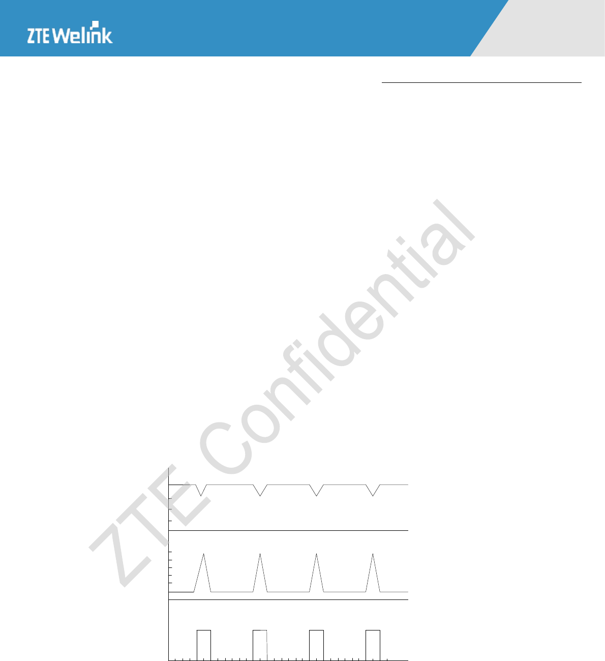
Hardware Development Guide of Module Product
All Rights reserved, No Spreading abroad without Permission of ZTEWelink 48
MF206A
In poor situation of the network, the antenna will transmit at the maximum power, and the transient maximum
peak current can reach as high as 2A. So the power supply capacity of system board needs to be above 2.5A to
satisfy the requirement of module peak current; and the average current on the system side needs to be above
2.0A. Meanwhile, consider the voltage drop of power supply on the side of main board. If the network is in a
poor situation or under 2G, the module peak current will be great, Therefore the power supply has to be designed
in order to withstand with these current peaks without big voltage drops; this means that both the electrical
design and the board layout must be designed for this current flow. If the layout of the PCB is not well designed
a strong noise floor is generated on the ground and the supply; and exceptions such as restart of the module may
occur.
The peak current of ZTEWelink module under the GSM BURST mode is different due to the differences in
actual network environments. And its transient current under different powers will be various as well. The
greater the power is, the greater the transient current is. The network quality also directly affects the work
current of the module. If the network is in well situation, the peak work current on the module will be small. But
if the network is in poor situation, its peak current will be great as shown in Figure 4-1. When ZTEWelink
module works under the EDGE/GPRS Time Slot (2-high 6-low) and CLASS 10, if the module works under the
2-high work Time Slot, it requires greater current, and the voltage drop will occur accordingly.
Figure 4–1 Power Supply Current and Voltage Change under EDGE/GPRS
0t/ms
0
0
Unit: 200mA/cell
Unit: V/cell
Voltage
Current
EDGE/GPRS TS
2-high 6-low
CLASS10 3.462ms1.154ms (577us/cell)
200mA
200mA
200mA
200mA
200mA
200mA
1V
2V
3V
3.6V
4.3 Circuit Requirements of Power Supply Output
Requirement:
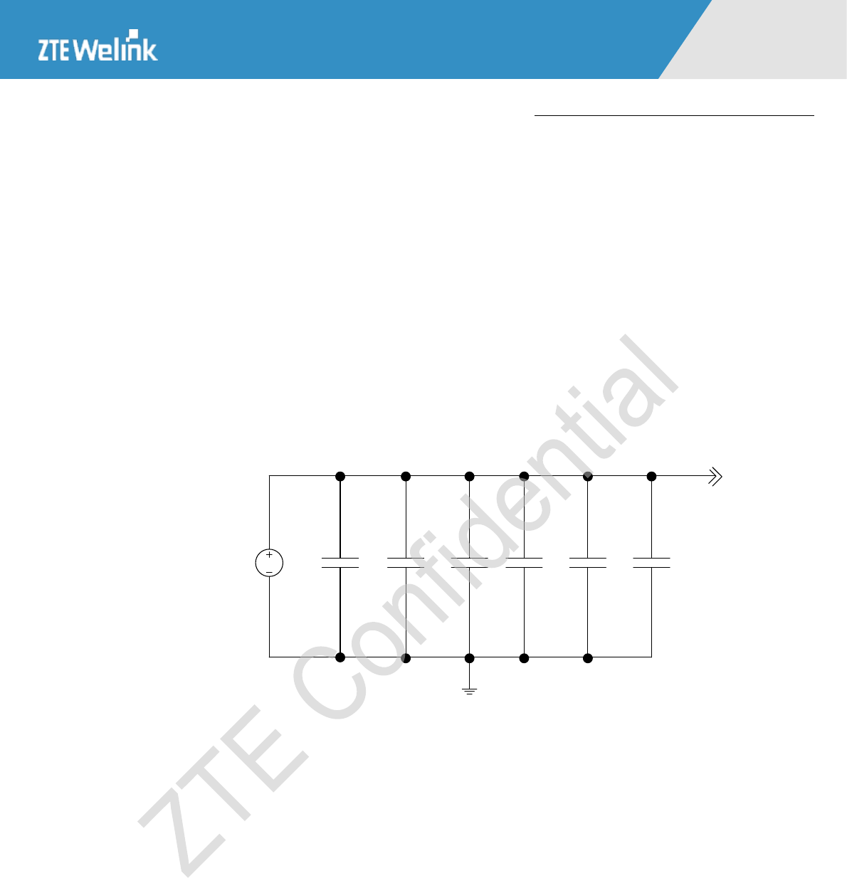
Hardware Development Guide of Module Product
All Rights reserved, No Spreading abroad without Permission of ZTEWelink 49
MF206A
The power supply capacity of system board needs to be above 2.5A to satisfy the requirement of
module peak current;
The average current on the system side needs to be above 2.0A.
When designing the PCB line, the power cable on the system board should be thick enough, and
should form a good reflux with the ground.
In the power supply circuit design, the user needs to add the large storage capacitor on the kilo level,
to guarantee the transient power supply capability, and to prevent the module from resetting and
shutting down caused by voltage fluctuation.
Figure 4–2 Add storage capacitor to Module power supply terminal
DC3.8V
VDD_3V8
0.47uF
22uF
330uF
2200uF
330uF
C1
C2
C3
C4
C5
C6
330uF
Add storage capacitor to Module power supply terminal to ensure the system instantaneous power capacity
4.4 Recommended Power Reference Circuit
Option one:
Use DC\DC switching power supply and large storage capacitor on the kilo level to ensure the normal operation
of the RF power amplifier to withstand these current peaks without big voltage drops.
Advantage:
Can provide well transient current under 2G weak signal environment to satisfy modules requirements, to
prevent device from shutdown and Ports re-enumeration as a consequence of the supply voltage drop.
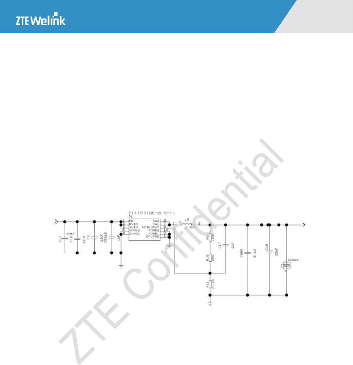
Hardware Development Guide of Module Product
All Rights reserved, No Spreading abroad without Permission of ZTEWelink 50
MF206A
The over-current capability requirement of DC/DC switching power supply need to be above 3A, for
example,ZI1153, AAT2138 and so on.
Input voltage range of ZI1153 is: 2.5~5.5V,output voltage range of ZI1153 is from 0.6V to VIN( input
voltage).
Input voltage range of AAT2138is: 2.7~5.5V,output voltage range of AAT2138 is from 3.3~5.5V.
As shown in the Figure below, use DC/DC switching power supply ZI1153 as the buck chip. Place a tantalum
capacitor of 330μF at the input of the chip. Place a 2200μF capacitor or place several 330μF tantalum
capacitors in parallel. This circuit fully meets the module power requirements. (If the user’s PCB size is limited,
the output of buck chip can place three more 330μF tantalum capacitors of which the total capacity is more than
1000μF)
Figure 4–3 DC/DC Switching Power Supply
Vin=5V Vout=3.8V
Option two:
Use LDO as the buck chip. The over-current capability of LDO is above 3A. As the poor transient response of
linear regulator, large capacitors should be placed at the input and output of LDO. The output of LDO, place a
capacitors above 2000μF. The reference power supply circuit design with LDO is as shown in Figure below.
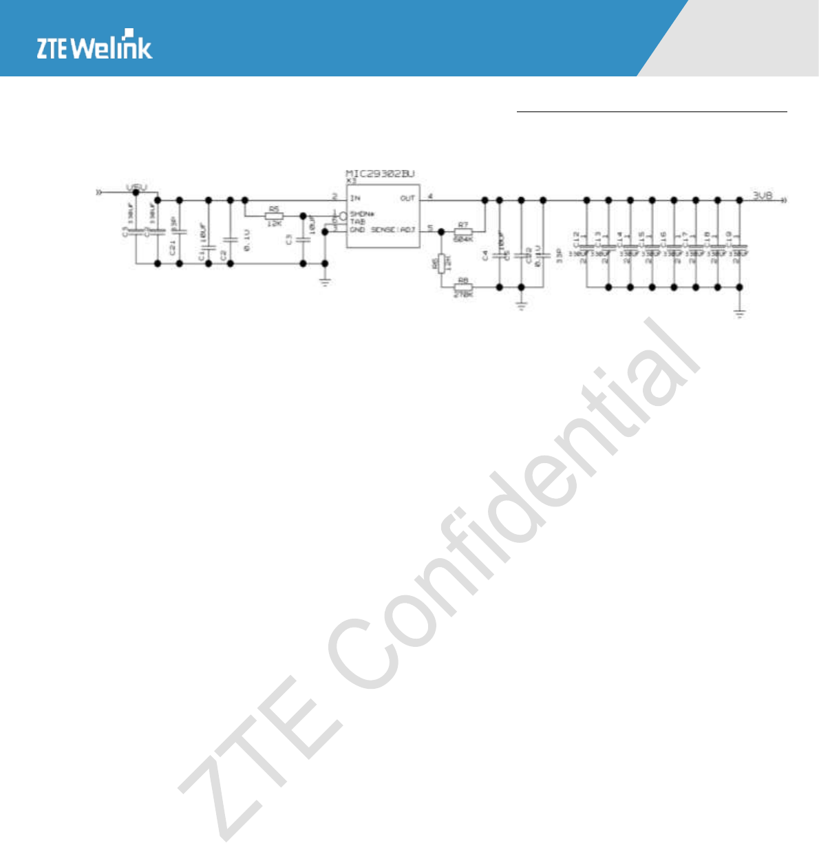
Hardware Development Guide of Module Product
All Rights reserved, No Spreading abroad without Permission of ZTEWelink 51
MF206A
Figure 4–4 LDO Power Supply
4.5 PCB Layout Guideline of Power Supply
As seen on the electrical design guidelines the power supply shall have a low ESR capacitor on the output to cut
the current peaks and a protection diode on the input to protect the supply from spikes and polarity inversion.
The placement of these components is crucial for the correct working of the circuitry. A misplaced component
can be useless or can even decrease the power supply performances. The users of ZTEWelink modules should do
as the following guidelines in the process of power supply PCB line designing:
The use of a good common ground plane is suggested.
The placement of the power supply on the board should be done in such a way to guarantee that the high current
return paths in the ground plane are not overlapped to any noise sensitive circuitry as the microphone
amplifier/buffer or earphone amplifier.
The power supply input cables should be kept separate from noise sensitive lines such as
microphone/earphone/RF cables.
The Bypass low ESR capacitor must be placed close to the ZTEWelink module power input pads, or in the case
the power supply is a switching type it can be placed close to the inductor to cut the ripple provided the PCB
trace from the capacitor to the module is wide enough to ensure a dropless connection even during the 2.5A
current peaks.
The protection diode must be placed close to the input connector where the power source is drained.
The PCB traces from the input connector to the power regulator IC must be wide enough to ensure no voltage
drops occur when the 2.5A current peaks are absorbed. Note that this is not made in order to save power loss but
especially to avoid the voltage drops on the power line at the current peaks frequency that will reflect on all the

Hardware Development Guide of Module Product
All Rights reserved, No Spreading abroad without Permission of ZTEWelink 52
MF206A
components connected to that supply, introducing the noise floor at the burst base frequency. For this reason
while a voltage drop of 300-400 mV may be acceptable from the power loss point of view, the same voltage
drop may not be acceptable from the noise point of view. If your application doesn't have audio interface but
only uses the data feature of the ZTEWelink module, then this noise is not so disturbing and power supply layout
design can be more forgiving.
The PCB traces to the ZTEWelink module and the Bypass capacitor must be wide enough to ensure no
significant voltage drops occur when the 2.5A current peaks are absorbed. This is for the same reason as
previous point. Try to keep this trace as short as possible.
The PCB traces connecting the Switching output to the inductor and the switching diode must be kept as short as
possible by placing the inductor and the diode very close to the power switching IC (only for switching power
supply). This is done in order to reduce the radiated field (noise) at the switching frequency (100-500 kHz
usually).

Hardware Development Guide of Module Product
All Rights reserved, No Spreading abroad without Permission of ZTEWelink 53
MF206A
5 RF Antenna Design Guide
The antenna connection and board layout design are the most important aspect in the full product design as they
strongly affect the product overall performances, hence read carefully and follow the requirements and the
guidelines for a proper design.
5.1 Antenna Types
Antenna types and modes are different according to the different ID designs and circuit layout designs of the
product itself. You can choose the antenna type and mode according to the estimation result by antenna
engineers.
1. For PAD products, because the product itself has low sections, usually printed antennas are used as
the antenna mode (the antenna wiring is printed on a thin PCB board), and IFA plus parasitic units or
monopole plus parasitic units are used as the antenna type.
2. For CPE products, because most products of this type have a large size, the available space for
antennas is also relative large. Thus, this type of products usually adopts the mode of PC racks plus FPC
antennas or PC racks plus bullet antennas. IFA plus parasitic units or monopole plus parasitic units are used
as the antenna type.
3. If the product supports external antenna, then switch between the external antenna and internal
antenna must be using mechanical switches instead of electronic switches.
5.2 Antenna RF Cable and RF Connector
5.2.1 RF Connector
There are two interfaces on the RF antenna of module: main antenna interface, and GPS antenna. The main
antenna supports two access modes of RF signal: by LGA wielding panel mode and by RF connector mode. The
GPS antenna only supports the access mode of LGA wielding panel. Figure 5-1 is the main antenna connector
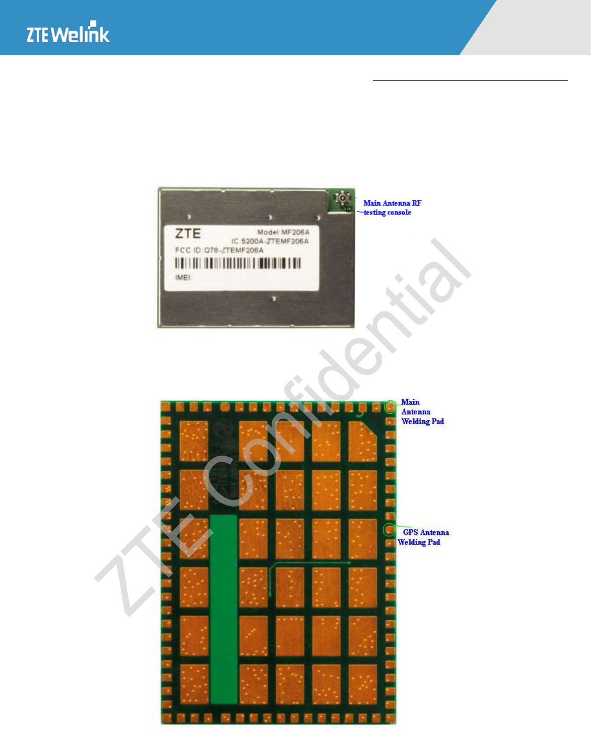
Hardware Development Guide of Module Product
All Rights reserved, No Spreading abroad without Permission of ZTEWelink 54
MF206A
interface, and Figure 5-2 is the Interface of Main Antenna and GPS Antenna Welding Pad. Figure 5-3 shows the
main antenna RF connector. Currently, ZTEWelink module adopts the ECT818000157 RF connector testing
console from ECT Company.
Figure 5–1 Main Antenna RF Connector Interface
Figure 5–2 Interface of Main Antenna and GPS Antenna Welding Pad
Hardware Development Guide of Module Product
All Rights reserved, No Spreading abroad without Permission of ZTEWelink 55
MF206A
Figure 5–3 RF Interface Testing Console
Figure 5–4 Profile Dimensions of RF antenna console
If the main antenna is access by the RF connector, the using of corresponding cables of RF interface are
recommended. When this connection mode is adopted, the RF antenna connector can be directly inserted to the
RF testing console of the module, so it saves the connection between the RF port and the antenna interface.
If the main antenna is accessed by the LGA wielding panel, the RF main antenna wield pane of the module itself
needs to be connected to the antenna interface on main board via the wield pane and micro stripline or stripline.
The micro stripline or stripline is designed according to the 50ohm impedance, and the dual-L model matching
circuit is reserved.
RF interface on ZTEWelink module is ECT818000157. Because this type of RF interfaces requires RF cables
with smaller diameters and larger consumptions, it is usually recommended not to directly connect RF
connectors of antenna RF cables with RF interfaces on the module, and it is recommended to convert them into

Hardware Development Guide of Module Product
All Rights reserved, No Spreading abroad without Permission of ZTEWelink 56
MF206A
common interfaces by conversion circuits, such as ECT818000071 of I-PEX and U.FL-R-SMT-1(80) of
HIROSE.
The design of GPS antenna is consistent with the main antenna, and its efficiency index is allowed to be 3dB
lower. The separation degree between the main antenna and the diversity antenna is required to be greater than
12dB.
5.2.2 RF Cable
If the diameter of RF cables used by the antenna is different, its consumption is also different. During the
2G/3G/LTE communication, usually RF cables with a diameter of 1.37mm or 1.13mm are adopted. It is
recommended to select the RF coaxial cable with a diameter of 1.37mm because it has less consumption. There
are many manufacturers of RF cables, such as GBE in Taiwan, Shenyu and Yuanda in China mainland,
SUMITOMO and Shin Din in Japan. All of these manufacturers provide RF cables of more than two
specifications. The following tables describe RF cables of several specifications.
The Standard Value of cable (RF137XR4 of GBE, RF-1.37 of Shenyu, 0.8DS-PBM(1.35) of SUMITOMO)
consumption is shown as Table 5-1 below (Unit: dB/m):
Table 5–1 The Cable Consumption
Frequency
RF137XR4 of GBE
RF-1.37 of Shenyu
0.8DS-PBM(1.35)
0.4GHz
1.0
--
--
0.8GHz
1.5
--
--
1.0GHz
1.6
≤1.7
≤1.5
1.5GHz
2.0
--
--
2.0GHz
2.3
≤2.5
≤2.2
2.4GHz
--
--
≤2.6
3.0GHz
2.9
≤3
≤2.8
4.0GHz
--
≤3.5
≤3.4
5.0GHz
--
≤4
≤3.8
5.2GHz
4.0
--
--
5.8GHz
4.2
--
--
6.0GHz
4.3
≤4.5
≤4.3
Hardware Development Guide of Module Product
All Rights reserved, No Spreading abroad without Permission of ZTEWelink 57
MF206A
Because RF cables used by the antenna inevitably introduce certain loss, it is necessary to consider the wiring
length of RF cables during the design of module position and antenna position. It is recommended to control the
length within the loss range of 0.5 dB (HF). During the wiring design of antenna RF cables, avoid right angle,
pressed and wearing.
The recommended receptacles Mode of ECT 818000157 is ECT 818000160 as shown below:
Figure 5–5 Recommended Receptacles Mode for module
5.3 Design of Antenna
5.3.1 Preliminary Antenna Evaluation
The antenna is a sensitive device and its performance is greatly affected by external environments. The radiation
performance of the antenna is affected by the mainboard dimensions, antenna position, occupied space size of
the antenna, and the grounding of surrounding components of the antenna. Besides, the fixed assembly of the
antenna, the wiring of RF cables on the antenna, and the fixed position of the antenna all affect the radiation
performance of the antenna too. Thus, during the preliminary design phase of an antenna, it is critical that
antenna engineers, RF engineers, baseband engineers, structure engineers, and ID engineers work together to
make an estimation for both 2D and 3D design.
The antenna interface should have an impedance of 50Ω.

Hardware Development Guide of Module Product
All Rights reserved, No Spreading abroad without Permission of ZTEWelink 58
MF206A
5.3.2 Suggested Antenna Location
During the design of the board with ZTEWelink module, the placement of components should be placed
properly, and keep the line length as short as possible, thus leading to lowest power losses possible.
Usually, the antenna position is designed according product features and antenna shall not be installed inside
metal cases. For example, for Internet laptops and PAD products, the ideal position of antennas is on the top left
corner or top right corner of the LCD, which is relatively far from the mainboard, so the electromagnetic
interference is relatively small. Besides, because it is far from human bodies, it is easy to satisfy SAR indexes.
For PAD products or Internet laptops, the ideal position is where hands rarely touch, so the impact from hand
holding is the minimum.
The above example only considers the antenna position area in a specific scenario. For the specific position, it is
critical to determine with antenna engineers, RF engineers, baseband engineers, structure engineers, and ID
engineers during the 2D/3D estimation phase according to the specific product. Antenna shall be installed also
according to antenna manufacturer instructions.
5.3.3 Suggested Antenna Occupancy Space
For different product types, because their frequency bands are different, required occupation space of the
antenna is also different. For the specific antenna space, it is critical to estimate it with antenna engineers, RF
engineers, baseband engineers, structure engineers, and ID engineers during the 2D/3D estimation phase. Taking
the PAD product with a dimension of 95 mm * 125 mm (length * width) as an example, if the antenna should
cover 824-960 MHz and 1710-2170 MHz, it is recommended to reserve the following antenna space: if the
printed antenna mode is adopted, the reserved space should be above 75mm*10mm (length*width); if the
antenna mode of PC rack plus FPC or PC rack plus spring is adopted, the reserved space should be above
70mm*10mm*3mm (length*width*height).
5.3.4 Matching Circuit of Antenna
For all products with ZTEWelink module, the antenna is basically connected to the module through RF cables
and RF connectors. This section describes two situations.
1. If the RF terminal connector of the module does not match the RF cables used by the antenna, or the
direct connection between the RF antenna mated connector of RF cables and the RF port of the module is
Hardware Development Guide of Module Product
All Rights reserved, No Spreading abroad without Permission of ZTEWelink 59
MF206A
restricted by the height, a circuit is required between them for transition. During the design of transit
circuits on the mainboard, the natural impedance of the microstrip line or stripline between the RF port of
the module and the RF port on the mainboard connected to the antenna is designed to be 50 ohm, and a
dual-L matching circuit is reserved, as shown in Figure 5-6. Use a zero-ohm resistor on the cascading
position between them.
2. If the RF connector used by the RF cable can be directly connected to the RF terminal on the module,
and the height falls within the limited range, the circuit transition between the RF port on the module and
the antenna interface can be saved, and the RF connected used by the RF cable of the antenna can be
directly connected to the RF terminal of the module.
Figure 5–6 Transition Circuit
Microstrip line or
stripline with a
natural impedance of
50 ohm
Microstrip line or
stripline with a
natural impedance of
50 ohm
Dual-L matching
network
RF coaxial cable of
the antenna
RF interface on the
antenna RF cable
and RF interface on
the mainboard
RF interface on
the module
Antenna
5.3.5 Type of Antenna RF Cable & RF Connector
The antenna RF connection cable usually adopts GBE(TW) and Shenyu (Mainland), or Japanese Somitomo and
Shin Din. The antenna RF cable usually adopts a line width of 1.37mm. The antenna RF connector usually
adopts Japanese IPX, or HRS, while the price of the latter is higher.

Hardware Development Guide of Module Product
All Rights reserved, No Spreading abroad without Permission of ZTEWelink 60
MF206A
5.4 Recommended Antenna Manufacturers
Many domestic antenna manufacturers in China can design proper matched antennas according to specific
products. This section recommends several antenna manufacturers with strong integrative strength in the mobile
terminal industry, which have powerful hardware resources and software resources, experienced antenna design
engineers, and advanced antenna test systems (including antenna Passive test, Passive OTA test, and SAR test)
to satisfy various customer requirements.
1. Ethertronics at Shanghai
2. Skycross at Shanghai
3. Laird at Beijing
4. Sherbed at Suzhou
5. Yaodeng Electronic Communication Technology (kunshan) Co., Ltd.
5.5 PCB line guidelines
The users of ZTEWelink modules should do as the following guidelines in the process of RF PCB line design:
1. Make sure that the transmission line’s characteristic impedance is 50ohm ;
2. Keep line on the PCB as short as possible, since the antenna line loss shall be less than around 0,3 dB;
3. Line geometry should have uniform characteristics, constant cross section, avoid meanders and abrupt
curves;
4. If a Ground plane is required in line geometry, that plane has to be continuous and sufficiently extended,
so the geometry can be as similar as possible to the related canonical model;
5. It is wise to surround (on both sides) the PCB transmission line with Ground, avoid having other signal
tracks facing directly the antenna line track.
6. Keep, if possible, at least one layer of the PCB used only for the Ground plane; If possible, use this
layer as reference Ground plane for the transmission line;
7. Avoid crossing any un-shielded transmission line footprint with other signal tracks on different layers;

Hardware Development Guide of Module Product
All Rights reserved, No Spreading abroad without Permission of ZTEWelink 61
MF206A
8. The ground surrounding the antenna line on PCB has to be strictly connected to the main Ground Plane
by means of via holes (once per 2mm at least), placed close to the ground edges facing line track;
9. Place EM noisy devices as far as possible from modules antenna line;
10. Keep the antenna line far away from the module power supply lines;
11. If EM noisy devices are present on the PCB hosting the ZTEWelink module, such as fast switching ICs,
take care of the shielding of the antenna line by burying it inside the layers of PCB and surround it with
Ground planes, or shield it with a metal frame cover.
5.6 Suggestions for EMC & ESD Design
5.6.1 EMC Design Requirements
During the design of the whole device, the user needs to fully consider the EMC problem caused by the signal
integrity and power integrity.
1. During the product design, it is better to separate the module from the mainboard PCB, instead of
installing the module on the ground of the mainboard. If they cannot be separated, the module should be far
from modules and components that might generate EMI, such as chip and memory, power interface, and
data cable interface.
2. Because the mainboard of PAD, CPE, and Internet laptops does not have a shielding cover, as that of
mobile terminals, to shield most circuits to avoid overflow of electromagnetic interference, you can spray
conductive paint on the surface on non-antenna areas within the structural components above and below the
mainboard, and the conductive paint should be connected to the ground on the mainboard by several points
to shield electromagnetic interference.
3. Besides, data cables of the LCD and the camera might introduce interference signals, which affect the
receiving performance of the antenna. Thus, it is necessary to wrap conductive cloth around the two data
cables and connected them to the ground.
4. RF cables of the antenna should be far from modules and components that might generate EMI, such
as chip and memory, power interface, and data cable interface. The wiring of RF cables should be close to
the ground of the mainboard.

Hardware Development Guide of Module Product
All Rights reserved, No Spreading abroad without Permission of ZTEWelink 62
MF206A
5. During the layout and wiring of peripheral circuits, for the wiring of power and signal cables, keep a
distance of 2 times of the line width, so as to effectively reduce the coupling between signals and keep a
clean reflux path for the signal.
6. During the design of peripheral power circuits, the de-coupled capacitor should be placed closed to the
module power PIN, the high-frequency high-speed circuit and the sensitive circuit should be placed far
away from the border of PCB. They should better be separated during layout, so as to reduce the
interference between them and protect the sensitive signal.
7. For the circuit or device on the side of system board that might interfere with the module, it should be
shielded during design.
5.6.2 ESD Design Requirements
MF206A is embedded on the side of system board, so the user needs to make the ESD protection during design.
For the key input/output signal interface, such as the (U)SIM card signal interface, the ESD device should be
placed closely for protection. Besides, on the side of main board, the user should reasonably design the structure
and PCB layout, guarantee that the metallic shielding shell is fully grounded, so as to leave a smooth discharge
channel for ESD.
5.7 Antenna Indexes
The module supports the AGPS/GPS function, so the system equipment needs to add the GPS antenna. The
design of GPS antenna is consistent with that of the main antenna, and its efficiency index can be 3dB lower.
The separation degree between the main antenna and the diversity antenna is required to be greater than 12dB.
The antenna index is divided into the Inactive index and Active index. The Inactive index includes S11,
efficiency, gains, orientation diagram and polarity, which can be used as the parameter measuring the
performance of the antenna itself. The Active index is also called the OTA index, including TRP (all-round
radiation power), TIS (all-round receiving sensitivity), radiation orientation diagram, which is an important
index measuring the radiation performance of the whole set (including the antenna, module, main board).

Hardware Development Guide of Module Product
All Rights reserved, No Spreading abroad without Permission of ZTEWelink 63
MF206A
5.7.1 Passive Indexes
Different products have different requirements for antenna performance. The following table describes wireless
indexes for PAD products as a reference to users, but the radiation performance of the antenna is finally
determined by Active indexes.
Table 5–2 Passive Indexes of Main Antennas on PAD Products
Frequency
824-960MHz
1710-2170MHz
VSWR
<3.5:1
<3.5:1
Maximum gains
>0dBi
>0dBi
Average gains
>-3.5dBi
>-3.5dBi
Efficiency
>40%
>40%
5.7.2 Active Indexes
Active indexes are important indexes measuring the radiation performance of the whole mobile phone (including
the antenna, module, and mainboard), thus they determine the final radiation performance of the terminal
product. However, different products have different Active indexes, and different carries have different
requirements for Active indexes as well. Thus, antenna engineers, RF engineers, baseband engineers, structure
engineers, and ID engineers should work together to estimate the performance of the board during the project
preliminary phase according to the Active indexes. There is no universal international standard for mobile
terminal products, so mobile terminals are all designed according to the carrier requirements. Table 5-3 describes
the requirement of Active indexes by ZTEWelink for Mobile Terminal Devices as a reference to users.
Table 5–3 ZTEWelink Indexes for Mobile Terminal Devices
Mode
Band
TRP(dBm)
TIS(dBm)
Free space
Free space
GSM
GSM850MHz
28
-104
GSM900MHz
28
-104
GSM1800MHz
26
-102
GSM1900MHz
26
-102
WCDMA
Band I
19
-106
Band II
19
-104.5
Band V
19
-104.5
Band VIII
19
-104.5
The Active indexes of diversity antennas are determined by the performance of diversity antennas.
Hardware Development Guide of Module Product
All Rights reserved, No Spreading abroad without Permission of ZTEWelink 64
MF206A
5.7.3 Test Methods for Whole-Set Antenna OTA
Figure 5-7 is the diagram of OTA test system of CTIA. The system is mainly composed of test chamber,
high-precision positioning system and its controller, Windows based PC running test software and RF test
instruments with automatic test program. The main RF instruments are integrated RF test equipment, Spectrum
Analyzer, Network Analyzer.
The radio equipments, Relay Switch Unit and PC with automatic test software are communicated via GPIB
interface.
Figure 5–7 The OTA test system of CTIA

Hardware Development Guide of Module Product
All Rights reserved, No Spreading abroad without Permission of ZTEWelink 65
MF206A
6 Electric Feature
6.1 Power Supply
The external power supply must be connected to VPH_PWR signals and must fulfill the following requirements:
The input voltage range of module is DC 3.4V~4.2V, and the typical value is 3.8V as shown in Table6-1.
Table 6–1 Input Voltage
Parameter
Min
Typical
Max
Input voltage
3.4V
3.8V
4.2V
6.2 Working Current
The working current range of module is as shown in Table 6-2 to Table 6-4. The IDLE mode indicates the power
consumption of the module when there is no service but the module is interactive with network. The table also
provides the working current range under GSM and WCMA mode when there is data service.
Table 6–2 Averaged standby DC power consumption
Mode
Bands
Test value (mA)
Remark
/WCDMA
Band I (IMT2100)
2.3
Standby mode
Band II (PCS1900)
2.3
Band V (850M)
2.4
GSM/GPRS/EDGE
GPRS 1900
5.4
Standby mode
GPRS 1800
5.4
GPRS 900
5.6
GPRS 850
5.9
Note: assumes USB bus is fully suspended during measurements. Under different
environments, the testing results might be slightly different. Take the actual situation as the
reference.
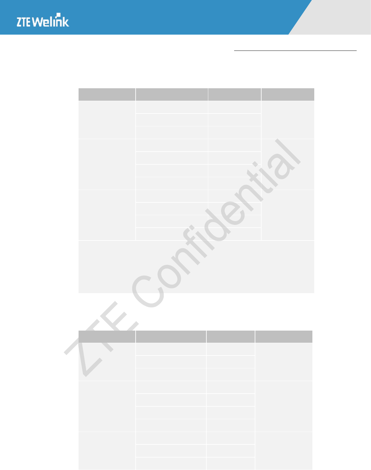
Hardware Development Guide of Module Product
All Rights reserved, No Spreading abroad without Permission of ZTEWelink 66
MF206A
Table 6–3 Averaged idle mode DC power consumption
Mode
Bands
Test value (mA)
Remark
UMTS
Band I (IMT2100)
68
Idle mode
Band II (PCS1900)
60
Band V (850M)
59
GPRS
GPRS1900
51
Idle mode
GPRS1800
46
GPRS900
24
GPRS850
21
EDGE
EDGE1900
39
Idle mode
EDGE1800
23
EDGE900
47
EDGE850
41
Note: The IDLE mode indicates the power consumption of the module when there is no
service. But the module is interactiving with the network such as network registration, and
USB is active.
The above values are the average of some test samples. Under different environments, the
testing results might be slightly different. Take the actual situation as the reference.
Table 6–4 Averaged DC power consumption in working state
Mode
Bands
Test value (mA)
Remark
UMTS
Band I (IMT2100)
468
Acquired under the
maximum
transmission power
Band II (PCS1900)
475
Band V (850M)
376
GPRS
GPRS1900
287
Acquired under the
maximum
transmission power
GPRS1800
275
GPRS900
352
GPRS850
363
EDGE
EDGE1900
208
Acquired under the
maximum
transmission power
EDGE1800
202
EDGE900
210

Hardware Development Guide of Module Product
All Rights reserved, No Spreading abroad without Permission of ZTEWelink 67
MF206A
EDGE850
215
Note: The above average current is acquired under the maximum transmission power.
Under different environments, the testing results might be slightly different. Take the
actual situation as the reference.
NOTE:
The above average current is acquired under the maximum transmission power. Under different
environments, the testing results might be slightly different. Take the actual situation as the reference.

Hardware Development Guide of Module Product
All Rights reserved, No Spreading abroad without Permission of ZTEWelink 68
MF206A
7 Technical Index of Radio Frequency
Test Environment:
Test instrument: Agilent 8960
Power supply: Agilent 66319D
RF cable for testing
Cable length: About 15 cm
Compensation for WCDMA 850 MHz or WCDMA 900 MHz: 0.6 dB
Compensation for WCDMA 2100 MHz or WCDMA 1900 MHz: 0.8 dB
NOTE:
The compensation for different frequency bands relates to the cable and the test environment.
The instrument compensation needs to be set according to the actual cable conditions.
7.1 Index of RF under UMTS Mode
7.1.1 UMTS (WCDMA)
The RF index should be tested strictly in accordance with the related testing specifications of 3GPP. The RF
indexes of UMTS2100/1900/850 should satisfy the requirements of 3GPP TS 34.121 protocol.
Hardware Development Guide of Module Product
All Rights reserved, No Spreading abroad without Permission of ZTEWelink 69
MF206A
7.1.2 Acquiring Radio Frequency Index
The testing of radio frequency index should strictly follow the specified testing specifications of 3GPP. In
particular, when carrying out the acceptance test of related indexes, make sure to perform the test in a
well-shielded environment.
7.1.3 Maximum Transmission Power
Under the normal testing environment, the maximum transmission power of UMTS2100/1900/850(900) should
satisfy the requirements in Table 7-1.
Table 7–1 Maximum Transmission Power
Operating Band
level
3GPP Protocol Claim (dBm)
Test value
UMTS850
Class 3
+24dBm +1/-3dBm
22.4dBm
UMTS1900
Class 3
+24dBm +1/-3dBm
22.3dBm
UMTS2100
Class 3
+24dBm +1/-3dBm
22.3dBm
7.1.4 Receiving Sensibility
The receiving sensitivity is a key parameter that indicates the receiver performance of module. The receiving
sensitivity is the weakest signal that the module at the antenna port can receive. At the same time the BER (Bit
Error Rate) must meet the 3GPP TS 34.121protocol requirements in case of the minimum signal. The test value
of UMTS2100/1900/850(900) receiving sensibility is shown in the Table 7-2.
Table 7–2 Reference Table of Receiving Sensitivity
Operating Band
Unit
3GPP Protocol Claim
Test value
UMTS850
dBm/3.84 MHz
≤-104.7dBm
-109dBm
UMTS1900
dBm/3.84 MHz
≤-104.7dBm
-109dBm
UMTS2100
dBm/3.84 MHz
≤-106.7dBm
-110dBm

Hardware Development Guide of Module Product
All Rights reserved, No Spreading abroad without Permission of ZTEWelink 70
MF206A
7.1.5 Spurious Emission Index
The spurious emission index of UMTS2100/1900/850(900) should comply with the requirements in 3GPP TS
34.121 protocol, as illustrated below. And the test result of module in UMTS mode meets the requirement in
Table 7-3.
Table 7–3 Spurious Emission Index
Frequency Band
Resolution Bandwidth
Minimum Requirement
9 kHz f < 150 kHz
1 kHz
-36 dBm
150 kHz f < 30 MHz
10 kHz
-36 dBm
30 MHz f < 1000 MHz
100 kHz
-36 dBm
1 GHz f < 12.75 GHz
1 MHz
-30 dBm
7.2 Index of RF under GPRS/GSM/EDGE Mode
The RF indexes of GSM/GPRS/EDGE850/900/1800/1900 should satisfy the requirements of 3GPP TS 05.05
protocol.
7.2.1 Output Transmission Power
The maximum output transmission power of GSM850/900/1800/1900 (GMSK/8PSK) should comply with the
requirements of 3GPP TS 05.05 4.1 protocol, as shown in Table 7-4 indicates the power level of each frequency
band.
Table 7–4 Output Transmission Power of GSM850/900/1800/1900 (GMSK)
Operating Band
Power level
3GPP Protocol Claim (dBm)
Test value
GSM850
Class 4
+33dBm±2dBm
32.0dBm
GSM900
Class 4
+33dBm±2dBm
32.0dBm
GSM1800
Class 1
+30dBm ±2dBm
29.0dBm
GSM1900
Class 1
+30dBm ±2dBm
29.0dBm
Hardware Development Guide of Module Product
All Rights reserved, No Spreading abroad without Permission of ZTEWelink 71
MF206A
7.2.2 Receiving Sensibility
The receiving sensitivity is a key parameter that indicates the receiver performance of module. The receiving
sensitivity is the weakest signal that the module at the antenna port can receive. At the same time the BER (Bit
Error Rate) must meet the 3GPP TS 05.05 6.2 protocol requirements in case of the minimum signal. The test
value of GSM850/900/1800/1900 receiving sensibility is shown in the Table 7-5.
Table 7–5 Reference Table of Receiving Sensitivity
Operating Band
Unit
3GPP Protocol Claim
Test value
GSM850
dBm/3.84 MHz
≤-102dBm
-108dBm
GSM900
dBm/3.84 MHz
≤-102dBm
-108dBm
GSM1800
dBm/3.84 MHz
≤-102dBm
-107dBm
GSM1900
dBm/3.84 MHz
≤-102dBm
-107dBm
7.2.3 Spurious Emission Index
The spurious emission index of GSM850/900/1800/1900 (GMSK) should comply with the requirements of
3GPP TS 4.3.2.1 protocol, as shown in the table below.
The power measured in bandwidth of 9kHz to 1GHz shall be no more than -36 dBm.
The power measured in bandwidth of 1GHz to 12.75GHz shall be no more than -30dBm.
And the test result of module in GPRS/GSM/EDGE mode meets the requirement above.

Hardware Development Guide of Module Product
All Rights reserved, No Spreading abroad without Permission of ZTEWelink 72
MF206A
8 Related Test & Test Standard
8.1 Testing Reference
The related tests of module comply with the IEC standard, including the equipment running under high/low
temperature, storage under high/low temperature, temperature shock and EMC. Table 8-1 is the list of testing
standard, which includes the related testing standards.
Table 8–1 Testing Standard
Test Standard
Document Reference
IEC6006826
Environmental testing-Part2.6:Test FC: Sinusoidal Vibration
IEC60068234
Basic environment testing procedures part2.
IEC60068264
Environmental testing-part2-64: Test FH: vibration, broadband random and
guidance.
IEC60068214
Environmental testing-part 2-14: Test N:change of temperature.
IEC60068229
Basic environmental testing procedures-part2: Test EB and guidance.
IEC6006822
Environmental testing-part2-2:Test B:dry heat
IEC6006821
Environment testing-part2-1: Test A: cold.
GB/T 15844.2
MS telecommunication RF wireless phone-set environment requirement &
experimental method – part 4: Strict level of experimental condition
GB/T 2423.17
Basic environment experiment of electronic products-Experiment Ka: Salt
mist experiment method
GB/T 2423.5
Basic environment experiment of electronic products-Part2:Experiment
method Try Ea & Introduction: Shock
GB/T 2423.11
Basic environment experiment of electronic products-Part2:Experiment
method Try Fd: Broad frequency band random vibration (General
requirement)
TIA/EIA 603 3.3.5
TIA Standard-part3-5:Shock Stability

Hardware Development Guide of Module Product
All Rights reserved, No Spreading abroad without Permission of ZTEWelink 73
MF206A
NOTE:
1. IECL International Electro technical Commission;
2. GB/T: Recommended national standard
8.2 Description of Testing Environment
The working temperature range of module is divided into the normal working temperature range and the extreme
working temperature range. Under the normal working temperature range, the testing result of RF complies with
the requirements of 3GPP specifications, and its function is normal. Under the extreme temperature range, the
RF index basically complies with the 3GPP specifications, and the quality of data communication is affected to a
certain extent, but its normal function is not affected. The module has passed the EMC test. Table 8-2 is the
requirement for the testing environment, and Table 8-3 lists out the instruments and devices that might be used
during the test.
WARNING:
Table 6-2 lists the extreme working conditions for the module. Using the module beyond these conditions
may result in permanent damage to the module.
Table 8–2 Testing Environment
Working
Condition
Min
Temperature
Max
Temperature
Remark
Normal
working
condition
-30°C
75°C
All the indexes are good.
Extreme
working
condition
-40°C
85°C
Some indexes become
poorer.
Storage
-45°C
90°C
Storage environment of
module

Hardware Development Guide of Module Product
All Rights reserved, No Spreading abroad without Permission of ZTEWelink 74
MF206A
Table 8–3 Testing Instrument & Device
Testing Item
Instrument & Device
RF test
Comprehensive testing device
RF cable
Tower antenna
Microwave darkroom
High/Low-temperature
running & storage test
High/Low-temperature
experimental box
Temperature shock test
Temperature shock
experimental box
Vibration test
Vibration console
8.3 Reliability Testing Environment
The reliability test includes the vibration test, high/low-temperature running, high/low-temperature storage and
temperature shock experiment test. Refer to Table 8-4 for the specific parameters.
Table 8–4 Reliability Features
Test Item
Test Condition
Test Standard
Random vibration
Frequency range: 5-20Hz, PSD:1.0m2/s3
Frequency range: 20-200Hz, -3dB/oct
3 axis, 1 hour for each axis
IEC 68-2-6
Temperature shock
Low temperature: -40°C ±2°C
High temperature: +80°C ±2°C
Temperature changing period: less than
30seconds
Test duration: 2 hours
Cycle: 10
IEC 68-2-14 Na
High-temperature
running
Normal high temperature: 75 °C
Extreme high temperature: 85°C
Duration: 24 hours
ZTE standard
Low-temperature
running
Normal low temperature: -30°C
Extreme low temperature: -40°C
Duration: 24 hours
ZTE standard
Hardware Development Guide of Module Product
All Rights reserved, No Spreading abroad without Permission of ZTEWelink 75
MF206A
High temperature &
high humidity
Temperature: +60°C
Humidity: 95%
Duration: 48 hours
ZTE standard
High temperature
storage:
Temperature: 90°C
Duration: 24 hours
IEC 68-2-1 Ab
Low temperature
storage:
Temperature: -45°C
Duration: 24 hours
IEC 68-2-2 Bb
NOTE:
When the module works at the normal temperature, all its RF indexes comply with the 3GPP specifications.
When the module works at extreme temperature, certain RF indexes do not comply with the 3GPP
specifications.
8.4 Reliability Testing Result
Table 8–5 Temperature Testing Result Under Windless Environment
Mode
Temperature
Voltage
Transmission
Power
Duration
Testing
Result
GPRS Class 10
+25℃
(3.8±10%)V
Max
≥1hour
Pass
EDGE Class 12
+25℃
(3.8±10%)V
Max
≥1 hour
Pass
WCDMA
+25℃
(3.8±10%)V
Max
≥1 hour
Pass
Table 8–6 High/Low-temperature Running & Storage Testing Result
Test Item
Test Condition &
Standard
Test Content
Test
Result
Random vibration
Refer to Table 8-4
RF test & function test
Pass
Temperature shock
Refer to Table 8-4
RF test & function test
Pass
Low-temperature
working
Refer to Table 8-4
RF test & function test
Pass
High-temperature
working
Refer to Table 8-4
RF test & function test
Pass
Extreme low-
temperature working
Refer to Table 8-4
RF test & function test
Pass

Hardware Development Guide of Module Product
All Rights reserved, No Spreading abroad without Permission of ZTEWelink 76
MF206A
Extreme
high-temperature
working
Refer to Table 8-4
RF test & function test
Pass
Low-temperature
storage
Refer to Table 8-4
RF test & function test
Pass
High-temperature
storage
Refer to Table 8-4
RF test & function test
Pass

Hardware Development Guide of Module Product
All Rights reserved, No Spreading abroad without Permission of ZTEWelink 77
MF206A
9 Design Guide
This chapter provides the general design guide for module, used as a reference for the user during the design
process, so that the product can reach better performance.
9.1 General Design Rule & Requirement
When the user is designing the peripheral circuits of module, he needs to first guarantee that the external circuit
has the sufficient power supply capability, and the USB of high-speed signal cable is required to have 90ohm
differential resistance. For the common signal interface, it is required to design according to ZTEWelink
requirements, which needs to comply with the power level of interface signal, so as to prevent the impedance
from damaging the module. The RF index of this product itself is good, and the user needs to design the antenna
circuit of the main board and make the corresponding impedance control. Otherwise, the RF index of the whole
set will be affected.
9.2 Suggestions for PCB Wielding Panel Design
When the user is designing the encapsulation wielding panel on main board, the 30 heat wielding panels in the
center are recommended to be designed according to the dimensions as described in Figure 9-1. The surrounding
78 wielding panels should be extended by more than 0.3mm, and the other three sides of the wielding panel are
extended by 0.05mm. For the right angles of wielding panels for the main antenna PIN1 and GPS antenna PIN70,
they are recommended to be rounded into a round angel with a radius of 0.3mm. In this way, it is convenient for
the import of interference and the radiation of RF signal. The Recommended PCB Wielding Panel Design is
shown in Figure 9-1 (Unit:mm).
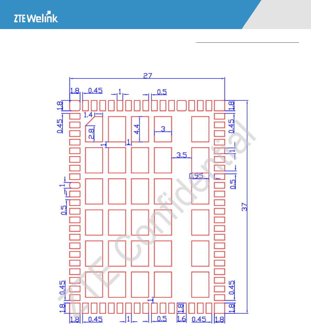
Hardware Development Guide of Module Product
All Rights reserved, No Spreading abroad without Permission of ZTEWelink 78
MF206A
Figure 9–1 Recommended PCB Wielding Panel Design
9.3 Suggestions for Heat-dissipation Design
The module will dissipate heat during the working process, and might also be affected by other high-temperature
devices. The heat dissipation is taken into full consideration during the product design, as 30 heat wielding

Hardware Development Guide of Module Product
All Rights reserved, No Spreading abroad without Permission of ZTEWelink 79
MF206A
panels are reserved in the center of the module. During the connection with the system board, make sure that
these wielding panes are grounded well, which is greatly helpful to heat conductivity and heat balance, and is
greatly beneficial to the electric performance of the whole set as well.
NOTE:
1. Keep this product away from heat-dissipation devices with high power, to prevent the temperature of the
module from being too high.
2. Do not put the module close to the large heat-dissipation devices, such as CPU or bridge. The high
temperature will affect the RF performance.
9.4 Recommended Product Upgrading Plan
It’s recommended to use the one-click software upgrade tool to upgrade through the USB port provided by
ZTEWelink in the Windows system. If the customer wants to upgrade the module in other operation systems,
ZTEWelink provides the corresponding reliable tools as well.
.
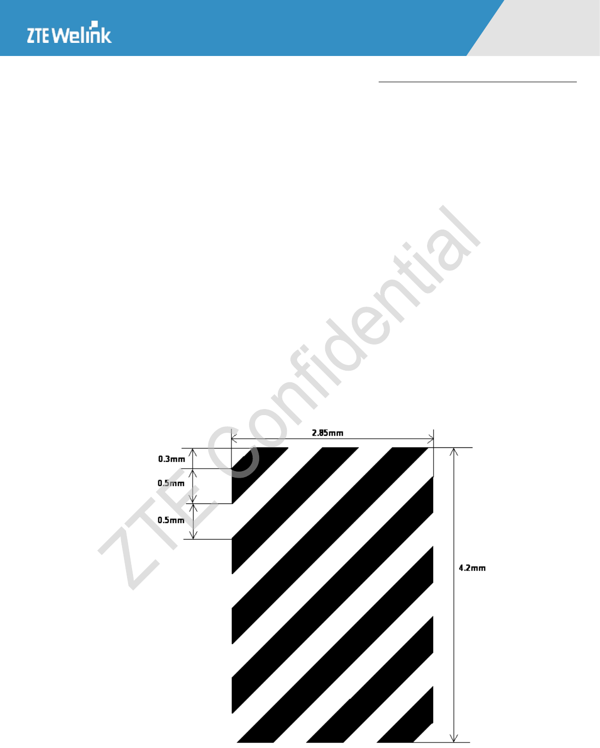
Hardware Development Guide of Module Product
All Rights reserved, No Spreading abroad without Permission of ZTEWelink 80
MF206A
10 Manufacturing Guide
10.1 Design of Steel Mesh
During the design of steel mesh, note:
1. When manufacturing the steel mesh of thermal pad on the bottom of the module, narrow the mouth of
the steel mesh of the original size, so as to reduce the risk of shortcut between the module thermal and
the peripheral PINs. This method is effective.
2. It is recommended to design to the mouth of steel mesh on the thermal pad wielding panel to the lattice
form. Figure 10-1 shows the recommended pattern for the steel mesh.
Figure 10–1 Recommended Pattern of Steel Mesh on Wielding panel
.
Hardware Development Guide of Module Product
All Rights reserved, No Spreading abroad without Permission of ZTEWelink 81
MF206A
10.2 Furnace Temperature Curve
The furnace temperature curve greatly affects the wielding quality and the material status, so it needs to be paid
great attention to. The temperature increasing speed cannot be too fast, with the increase speed from the room
temperature to 150℃ less than 3℃/second. At the same time, if the temperature is above 217℃, the duration
should be kept within 70 seconds, while the interim value 55 seconds is ideal. Otherwise, the great temperature
shock will make certain devices ineffective, causing the quality to decrease and the maintenance difficulty to
increase. At the same, keep the precise maximum temperature to be below 245℃, as certain materials (such as
the crystal) might crack under the high temperature and won’t vibrate any more, so the product function is
affected. Refer to Table 10-1 for the detailed requirements setting of furnace temperature curve, refer to Figure
10-2 for the furnace temperature curve and the testing result.
Table 10–1 Curve Temperature Curve Parameter Setting
Lead-free Curve Temperature Curve
Phase
Temperature
Duration
Pre-heat
Temperature is
increased from room
temperature to 150℃
Temperature
increasing ratio
<3℃/second
Temperature keeping
150℃~200℃
40~110 seconds
Wielding
Greater than 217℃
40~70 seconds
Above 230℃
15~45 seconds
Peak temperature
MAX: 245℃
MIN: 230℃
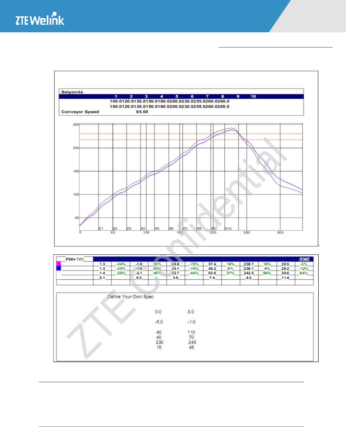
Hardware Development Guide of Module Product
All Rights reserved, No Spreading abroad without Permission of ZTEWelink 82
MF206A
Figure 10–2 Furnace Temperature Curve Reference Diagram
Company: ZTE
Furnace:
Place: SMTMobile phone R&D line 1
Process limit:
(Degree centigrade)
Temperature range
Upper temperature range
Lower temperature range
(cm per minute)
Degree centigrade
Seconds
Module edge point
Module bottom
Chip
Temperature difference
Process limit
Butter of antimony:
Statistic name Lower limit Upper limit
Maximum temperature ascending slope (target: 2.0)
(Time distance = 20 seconds)
Maximum temperature descending slope
(Time distance = 20 seconds)
Preheat time 150200C
Time of the reflow temperature or above271C
Maximum temperature
Time of the temperature above 230C
Degree per second
Degree per second
Degree centigrade
Seconds
Seconds
Seconds
Unit
Upper limit
Preheat time 150200C Time of the reflow
temperature or above271C
Maximum temperature
ascending slope Maximum temperature
descending slope Total time
NOTE:
More Guide Information about SMT & Baking about the Manufacturing process, please refer to the
document named SMT & Baking User Guide of ZTEWelink LGA Module Products.pdf
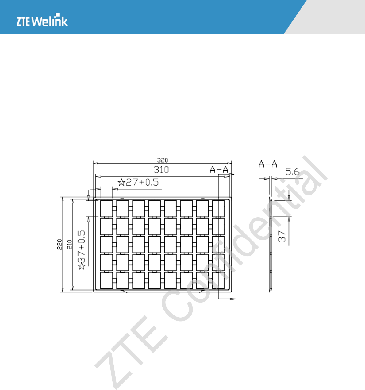
Hardware Development Guide of Module Product
All Rights reserved, No Spreading abroad without Permission of ZTEWelink 83
MF206A
10.3 Package System
The modules are packaged on trays of 40 pieces each. These trays can be used in SMT processes for pick &
place handling.
The dimensions tolerance of tray is between 1mm except the dimensions with ☆ in the Figure below (and the
unit of dimensions is mm):
Figure 10–3 The dimensions of Package tray
The package process of modules is shown as the Figure below:
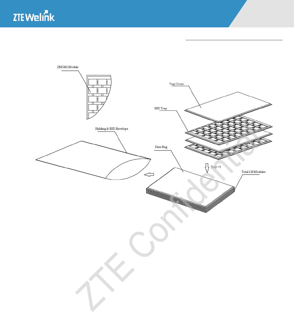

Hardware Development Guide of Module Product
All Rights reserved, No Spreading abroad without Permission of ZTEWelink 85
MF206A
11 Safety Information
The following safety precautions must be observed during all phases of the operation, such as usage, service or
repair of any cellular terminal incorporating module. Manufacturers of the cellular terminal should send the
following safety information to users, operating personnel and to incorporate these guidelines into all manuals
supplied with the product.
The use of this product may be dangerous and has to be avoided in the following areas:
Where it can interfere with other electronic devices in environments such as hospitals, aircrafts, airports, etc,
switch off before boarding an aircraft. Make sure the cellular terminal is switched off in these areas. The
operation of wireless appliances in the hospitals, aircrafts and airports are forbidden to prevent interference
with communication systems.
Areas with potentially explosive atmospheres including fuelling areas, below decks on boats, fuel or
chemical transfer or storage facilities, areas where the air contains chemicals or particles such as gasoline
stations, oil refineries, etc make sure that wireless devices are turned off.
It’s the responsibility of users to enforce other country regulations and the specific environment regulations. And
ZTEWelink does not take on any liability for customer failure to comply with these precautions.
Federal Communication Commission Interference Statement
This device complies with Part 15 of the FCC Rules. Operation is subject to the following two conditions:
(1) This device may not cause harmful interference, and (2) this device must accept any interference
received, including interference that may cause undesired operation.
This equipment has been tested and found to comply with the limits for a Class B digital device,
pursuant to Part 15 of the FCC Rules. These limits are designed to provide reasonable protection
against harmful interference in a residential installation. This equipment generates, uses and can
radiate radio frequency energy and, if not installed and used in accordance with the instructions, may
cause harmful interference to radio communications. However, there is no guarantee that interference
will not occur in a particular installation. If this equipment does cause harmful interference to radio or

Hardware Development Guide of Module Product
All Rights reserved, No Spreading abroad without Permission of ZTEWelink 86
MF206A
television reception, which can be determined by turning the equipment off and on, the user is
encouraged to try to correct the interference by one of the following measures:
● Reorient or relocate the receiving antenna.
● Increase the separation between the equipment and receiver.
● Connect the equipment into an outlet on a circuit different from that to which the receiver is
connected.
● Consult the dealer or an experienced radio/TV technician for help.
FCC Caution:
Any changes or modifications not expressly approved by the party responsible for compliance could
void the user's authority to operate this equipment.
This transmitter must not be co-located or operating in conjunction with any other antenna or
transmitter.
Radiation Exposure Statement:
This equipment complies with FCC radiation exposure limits set forth for an uncontrolled environment.
This equipment should be installed and operated with minimum distance 20cm between the radiator &
your body.
This device is intended only for OEM integrators under the following conditions:
1) The antenna must be installed such that 20 cm is maintained between the antenna and
users, and the maximum antenna gain allowed for use with this device is 5 dBi.
2) The transmitter module may not be co-located with any other transmitter or antenna.
As long as 2 conditions above are met, further transmitter test will not be required. However, the
OEM integrator is still responsible for testing their end-product for any additional compliance
requirements required with this module installed
IMPORTANT NOTE: In the event that these conditions can not be met (for example certain laptop
configurations or co-location with another transmitter), then the FCC authorization is no longer
considered valid and the FCC ID can not be used on the final product. In these circumstances, the
OEM integrator will be responsible for re-evaluating the end product (including the transmitter) and
obtaining a separate FCC authorization.
End Product Labeling
This transmitter module is authorized only for use in device where the antenna may be installed
such that 20 cm may be maintained between the antenna and users. The final end product must

Hardware Development Guide of Module Product
All Rights reserved, No Spreading abroad without Permission of ZTEWelink 87
MF206A
be labeled in a visible area with the following: “Contains FCC ID: Q78-ZTEMF206A”. The
grantee's FCC ID can be used only when all FCC compliance requirements are met.
Manual Information To the End User
The OEM integrator has to be aware not to provide information to the end user regarding how to
install or remove this RF module in the user’s manual of the end product which integrates this
module. The end user manual shall include all required regulatory information/warning as show in
this manual.