Zentan Technology DZRCS1 Bluetooth And ANT+ Wireless Module User Manual
Zentan Technology Co., Ltd. Bluetooth And ANT+ Wireless Module
User Manual

ZR7 Bluetooth And ANT+ Wireless Module
Hardware Integration Guide
Version 1.0
April 2, 2018

Specification
Category
Feature
Implementation
RF
Bluetooth
ANT+
Frequency
4.2 Single Mode
Broadcast
2.402-2.480 GHz
FW Upgrade
nRF Toolbox
Via JTAG interface
Over the air
Via JTAG interface
Supply Voltage
1.7 – 3.6V
Physical
18.25mm X 11mm
Operating Temperature
0 to 50°C
Storage Temperature
-10 to 60°C

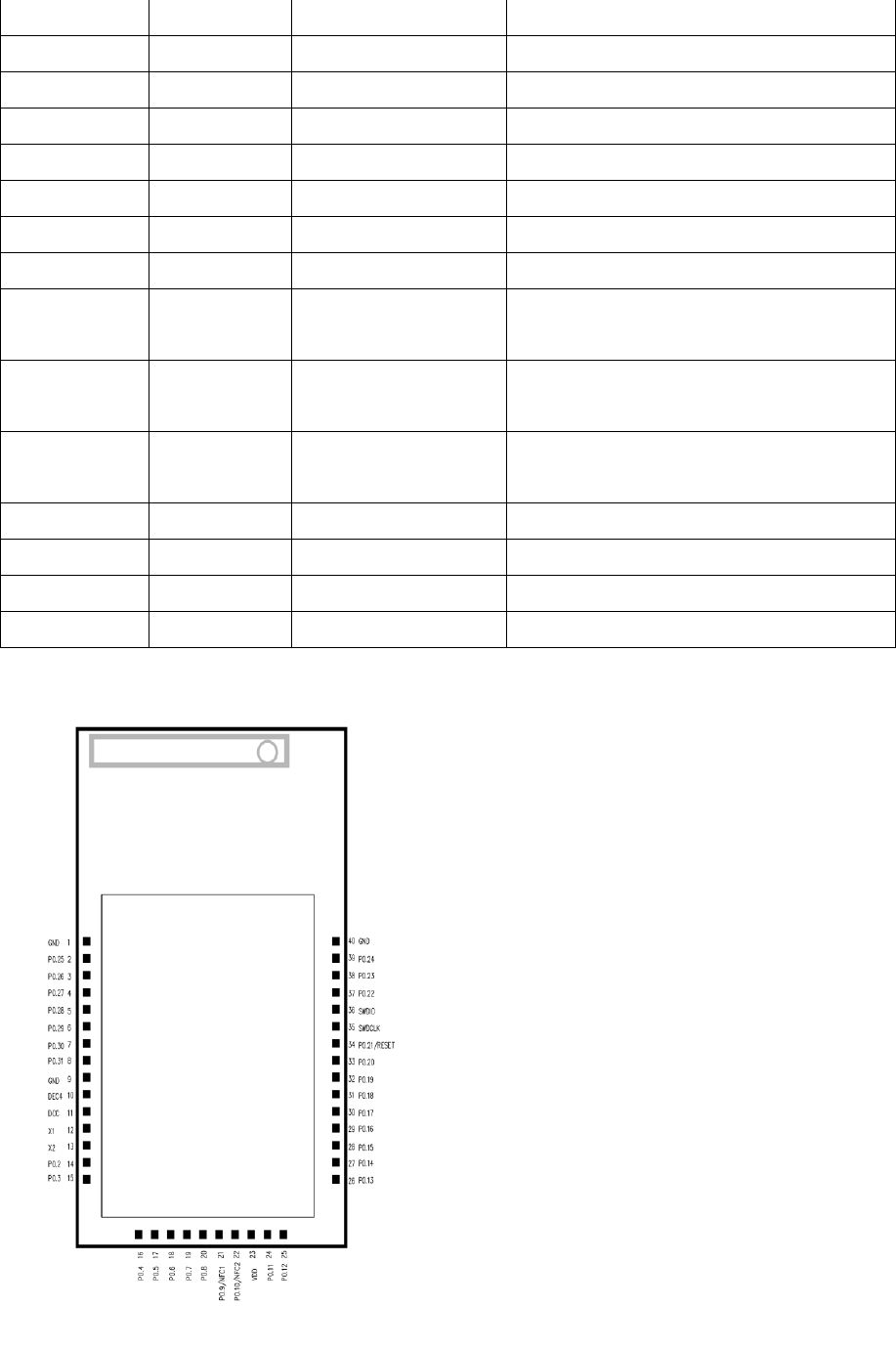
Pin Definitions
Pin number
Pin Name
TYPE
Description
1
GND
POWER
GND PIN
2
P0.25
Digital I/O
General purpose I/O PIN
3
P0.26
Digital I/O
General purpose I/O PIN
4
P0.27
Digital I/O
General purpose I/O PIN
5
P0.28
AIN4
Digital I/O
Analog input
General purpose I/O PIN
SAADC/COMP/LPCOMP input
6
P0.29
AIN5
Digital I/O
Analog input
General purpose I/O PIN
SAADC/COMP/LPCOMP input
7
P0.30
AIN6
Digital I/O
Analog input
General purpose I/O PIN
SAADC/COMP/LPCOMP input
8
P0.31
AIN7
Digital I/O
Analog input
General purpose I/O PIN
SAADC/COMP/LPCOMP input
9
GND
POWER
GND PIN
10
DEC4
NC
11
DCC
NC
12
X1
NC
13
X2
NC
14
P0.2
AIN0
Digital I/O
Analog input
General purpose I/O PIN
SAADC/COMP/LPCOMP input
15
P0.3
AIN1
Digital I/O
Analog input
General purpose I/O PIN
SAADC/COMP/LPCOMP input
16
P0.4
AIN2
Digital I/O
Analog input
General purpose I/O PIN
SAADC/COMP/LPCOMP input
17
P0.5
AIN3
Digital I/O
Analog input
General purpose I/O PIN
SAADC/COMP/LPCOMP input
18
P0.6
Digital I/O
General purpose I/O PIN
19
P0.7
Digital I/O
General purpose I/O PIN
20
P0.8
Digital I/O
General purpose I/O PIN
21
P0.9
NFC1
Digital I/O
NFC INPUT
General purpose I/O PIN
NFC antenna connection
22
P0.10
NFC2
Digital I/O
NFC INPUT
General purpose I/O PIN
NFC antenna connection
23
VDD
POWER
POWER supply pin
24
P0.11
Digital I/O
General purpose I/O PIN
25
P0.12
Digital I/O
General purpose I/O PIN

26
P0.13
Digital I/O
General purpose I/O PIN
27
P0.14
Digital I/O
General purpose I/O PIN
28
P0.15
Digital I/O
General purpose I/O PIN
29
P0.16
Digital I/O
General purpose I/O PIN
30
P0.17
Digital I/O
General purpose I/O PIN
31
P0.18
Digital I/O
General purpose I/O PIN
32
P0.19
Digital I/O
General purpose I/O PIN
33
P0.20
Digital I/O
General purpose I/O PIN
34
P021
RESET
Digital I/O
General purpose I/O PIN
configurable as pin reset
35
SWDCLK
Digital input
serial wire Debug clock input for
debug and programming
36
SWDIO
Digital I/O
serial wire Debug I/O for debug
and programming
37
P0.22
Digital I/O
General purpose I/O PIN
38
P0.23
Digital I/O
General purpose I/O PIN
39
P0.24
Digital I/O
General purpose I/O PIN
40
GND
POWER
GND PIN

This device is intended only for OEM integrators under the following
conditions:
In accordance with FCC Part 15C and RSP-100, this module is listed as a Modular
Transmitter device.
Changes or modifications not expressly approved by the manufacturer could void the user’s
authority to operate the equipment.
The antenna of this transmitter must not be co-located or operating in conjunction with any
other antenna or transmitters within a host device, except in accordance with FCC multi-
transmitter product approval procedures.
FCC Label Instructions
The final end product must be labeled in a visible area with the following “Contains
Transmitter Module FCC ID: QSWDZRCS1”
Any similar wording that expresses the same meaning may be used.
Additionally, there must be the following sentence on the device, unless it is too small to carry
it:
“This device complies with part 15 of the FCC Rules. Operation is subject to the following two
conditions:
(1) This device may not cause harmful interference, and (2) this device must accept any
interference received, including interference that may cause undesired operation.”
USER MANUAL
Changes or modifications not expressly approved by the party responsible for
compliance could void the user’s authority to operate the equipment.