dresden elektronik ingenieurtechnik 23SXX 2.4GHz IEEE 802.15.4 compliant radio module User Manual deRFsamR21E 23S00 23S20
dresden elektronik ingenieurtechnik gmbh 2.4GHz IEEE 802.15.4 compliant radio module deRFsamR21E 23S00 23S20
UserManual.wiki
>
dresden elektronik ingenieurtechnik
>
23SXX User Manual
User man
Navigation menu
Upload a User Manual
Namespaces
Wiki Guide
HTML
PDF
Info
Views
User Manual
Discussion / Help
Navigation
![datasheet Version 0.9 2017-09-13 deRFsamR21E-23S00/-23S20 datasheet www.dresden-elektronik.de Page 5 of 36 Abbreviations Abbreviation Description IEEE 802.15.4 Communication standard, applicable to low-rate Wireless Personal Area Networks (WPAN) 6LoWPAN IPv6 over Low Power Wireless Personal Area Networks ADC Analog to Digital Converter ASF Atmel Software Framework EMI Electromagnetic Interference ETSI European Telecommunications Standards Institute FCC Federal Communications Commission GPIO Generals Purpose Input Output LNA Low Noise Amplifier MAC Medium (Media) Access Control MCU, µC Microcontroller Unit OTAU Over the air update PA Power Amplifier PCB Printed Circuit Board PWM Pulse Width Modulation RED Radio Equipment Directive RF Radio Frequency R&TTE Radio and Telecommunications Terminal Equipment (Directive of the European Union) SoC System On Chip SPI Serial Peripheral Interface SWD Serial Wire Debug TWI Two-Wire Serial Interface U[S]ART Universal [Synchronous/]Asynchronous Receiver Transmitter USB Universal Serial Bus ZigBee Low-cost, low-power wireless mesh network standard. The ZigBee Alliance is a group of companies that maintain and publish the ZigBee standard.](https://usermanual.wiki/dresden-elektronik-ingenieurtechnik/23SXX/User-Guide-3575098-Page-5.png)
![datasheet Version 0.9 2017-09-13 deRFsamR21E-23S00/-23S20 datasheet www.dresden-elektronik.de Page 9 of 36 4. Pinout In this chapter the pinout is described. The following figure shows the pinout of the radio module. The pinout applies to both variants 23S00 and 23S20. Top-View 1 GND 2 NC/RF-OUT1 3 GND 4 GND 27 GND 5 PA14 26 PA09 6 PA15 25 PA08 7 PA16/MISO2 24 PA06 8 PA17/CLK2 23 PA07 9 PA18/SS2 22 GND 10 PA19/MOSI2 21 RESET 11 PA24 20 PA31 12 PA25 19 PA30 13 VCC 18 PA28 14 VCC 17 PA27 15 GND 16 GND 1. RF-OUT only for deRFsamR21E-23S20, do not connect for deRFsamR21E-23S00 and if unused. 2. The onboard data flash is connected to the controller at these pins. The SPI chip-select (SS signal) is not available for use other than internal data flash control. For a recommended configuration of the module pins with all common interfaces see Section 10. A more detailed description on port to function assignment can be found in [1] Table 5-1.](https://usermanual.wiki/dresden-elektronik-ingenieurtechnik/23SXX/User-Guide-3575098-Page-9.png)
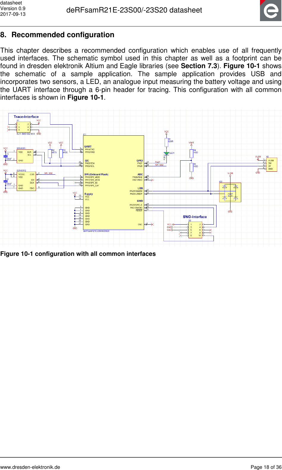
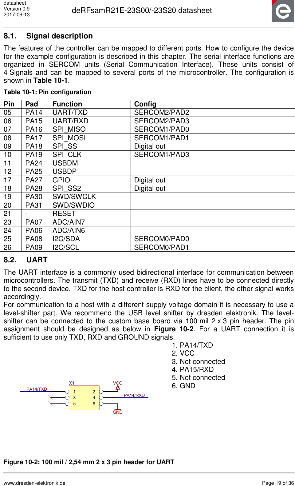
![datasheet Version 0.9 2017-09-13 deRFsamR21E-23S00/-23S20 datasheet www.dresden-elektronik.de Page 12 of 36 Figure 7-3: Recommended Footprint for deRFsamR21E-23S20 The recommended pad size is 0.9 x 1.4 mm, solder mask clearance is 75 to 100 µm, stencil opening is 0.8 x 1.25 mm with stencil thickness 100 to 150 µm. The 23S00 with internal antenna requires the user to follow the placement and layout guidelines for best RF performance. For more details see Section 11.6 and 11.7. With the RF-pad of 23S20 it is possible to implement antenna diversity and front-end design for increased transmit power and receiver sensitivity as well as custom antenna design. More details can be found in chapter 11.8.1 External front end and antenna diversity. 5.3. ECAD libraries dresden elektronik offers schematic and footprint libraries for all available radio modules for ECAD design software Altium Designer® [3] and Eagle® [5]. This allows a fast design-in of radio modules into a custom product. The pin-assignment in the schematic library is a suggestion for frequently used functions. A detailed description on this configuration can be found in Section 10. The pins can be muxed in many different ways with other functions depending on application needs. For more details on that refer to Section 6. 5.4. STEP model library dresden elektronik offers a STEP model library with all available OEM radio modules for CAD design tools [7].](https://usermanual.wiki/dresden-elektronik-ingenieurtechnik/23SXX/User-Guide-3575098-Page-12.png)
![datasheet Version 0.9 2017-09-13 deRFsamR21E-23S00/-23S20 datasheet www.dresden-elektronik.de Page 15 of 36 Table 8-3: TX_PWR Register settings at 3.0V TX_PWR Value TX Output Power [dBm] Current Consuption [mA]1 0x0 4 13.8 0x1 3.7 0x2 3.4 0x3 3 0x4 2.5 0x5 2 0x6 1 0x7 0 11.8 0x8 -1 0x9 -2 0xA -3 0xB -4 0xC -6 0xD -8 0xE -12 0xF -17 7.2 Note: 1. Current consumption for transceiver only, MCU and data flash currents have to be considered as well 6.4. Fuse setting Fuses are used to configure the ATSAMR21E18 operation modes and clocks. This is mainly done by internal commands which can be found in [1].](https://usermanual.wiki/dresden-elektronik-ingenieurtechnik/23SXX/User-Guide-3575098-Page-15.png)
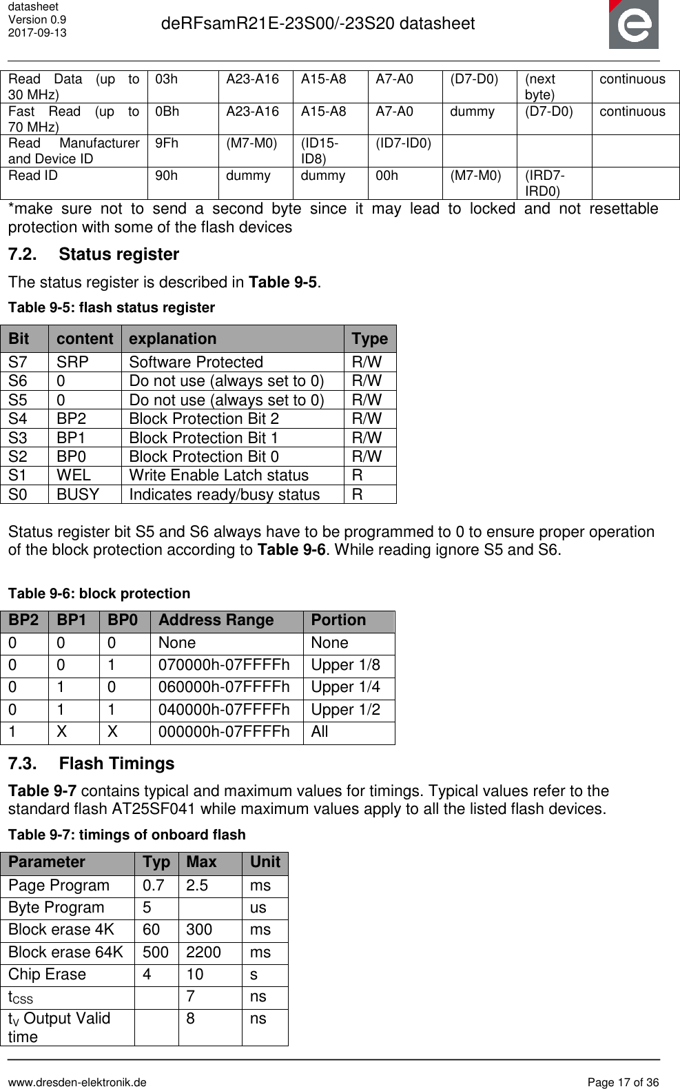
![datasheet Version 0.9 2017-09-13 deRFsamR21E-23S00/-23S20 datasheet www.dresden-elektronik.de Page 16 of 36 7. Onboard SPI Serial Flash The module incorporates a 4 MBit data flash connected to the module by SPI bus. The data flash connects to PA16-PA19 according to Table 9-1. Table 9-1: Dataflash to microcontroller connection Port Function Flash pin Controller settings PA16 MISO SO PA16 SERCOM1 or 3 PAD[0] DIPO=0x0 PA17 SCK SCK PA17 SERCOM1 or 3 PAD[1] DOPO=0x2 PA18 GPIO SS PA18 to be set low in software before SPI access PA19 MOSI SI PA19 SERCOM1 or 3 PAD[3] DOPO=0x2 The signals in this table are available at module pins 7-10 as well. The module contains the serial data flash AT25SF041 according to Table 9-2. Since the memory market is very difficult at the moment, the module incorporates some alternative flash devices listed in Table 9-3. This is done to avoid supply bottlenecks. To avoid problems, no specific flash ID shall be used in the customer firmware. This section outlines basic usage instructions. For a more detailed description refer to the datasheets of the flash devices. Table 9-2: default serial data flash Partnumber Manufacturer JEDEC ID (9Fh) Datasheet reference AT25SF041 Adesto 1F-84-01 [9] Table 9-3: second source serial data flash list Partnumber Manufacturer JEDEC ID (9Fh) Datasheet reference MX25V4006E Macronix C2-20-13 [10] W25X40CL Winbond EF-30-13 [11] W25Q40CL Winbond EF-40-13 [12] 7.1. Commands To ease the implementation of the different flash devices Table 9-4 lists the commands and their respective opcodes common to all the flash devices listed above. Table 9-4: command table common to all flash options Command Opcode Byte 2 Byte 3 Byte 4 Byte 5 Byte 6 Byte n Write enable 06h Write disable 04h Read Status Register 05h (S7-S0) Write Status Register 01h S7-S0 see* Page Program 02h A23-A16 A15-A8 A7-A0 (D7-D0) (next byte) Up to 256 bytes Sector Erase (4kB) 20h A23-A16 A15-A8 A7-A0 Block Erase (64kB) D8h A23-A16 A15-A8 A7-A0 Chip Erase C7h/60h Power-down B9h Resume from Deep Power Down ABh Resume from Deep Power Down and read ID ABh dummy dummy dummy (IRD7-IRD0)](https://usermanual.wiki/dresden-elektronik-ingenieurtechnik/23SXX/User-Guide-3575098-Page-16.png)
![datasheet Version 0.9 2017-09-13 deRFsamR21E-23S00/-23S20 datasheet www.dresden-elektronik.de Page 24 of 36 Board thickness of 1.55 mm Copper layer thickness of 35 µm Top and bottom solder 9.8. RF Design for deRFsamR21E-23S20 For deRFsamR21E-23S20 two options for the RF signal are available: using the coaxial u.FL connector to connect an external antenna or if needed in the application, custom designed RF circuitry using the RF-out pad. Note: Please get in contact with dresden elektronik to advise for a custom FCC certified design. If necessary dresden elektronik can provide RF part design data. This may require signing a Non-Disclosure Agreement. When designing RF traces on the base board a line impedance of 50 Ω shall be used. Depending on the base board layer stack construction a microstrip or grounded coplanar microstrip design can be implemented. 9.8.1. External front end and antenna diversity The radio module deRFsamR21E-23S20 can be used with an external front end, including power amplifier (PA) for transmission and low noise amplifier (LNA) for receiving, and antenna diversity. Figure 11-8 shows a possible design as block diagram. A custom design can contain a single PA or single LNA or a complete integrated front-end chip. It depends mainly on the application. Furthermore, it is possible to include a RF switch for driving the antenna diversity feature. An example block diagram is shown in Figure 11-8. Figure 11-8: block diagram for external PA/LNA and antenna diversity control The DIG1 to DIG4 signals of the transceiver are connected internally to the microcontroller and have to be muxed on ports PA08, PA09, PA14 and PA15. DIG1 to DIG4 can be activated as alternate pin output functions FECTRL[0..5] by the microcontroller. Please refer to chapter 33 of ATSAMR21 datasheet [1]. Unbalanced RF output The radio module deRFsamR21E-23S20 has a 50 Ω unbalanced RF output. For designs with external RF power amplifier a RF switch is required to separate the TX and RX path.](https://usermanual.wiki/dresden-elektronik-ingenieurtechnik/23SXX/User-Guide-3575098-Page-24.png)
![datasheet Version 0.9 2017-09-13 deRFsamR21E-23S00/-23S20 datasheet www.dresden-elektronik.de Page 26 of 36 10. Programming The update process of the radio module, the required software and hardware for programming via SWD interface and the driver installation on different operating systems are described in this chapter. Currently, the SWD interface is supported by several Atmel and third party programmers and debuggers like Atmel ICE and Segger J-Link. Other programmers that support ATSAMR21E18A will work as well. For the programming the standard SWD header is recommended as 10pin 1.27 mm header as shown in Figure 12-1. Figure 12-1: Programming header 10.1. Software/Applications For software development several options are available depending on your needs: For low-cost embedded wireless applications the MiWi Stack from Microchip supports the ATSAMR21. More information can be found at http://www.microchip.com/design-centers/wireless-connectivity/embedded-wireless/802-15-4/software/miwi-protocol For ZigBee 3.0 home automation projects Microchip offers the ZigBee 3.0 BitCloud software stack. This stack is platform certified by the ZigBee Alliance. For more information see http://www.microchip.com/design-centers/wireless-connectivity/embedded-wireless/802-15-4/zigbee-3-0 Please contact your local Microchip Sales Representative to get access to the BitCloud Software Development Kit. In Atmel Studio the Atmel Software Framework (ASF) offers a big number of examples for ATSAMR21G18A. It is the same controller in a package with more GPIO Pins available for the user. Some minor adjustments are necessary to allow the examples to run on ATSAMR21E18A on this module. Suitable compilers are GCC (v4.5.2) or IAR Compiler(IAR C/C++ Compiler for ARM v7.80.1) for example. Dresden elektronik offers software development services for with comprehensive experience in ZigBee 3.0 and IEEE 802.15.4 wireless applications. 10.2. Clocks The controller runs on 8 MHz RC-oscillator by default. Since the internal clock generation is not very accurate, it is recommended to use the external transceiver oscillator to avoid problems during communication for example by UART. To change the clock source to the precise transceiver oscillator (±10 ppm at 25°C) the transceiver has to be configured for clock output (CLKM) and the clock source at the controller has to be set to „GLCKIN“/“ GCLK_IO[1]“. During deep sleep operation the clock source is best set to „OSCULP32K“ for minimized current consumption. Further information can be found in [1].](https://usermanual.wiki/dresden-elektronik-ingenieurtechnik/23SXX/User-Guide-3575098-Page-26.png)
![datasheet Version 0.9 2017-09-13 deRFsamR21E-23S00/-23S20 datasheet www.dresden-elektronik.de Page 29 of 36 11.2. European Union (ETSI) Hereby, dresden elektronik ingenieurtechnik gmbh declares that the radio equipment types deRFsamR21E-23S00 and deRFsamR21E-23S20 are in compliance with the Directive 2014/53/EU. The full text of the EU declaration of conformity is available at the following internet address: https://www.dresden-elektronik.de/funktechnik/solutions/wireless-light-control/eu-conformity/?L=1. If the deRFsamR21E-23S00 and deRFsamR21E-23S20 modules are incorporated into a product, the manufacturer must ensure compliance of the final product to the European harmonized EMC and low-voltage/safety standards. A Declaration of Conformity must be issued for each of these standards and kept on file as described in Annex VI of the Radio Equipment Directive 2014/53/EU. The manufacturer must maintain a copy of the deRFsamR21E-23S00 and deRFsamR21E-23S20 modules documentation and ensure the final product does not exceed the specified power ratings, antenna specifications, and/or installation requirements as specified in the user manual. If any of these specifications are exceeded in the final product, a submission must be made to a notified body for compliance testing to all required standards. The CE marking must be affixed to a visible location on the OEM product. The CE mark shall consist of the initials "CE" taking the following form: If the CE marking is reduced or enlarged, the proportions must be respected. The CE marking must have a height of at least 5 mm except where this is not possible on account of the nature of the apparatus. The CE marking must be affixed visibly, legibly, and indelibly. More detailed information about CE marking requirements can be found in [3].](https://usermanual.wiki/dresden-elektronik-ingenieurtechnik/23SXX/User-Guide-3575098-Page-29.png)
![datasheet Version 0.9 2017-09-13 deRFsamR21E-23S00/-23S20 datasheet www.dresden-elektronik.de Page 30 of 36 11.3. Approved antennas The deRFsamR21E-23S00 has an integrated chip antenna. The design is fully compliant with all regulations. The deRFsamR21E-23S20 is compliant with the listed approved antennas in Table 13-1. Table 13-1: Approved antenna(s) and accessory Approved antenna list Type Gain Mount Order code Vendor / Supplier External antenna 2400 to 2483.5 MHz Rubber antenna +5dBi (peak) RP-SMA 17013.RSMA WiMo U.FL-to-RP-SMA pigtail, 15 cm -0.5dB BN-023769 dresden elektronik Integrated antenna 2400 to 2483.5 MHz Chip antenna +0.5dBi (peak) SMT AMCA31-2R450G-S1F-T Abracon LLC According to FCC KDB 178919 [5] it is allowed to substitute approved antennas through equivalent antennas of the same type with equal or less antenna gain: ‘Equivalent antennas must be of the same type (e.g., yagi, dish, etc.), must be of equal or less gain than an antenna previously authorized under the same FCC ID, and must have similar in band and out-of-band characteristics (consult specification sheet for cutoff frequencies).’](https://usermanual.wiki/dresden-elektronik-ingenieurtechnik/23SXX/User-Guide-3575098-Page-30.png)
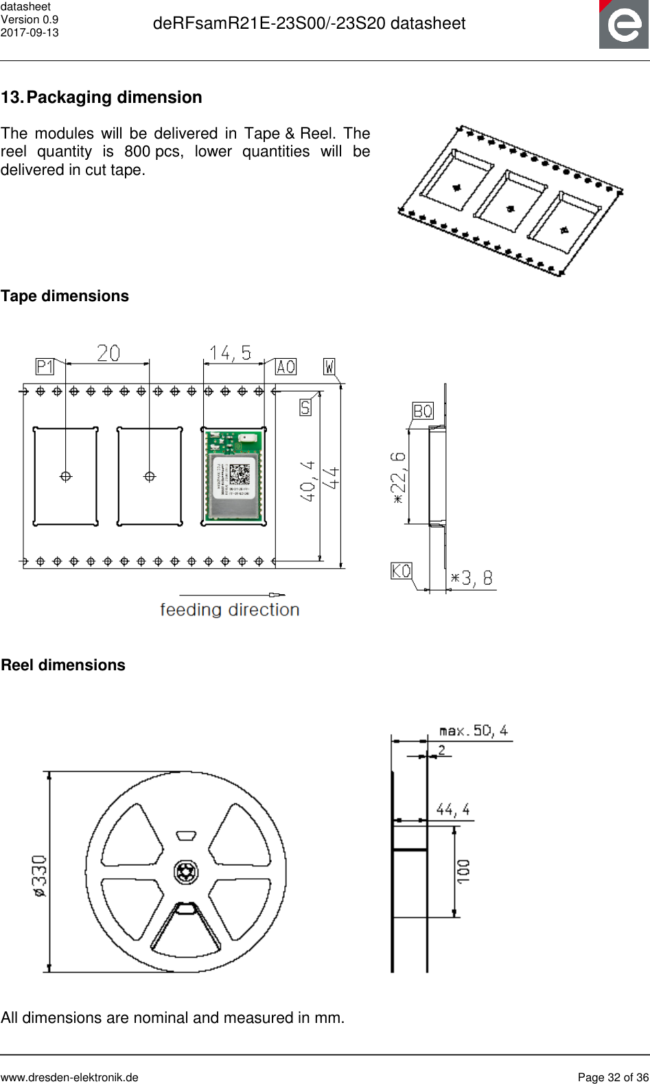
![datasheet Version 0.9 2017-09-13 deRFsamR21E-23S00/-23S20 datasheet www.dresden-elektronik.de Page 33 of 36 14. Soldering profile Table 16-1 shows the recommended soldering profile for the radio modules. Table 16-1: Soldering Profile Profile Feature Values Average-Ramp-up Rate (217°C to Peak) 3°C/s max Preheat Temperature 175°C ±25°C 180 s max Temperature Maintained Above 217°C 60 s to 150 s Time within 5°C of Actual Peak Temperature 20 s to 40 s Peak Temperature Range 260°C Ramp-down Rate 6°C/s max Time 25°C to Peak Temperature 8 min max Figure 16-1 shows a recorded soldering profile for a radio module. The blue colored line illustrates a temperature sensor placed next to the soldering contacts of the radio module. The pink line shows the set temperatures depending on the zone within the reflow soldering machine. Figure 16-1: Recorded soldering profile A solder process without supply of nitrogen causes a discoloration of the metal RF-shielding. It is possible that the placed label shrinks due the reflow process. 406080100120140160180200220240260280020406080100120140160180200220240260280300320340360T [°C] t [s] Measured Temp. Zone Temp.](https://usermanual.wiki/dresden-elektronik-ingenieurtechnik/23SXX/User-Guide-3575098-Page-33.png)
![datasheet Version 0.9 2017-09-13 deRFsamR21E-23S00/-23S20 datasheet www.dresden-elektronik.de Page 34 of 36 15. Revision notes Actually, no design issues of the radio modules are known. All errata of the ATSAMR21E18A are described in the datasheet [1].](https://usermanual.wiki/dresden-elektronik-ingenieurtechnik/23SXX/User-Guide-3575098-Page-34.png)
![datasheet Version 0.9 2017-09-13 deRFsamR21E-23S00/-23S20 datasheet www.dresden-elektronik.de Page 35 of 36 16. References [1] ATSAMR21E18A: Atmel SAM R21E / SAM R21G, SMART ARM-Based Wireless Microcontroller; Datasheet, URL: http://www.microchip.com/wwwproducts/en/ATSAMR21E18A [2] AT86RF233: Low Power, 2.4GHz Transceiver for ZigBee, RF4CE, IEEE 802.15.4, 6LoWPAN, and ISM Applications; Datasheet, URL: http://www.microchip.com/wwwproducts/en/at86rf233 [3] Directive 2014/53/EU, European Parliament and the Council, 16 April 2014, URL: http://eur-lex.europa.eu/legal-content/en/ALL/?uri=CELEX:32014L0053 [4] Transmitter Module Equipment Authorization Guide; 996369 D01 Module Certification Guide; FCC OET; URL: https://apps.fcc.gov/oetcf/kdb/forms/FTSSearchResultPage.cfm?id=44637&switch=P [5] Permissive Change Policy; 178919 D01 Permissive Change Policy; FCC OET; URL: https://apps.fcc.gov/oetcf/kdb/forms/FTSSearchResultPage.cfm?id=33013&switch=P [6] 2.4GHz Chip-Antenna AMCA31-2R450G-S1F-T by Abracon LLC; Datasheet; URL: http://www.abracon.com/chip-antenna/AMCA31-2R450G-S1F-T.pdf [7] 2.4GHz Rubber antenna 17013.xx by WiMo Antennen und Elektronik GmbH; Datasheet; URL: http://www.wimo.com/download/17013.pdf [8] Schematic and footprint library for Altium Designer®; URL: http://www.dresden-elektronik.de/funktechnik/service/downloads/documentation/?eID=dam_frontend_push&docID=2024 [9] Schematic and footprint library for EAGLE®; URL: http://www.dresden-elektronik.de/funktechnik/service/downloads/documentation/?eID=dam_frontend_push&docID=2023 [10] STEP model library for CAD tools; URL: http://www.dresden-elektronik.de/funktechnik/service/downloads/documentation/?eID=dam_frontend_push&docID=2022 [11] Link Config file Atmel Start [12] Flash AT25SF041 by Adesto; Datasheet; URL: https://www.adestotech.com/wp-content/uploads/DS-AT25SF041_044.pdf [13] Flash MX25V4006E by Macronix; Datasheet; URL: http://www.macronix.com/Lists/Datasheet/Attachments/6217/MX25V4006E,%202.5V,%204Mb,%20v1.9.pdf [14] Flash W25X40CL by Winbond; Datasheet; URL: http://www.winbond.com/resource-files/w25x40cl_f%2020140325.pdf [15] Flash W25X40CL by Winbond; Datasheet; URL: http://www.winbond.com/resource-files/da00-w25q40cle1.pdf](https://usermanual.wiki/dresden-elektronik-ingenieurtechnik/23SXX/User-Guide-3575098-Page-35.png)