dresden elektronik ingenieurtechnik 23SXX 2.4GHz IEEE 802.15.4 compliant radio module User Manual deRFsamR21E 23S00 23S20
dresden elektronik ingenieurtechnik gmbh 2.4GHz IEEE 802.15.4 compliant radio module deRFsamR21E 23S00 23S20
User man
deRFsamR21E
-23S00/-23S20
Datasheet
1. General description
The deRFsamR21E is a 2.4GHz ZigBee 3.0 radio module
series which integrates the SoC ATSAMR21E18 from
Microchip / Atmel together with a 4 Mbit data flash on a tiny
size of 21 mm x 13 mm. The microcontroller ATSAMR21E18
integrates a powerful and energy efficient 32-Bit ARM Cortex-
M0+ core together with a 2.4 GHz ZigBee radio transceiver.
The module comes with 16 I/O’s, 256 kbit internal program
flash and 4 Mbit data flash for firmware updates over the air
and data storage. For reliable assembly the module offers
SMD solderable side contacts in 50 mil / 1.27 mm grid. The
module offers ZigBee 3.0 support for smart devices.
Two radio module variants are available:
deRFsamR21E-23S00: integrated RF-design with
chip antenna
deRFsamR21E-23S20: coaxial u.FL-connector for
external antenna applications as well as a RF-pad for
custom RF-designs e.g. external frontend or antenna
diversity
deRFsamR21E-23S00
deRFsamR21E-23S20
2. Features
ATSAMR21E18 Single-chip ARM Cortex-M0+ based 32-bit Microcontroller with Low
Power 2.4 GHz Transceiver for IEEE 802.15.4 and ZigBee Applications with 256 KB
Flash and 16 I/O’s - all accessible outside the module (four occupied by data flash)
- Maximum operating frequency 48 MHz
- 128-bit AES crypto engine
- 32-bit MAC symbol counter
- Temperature sensor
- Automatic transmission modes
4 Mbit data flash for firmware updates over the air and data storage
Ready-to-use RF design
Radio module with a link budget of up to 103 dBm
CE compliant according to RED 2014/53/EU and FCC certified
Single 2.5 V - 3.6 V supply
Industrial temperature range -40°C to 85°C
1.27 mm / 50 mil pin header with several alternative functions:
- Analog input (12-bit, 350ksps Analog-to-Digital Converter)
- PWM output
- TWI (I2C up to 3.4MHz)
- SPI
- UART
- USB
- GPIO
- SWD programming interface
High precision 16 MHz crystal oscillator

datasheet
Version 0.9
2017-09-13
deRFsamR21E-23S00/-23S20 datasheet
www.dresden-elektronik.de
Page 2 of 36
Table of contents
1. General description ......................................................................................................... 1
2. Features .......................................................................................................................... 1
1. Overview ......................................................................................................................... 6
2. Applications ..................................................................................................................... 6
3. Block diagram .................................................................................................................. 7
4. Pinout .............................................................................................................................. 9
5. Mechanical description .................................................................................................. 10
5.1. Module dimensions............................................................................................... 10
5.2. Recommended footprint ....................................................................................... 11
5.3. ECAD libraries ...................................................................................................... 12
5.4. STEP model library............................................................................................... 12
6. Electrical specification ................................................................................................... 13
6.1. Absolute Maximum Ratings .................................................................................. 13
6.2. Electrical Characteristics ...................................................................................... 13
6.3. TX Power register settings .................................................................................... 14
6.4. Fuse setting .......................................................................................................... 15
7. Onboard SPI Serial Flash .............................................................................................. 16
7.1. Commands ........................................................................................................... 16
7.2. Status register ...................................................................................................... 17
7.3. Flash Timings ....................................................................................................... 17
8. Recommended configuration ......................................................................................... 18
8.1. Signal description ................................................................................................. 19
8.2. UART ................................................................................................................... 19
8.3. I2C (TWI) .............................................................................................................. 20
8.4. USB ...................................................................................................................... 20
8.5. SPI ....................................................................................................................... 20
8.6. ADC ..................................................................................................................... 20
8.7. SWD ..................................................................................................................... 20
8.8. GPIO .................................................................................................................... 20
8.9. Reset .................................................................................................................... 20
9. Application Information .................................................................................................. 21
9.1. PCB Technology .................................................................................................. 21
9.2. Power supply ........................................................................................................ 21
9.3. Ground plane........................................................................................................ 21
9.4. Layers .................................................................................................................. 21
9.5. Traces below the module...................................................................................... 22
9.6. Placement on the PCB ......................................................................................... 22
9.7. Recommended layout for deRFsamR21E-23S00 ................................................. 23
9.8. RF Design for deRFsamR21E-23S20 ................................................................... 24
9.8.1. External front end and antenna diversity ................................................... 24

datasheet
Version 0.9
2017-09-13
deRFsamR21E-23S00/-23S20 datasheet
www.dresden-elektronik.de
Page 3 of 36
10. Programming ................................................................................................................. 26
10.1. Software/Applications ........................................................................................... 26
10.2. Clocks .................................................................................................................. 26
10.3. Pre-flashed firmware ............................................................................................ 27
11. Radio certification .......................................................................................................... 28
11.1. United States (FCC) ............................................................................................. 28
11.2. European Union (ETSI) ........................................................................................ 29
11.3. Approved antennas .............................................................................................. 30
12. Ordering information ...................................................................................................... 31
13. Packaging dimension .................................................................................................... 32
14. Soldering profile............................................................................................................. 33
15. Revision notes ............................................................................................................... 34
16. References .................................................................................................................... 35

datasheet
Version 0.9
2017-09-13
deRFsamR21E-23S00/-23S20 datasheet
www.dresden-elektronik.de
Page 4 of 36
Document history
Date
Version
Description
2017-09-13
0.9
Preliminary version
datasheet
Version 0.9
2017-09-13
deRFsamR21E-23S00/-23S20 datasheet
www.dresden-elektronik.de
Page 5 of 36
Abbreviations
Abbreviation
Description
IEEE 802.15.4
Communication standard, applicable to low-rate Wireless Personal Area
Networks (WPAN)
6LoWPAN
IPv6 over Low Power Wireless Personal Area Networks
ADC
Analog to Digital Converter
ASF
Atmel Software Framework
EMI
Electromagnetic Interference
ETSI
European Telecommunications Standards Institute
FCC
Federal Communications Commission
GPIO
Generals Purpose Input Output
LNA
Low Noise Amplifier
MAC
Medium (Media) Access Control
MCU, µC
Microcontroller Unit
OTAU
Over the air update
PA
Power Amplifier
PCB
Printed Circuit Board
PWM
Pulse Width Modulation
RED
Radio Equipment Directive
RF
Radio Frequency
R&TTE
Radio and Telecommunications Terminal Equipment
(Directive of the European Union)
SoC
System On Chip
SPI
Serial Peripheral Interface
SWD
Serial Wire Debug
TWI
Two-Wire Serial Interface
U[S]ART
Universal [Synchronous/]Asynchronous Receiver Transmitter
USB
Universal Serial Bus
ZigBee
Low-cost, low-power wireless mesh network standard. The ZigBee Alliance
is a group of companies that maintain and publish the ZigBee standard.

datasheet
Version 0.9
2017-09-13
deRFsamR21E-23S00/-23S20 datasheet
www.dresden-elektronik.de
Page 6 of 36
1. Overview
The deRFsamR21E series is the second generation of small, ready-to-use radio modules that
provides a fully integrated solution for wireless applications, using the IEEE802.15.4 standard in
the 2.45 GHz ISM frequency band. All required RF components are already integrated on the
module, therefore no expensive RF design is needed. Features can be added by simply connect-
ing sensors and output stages to the module. The deRFsamR21E module series reduces time to
market, effort and cost significantly for wireless applications.
The deRFsamR21E series is based on the SoC ATSAMR21E18 from Microchip/ Atmel which
features an ARM Cortex-M0+ core and a 2.4 GHz ZigBee transceiver. It enables use of ZigBee
3.0 for smart devices in a wide field of applications. For this tiny series, dresden elektronik is us-
ing a footprint, which offers SMD solderable side contacts in a 50 mil / 1.27 mm grid for easy
assembly and inspection. The module offers 256 KB internal flash as program memory as well
as 4 Mbit data flash for firmware updates over the air and data storage.
Two radio module variants are available:
deRFsamR21E-23S00: integrated RF-design with chip antenna for easy and fast
integration with no need for custom RF design and low BOM cost since all necessary
components are integrated on the module
deRFsamR21E-23S20: coaxial u.FL-connector for external antenna applications as
well as a RF-pad which enables custom RF-design e.g. use of external frontend with
power amplifier/ low noise amplifier or antenna diversity
Both modules are full compliant to all EU and FCC regulatory requirements.
2. Applications
The main applications for the radio modules are:
ZigBee 3.0
Smart Home
Lighting Application
Home Automation
Wireless Sensor Networks
Industrial Controlling
Smart Metering
6LoWPAN
datasheet
Version 0.9
2017-09-13
deRFsamR21E-23S00/-23S20 datasheet
www.dresden-elektronik.de
Page 7 of 36
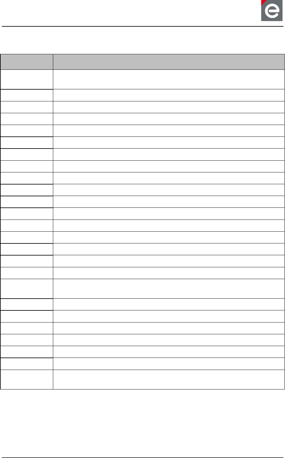
3. Block diagram
Figure 5-15 shows the block diagram of the radio module deRFsamR21E-23S00.
ATSAMR21E18
4Mbit Serial Flash Balun &
Harmonic
Filter
Chip
Antenna
SPI
12 GPIO
SPI
VCC
Figure 3-1: Block diagram deRFsamR21E-23S00
Figure 5-2 shows the block diagram of the radio module deRFsamR21E-23S20 with u.FL
connector.
ATSAMR21E18 Balun &
Harmonic
Filter
12 GPIO
U.FL
4Mbit Serial Flash SPI
SPI
VCC
Figure 5-2: Block diagram deRFsamR21E-23S20
datasheet
Version 0.9
2017-09-13
deRFsamR21E-23S00/-23S20 datasheet
www.dresden-elektronik.de
Page 8 of 36
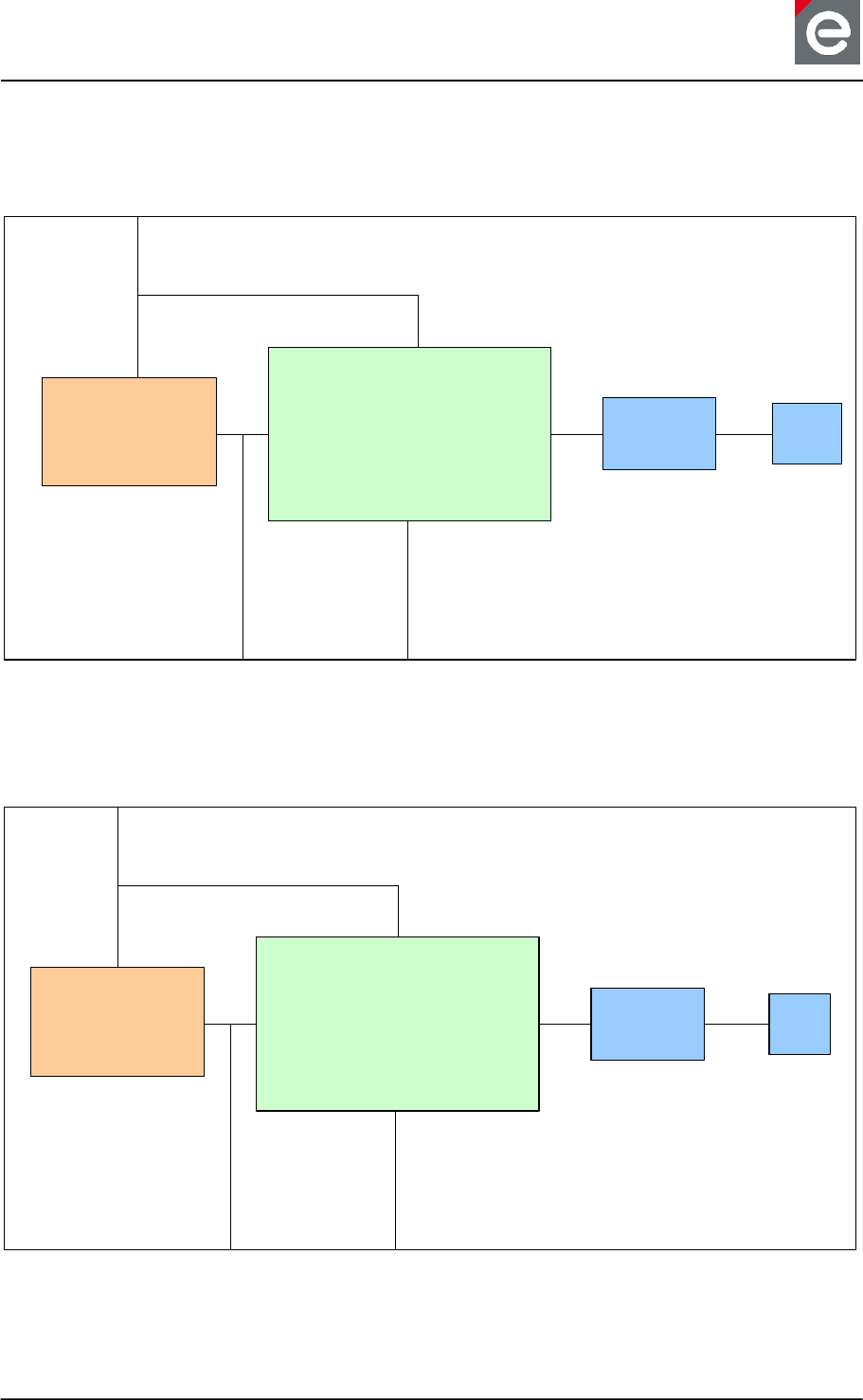
Figure 5-3 shows the block diagram of the radio module deRFsamR21E-23S20 with RF-out
pad.
ATSAMR21E18 Balun &
Harmonic
Filter
12 GPIO
4Mbit Serial Flash SPI
SPI
VCC
RF-out
Figure 5-3: Block diagram deRFsamR21E-23S20 with RF-out pad used
datasheet
Version 0.9
2017-09-13
deRFsamR21E-23S00/-23S20 datasheet
www.dresden-elektronik.de
Page 9 of 36
4. Pinout
In this chapter the pinout is described. The following figure shows the pinout of the radio
module. The pinout applies to both variants 23S00 and 23S20.
Top-View
1
GND
2
NC/RF-OUT1
3
GND
4
GND
27
GND
5
PA14
26
PA09
6
PA15
25
PA08
7
PA16/MISO2
24
PA06
8
PA17/CLK2
23
PA07
9
PA18/SS2
22
GND
10
PA19/MOSI2
21
RESET
11
PA24
20
PA31
12
PA25
19
PA30
13
VCC
18
PA28
14
VCC
17
PA27
15
GND
16
GND
1. RF-OUT only for deRFsamR21E-23S20, do not connect for deRFsamR21E-23S00
and if unused.
2. The onboard data flash is connected to the controller at these pins. The SPI chip-
select (SS signal) is not available for use other than internal data flash control.
For a recommended configuration of the module pins with all common interfaces see
Section 10. A more detailed description on port to function assignment can be found in [1]
Table 5-1.
datasheet
Version 0.9
2017-09-13
deRFsamR21E-23S00/-23S20 datasheet
www.dresden-elektronik.de
Page 10 of 36
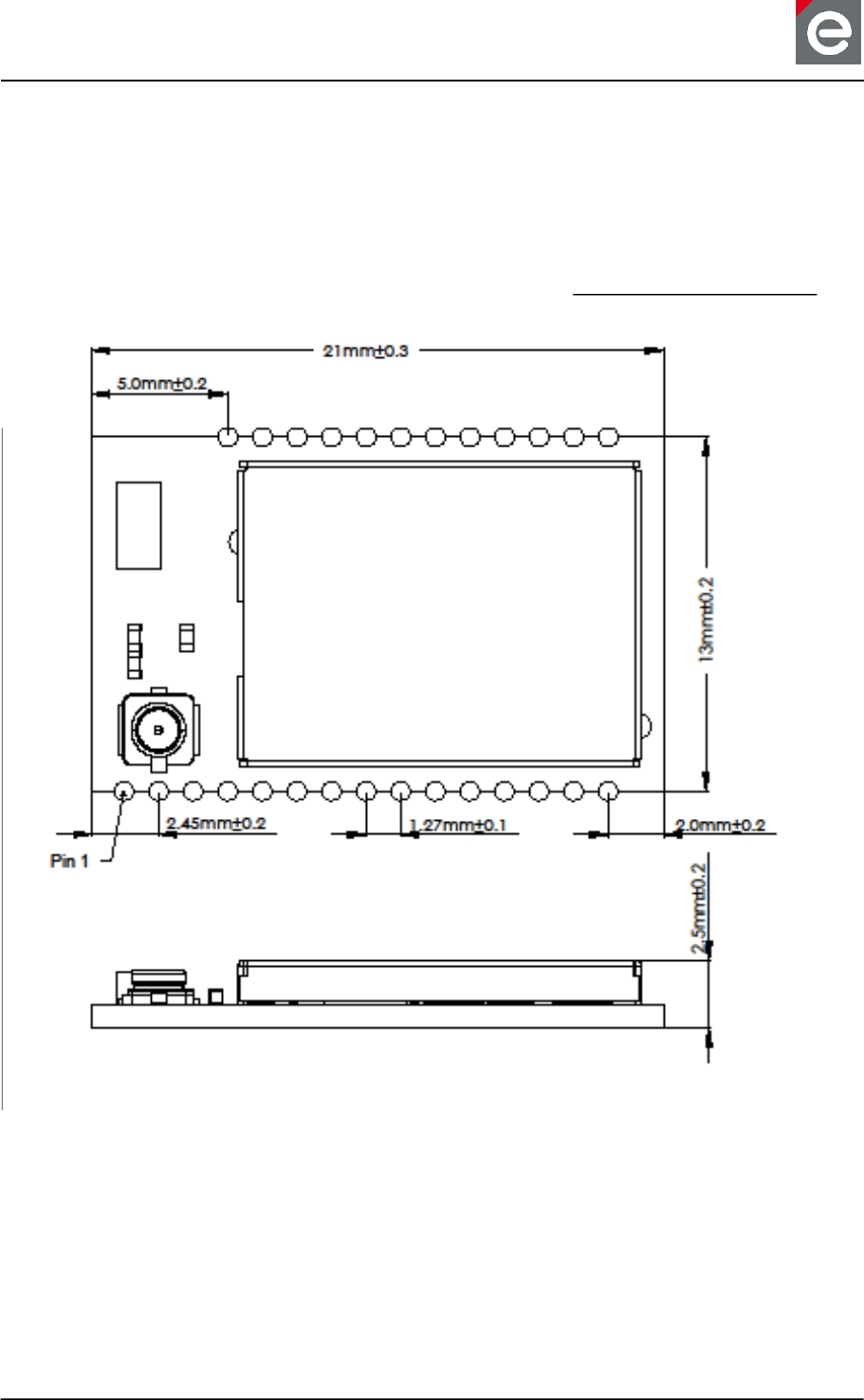
5. Mechanical description
5.1. Module dimensions
The mechanical dimensions are described in this chapter. The modules size is
21.0 x 13.0 x 2.5 mm (0,827 x 0,512 x 0,098 inch). Figure 7-1 shows additional dimensions.
Figure 7-1: mechanical dimensions of the module
datasheet
Version 0.9
2017-09-13
deRFsamR21E-23S00/-23S20 datasheet
www.dresden-elektronik.de
Page 11 of 36
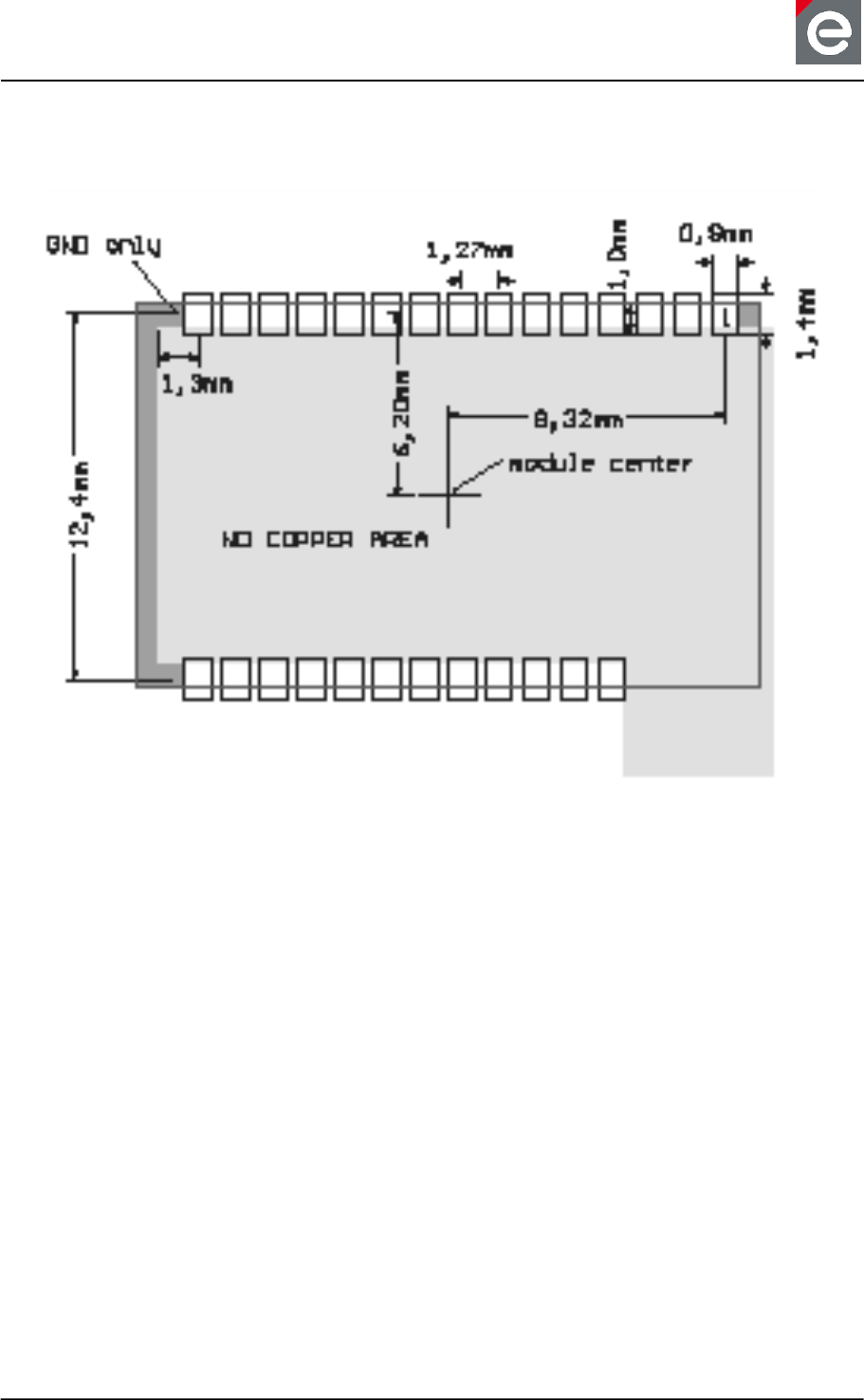
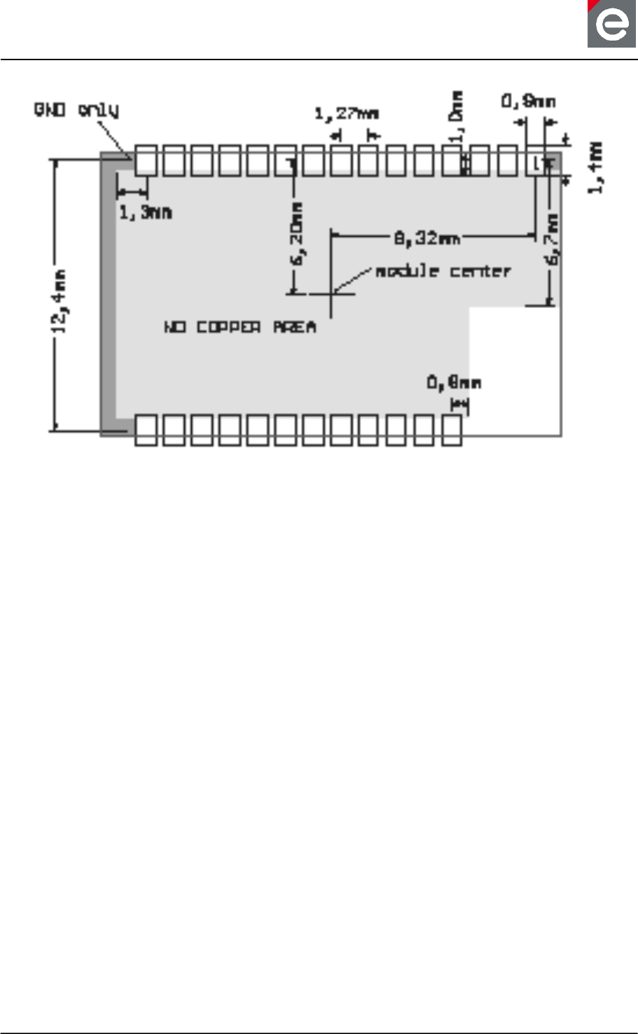
5.2. Recommended footprint
Both radio module types share the same footprint, only the area which it is not allowed to
place copper on is different.
Figure 7-2: Recommended Footprint for deRFsamR21E-23S00
datasheet
Version 0.9
2017-09-13
deRFsamR21E-23S00/-23S20 datasheet
www.dresden-elektronik.de
Page 12 of 36
Figure 7-3: Recommended Footprint for deRFsamR21E-23S20
The recommended
pad size is 0.9 x 1.4 mm,
solder mask clearance is 75 to 100 µm,
stencil opening is 0.8 x 1.25 mm with stencil thickness 100 to 150 µm.
The 23S00 with internal antenna requires the user to follow the placement and layout
guidelines for best RF performance. For more details see Section 11.6 and 11.7.
With the RF-pad of 23S20 it is possible to implement antenna diversity and front-end design
for increased transmit power and receiver sensitivity as well as custom antenna design. More
details can be found in chapter 11.8.1 External front end and antenna diversity.
5.3. ECAD libraries
dresden elektronik offers schematic and footprint libraries for all available radio modules for
ECAD design software Altium Designer® [3] and Eagle® [5]. This allows a fast design-in of
radio modules into a custom product.
The pin-assignment in the schematic library is a suggestion for frequently used functions. A
detailed description on this configuration can be found in Section 10. The pins can be muxed
in many different ways with other functions depending on application needs. For more details
on that refer to Section 6.
5.4. STEP model library
dresden elektronik offers a STEP model library with all available OEM radio modules for CAD
design tools [7].
datasheet
Version 0.9
2017-09-13
deRFsamR21E-23S00/-23S20 datasheet
www.dresden-elektronik.de
Page 13 of 36
6. Electrical specification
This section will outline the main parameters required to build applications. The module
characteristics are determined by the implemented parts. See references at the end of this
document for required datasheet references.
6.1. Absolute Maximum Ratings
Stresses beyond those listed in Table 8-1 may cause permanent damage to the device. This
is a stress rating only and functional operation of the device at these or other conditions
beyond those indicated in the operational sections of this specification are not implied.
Exposure to absolute maximum rating conditions for extended periods may affect device
reliability.
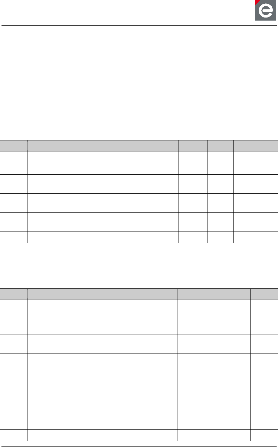
Table 8-1: Absolute maximum ratings
Symbol
Parameter
Condition
Min
Typ
Max
Unit
TOP
Operating temperature
-40
+85
°C
Tstorage
Storage temperature
-40
+125
°C
VPIN
Pin voltage with respect
to GND and VCC
GND
-0.3
VCC
+0.3
V
VCC
Maximum VCC pin
voltage
0
3.8
V
VESD
ESD robustness
Human Body Model
Charged Device Model
4
550
kV
V
PRF
Input RF level
+10
dBm
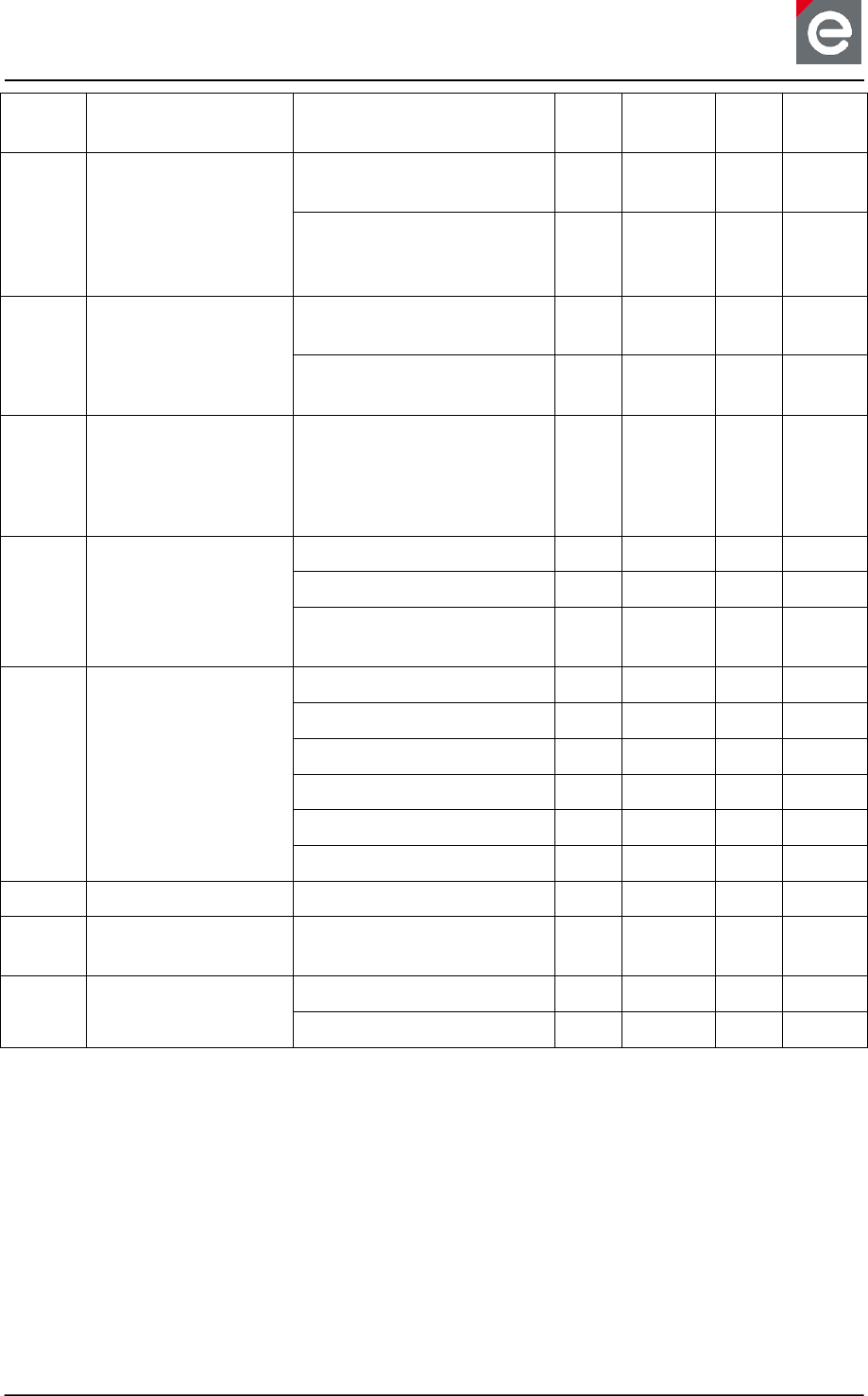
6.2. Electrical Characteristics
The data in the following table is measured at a temperature of 25°C with supply voltage of
3.3 V if not otherwise noted.
Table 8-2: Electrical specification data
Symbol
Parameter
Condition
Min
Typ
Max
Unit
VCC
Power supply
voltage
Default Mode for full
operation of data flash
2.5
3.3
3.6
V
For USB interface
3.0
3.3
3.6
V
IDDOTAU
Current consumption
OTAU
transceiver in RXON state
and data flash write
TBD
mA
IDD1
Current consumption
of parts
(data flash in
standby mode)
MCU running while(1) loop
3.4
mA
Transceiver in RXON state
11.8
mA
Transceiver in TXON state
13.8
mA
IDD2
Current consumption
MCU and data flash in
deep power down
5
22
µA
IDD3
Current consumption
(data flash only)
Read
4
12
mA
Page Program
10
20
PRF
RF transmit power
conducted
4
dBm
datasheet
Version 0.9
2017-09-13
deRFsamR21E-23S00/-23S20 datasheet
www.dresden-elektronik.de
Page 14 of 36
PRange
Output power range
16 steps configurable
transceiver output power
-17
4
dB
Pemit
RF transmit power
radiated deRFsamR21E-
23S00 (chip antenna)2
4
dBm
EIRP
radiated deRFsamR21E-
23S20 using antenna
Wimo 17013 (+5 dBi)
9
dBm
EIRP
Dlos
Maximum line of
sight range3
deRFsamR21E-23S00
(chip antenna)
200
m
deRFsamR21E-23S20
(2 dBi Gain antenna)
220
m
RXsens
Receiver sensitivity
Data Rate 250 kBit/s
Data Rate 500 kBit/s
Data Rate 1 MBit/s
Data Rate 2 MBit/s
-99
-94
-92
-86
dBm
dBm
dBm
dBm
PSPUR_TX
Transmitter spurious
emissions according
to EN 300328 V2.1.1
(as measured in
certification tests)
30 MHz to 1 GHz
-62
dBm
1 GHz to 4 GHz
-38
dBm
4 GHz to 12.75 GHz
-58
dBm
ESPUR_TX
Transmitter spurious
emissions according
to FCC 15.247
(as measured in
certification tests)
30 MHz to 200 MHz
35
dBµV/m
200 MHz to 1 GHz
22
dBµV/m
1 GHz to 4 GHz
36
dBµV/m
4 GHz to 26.5 GHz
48
dBµV/m
2.3 GHz to 2.4 GHz
53
dBµV/m
2.484 GHz to 2.5 GHz
61
dBµV/m
fCPU
Maximum MCU clock
48
MHz
fTRXosc
Transceiver oscillator
frequency
16
MHz
fTRXoscdev
Transceiver oscillator
frequency deviation
At 25°C
-10
+10
ppm
-40°C < TOP < +85°C
-20
+20
ppm
Note:
1. For FCC band edge compliance with deRFsamR21E-23S20 it is required to operate
Ch26 with not more than TX_PWR=0x7 (0 dBm).
2. Based on RF pattern measurement with USB powered Baseboard
3. Measured at height of 1.5 m above flat land of grass with transmit power 4 dBm.
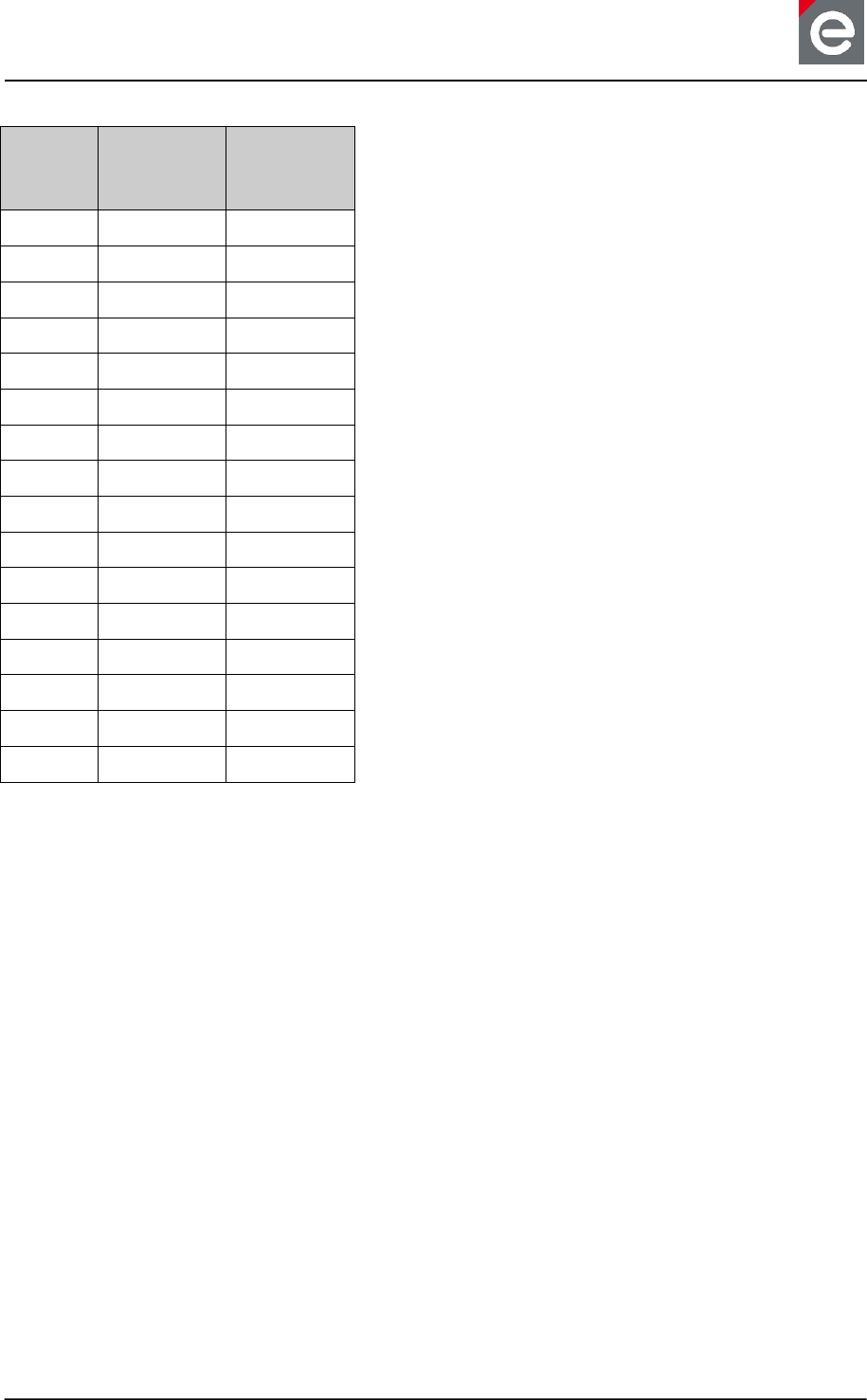
6.3. TX Power register settings
The output power of the transceiver can be configured with the TX_PWR register according
to Table 8-3.
datasheet
Version 0.9
2017-09-13
deRFsamR21E-23S00/-23S20 datasheet
www.dresden-elektronik.de
Page 15 of 36
Table 8-3: TX_PWR Register settings at 3.0V
TX_PWR
Value
TX Output
Power
[dBm]
Current
Consuption
[mA]1
0x0
4
13.8
0x1
3.7
0x2
3.4
0x3
3
0x4
2.5
0x5
2
0x6
1
0x7
0
11.8
0x8
-1
0x9
-2
0xA
-3
0xB
-4
0xC
-6
0xD
-8
0xE
-12
0xF
-17
7.2
Note:
1. Current consumption for transceiver only, MCU and data flash currents have to be
considered as well
6.4. Fuse setting
Fuses are used to configure the ATSAMR21E18 operation modes and clocks. This is mainly
done by internal commands which can be found in [1].
datasheet
Version 0.9
2017-09-13
deRFsamR21E-23S00/-23S20 datasheet
www.dresden-elektronik.de
Page 16 of 36
7. Onboard SPI Serial Flash
The module incorporates a 4 MBit data flash connected to the module by SPI bus. The data
flash connects to PA16-PA19 according to Table 9-1.
Table 9-1: Dataflash to microcontroller connection
Port
Function
Flash pin
Controller settings
PA16
MISO
SO
PA16 SERCOM1 or 3 PAD[0] DIPO=0x0
PA17
SCK
SCK
PA17 SERCOM1 or 3 PAD[1] DOPO=0x2
PA18
GPIO
SS
PA18 to be set low in software before SPI access
PA19
MOSI
SI
PA19 SERCOM1 or 3 PAD[3] DOPO=0x2
The signals in this table are available at module pins 7-10 as well. The module contains the
serial data flash AT25SF041 according to Table 9-2. Since the memory market is very
difficult at the moment, the module incorporates some alternative flash devices listed in
Table 9-3. This is done to avoid supply bottlenecks. To avoid problems, no specific flash ID
shall be used in the customer firmware. This section outlines basic usage instructions. For a
more detailed description refer to the datasheets of the flash devices.
Table 9-2: default serial data flash
Partnumber
Manufacturer
JEDEC ID (9Fh)
Datasheet reference
AT25SF041
Adesto
1F-84-01
[9]
Table 9-3: second source serial data flash list
Partnumber
Manufacturer
JEDEC ID (9Fh)
Datasheet reference
MX25V4006E
Macronix
C2-20-13
[10]
W25X40CL
Winbond
EF-30-13
[11]
W25Q40CL
Winbond
EF-40-13
[12]
7.1. Commands
To ease the implementation of the different flash devices Table 9-4 lists the commands and
their respective opcodes common to all the flash devices listed above.
Table 9-4: command table common to all flash options
Command
Opcode
Byte 2
Byte 3
Byte 4
Byte 5
Byte 6
Byte n
Write enable
06h
Write disable
04h
Read Status Register
05h
(S7-S0)
Write Status Register
01h
S7-S0
see*
Page Program
02h
A23-A16
A15-A8
A7-A0
(D7-D0)
(next
byte)
Up to 256
bytes
Sector Erase (4kB)
20h
A23-A16
A15-A8
A7-A0
Block Erase (64kB)
D8h
A23-A16
A15-A8
A7-A0
Chip Erase
C7h/60h
Power-down
B9h
Resume from Deep
Power Down
ABh
Resume from Deep
Power Down and
read ID
ABh
dummy
dummy
dummy
(IRD7-
IRD0)
datasheet
Version 0.9
2017-09-13
deRFsamR21E-23S00/-23S20 datasheet
www.dresden-elektronik.de
Page 17 of 36
Read Data (up to
30 MHz)
03h
A23-A16
A15-A8
A7-A0
(D7-D0)
(next
byte)
continuous
Fast Read (up to
70 MHz)
0Bh
A23-A16
A15-A8
A7-A0
dummy
(D7-D0)
continuous
Read Manufacturer
and Device ID
9Fh
(M7-M0)
(ID15-
ID8)
(ID7-ID0)
Read ID
90h
dummy
dummy
00h
(M7-M0)
(IRD7-
IRD0)
*make sure not to send a second byte since it may lead to locked and not resettable
protection with some of the flash devices
7.2. Status register
The status register is described in Table 9-5.
Table 9-5: flash status register
Bit
content
explanation
Type
S7
SRP
Software Protected
R/W
S6
0
Do not use (always set to 0)
R/W
S5
0
Do not use (always set to 0)
R/W
S4
BP2
Block Protection Bit 2
R/W
S3
BP1
Block Protection Bit 1
R/W
S2
BP0
Block Protection Bit 0
R/W
S1
WEL
Write Enable Latch status
R
S0
BUSY
Indicates ready/busy status
R
Status register bit S5 and S6 always have to be programmed to 0 to ensure proper operation
of the block protection according to Table 9-6. While reading ignore S5 and S6.
Table 9-6: block protection
BP2
BP1
BP0
Address Range
Portion
0
0
0
None
None
0
0
1
070000h-07FFFFh
Upper 1/8
0
1
0
060000h-07FFFFh
Upper 1/4
0
1
1
040000h-07FFFFh
Upper 1/2
1
X
X
000000h-07FFFFh
All
7.3. Flash Timings
Table 9-7 contains typical and maximum values for timings. Typical values refer to the
standard flash AT25SF041 while maximum values apply to all the listed flash devices.
Table 9-7: timings of onboard flash
Parameter
Typ
Max
Unit
Page Program
0.7
2.5
ms
Byte Program
5
us
Block erase 4K
60
300
ms
Block erase 64K
500
2200
ms
Chip Erase
4
10
s
tCSS
7
ns
tV Output Valid
time
8
ns
datasheet
Version 0.9
2017-09-13
deRFsamR21E-23S00/-23S20 datasheet
www.dresden-elektronik.de
Page 18 of 36
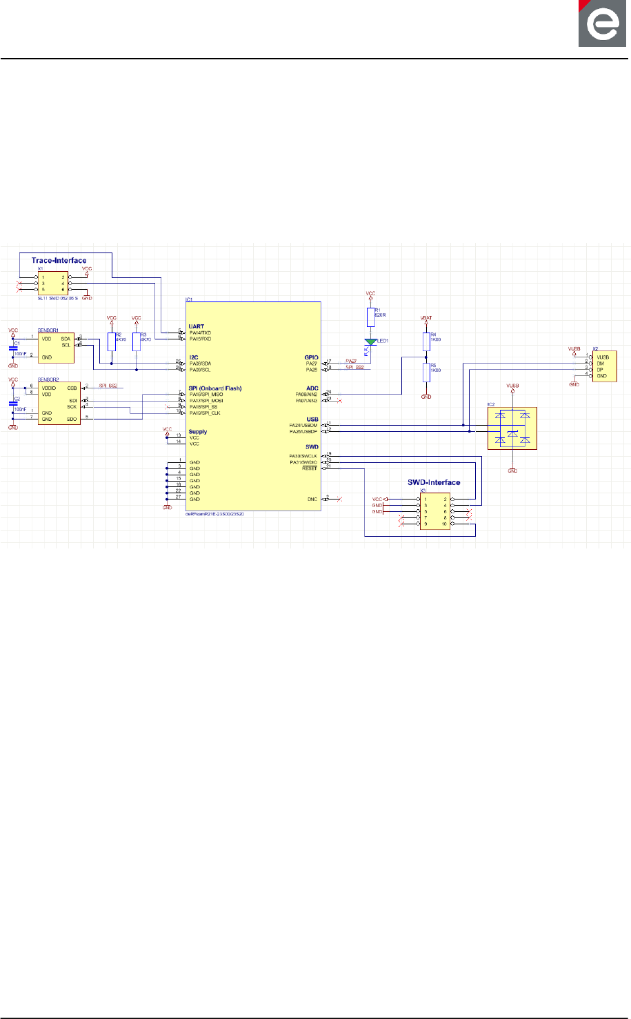
8. Recommended configuration
This chapter describes a recommended configuration which enables use of all frequently
used interfaces. The schematic symbol used in this chapter as well as a footprint can be
found in dresden elektronik Altium and Eagle libraries (see Section 7.3). Figure 10-1 shows
the schematic of a sample application. The sample application provides USB and
incorporates two sensors, a LED, an analogue input measuring the battery voltage and using
the UART interface through a 6-pin header for tracing. This configuration with all common
interfaces is shown in Figure 10-1.
Figure 10-1 configuration with all common interfaces
datasheet
Version 0.9
2017-09-13
deRFsamR21E-23S00/-23S20 datasheet
www.dresden-elektronik.de
Page 19 of 36
8.1. Signal description
The features of the controller can be mapped to different ports. How to configure the device
for the example configuration is described in this chapter. The serial interface functions are
organized in SERCOM units (Serial Communication Interface). These units consist of
4 Signals and can be mapped to several ports of the microcontroller. The configuration is
shown in Table 10-1.
Table 10-1: Pin configuration
Pin
Pad
Function
Config
05
PA14
UART/TXD
SERCOM2/PAD2
06
PA15
UART/RXD
SERCOM2/PAD3
07
PA16
SPI_MISO
SERCOM1/PAD0
08
PA17
SPI_MOSI
SERCOM1/PAD1
09
PA18
SPI_SS
Digital out
10
PA19
SPI_CLK
SERCOM1/PAD3
11
PA24
USBDM
12
PA25
USBDP
17
PA27
GPIO
Digital out
18
PA28
SPI_SS2
Digital out
19
PA30
SWD/SWCLK
20
PA31
SWD/SWDIO
21
-
RESET
23
PA07
ADC/AIN7
24
PA06
ADC/AIN6
25
PA08
I2C/SDA
SERCOM0/PAD0
26
PA09
I2C/SCL
SERCOM0/PAD1
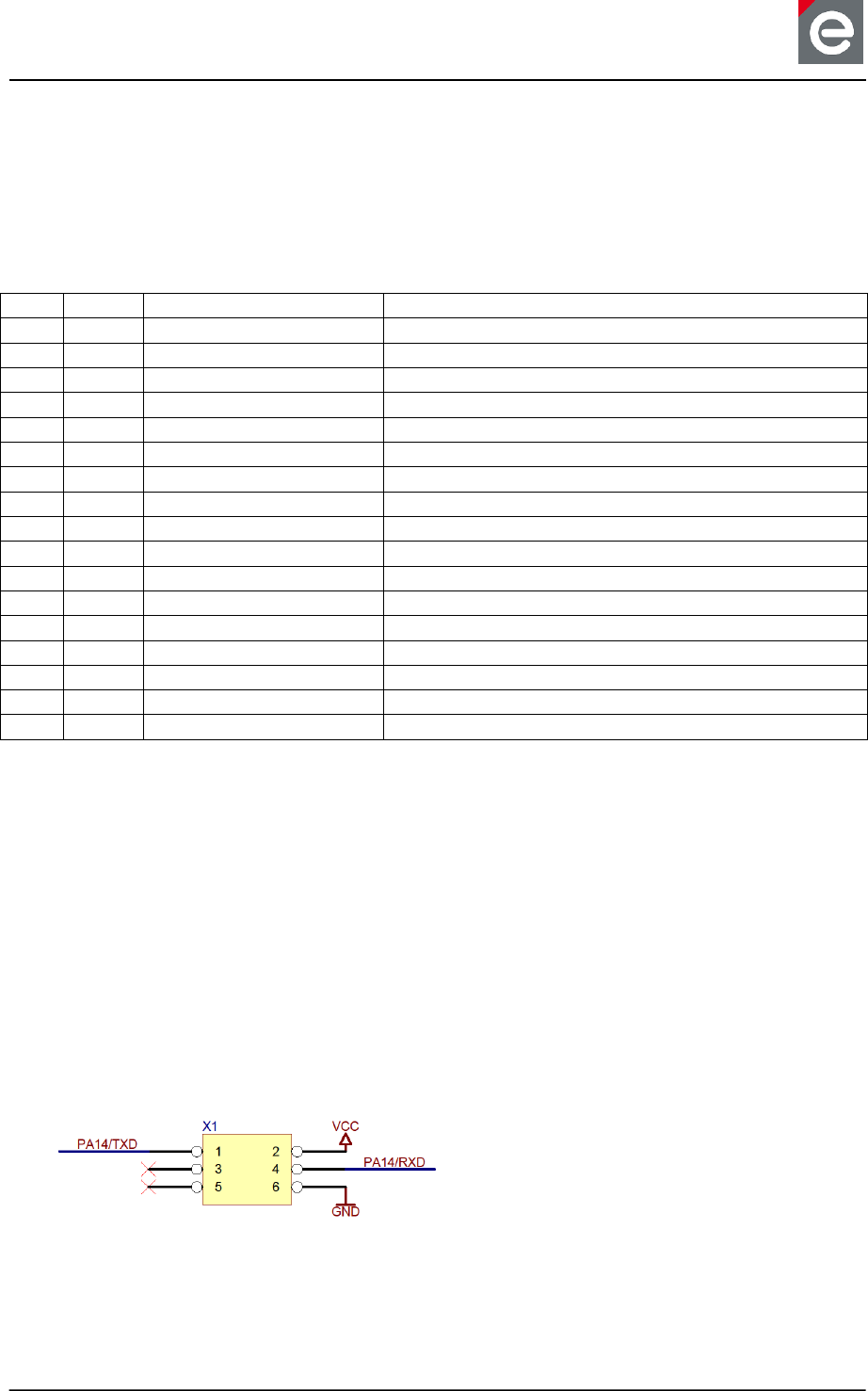
8.2. UART
The UART interface is a commonly used bidirectional interface for communication between
microcontrollers. The transmit (TXD) and receive (RXD) lines have to be connected directly
to the second device. TXD for the host controller is RXD for the client, the other signal works
accordingly.
For communication to a host with a different supply voltage domain it is necessary to use a
level-shifter part. We recommend the USB level shifter by dresden elektronik. The level-
shifter can be connected to the custom base board via 100 mil 2 x 3 pin header. The pin
assignment should be designed as below in Figure 10-2. For a UART connection it is
sufficient to use only TXD, RXD and GROUND signals.
1. PA14/TXD
2. VCC
3. Not connected
4. PA15/RXD
5. Not connected
6. GND
Figure 10-2: 100 mil / 2,54 mm 2 x 3 pin header for UART
datasheet
Version 0.9
2017-09-13
deRFsamR21E-23S00/-23S20 datasheet
www.dresden-elektronik.de
Page 20 of 36
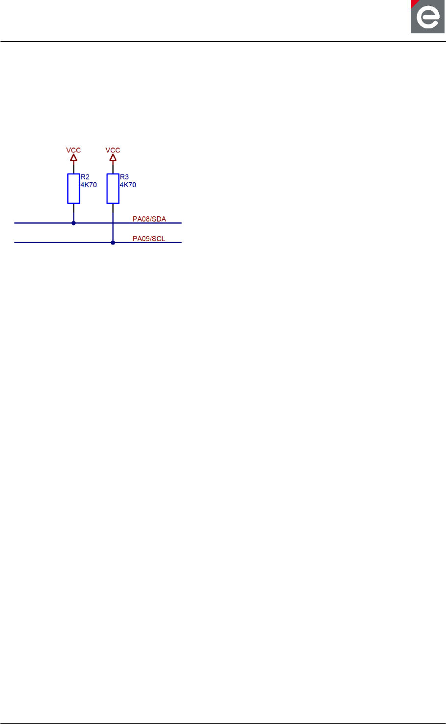
8.3. I2C (TWI)
The I2C (Inter-Integrated Circuit, also referred to as TWI – two wire interface) is a common
interface for sensor connection and it is able to connect several devices at one bus. There is
one clock signal (SCL) and a data signal (SDA). It is necessary to place pull-up resistors for
both lines externally to the radio module for proper function. We recommend the use of
4.7 kΩ resistors as shown in Figure 10-3.
Figure 10-3: Two Wire Interface
8.4. USB
The USB (Universal Serial Bus) interface complies with USB 2.1 specification. It supports
both device and embedded host modes. PA24 (USBDM) and PA25 (USBDP) are routed as
differential lines from the MCU to the radio module side contacts to pins 11 and 12. The
module power supply cannot be operated directly from a 5 V USB source. The module base
board has to implement the required voltage regulator for recommended voltage supply of
3.3 V. For USB operation a minimum supply voltage of 3.0 V is required.
8.5. SPI
The SPI (Serial Peripheral Interface) is a synchronous serial communication interface
commonly used in embedded systems. The SPI Interface on this module is used by the
onboard serial data flash. To add another device to the SPI Bus SCLK, MISO and MOSI can
be used, only another chip select signal (SS) is needed for each device. Any GPIO can be
used for this purpose, except pin 9 (PA18) since it is connected to the chip select of the
onboard data flash. In this example pin 18 (PA28) is used for the SPI Sensor chip select.
8.6. ADC
The module contains an ADC (Analog to Digital Converter) with 12-bit resolution. It supports
sample rates up to 350 ksps. Pin 23 and 24 (PA07 and PA06) are used in this configuration.
The internal reference voltage can be set to 1.0 V, VCC/1.48 and VCC/2.
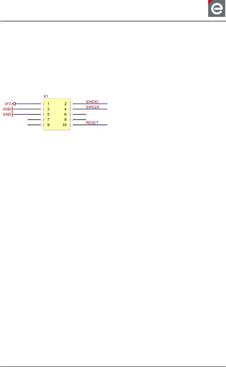
8.7. SWD
The SWD interface consists of clock signal (SWCLK) and data signal (SWDIO) as well as the
RESET signal for programming and debugging the microcontroller. More details on
programming can be found in Section 12.
8.8. GPIO
In this example pin 17 (PA27) and pin 18 (PA28) are reserved for GPIO usage, but nearly
every pin can be used as GPIO if not used otherwise.
8.9. Reset
The reset pin is low active and has an internal 10k pull-up resistor to power supply VCC.
datasheet
Version 0.9
2017-09-13
deRFsamR21E-23S00/-23S20 datasheet
www.dresden-elektronik.de
Page 21 of 36
9. Application Information
The PCB design of a radio module base board is important for a proper performance of
peripherals and the radio. The next subsections give design hints to create a custom base
board.
9.1. PCB Technology
The module is designed for use with standard PCB technology to reduce the costs and cover
a wide application range.
9.2. Power supply
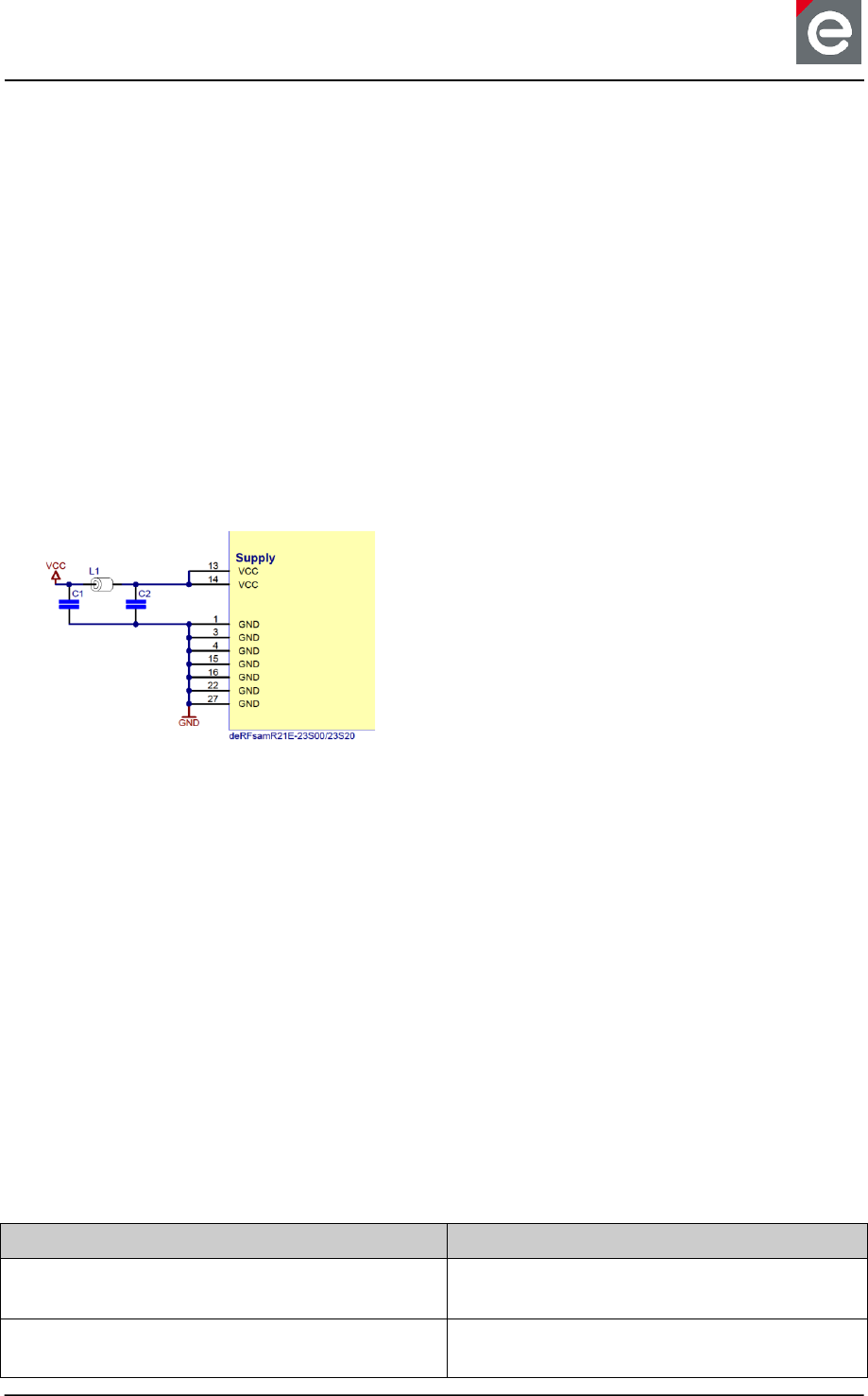
Power supply pins 13 and 14 have to be connected to a power domain of 2.5 to 3.6 V. No
external decoupling components are needed. For noisy environments it is recommended to
include a filter consisting of a ferrite or inductor and capacitors to reduce noise on the power
domain to the module. An example is shown in Figure 11-1. Place all components in near
proximity to each other and C2 between Pin 14 and 15 next to the module.
Figure 11-1: Power supply decoupling for noisy environments
9.3. Ground plane
The performance of RF applications mainly depends on the ground plane design. The often
used chip ceramic antennas are very tiny, but they need a proper ground plane to establish a
good radiation pattern. Every board design is different and cannot easily be compared to
each other. Some practical notes for the ground plane design are described below:
Regard to the design guideline of the antenna manufacturer
Use closed ground planes on the PCB edges on top and bottom layer
Connect the ground planes with lots of vias. Place it inside the PCB like a chessboard
and on the edges very closely.
9.4. Layers
The use of 2 or 4 layer PCB boards have advantages and disadvantages for the design of a
custom base board.
Table 11-1: 2 and 4 layer board properties in comparison
2 Layer board
4 Layer board
(-) only 2 layers available for routing traces and
design a proper ground area
(+) 4 layers available for routing traces and
design a proper ground area
(-) only 1 layer available for routing traces
below the module
(+) 3 layers available for routing traces
below the module
datasheet
Version 0.9
2017-09-13
deRFsamR21E-23S00/-23S20 datasheet
www.dresden-elektronik.de
Page 22 of 36
(-) no separate VCC plane usable
(+) separate VCC plane usable
(+) cheaper than 4 layers
(-) more expensive than 2 layers
9.5. Traces below the module
Signal traces should not be placed directly below the module to avoid short circuits:
Traces on top layer are not allowed under the module (see Figure 11-2)
Traces on mid layers and bottom layers are allowed (see Figure 11-2)
Figure 11-2: Layer design of 2 and 4 layer boards
9.6. Placement on the PCB
The PCB design of the radio module base board and placement affects the radio pattern. For
the deRFsamR21E-23S20 with coaxial u.FL connector usage, module placement is not
critical, since the radiating part is placed external to the module and can therefore be placed
everywhere on the board. If the RF-Pad is used, the placement shall be chosen for proper
RF design.
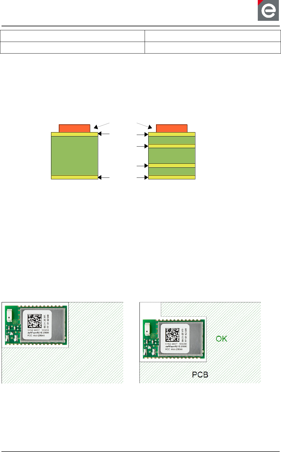
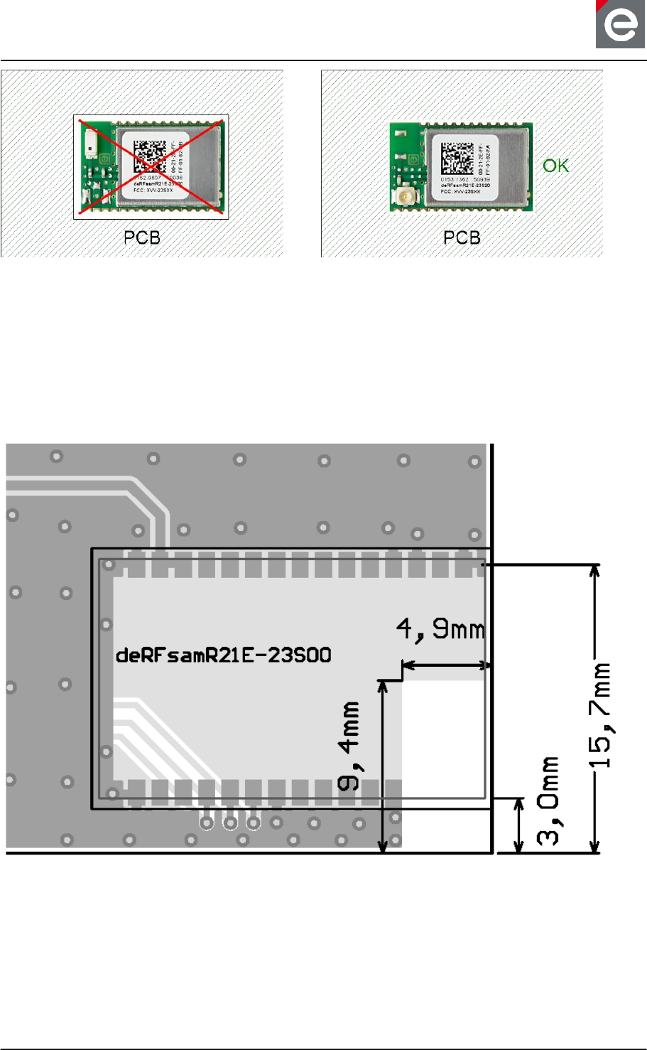
For deRFsamR21E-23S00 with integrated antenna the performance is strongly influenced by
the base board design. The module shall be placed at the edge of the base board. The chip
antenna has to be placed next to the edge as shown in the figures below. The antenna
design is optimized for use on 1.5 mm FR4 PCB baseboard. Best performance is obtained
with the module placed at the corner of the PCB with as much ground plane on the board as
possible.
Figure 11-3: Placing at the edge
Figure 11-4: Placing at the centre edge
Do not place the chip antenna radio module within the base board. This will cause a very
poor radio performance.
Top
Bottom
Mid 1
Mid 2
2 Layer 4 Layer
Module
4 Layer Traces under
module:
Not allowed
allowed
allowed
allowed
Traces under
module:
Not allowed
allowed
datasheet
Version 0.9
2017-09-13
deRFsamR21E-23S00/-23S20 datasheet
www.dresden-elektronik.de
Page 23 of 36
Figure 11-5: Placing in the centre with
antenna
Figure 11-6: Placing in the centre with RF pad
Do not place ground areas below the radio module and near the chip antenna (see Section
11.5 and 11.7).
9.7. Recommended layout for deRFsamR21E-23S00
For best performance of the deRFsamR21E-23S00 with chip antenna it is recommended to
place the module at a corner of the PCB according to Figure 11-7.
Figure 11-7 recommended layout for deRFsamR21E-23S00 module
The module antenna design of deRFsamR21E-23S00 is optimized for mounting on a
standard technology PCB with the following properties:
Two-layer board
Board material FR4
datasheet
Version 0.9
2017-09-13
deRFsamR21E-23S00/-23S20 datasheet
www.dresden-elektronik.de
Page 24 of 36
Board thickness of 1.55 mm
Copper layer thickness of 35 µm
Top and bottom solder
9.8. RF Design for deRFsamR21E-23S20
For deRFsamR21E-23S20 two options for the RF signal are available: using the coaxial u.FL
connector to connect an external antenna or if needed in the application, custom designed
RF circuitry using the RF-out pad.
Note: Please get in contact with dresden elektronik to advise for a custom FCC certified
design. If necessary dresden elektronik can provide RF part design data. This may
require signing a Non-Disclosure Agreement.
When designing RF traces on the base board a line impedance of 50 Ω shall be used.
Depending on the base board layer stack construction a microstrip or grounded coplanar
microstrip design can be implemented.
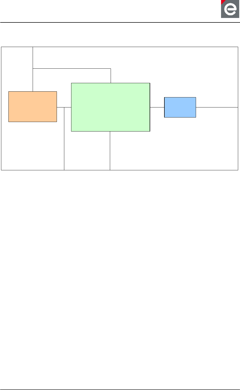
9.8.1. External front end and antenna diversity
The radio module deRFsamR21E-23S20 can be used with an external front end, including
power amplifier (PA) for transmission and low noise amplifier (LNA) for receiving, and
antenna diversity. Figure 11-8 shows a possible design as block diagram. A custom design
can contain a single PA or single LNA or a complete integrated front-end chip. It depends
mainly on the application. Furthermore, it is possible to include a RF switch for driving the
antenna diversity feature. An example block diagram is shown in Figure 11-8.
Figure 11-8: block diagram for external PA/LNA and antenna diversity control
The DIG1 to DIG4 signals of the transceiver are connected internally to the microcontroller
and have to be muxed on ports PA08, PA09, PA14 and PA15. DIG1 to DIG4 can be
activated as alternate pin output functions FECTRL[0..5] by the microcontroller. Please refer
to chapter 33 of ATSAMR21 datasheet [1].
Unbalanced RF output
The radio module deRFsamR21E-23S20 has a 50 Ω unbalanced RF output. For designs
with external RF power amplifier a RF switch is required to separate the TX and RX path.

datasheet
Version 0.9
2017-09-13
deRFsamR21E-23S00/-23S20 datasheet
www.dresden-elektronik.de
Page 25 of 36
RF switches to PA, LNA and antenna
The switch must have 50 Ω inputs and outputs for the RF signal. The switch control can be
realized with the DIG3 and DIG4 signal of the radio transceiver.
Power amplifier (PA)
The PA has to be placed on the TX path after the RF switch. It is important to regard the
PA’s manufacturer datasheet and application notes, especially for designing the power
supply and ground areas. A poor design could cause a very poor RF performance. For
energy efficiency it is useful to activate the PA only during TX signal transmission. In this
case the DIG3 signal can be used as switch for (de-)activating the PA. Some PAs have the
possibility to set them into sleep state. This application can be realized via a dedicated GPIO
pin.
Band-pass filter (BPF)
The use of a band-pass filter is optional. It depends on the PA properties. Some PAs have an
internal BPF and other do not have. The BPF is necessary to suppress spurious emissions of
the harmonics and to be compliant with national EMI limits. It is possible to use an integrated
BPF part or discrete parts. The advantage of the first variant is that the BPF characteristic is
known and published in the manufacturer’s datasheet.
Low noise amplifier (LNA)
The LNA can be used to amplify the received signal. Please refer to the manufacturer’s
datasheet for a proper design. The control can be done by DIG4 signal.
RF switch for antenna diversity
The switch must have 50 Ω inputs and outputs for the RF signal. It is possible to use a
separate switch with 2 inputs and 2 outputs or use another (third) switch following the switch
required for the PA/LNA. Antenna diversity switching can be controlled via DIG1.
Certification
The customer has to ensure, that custom front-end and antenna diversity designs based on
the radio module deRFsamR21E-23S20 meet all national regulatory requirements of the
assignment location and to have all necessary certifications, device registration or
identification numbers.
datasheet
Version 0.9
2017-09-13
deRFsamR21E-23S00/-23S20 datasheet
www.dresden-elektronik.de
Page 26 of 36
10. Programming
The update process of the radio module, the required software and hardware for
programming via SWD interface and the driver installation on different operating systems are
described in this chapter. Currently, the SWD interface is supported by several Atmel and
third party programmers and debuggers like Atmel ICE and Segger J-Link. Other
programmers that support ATSAMR21E18A will work as well.
For the programming the standard SWD header is recommended as 10pin 1.27 mm header
as shown in Figure 12-1.
Figure 12-1: Programming header
10.1. Software/Applications
For software development several options are available depending on your needs:
For low-cost embedded wireless applications the MiWi Stack from Microchip supports
the ATSAMR21. More information can be found at http://www.microchip.com/design-
centers/wireless-connectivity/embedded-wireless/802-15-4/software/miwi-protocol
For ZigBee 3.0 home automation projects Microchip offers the ZigBee 3.0 BitCloud
software stack. This stack is platform certified by the ZigBee Alliance. For more
information see
http://www.microchip.com/design-centers/wireless-connectivity/embedded-
wireless/802-15-4/zigbee-3-0
Please contact your local Microchip Sales Representative to get access to the
BitCloud Software Development Kit.
In Atmel Studio the Atmel Software Framework (ASF) offers a big number of
examples for ATSAMR21G18A. It is the same controller in a package with more
GPIO Pins available for the user. Some minor adjustments are necessary to allow the
examples to run on ATSAMR21E18A on this module.
Suitable compilers are GCC (v4.5.2) or IAR Compiler(IAR C/C++ Compiler for ARM v7.80.1)
for example.
Dresden elektronik offers software development services for with comprehensive experience
in ZigBee 3.0 and IEEE 802.15.4 wireless applications.
10.2. Clocks
The controller runs on 8 MHz RC-oscillator by default. Since the internal clock generation is
not very accurate, it is recommended to use the external transceiver oscillator to avoid
problems during communication for example by UART. To change the clock source to the
precise transceiver oscillator (±10 ppm at 25°C) the transceiver has to be configured for
clock output (CLKM) and the clock source at the controller has to be set to „GLCKIN“/“
GCLK_IO[1]“.
During deep sleep operation the clock source is best set to „OSCULP32K“ for minimized
current consumption. Further information can be found in [1].

datasheet
Version 0.9
2017-09-13
deRFsamR21E-23S00/-23S20 datasheet
www.dresden-elektronik.de
Page 27 of 36
10.3. Pre-flashed firmware
The radio modules will be delivered without pre-flashed firmware. Dresden elektronik
provides development services for industrial or ZigBee 3.0 compatible projects and the
modules can be delivered with custom firmware pre-programmed.

datasheet
Version 0.9
2017-09-13
deRFsamR21E-23S00/-23S20 datasheet
www.dresden-elektronik.de
Page 28 of 36
11. Radio certification
The modules deRFsamR21E-23S00 and deRFsamR21E-23S20 have received regulatory
approvals for modular devices in the United States and European countries. The modules
were also successfully tested according to IC regulations and are compliant but not certified
for Canada.
11.1. United States (FCC)
The deRFsamR21E-23S00 with onboard chip antenna and deRFsamR21E-23S20 with
coaxial u.FL connector comply with the requirements of FCC part 15.
To fulfil FCC Certification requirements, an OEM manufacturer must comply with the
following regulations:
The modular transmitter must be labelled with its own FCC ID number, and, if the FCC ID is
not visible when the module is installed inside another device, then the outside of the device
into which the module is installed must also display a label referring to the enclosed module.
This exterior label can use wording such as the following. Any similar wording that expresses
the same meaning may be used.
Sample label for radio module deRFsamR21E-23S00 and deRFsamR21E -23S20:
Contains FCC-ID: XVV-23SXX
This device complies with Part 15 of the FCC Rules. Operation is subject to the following two
conditions: (1) this device may not cause harmful interference, and (2) this device must
accept any interference received, including interference that may cause undesired operation.
The Original Equipment Manufacturer (OEM) must ensure that the OEM modular transmitter
must be labelled with its own FCC ID number. This includes a clearly visible label on the
outside of the final product enclosure that displays the contents shown below. If the FCC ID
is not visible when the equipment is installed inside another device, then the outside of the
device into which the equipment is installed must also display a label referring to the
enclosed equipment.
This equipment complies with Part 15 of the FCC Rules. Operation is subject to the following
two conditions: (1) this device may not cause harmful interference, and (2) this device must
accept any interference received, including interference that may cause undesired operation
(FCC 15.19).
Installers must be provided with antenna installation instructions and transmitter operating
conditions for satisfying RF exposure compliance. This device is approved as a mobile
device with respect to RF exposure compliance, and may only be marketed to OEM
installers.
Modifications not expressly approved by this company could void the user's authority to
operate this equipment (FCC section 15.21).
This equipment generates, uses, and can radiate radio frequency energy and, if not installed
and used in accordance with the instruction manual, may cause harmful interference to radio
communications.

datasheet
Version 0.9
2017-09-13
deRFsamR21E-23S00/-23S20 datasheet
www.dresden-elektronik.de
Page 29 of 36
11.2. European Union (ETSI)
Hereby, dresden elektronik ingenieurtechnik gmbh declares that the radio equipment types
deRFsamR21E-23S00 and deRFsamR21E-23S20 are in compliance with the Directive
2014/53/EU. The full text of the EU declaration of conformity is available at the following
internet address:
https://www.dresden-elektronik.de/funktechnik/solutions/wireless-light-control/eu-
conformity/?L=1.
If the deRFsamR21E-23S00 and deRFsamR21E-23S20 modules are incorporated into a
product, the manufacturer must ensure compliance of the final product to the European
harmonized EMC and low-voltage/safety standards. A Declaration of Conformity must be
issued for each of these standards and kept on file as described in Annex VI of the Radio
Equipment Directive 2014/53/EU.
The manufacturer must maintain a copy of the deRFsamR21E-23S00 and deRFsamR21E-
23S20 modules documentation and ensure the final product does not exceed the specified
power ratings, antenna specifications, and/or installation requirements as specified in the
user manual. If any of these specifications are exceeded in the final product, a submission
must be made to a notified body for compliance testing to all required standards.
The CE marking must be affixed to a visible location on the OEM product. The CE mark shall
consist of the initials "CE" taking the following form:
If the CE marking is reduced or enlarged, the proportions must be respected.
The CE marking must have a height of at least 5 mm except where this is not
possible on account of the nature of the apparatus.
The CE marking must be affixed visibly, legibly, and indelibly.
More detailed information about CE marking requirements can be found in [3].
datasheet
Version 0.9
2017-09-13
deRFsamR21E-23S00/-23S20 datasheet
www.dresden-elektronik.de
Page 30 of 36
11.3. Approved antennas
The deRFsamR21E-23S00 has an integrated chip antenna. The design is fully compliant
with all regulations.
The deRFsamR21E-23S20 is compliant with the listed approved antennas in Table 13-1.
Table 13-1: Approved antenna(s) and accessory
Approved antenna list
Type
Gain
Mount
Order code
Vendor / Supplier
External antenna
2400 to 2483.5 MHz
Rubber antenna
+5dBi (peak)
RP-
SMA
17013.RSMA
WiMo
U.FL-to-RP-SMA
pigtail, 15 cm
-0.5dB
BN-023769
dresden elektronik
Integrated antenna
2400 to 2483.5 MHz
Chip antenna
+0.5dBi (peak)
SMT
AMCA31-
2R450G-S1F-T
Abracon LLC
According to FCC KDB 178919 [5] it is allowed to substitute approved antennas through
equivalent antennas of the same type with equal or less antenna gain:
‘Equivalent antennas must be of the same type (e.g., yagi, dish, etc.), must be of
equal or less gain than an antenna previously authorized under the same FCC ID,
and must have similar in band and out-of-band characteristics (consult specification
sheet for cutoff frequencies).’
datasheet
Version 0.9
2017-09-13
deRFsamR21E-23S00/-23S20 datasheet
www.dresden-elektronik.de
Page 31 of 36
12. Ordering information
The product name includes the following information:
Table 14-1: Product name code
Product name code
Information
Code
Explanation
Product / Chipset
samR21E
ATSAMR21E18A
Frequency Range
2
2.4 GHz
Flash memory
3
256 kByte
Series
S
OEM module 2nd generation
Features
00
Onboard chip antenna
20
Coaxial u.FL connector and RF-OUT pad
Table 14-2: Ordering information
Ordering information
order number
Product name
Comments
BN-600097
deRFsamR21E-23S00
solderable radio module with onboard chip
antenna, no pre-flashed firmware
BN-600098
deRFsamR21E-23S20
solderable radio module with coaxial u.FL-
connector and RF-OUT pad, no pre-
flashed firmware
The modules will be delivered in Tape & Reel, for details see section 13.
deRF xxxx - x x x xx
Features
Form Factor
Flash Memory
Frequency Range
Product / Chipset
datasheet
Version 0.9
2017-09-13
deRFsamR21E-23S00/-23S20 datasheet
www.dresden-elektronik.de
Page 32 of 36
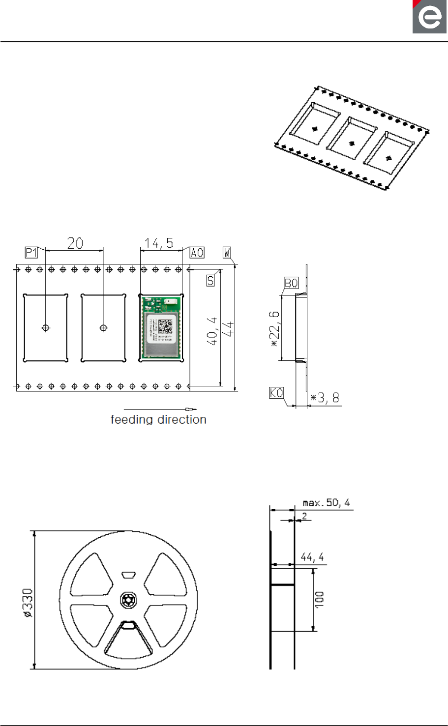
13. Packaging dimension
The modules will be delivered in Tape & Reel. The
reel quantity is 800 pcs, lower quantities will be
delivered in cut tape.
Tape dimensions
Reel dimensions
All dimensions are nominal and measured in mm.
datasheet
Version 0.9
2017-09-13
deRFsamR21E-23S00/-23S20 datasheet
www.dresden-elektronik.de
Page 33 of 36
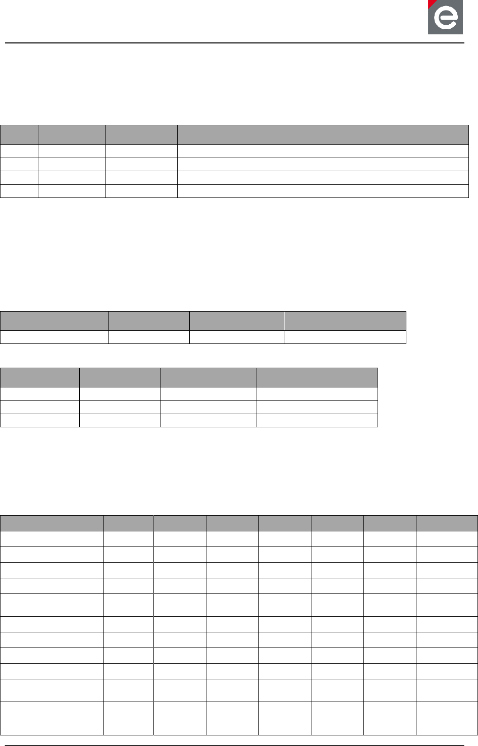
14. Soldering profile
Table 16-1 shows the recommended soldering profile for the radio modules.
Table 16-1: Soldering Profile
Profile Feature
Values
Average-Ramp-up Rate (217°C to Peak)
3°C/s max
Preheat Temperature 175°C ±25°C
180 s max
Temperature Maintained Above 217°C
60 s to 150 s
Time within 5°C of Actual Peak Temperature
20 s to 40 s
Peak Temperature Range
260°C
Ramp-down Rate
6°C/s max
Time 25°C to Peak Temperature
8 min max
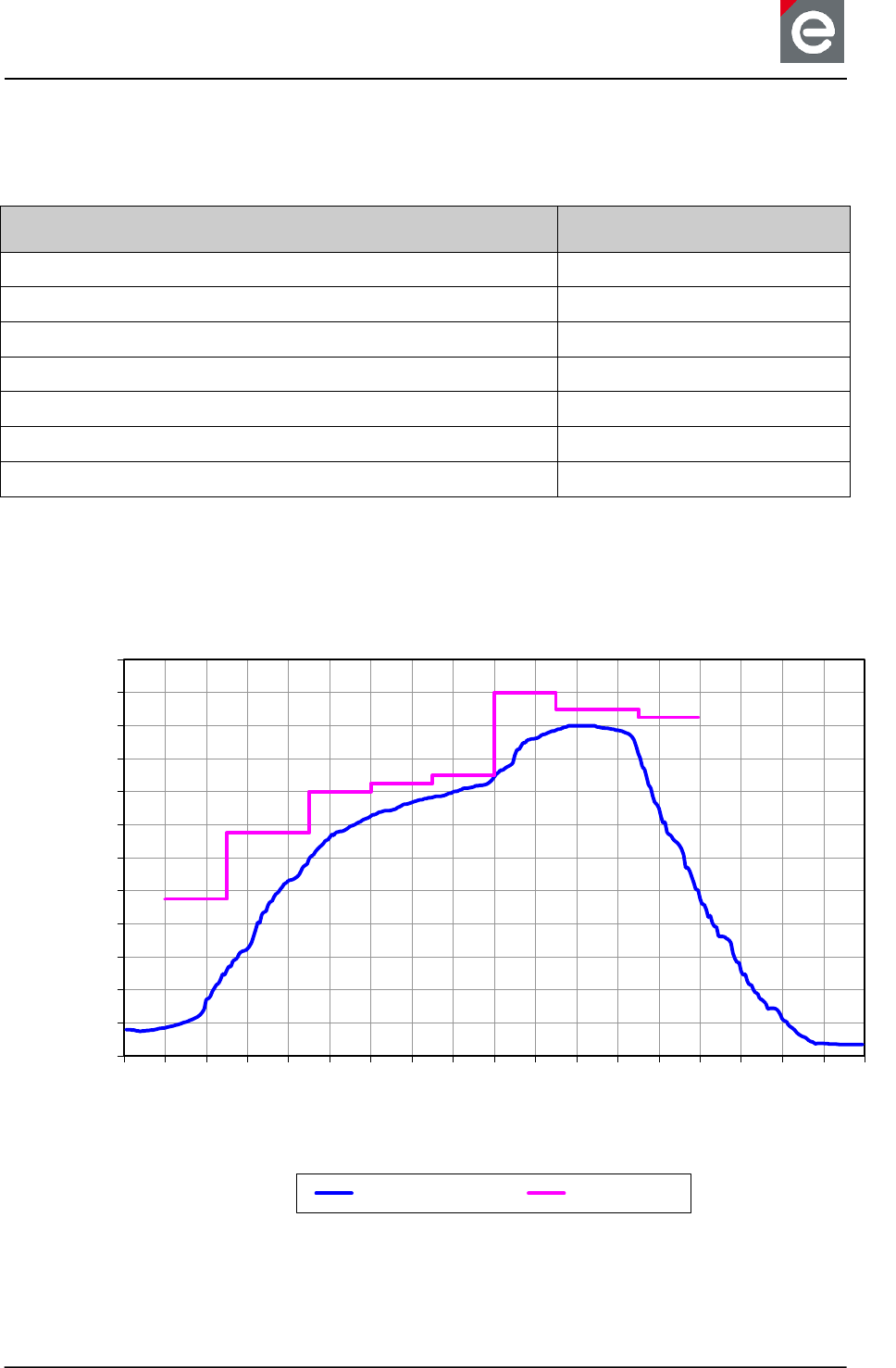
Figure 16-1 shows a recorded soldering profile for a radio module. The blue colored line
illustrates a temperature sensor placed next to the soldering contacts of the radio module.
The pink line shows the set temperatures depending on the zone within the reflow soldering
machine.
Figure 16-1: Recorded soldering profile
A solder process without supply of nitrogen causes a discoloration of the metal RF-shielding.
It is possible that the placed label shrinks due the reflow process.
40
60
80
100
120
140
160
180
200
220
240
260
280
0
20
40
60
80
100
120
140
160
180
200
220
240
260
280
300
320
340
360
T [°C]
t [s]
Measured Temp. Zone Temp.


datasheet
Version 0.9
2017-09-13
deRFsamR21E-23S00/-23S20 datasheet
www.dresden-elektronik.de
Page 35 of 36
16. References
[1] ATSAMR21E18A: Atmel SAM R21E / SAM R21G, SMART ARM-Based Wireless
Microcontroller; Datasheet, URL:
http://www.microchip.com/wwwproducts/en/ATSAMR21E18A
[2] AT86RF233: Low Power, 2.4GHz Transceiver for ZigBee, RF4CE, IEEE 802.15.4,
6LoWPAN, and ISM Applications; Datasheet, URL:
http://www.microchip.com/wwwproducts/en/at86rf233
[3] Directive 2014/53/EU, European Parliament and the Council, 16 April 2014, URL:
http://eur-lex.europa.eu/legal-content/en/ALL/?uri=CELEX:32014L0053
[4] Transmitter Module Equipment Authorization Guide; 996369 D01 Module Certification
Guide; FCC OET; URL:
https://apps.fcc.gov/oetcf/kdb/forms/FTSSearchResultPage.cfm?id=44637&switch=P
[5] Permissive Change Policy; 178919 D01 Permissive Change Policy; FCC OET; URL:
https://apps.fcc.gov/oetcf/kdb/forms/FTSSearchResultPage.cfm?id=33013&switch=P
[6] 2.4GHz Chip-Antenna AMCA31-2R450G-S1F-T by Abracon LLC; Datasheet; URL:
http://www.abracon.com/chip-antenna/AMCA31-2R450G-S1F-T.pdf
[7] 2.4GHz Rubber antenna 17013.xx by WiMo Antennen und Elektronik GmbH; Datasheet;
URL: http://www.wimo.com/download/17013.pdf
[8] Schematic and footprint library for Altium Designer®; URL: http://www.dresden-
elektronik.de/funktechnik/service/downloads/documentation/?eID=dam_frontend_push&d
ocID=2024
[9] Schematic and footprint library for EAGLE®; URL: http://www.dresden-
elektronik.de/funktechnik/service/downloads/documentation/?eID=dam_frontend_push&d
ocID=2023
[10] STEP model library for CAD tools; URL: http://www.dresden-
elektronik.de/funktechnik/service/downloads/documentation/?eID=dam_frontend_push&d
ocID=2022
[11] Link Config file Atmel Start
[12] Flash AT25SF041 by Adesto; Datasheet; URL: https://www.adestotech.com/wp-
content/uploads/DS-AT25SF041_044.pdf
[13] Flash MX25V4006E by Macronix; Datasheet; URL:
http://www.macronix.com/Lists/Datasheet/Attachments/6217/MX25V4006E,%202.5V,%2
04Mb,%20v1.9.pdf
[14] Flash W25X40CL by Winbond; Datasheet; URL: http://www.winbond.com/resource-
files/w25x40cl_f%2020140325.pdf
[15] Flash W25X40CL by Winbond; Datasheet; URL: http://www.winbond.com/resource-
files/da00-w25q40cle1.pdf

datasheet
Version 0.9
2017-09-13
deRFsamR21E-23S00/-23S20 datasheet
www.dresden-elektronik.de
Page 36 of 36
dresden elektronik ingenieurtechnik gmbh
Enno-Heidebroek-Straße 12
01237 Dresden
GERMANY
Phone +49 351 31850-0
Fax +49 351 31850-10
Email wireless@dresden-elektronik.de
Trademarks and acknowledgements
IEEE 802.15.4™ is a trademark of the Institute of Electrical and Electronics
Engineers (IEEE).
ZigBee® is a registered trademark of the ZigBee Alliance.
All trademarks are registered by their respective owners in certain countries only. Other
brands and their products are trademarks or registered trademarks of their respective
holders and should be noted as such.
Disclaimer
This note is provided as-is and is subject to change without notice. Except to the extent prohibited by
law, dresden elektronik ingenieurtechnik gmbh makes no express or implied warranty of any kind with
regard to this guide, and specifically disclaims the implied warranties and conditions of merchantability
and fitness for a particular purpose. dresden elektronik ingenieurtechnik gmbh shall not be liable for
any errors or incidental or consequential damage in connection with the furnishing, performance or
use of this guide.
No part of this publication may be reproduced, stored in a retrieval system, or transmitted in any form
or any means electronic or mechanical, including photocopying and recording, for any purpose other
than the purchaser’s personal use, without the written permission of dresden elektronik
ingenieurtechnik gmbh.
Copyright © 2017 dresden elektronik ingenieurtechnik gmbh. All rights reserved.